EP3783789A1 - Control method for controlling resonant power converter, and resonant power converter - Google Patents
Control method for controlling resonant power converter, and resonant power converter Download PDFInfo
- Publication number
- EP3783789A1 EP3783789A1 EP18915276.2A EP18915276A EP3783789A1 EP 3783789 A1 EP3783789 A1 EP 3783789A1 EP 18915276 A EP18915276 A EP 18915276A EP 3783789 A1 EP3783789 A1 EP 3783789A1
- Authority
- EP
- European Patent Office
- Prior art keywords
- switching element
- timing
- diode
- current
- controller
- Prior art date
- Legal status (The legal status is an assumption and is not a legal conclusion. Google has not performed a legal analysis and makes no representation as to the accuracy of the status listed.)
- Pending
Links
- 238000000034 method Methods 0.000 title claims abstract description 26
- 239000003990 capacitor Substances 0.000 claims abstract description 75
- 238000006243 chemical reaction Methods 0.000 claims abstract description 42
- 238000001514 detection method Methods 0.000 claims description 9
- 238000010586 diagram Methods 0.000 description 11
- 230000007423 decrease Effects 0.000 description 7
- 230000003071 parasitic effect Effects 0.000 description 6
- 230000000630 rising effect Effects 0.000 description 3
- 238000012546 transfer Methods 0.000 description 3
- 238000013459 approach Methods 0.000 description 2
- 230000003247 decreasing effect Effects 0.000 description 2
- 238000012986 modification Methods 0.000 description 2
- 230000004048 modification Effects 0.000 description 2
- 238000012544 monitoring process Methods 0.000 description 2
- 230000003111 delayed effect Effects 0.000 description 1
- 238000007599 discharging Methods 0.000 description 1
- 230000000694 effects Effects 0.000 description 1
- 238000010992 reflux Methods 0.000 description 1
- 230000007704 transition Effects 0.000 description 1
Images













Classifications
-
- H—ELECTRICITY
- H02—GENERATION; CONVERSION OR DISTRIBUTION OF ELECTRIC POWER
- H02M—APPARATUS FOR CONVERSION BETWEEN AC AND AC, BETWEEN AC AND DC, OR BETWEEN DC AND DC, AND FOR USE WITH MAINS OR SIMILAR POWER SUPPLY SYSTEMS; CONVERSION OF DC OR AC INPUT POWER INTO SURGE OUTPUT POWER; CONTROL OR REGULATION THEREOF
- H02M7/00—Conversion of AC power input into DC power output; Conversion of DC power input into AC power output
- H02M7/42—Conversion of DC power input into AC power output without possibility of reversal
- H02M7/44—Conversion of DC power input into AC power output without possibility of reversal by static converters
- H02M7/48—Conversion of DC power input into AC power output without possibility of reversal by static converters using discharge tubes with control electrode or semiconductor devices with control electrode
- H02M7/53—Conversion of DC power input into AC power output without possibility of reversal by static converters using discharge tubes with control electrode or semiconductor devices with control electrode using devices of a triode or transistor type requiring continuous application of a control signal
- H02M7/537—Conversion of DC power input into AC power output without possibility of reversal by static converters using discharge tubes with control electrode or semiconductor devices with control electrode using devices of a triode or transistor type requiring continuous application of a control signal using semiconductor devices only, e.g. single switched pulse inverters
- H02M7/539—Conversion of DC power input into AC power output without possibility of reversal by static converters using discharge tubes with control electrode or semiconductor devices with control electrode using devices of a triode or transistor type requiring continuous application of a control signal using semiconductor devices only, e.g. single switched pulse inverters with automatic control of output wave form or frequency
- H02M7/5395—Conversion of DC power input into AC power output without possibility of reversal by static converters using discharge tubes with control electrode or semiconductor devices with control electrode using devices of a triode or transistor type requiring continuous application of a control signal using semiconductor devices only, e.g. single switched pulse inverters with automatic control of output wave form or frequency by pulse-width modulation
-
- H—ELECTRICITY
- H02—GENERATION; CONVERSION OR DISTRIBUTION OF ELECTRIC POWER
- H02M—APPARATUS FOR CONVERSION BETWEEN AC AND AC, BETWEEN AC AND DC, OR BETWEEN DC AND DC, AND FOR USE WITH MAINS OR SIMILAR POWER SUPPLY SYSTEMS; CONVERSION OF DC OR AC INPUT POWER INTO SURGE OUTPUT POWER; CONTROL OR REGULATION THEREOF
- H02M7/00—Conversion of AC power input into DC power output; Conversion of DC power input into AC power output
- H02M7/42—Conversion of DC power input into AC power output without possibility of reversal
- H02M7/44—Conversion of DC power input into AC power output without possibility of reversal by static converters
- H02M7/48—Conversion of DC power input into AC power output without possibility of reversal by static converters using discharge tubes with control electrode or semiconductor devices with control electrode
-
- G—PHYSICS
- G01—MEASURING; TESTING
- G01R—MEASURING ELECTRIC VARIABLES; MEASURING MAGNETIC VARIABLES
- G01R19/00—Arrangements for measuring currents or voltages or for indicating presence or sign thereof
- G01R19/165—Indicating that current or voltage is either above or below a predetermined value or within or outside a predetermined range of values
- G01R19/16533—Indicating that current or voltage is either above or below a predetermined value or within or outside a predetermined range of values characterised by the application
- G01R19/16538—Indicating that current or voltage is either above or below a predetermined value or within or outside a predetermined range of values characterised by the application in AC or DC supplies
-
- H—ELECTRICITY
- H02—GENERATION; CONVERSION OR DISTRIBUTION OF ELECTRIC POWER
- H02M—APPARATUS FOR CONVERSION BETWEEN AC AND AC, BETWEEN AC AND DC, OR BETWEEN DC AND DC, AND FOR USE WITH MAINS OR SIMILAR POWER SUPPLY SYSTEMS; CONVERSION OF DC OR AC INPUT POWER INTO SURGE OUTPUT POWER; CONTROL OR REGULATION THEREOF
- H02M1/00—Details of apparatus for conversion
- H02M1/32—Means for protecting converters other than automatic disconnection
-
- H—ELECTRICITY
- H03—ELECTRONIC CIRCUITRY
- H03F—AMPLIFIERS
- H03F3/00—Amplifiers with only discharge tubes or only semiconductor devices as amplifying elements
- H03F3/20—Power amplifiers, e.g. Class B amplifiers, Class C amplifiers
- H03F3/21—Power amplifiers, e.g. Class B amplifiers, Class C amplifiers with semiconductor devices only
- H03F3/217—Class D power amplifiers; Switching amplifiers
- H03F3/2176—Class E amplifiers
-
- H—ELECTRICITY
- H02—GENERATION; CONVERSION OR DISTRIBUTION OF ELECTRIC POWER
- H02M—APPARATUS FOR CONVERSION BETWEEN AC AND AC, BETWEEN AC AND DC, OR BETWEEN DC AND DC, AND FOR USE WITH MAINS OR SIMILAR POWER SUPPLY SYSTEMS; CONVERSION OF DC OR AC INPUT POWER INTO SURGE OUTPUT POWER; CONTROL OR REGULATION THEREOF
- H02M1/00—Details of apparatus for conversion
- H02M1/0003—Details of control, feedback or regulation circuits
- H02M1/0009—Devices or circuits for detecting current in a converter
-
- H—ELECTRICITY
- H02—GENERATION; CONVERSION OR DISTRIBUTION OF ELECTRIC POWER
- H02M—APPARATUS FOR CONVERSION BETWEEN AC AND AC, BETWEEN AC AND DC, OR BETWEEN DC AND DC, AND FOR USE WITH MAINS OR SIMILAR POWER SUPPLY SYSTEMS; CONVERSION OF DC OR AC INPUT POWER INTO SURGE OUTPUT POWER; CONTROL OR REGULATION THEREOF
- H02M1/00—Details of apparatus for conversion
- H02M1/0048—Circuits or arrangements for reducing losses
- H02M1/0054—Transistor switching losses
- H02M1/0058—Transistor switching losses by employing soft switching techniques, i.e. commutation of transistors when applied voltage is zero or when current flow is zero
-
- H—ELECTRICITY
- H02—GENERATION; CONVERSION OR DISTRIBUTION OF ELECTRIC POWER
- H02M—APPARATUS FOR CONVERSION BETWEEN AC AND AC, BETWEEN AC AND DC, OR BETWEEN DC AND DC, AND FOR USE WITH MAINS OR SIMILAR POWER SUPPLY SYSTEMS; CONVERSION OF DC OR AC INPUT POWER INTO SURGE OUTPUT POWER; CONTROL OR REGULATION THEREOF
- H02M1/00—Details of apparatus for conversion
- H02M1/32—Means for protecting converters other than automatic disconnection
- H02M1/327—Means for protecting converters other than automatic disconnection against abnormal temperatures
-
- H—ELECTRICITY
- H02—GENERATION; CONVERSION OR DISTRIBUTION OF ELECTRIC POWER
- H02M—APPARATUS FOR CONVERSION BETWEEN AC AND AC, BETWEEN AC AND DC, OR BETWEEN DC AND DC, AND FOR USE WITH MAINS OR SIMILAR POWER SUPPLY SYSTEMS; CONVERSION OF DC OR AC INPUT POWER INTO SURGE OUTPUT POWER; CONTROL OR REGULATION THEREOF
- H02M7/00—Conversion of AC power input into DC power output; Conversion of DC power input into AC power output
- H02M7/42—Conversion of DC power input into AC power output without possibility of reversal
- H02M7/44—Conversion of DC power input into AC power output without possibility of reversal by static converters
- H02M7/48—Conversion of DC power input into AC power output without possibility of reversal by static converters using discharge tubes with control electrode or semiconductor devices with control electrode
- H02M7/4815—Resonant converters
-
- H—ELECTRICITY
- H02—GENERATION; CONVERSION OR DISTRIBUTION OF ELECTRIC POWER
- H02M—APPARATUS FOR CONVERSION BETWEEN AC AND AC, BETWEEN AC AND DC, OR BETWEEN DC AND DC, AND FOR USE WITH MAINS OR SIMILAR POWER SUPPLY SYSTEMS; CONVERSION OF DC OR AC INPUT POWER INTO SURGE OUTPUT POWER; CONTROL OR REGULATION THEREOF
- H02M7/00—Conversion of AC power input into DC power output; Conversion of DC power input into AC power output
- H02M7/42—Conversion of DC power input into AC power output without possibility of reversal
- H02M7/44—Conversion of DC power input into AC power output without possibility of reversal by static converters
- H02M7/48—Conversion of DC power input into AC power output without possibility of reversal by static converters using discharge tubes with control electrode or semiconductor devices with control electrode
- H02M7/4815—Resonant converters
- H02M7/4818—Resonant converters with means for adaptation of resonance frequency, e.g. by modification of capacitance or inductance of resonance circuits
-
- Y—GENERAL TAGGING OF NEW TECHNOLOGICAL DEVELOPMENTS; GENERAL TAGGING OF CROSS-SECTIONAL TECHNOLOGIES SPANNING OVER SEVERAL SECTIONS OF THE IPC; TECHNICAL SUBJECTS COVERED BY FORMER USPC CROSS-REFERENCE ART COLLECTIONS [XRACs] AND DIGESTS
- Y02—TECHNOLOGIES OR APPLICATIONS FOR MITIGATION OR ADAPTATION AGAINST CLIMATE CHANGE
- Y02B—CLIMATE CHANGE MITIGATION TECHNOLOGIES RELATED TO BUILDINGS, e.g. HOUSING, HOUSE APPLIANCES OR RELATED END-USER APPLICATIONS
- Y02B70/00—Technologies for an efficient end-user side electric power management and consumption
- Y02B70/10—Technologies improving the efficiency by using switched-mode power supplies [SMPS], i.e. efficient power electronics conversion e.g. power factor correction or reduction of losses in power supplies or efficient standby modes
Definitions
- the present invention relates to a resonance type power conversion device and a control method for controlling the resonance type power conversion device.
- a wireless power transfer device comprising and a monitoring circuit and an E-type amplifier circuit including a switching element.
- This wireless power transfer device switches the switching element to the open position during the first transfer and switched the switching element to the close position when determining that the value indicating the voltage of the switching element is below the threshold value, to perform zero volt switching.
- the switching element under a state of high-speed on, repeated off, by monitoring the voltage change of the switching element, the voltage of the switching element is less than the threshold since it must detect a limited time, it becomes difficult to continuously perform zero-volt switching, there is a problem that the switching loss is increased.
- An object to be solved by the present invention is to provide a control method and resonance type power conversion device for controlling resonance type power conversion device, which can suppress switching losses.
- the present invention detects a polarity of current flowing through parallel circuit connected in parallel to a first switching element by using a sensor included in a voltage resonance circuit; and controls an operating condition of a first switching element depending on the polarity of the current detected by the sensor to solve the above problem.
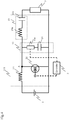
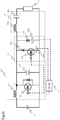
- Fig. 1 is a schematic diagram of the resonance type power conversion device.
- the resonance type power conversion device includes an input power supply 1, a load 2, a controller 3, and a voltage resonance circuit 10.
- Input power supply 1 is connected to the inputs of the voltage resonance circuit 10.
- the input power supply 1 is, for example, a constant-voltage source of direct current.
- the load 2 is connected to the output of the voltage resonance circuit 10.
- a pair of power supply lines is connected between input power supply 1 and load 2, the power supply line on the positive electrode side is connected between the positive electrode of the input power supply 1 and the load 2, and the power supply line on the negative electrode side is connected between the negative electrode of the input power supply 1 and the load 2.
- Load 2 is a motor, etc., and is connected to an output terminal of a voltage resonance circuit.
- the controller 3 converts the power input from input power supply 1 by controlling on and off of the switching element 12 included in voltage resonance circuit 10 and outputs the converted power to Load 2.
- the voltage resonance circuit 10 is E class inverter-circuit and has a choke coil 11, a switching element 12, a parallel circuit 13, a capacitor 14, and a resonance circuit 15.
- the choke coil 11 is connected to the positive electrode of the input power supply 1.
- the switching element 12 is a transistor (switching device) such as a MOSFET. Note that, in the following description, MOSFET is used as switching element 12.
- a higher potential side terminal (Drain Terminal) of the switching element 12 is connected to a connection point A, and a lower potential side terminal (Source Terminal) of the switching element 12 is connected to a power line on the negative side.
- the connection point A is pointed on the power line on the positive side and a point at which the choke coil 11 and switching element 12 are connected.
- the parallel circuit 13 is a circuit connected in parallel to the switching element 12, and is a connection circuit for connecting between the positive power supply line and the negative power supply line.
- the Sensor 13a is connected to the parallel circuit 13. The sensor 13a detects current flowing through the parallel circuit 13 and outputs the detected values to the controller 3.
- Capacitor 14 is connected in parallel to the switching element 12 and is connected between the power supply line on the positive side and the power supply line on the negative side.
- the choke coil 11 and the capacitor 14 form an amplifier circuit.
- the resonance circuit 15 is an LC resonance circuit connected resonant coil 15a and the resonant capacitor 15b in series.
- the resonance circuit 15 is connected between the switching element 12 and the load 2. Note that, resonance circuit 15 is not limited to an LC series circuit in which LCs are connected in series, as shown in Fig. 1 , but may be another resonance circuit.
- the controller 3 outputs a drive signal to the control terminal (gate terminal) of the switching element 12.
- the drive signal is a signal for switching the switching element 12 on and off.
- the drive signal is represented by a square wave.
- the controller 3 detects polarity of current flowing in parallel circuit 13 by the positive and negative values of the detected current detected by the sensor 13a.
- the controller 3 controls operating condition of the switching element 12 depending on the polarity of the power detected by sensor 13a.
- the operating condition of the switching element 12 specifies the switching timing when switching element 12 is switched on and off by predetermined period. In other words, changing operating condition of the switching element 12 changes a timing for turn on and/or turn-off of the switching element 12.
- the controller 3 controls operating condition of the switching element 12 by changing a duty cycle of the drive signals and/or the drive cycle.
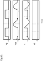
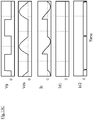
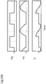
- Fig. 2 is a graph showing a waveform of the drive signal and a waveform of the voltage applied across switching element 12.
- Vg denotes the gate-voltage of the switching element 12.
- Vds denotes the voltage across the switching element 12 (drain-source voltage).
- the voltage across switching element 12 rises sinusoidally and then drops, resulting in a zero voltage across switching element 12. Then, when the voltage across switching element 12 is zero, if the drive signal rises, the zero-volt switching (hereinafter, also referred to as ZVS) is satisfied.
- ZVS zero-volt switching
- the graph shown in Fig. 2 (a) shows the voltage waveform when satisfied ZVS
- the graph shown in Fig. 2 (b) shows the voltage waveform when ZVS is not satisfied.
- the drive signal rises and switching element 12 is turned on while the voltage across switching element 12 is zero. Therefore, the voltage across switching element 12 changes to zero during the on-period after the voltage across switching element 12 reaches zero.
- the voltage across switching element 12 is a waveform as shown in Fig. 2(b) .
- the voltage across switching element 12 is a waveform as shown in Fig. 2(c) .
- the capacitance value of the resonant capacitor 15b is reduced from the capacitance value of the resonant capacitor 15b when the ZVS is satisfied, the voltage across switching element 12 is shifted in a waveform as shown in Fig. 2 (b) .
- Detected values of sensor 13a are decided by the voltage across switching element 12 and the impedance of parallel circuit 13 including sensor 13a. Therefore, controller 3, from the detected value of sensor 13a, or both end voltages of the switching element 12 is a state shown in Fig. 2 (b) , both end voltages of the switching element 12 determines whether the state shown in Fig. 2 (c) . Then, controller 3 controls operating condition of the switching element 12 so that the voltage across switching element 12 becomes the waveform shown in Fig. 2 (a) .
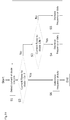
- Fig. 3 is a flowchart showing control flows of the controller 3.
- the controller 3 by outputting the drive signal of a predetermined period to the control terminal of the switching element 12, cyclically switches the on-off of the switching element 12. Apart from such switching operation control, the controller 3 executes the following control flows. Note that controller 3 repeatedly executes the control flows shown in Fig. 3 in accordance with timing for turning on the switching element 12.
- step S1 the controller 3 detects current flowing to parallel circuit 13 at timing for turn on the switching element 12 by sensor 13a.
- the controller 3 detects polarity of current detected by sensor 13a, and determines whether or not current of positive direction flows through the parallel circuit 13.
- the controller 3 executes the control flow in step S4.
- Positive direction is the direction in which current flows from the power supply line on the positive side to the power supply line on the negative side.
- Step S3 When current of positive direction does not flows through the parallel circuit 13, in Step S3, the controller 3 detects polarity of current detected by sensor 13a and determines whether current of negative direction flows through the parallel circuit 13. When current of negative direction flows through the parallel circuit 13, the controller 3 executes the control flow in step S6.
- step S4 When current of positive direction flows through the parallel circuit 13, since the voltage across switching element 12 is in the state of Fig. 2 (b) , in step S4, the controller 3 increases the frequency of the drive signal than the present frequency. Then, the controller 3 executes the control process of step S1.
- step S5 controller 3 decreases the frequency of the drive signal lower than the present frequency. Then, the controller 3 executes the control process of step S1.
- Step S6 the controller 3 sets the current frequency to the frequency of the driving signal.
- the frequency for satisfying the ZVS is decided. That is, the controller 3, by repeatedly executing the control loop from step S1 to step S5, in timing for turning on the switching element 12, so that current does not flow through the parallel circuit 13, operating condition of the switching element 12 is controlled.
- the sensor 13a is used to detect polarity of current flowing through the parallel circuit 13, and operating condition of the switching element 12 is controlled depending on polarity of the detected current.
- timing for turning on the switching element 12 deviates from timing when ZVS is satisfied.
- operating condition of the switching element 12 is controlled. This reduces the voltage applied to switching element 12 when the switching element 12 is turned on. As a result, the switching loss can be reduced.
- the controller 3, in the control flow of step S4, increases the duty ratio of the driving signal than the current duty ratio. Further, controller 3, in the control flow of step S5, the duty ratio of the driving signals may be lowered than the current duty ratio. Then, the controller 3, in the control flow of step S6, may sets the current duty ratio to the duty ratio of the driving signal.
- controller 3 the control flow of the control flow in step S4 and S5, may be adjusted both the frequency and the duty ratio of the drive signals.
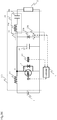
- sensor 13a may be connected in series with respect to capacitor 14.
- the connecting circuits of the sensor 13a and the capacitor 14 correspond to the parallel circuit 13.
- the controller 3 detects polarity of current of capacitor 14 using sensor 13a, and controls operating condition of the switching element 12 depending on the detection result.
- the control of operating condition of the switching element 12 is similar to the control flow shown in Fig. 3 .
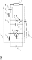
- Fig. 5 is a block diagram of a resonance type power conversion device according to another embodiment of the present invention.
- the difference is that a diode 13b is provided.
- Other features are the same as those in the above-described first embodiment and the description thereof is incorporated herein.
- a parallel circuit 13 has a sensor 13a and a diode 13b.
- a parallel circuit 13 is connected between lower potential side and the connection point A of the switching element 12.
- Conductive direction of the diode 13b is the direction in which the forward direction current flows from lower potential side of the switching element 12 toward the connection point A. That is, the anode of the diode 13b is connected to the power supply line on the negative electrode side, the cathode of the diode 13b is connected to the power supply line on the positive electrode side.
- the sensor 13s detects current (hereinafter also referred to as diode current) flowing to diode 13b.
- the controller 3 outputs a drive signal of a predetermined period to the control terminal of the switching element 12, and switches turn on and turn-off of the switching element 12.
- the controller 3 determines whether or not the forward direction current flows to the diode 13a from the detected values detected by the sensor 13a.
- the controller 3 controls operating condition of the switching element 12 depending on the determination result.
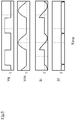
- Fig. 6A Fig and 6B the driving signal (Vg) of the switching element 12, the voltage (Vds) across the switching element 12, current (Ic) flowing to the capacitor 14, and current (Id) flowing to the diode 13b is explained below.
- Fig. 2 is a graph showing the characteristics of Vg, Vds, Ic, and Id.
- Ic, Id positive and negative current
- the form of the voltage (Vds) and current (Ic, Id) is like waveform as shown in Fig. 6A .
- the capacitance value of the resonant capacitor 15b when increased than the capacitance value of the resonant capacitor 15b at the time ZVS is satisfied, the form of the voltage (Vds) and current (Ic, Id) is like a waveform as shown in Fig. 6B .
- Fig. 7 is a flowchart showing control flows of the controller 3.
- the controller 3 by outputting a drive signal of a predetermined period to the control terminal of the switching element 12, cyclically switches the on-off of the switching element 12. Apart from such switching operation control, the controller 3 executes the following control flows. Note that, the controller 3, when starting the control of the resonance-side power converter, when the operating state of the load 2 fluctuates, or, at any timing during operation of the resonance-type power resonance device, executes the control flow shown in Fig.7 .
- step S1 the controller 3 detects current flowing through the parallel circuit 13 by the sensor 13a.
- step S2 the controller 3 determines whether or not current is flowing through the diode 13b. When the diode current is flowing, the voltage across switching element 12 is in a state as shown in Fig. 6B .
- step S3 the controller 3 lowers the frequency of the drive signal below the frequency before the change so that timing for turning on the switching element 12 is slower than timing before the change. When the diode current does not flow, the voltage across switching element 12 is in a state as shown in the Fig. 6A .
- step S4 the controller 3 increases the frequency of the drive signal above the frequency before the change so that timing for turn on of the switching element 12 is faster than timing before the change.
- step S5 the controller 3 sets the frequency after the change to the frequency of the drive signal.
- the ZVS area represents the region in which the drive frequency ZVS is satisfied.
- the frequency of the driving signal becomes higher than the frequency before one period while the forward direction current is not flowing through the diode 13b, as shown by the arrow P in Fig. 8 , the frequency of the driving signal approaches the frequency when ZVS is satisfied. Further, when the frequency of the driving signal becomes lower than the frequency before one cycle while the forward direction current is flowing through diode 13b, as shown by the arrow Q in Fig. 8 , the frequency of the driving signal approaches the frequency when ZVS is satisfied. Thus, it is possible to reduce the voltage applied to switching element 12 when switching element 12 is turned on.
- polarity of the diode current flowing to the diode 13b is detected in a state in which switching element 12 is turned on at timing of predetermined period, timing for turning on switching element 12 is made slower than timing of predetermined period when forward direction current flows to the diode 13b, and timing for turn on switching element 12 is made faster than timing of predetermined period when diode current does not flows.
- the frequency of the driving signal in order to set the frequency of the driving signal close to the frequency at the time of satisfying ZVS, it can be identified whether the frequency should be increased or decreased by using the result of whether the diode 13b is energized or not energized.
- the controller 3, in the control flow of step S3, may lower the duty ratio of the driving signal below the current duty ratio. Further, the controller 3, in the control flow of step S4, may increase the duty ratio of the drive signal than the current duty ratio.
- the controller 3 in the control flows the steps S3 and S4, may adjust both the frequency and the duty ratio of the drive signals.
- the forward voltage of the diode 13b when switching element 12 has a parasitic diode, the forward voltage of the diode 13b may be smaller than the forward voltage of the parasitic diode. Thus, it is possible to flow a lot of current to diode 13b in order to more stably detect diode current.
- the forward voltage of the diode 13b may be larger than the forward voltage of the parasitic diode. Thus, since current flowing to the diode 13b is suppressed, it is possible to reduce current tolerance of the diode 13b, and it is possible to suppress the costs of the diode 13b.
- Fig. 9 is a graph showing the characteristics of the voltage (Vg, Vds) and current (Ic, Id) when ZVS is satisfied.
- Vg denotes the gate voltage of the switching element 12
- Vds denotes the voltage across the switching element 12
- Ic denotes current flowing to the capacitor 14, and Id denotes current flowing to the diode 13b.
- Fig. 10 is a flowchart showing the control flows of the controller 3.
- the controller 3 by outputting a drive signal of a predetermined period to the control terminal of the switching element 12, cyclically switches the on-off of the switching element 12. Apart from such switching operation control, the controller 3 executes the following control flows. Note that, the controller 3, when starting the control of the resonance-side power converter, when the operating state of the load 2 fluctuates, or, at any timing during operation of the resonance-type power resonance device, executes the control flow shown in Fig. 10 .
- step S1 the controller 3 detects current flowing through the parallel circuit 13 by sensor 13a.
- step S2 the controller 3 determines whether or not current flows to diode 13b.
- Step S3 the controller 3 determines whether or not the previous diode current has flowed by using the previous detected value of sensor 13a. The determination in step S3 may use the determination result in step S2 when the control flow shown in Fig. 12 was previously executed. Then, when the previous diode current was flowing, in step S4, the controller 3 lowers the frequency of the drive signal below the previous frequency so that the timing for turning on the switching element 12 is slower than the previous timing.
- step S5 when it is determined that current does not flow through the diode 13b, in step S5, the controller 3 increases the frequency of the drive signal to be higher than the frequency before the change, and timing to turn on switching element 12 is made faster than timing before the change. That is, by repeating the control loop of step from S1 to S5, the frequency of the drive signal is gradually changed.
- step S6 the controller 3 sets the current frequency to the frequency of the driving signal.
- the frequency for satisfying the ZVS is decided.
- the ZVS area represents the region of the driving frequency at which ZVS is satisfied.
- S indicates the frequency at the time of control start
- E indicates the frequency at the time of control end, i.e. the frequency set in the control flow of step S6.
- the frequency of the drive signal is gradually increased from a state lower than the frequency at the time of satisfying ZVS, and the frequency of the drive signal is brought close to the frequency at the time of satisfying ZVS (corresponding to the arrow P in Fig. 11 ).
- a gradual increase in the frequency of the drive signals results in a gradual increase in timing for turn on of the switching element 12.
- the controller 3 gradually increases the frequency of the drive signal, ZVS is satisfied when shifting from a state in which the diode 13b is not energized to a state in which the diode 13b is energized. Therefore, the controller 3 gradually increases the frequency of the drive signal, by detecting that forward direction current starts flowing by using the detected value of sensor 13 a, it is possible to set the frequency when ZVS is satisfied.
- the frequency of the drive signal is gradually lowered from a state higher than the frequency at the time of satisfying ZVS, and the frequency of the drive signal is brought close to the frequency at the time of satisfying ZVS (corresponding to the arrow Q in Fig. 11 ).
- a gradual decrease in the frequency of the drive signals results in a gradual decrease in timing for turning on the switching element 12.
- the frequency of the driving signal is lower than the frequency region when ZVS is satisfied, when it is further lowered, the state shifts from the state in which the diode 13b is energized to a state in which the diode 13b is not energized. Then, in the control flow shown in Fig.
- the frequency increases. Then, when the frequency of the driving signal is increased, the state shifts from the state in which the diode 13b is not energized to a state in which the diode 13b is energized, and ZVS is satisfied. Therefore, the controller 3 gradually lowers the frequency of the drive signal to detect that a state of the diode 13b is from the state in which the diode 13b is energized to a state in which the diode 13b is not energized. After that, the controller 3 can set the frequency when ZVS is satisfied by increasing the frequency of the drive signal and detecting that the forward direction current starts flowing by using the detected value of the sensor 13a.
- the timing for turning on the switching element 12 when a state changes from a first state(the diode 13b energized state) in which the forward direction current does not flow to diode 13b to a second state (the diode 13b non-energized state) in which the forward direction current flows to diode 13b, , the timing for turning on the switching element 12 is set to the timing changed by second state.
- ZVS can be continuously performed, it is possible to suppress the switching loss.
- controller 3 in the control flow of step S5, the duty ratio of the driving signal may be increased from the current duty ratio. Further, the controller 3, in the control flow of step S4, the duty ratio of the driving signals may be lowered than the current duty ratio.
- the controller 3 in the control flow of the control flow of the steps S4 and S5, the frequency and the duty ratio of the drive signals may be adjusted.
- Fig. 12 is a block diagram of a resonance type power conversion device according to another embodiment of the present invention.
- the circuit configuration of the parallel circuit 13 is different.
- Other configurations are the same as the second embodiment described above, and the description of the first to third embodiments is appropriately incorporated.
- the parallel circuit 13 has a sensor 13, a diode 13b, a switching element 13c, a sensor 13d, and a diode 13e.
- the parallel circuit 13 is connected between lower potential side of the switching element 12 and the connection point A.
- the conductive direction of the diode 13b and 13e is the direction in which the forward direction current flows from the lower potential side of the switching element 13 to the connection point A. That is, the anode of the diode 13b is connected to the power supply line on the negative electrode side via the switching element 13c, and the cathode of the diode 13b is connected to the power supply line on the positive electrode side.
- the anode of the diode 13e is connected to the power supply line on the negative electrode side
- the cathode of the diode 13e is connected to the power supply line on the positive electrode side.
- the sensor 13a detects current flowing to diode 13b
- the sensor 13d detects current flowing to diode 13e.
- the switching element 13c is connected in series with the diode 13b.
- the diode 13e is connected in parallel to the series circuit of the diode 13b and the switching element 13c.
- the controller 3 controls on/off of the switching element 13c using a drive signal similar to the drive signal of the switching element 12. That is, the switching element 12 and the switching element 13c switch on and off synchronously.
- the controller 3 determines whether or not the forward direction current flows through diode 13a from the detected values of the sensor 13a.
- the controller 3 determines whether or not the forward direction current flows through the diode 13e from the detected values of the sensor 13d.
- the controller 3 controls operating condition of the switching element 12 depending on these determined results.
- the forward voltage of the diode 13b is lower than the forward voltage of the diode 13e. Further, when the switching element 13c is turned on, so that the current flows through the diode 13b and the current does not flow to the diode 13e, the circuit elements included in the voltage converting circuit is selected.
- FIGs. 13A-13C are graphs showing the characteristics of Vg, Vds, Ic, Id1, and Id2.
- Fig. 13A and 13B show the voltages and current waveforms when ZVS is not satisfied.
- Fig. 13C shows the voltages and current waveforms when ZVS is true.
- the voltage (Vds) and current (Ic, Id1, Id2) is a waveform as shown in Fig. 13A .
- the voltage (Vds) and current (Ic, Id1, Id2) is a waveform as shown in Fig. 13B .
- the current flows to the diode 13e when ZVS is satisfied, but the current does not flow to diode 13e when ZVS is not satisfied, as shown in Figs. 13A and 13B .
- the current flowing through the diode 13e when ZVS is satisfied flows before the switching element 13c is turned on, the forward direction current flows through the diode 13e without flowing to diode 13b.
- the forward direction current flows to diode 13b and does not flow to diode 13e.
- the forward voltage of the diode 13b is smaller than the forward voltage of the diode 13e, when ZVS is not satisfied, the forward direction current flows to diode 13b, not to diode 13e.
- controller 3 by detecting whether or not the forward direction current flows through diode 13b, 13e, it can be determined whether the waveforms of the voltages (Vds) and current (Ic, Id1, Ids) are any of the states in Figs. 13A to 13C .
- Fig. 14 is a flowchart showing the control flow of the controller 3.
- the controller 3 by outputting a drive signal of a predetermined period to the control terminal of the switching element 12, cyclically switches turn on-off of the switching element 12. Apart from such switching operation control, the controller 3 executes the following control flows. Note that, the controller 3, when starting the control of the resonance-side power converter, when the operating state of the load 2 fluctuates, or at any timing during operation of the resonance-type power resonance device, executes the control flows shown in Fig. 14 .
- step S1 the controller 3 detects the current flowing in parallel circuit 13 by sensor 13a and 13d.
- step S2 the controller 3 determines whether the current flows in diode 13e.
- the controller 3 executes the control in step S6.
- step S3 the controller 3 determines whether or not the current flows to diode 13b.
- step S4 the controller 3 lowers the frequency of the drive signal below the frequency before the change so that the timing for turning on the switching element 12 is slower than the timing before the change. Then, the process returns to step S1.
- step S5 the controller 3 increases the frequency of the drive signal to be higher than the frequency before the change and makes the timing for turning on the switching element 12 faster than the timing before the change. Then, the process returns to step S1. In step S6, the controller 3 sets the present frequency to the frequency of the drive signal. Thus, the frequency for satisfying the ZVS is decided.
- the ZVS area represents the region of the driving frequency at which ZVS is satisfied.
- S indicates the frequency at the time of control start
- E indicates the frequency at the time of control end, i.e. the frequency set in the control flow of step S6.
- the frequency of the drive signal is gradually increased from a state lower than the frequency at the time of satisfying ZVS, and the frequency of the drive signal is set close to the frequency at the time of satisfying ZVS (corresponding to the arrow P in Fig. 15 ).
- a gradual increase in the frequency of the drive signals results in a gradual increase in the timing for turning on the switching element 12.
- the controller 3 gradually increases the frequency of the drive signal, shifting from a state in which the diode 13b is not energized to the diode 13b is energized is a state in which ZVS is satisfied. Therefore, the controller 3 gradually increases the frequency of the drive signal, by detecting that the forward direction current starts flowing by using the detected value of sensor 13d, the frequency when ZVS is satisfied can be set.
- the frequency of the drive signal is gradually lowered from a state higher than the frequency at the time of satisfying ZVS, and the frequency of the drive signal is brought close to the frequency at the time of satisfying ZVS (corresponding to the arrow Q in Fig. 15 ).
- a gradual decrease in the frequency of the drive signals results in a gradual decrease in the timing for turning on the switching element 12.
- the controller 3 gradually lowers the frequency of the drive signal, shifting from a state in which the diode 13b is not energized to the diode 13b is energized is a state in which ZVS is satisfied. Therefore, the controller 3 can set the frequency when ZVS is satisfied by gradually lowering the frequency of the drive signal and detecting that the forward direction current starts flowing from the detected value of the sensor 13d.
- polarity of current flowing to the diode 13e is detected while switching element 12 is turned on at timing of the predetermined period, when the forward direction current does not flow to the diode 13e, the timing for turning on the switching element 12 is changed from the timing of the predetermined period, and when the forward direction current flows to the diode 13e, timing for turning on the switching element 12 is not changed from the timing of predetermined period.
- ZVS can be continuously performed, it is possible to suppress the switching loss.
- the controller 3, in the control flow of step S5, the duty ratio of the driving signal may be increased and is higher than the current duty ratio. Further, the controller 3, in the control flow of step S4, the duty ratio of the driving signals may be lowered than the current duty ratio.
- the controller 3, in the control flows of steps S4 and S5, may adjust both the frequency and the duty ratio of the drive signals.
- Fig. 16 is a block diagram of a resonance type power conversion device according to another embodiment of the present invention.
- the difference is that a temperature sensor 16 is provided.
- Other configurations are the same as the second embodiment described above, and the descriptions of the first to fourth embodiments are appropriately incorporated.
- the temperature sensor 16 for detecting the temperature of the switching element 12 is provided.
- the temperature sensor 16 such as a thermistor is used.
- the temperature sensor 16 outputs the detected value to the controller 3.
- the controller 3 controls operating condition of the switching element 12 depending on the detected values of the sensor 13b and the temperature sensor 16 of sensor.
- the controller 3 can determine whether ZVS is satisfied based on detection temperature. When it is determined that ZVS is not satisfied, the controller 3 controls operating condition of the switching element 12 depending on polarity of the current flowing to diode 13b.
- Fig. 17 is a flowchart showing the control flows of the controller 3.
- the controller 3 by outputting a drive signal of a predetermined period to the control terminal of the switching element 12, cyclically switches the turn on-off of the switching element 12. Apart from such switching operation control, the controller 3 executes the following control flows. Note that, the controller 3, when starting the control of the resonance-side power converter, when the operating state of the load 2 fluctuates, or, at any timing during operation of the resonance-type power resonance device, executes the control flows shown in Fig. 17 .
- step S1 the controller 3 detects current flowing to diode 13a by the sensor 13b, and detects temperature of the switching element 12 by the temperature sensor 16.
- step S2 the controller 3 determines whether or not detection temperature is equal to or greater than a predetermined threshold. When the detection temperature is less than a predetermined threshold, the controller 3 performs the control of step S6.
- step S3 the controller 3 determines whether or not current flows to diode 13a.
- step S4 the controller 3 lowers the frequency of the drive signals below the frequency before the change so that the timing for turning on the switching element 12 is slower than timing before the change. Then, the process returns to step S1.
- step S5 the controller 3 increases the frequency of the drive signal above the frequency before the change and makes timing to turn on switching element 12 faster than timing before the change. Then, the process returns to step S1.
- step S6 The controller 3 sets the present frequency to the frequency of the drive signal. Thus, the frequency for satisfying the ZVS is decided.
- the controller 3, in the control flow of step S5, the duty ratio of the driving signal may be increased from the current duty ratio. Further, the controller 3, in the control flow of step S4, the duty ratio of the driving signals may be lowered than the current duty ratio.
- controller 3 the control flow of the control flow and step S5 in step S4, may be adjusted both the frequency and the duty ratio of the drive signals.
- Fig. 18 is a block diagram of a resonance type power conversion device according to another embodiment of the present invention.
- the difference is that a capacitor 14 is included in parallel circuit 13.
- Other configurations are the same as the first embodiment described above, and the description of the first to fifth embodiments are appropriately incorporated.
- parallel circuit 13 has a sensor 13a and a capacitor 14.
- the sensor 13a detects current flowing in capacitor 14.
- FIGs. 19A and 19B are graphs showing the characteristics of Vg, Vds, Ic.
- Figs. 19A and 19B show the voltages and current waveforms when ZVS is not satisfied.
- the voltage (Vds) and current (Ic) is a waveform as shown in Fig. 19A .
- the capacitance value of the resonant capacitor 15b is increased from the capacitance value of the resonant capacitor 15b when satisfied ZVS, the voltage (Vds) and current (Ic) is a waveform as shown in Fig. 19B .
- Fig. 20 is a flowchart illustrating a control flow of the controller 3.
- the controller 3 by outputting a drive signal of a predetermined period to the control terminal of the switching element 12, cyclically switches the on-off of the switching element 12. Apart from such switching operation control, the controller 3 executes the following control flows.
- the controller 3 when starting the control of the resonance-side power converter, when the operating state of the load 2 fluctuates, or, at any timing during operation of the resonance-type power resonance device, executes the control flow shown in Fig. 20 .
- step S1 the controller 3 detects current flowing to capacitor 14 by sensor 13a.
- step S2 the controller 3 determines whether or not current (capacitor current) of capacitor 14 flowing immediately before the switching element 12 is turned on in negative direction.
- capacitor current of negative direction since the voltage across switching element 12 is in the state shown in Fig. 19B , in step S3, the controller 3 makes the frequency of the drive signal lower than the frequency before the change and timing to turn on switching element 12 slower than timing before the change.
- step S4 increases the frequency of the drive signal above the frequency before the change and makes timing to turn on switching element 12 faster than timing before the change.
- step S5 the controller 3 sets the frequency after the change to the frequency of the drive signal.
- the controller 3, in the control flow of step S4, the duty ratio of the driving signal may be increased is higher than the current duty ratio. Further, the controller 3, in the control flow of step S3, may lower the duty ratio of the driving signals than the current duty ratio.
- the controller 3 in the control flows of the steps S3 and S4, may adjust both the frequency and the duty ratio of the drive signals.
- capacitor 14 is used as the capacitance component connected in parallel with the switching element 12, it is also possible to attach the element having a new capacitance component in addition to capacitor 14.
- Fig. 21 is a graph showing the characteristics of the voltage (Vg, Vds) and current (Ic, Id) when satisfied ZVS.
- Vg denotes the gate voltage of the switching element 12
- Vds denotes the voltage across the switching element 12
- Ic denotes current flowing to capacitor 14.
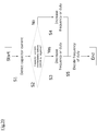
- Fig. 22 is a flowchart illustrating control flows of the controller 3.
- the controller 3 by outputting a drive signal of a predetermined period to the control terminal of the switching element 12, cyclically switches turn on-off of the switching element 12. Apart from such switching operation control, the controller 3 executes the following control flows. Note that, the controller 3, when starting the control of the resonance-side power converter, when the operating state of the load 2 fluctuates, or, at any timing during operation of the resonance-type power resonance device, executes the control flows shown in Fig. 22 .
- step S1 the controller 3 detects current flowing to capacitor 14 by sensor 13a.
- step S2 the controller 3 determines whether or not capacitor current is zero immediately before turning on the switching element 12. When the capacitor current is zero, the controller 3 performs the control in step S6.
- step S3 the controller 3 determines whether or not the capacitor current of negative direction flows.
- step S4 the controller 3 lowers the frequency of the drive signal below the frequency before the change so that timing for turning on the switching element 12 slows than timing before the change. Then, the process returns to step S1.
- step S5 when capacitor current of positive direction is flowing, in step S5, the controller 3 increases the frequency of the drive signal above the frequency before the change so that timing for turning on the switching element 12 is faster than timing before the change. Then, the process returns to step S1. In step S6, the controller 3 sets the present frequency to the frequency of the drive signal. Thus, the frequency for satisfying the ZVS is determined.
- the conductivity of capacitor 14 and the relationship between the frequencies of the drive signals is explained below.
- the ZVS area represents the region of the driving frequency at which ZVS is satisfied.
- S indicates the frequency at the time of control start
- E indicates the frequency at the time of control end, i.e. the frequency set in the control flow of step S6.
- the frequency of the drive signal is gradually increased from a state lower than the frequency at the time of satisfying ZVS, and the frequency of the drive signal is close to the frequency at the time of satisfying ZVS (corresponding to the arrow P in Fig. 22 ).
- a gradual increase in the frequency of the drive signals results in a gradual increase in timing for turning on the switching element 12.
- the capacitor current changes from positive to zero.
- the controller 3 can set the frequency when ZVS is satisfied by gradually increasing the frequency of the drive signal and detecting that current of capacitor 14 shifts from positive to zero.
- the frequency of the drive signal is gradually lowered from a state higher than the frequency at the time of satisfying ZVS, and the frequency of the drive signal is close to the frequency at the time of satisfying ZVS (corresponding to the arrow Q in Fig. 23 ).
- a gradual decrease in the frequency of the drive signals results in a gradual decrease in timing for turning on the switching element 12.
- the frequency of the driving signal reaches the frequency at the time ZVS is satisfied, current of the capacitor 14 changes from negative to zero.
- the controller 3 can set the frequency when ZVS is satisfied by gradually lowering the frequency of the drive signal and detecting that current of capacitor 14 changes from negative to zero.
- timing for turning on the switching element 12 is set to timing of predetermined period.
- ZVS can be continuously performed, it is possible to suppress the switching loss.
- the controller 3, in the control flow of step S5, the duty ratio of the driving signal may be increased from the current duty ratio. Further, the controller 3, in the control flow of step S4, the duty ratio of the driving signals may be lowered than the current duty ratio.
- controller 3 in the control flows of steps S4 and S5, may adjust both the frequency and the duty ratio of the drive signals.
Landscapes
- Engineering & Computer Science (AREA)
- Power Engineering (AREA)
- Physics & Mathematics (AREA)
- General Physics & Mathematics (AREA)
- Inverter Devices (AREA)
- Dc-Dc Converters (AREA)
Abstract
Description
- The present invention relates to a resonance type power conversion device and a control method for controlling the resonance type power conversion device.
- Conventionally, there is known a wireless power transfer device comprising and a monitoring circuit and an E-type amplifier circuit including a switching element. This wireless power transfer device switches the switching element to the open position during the first transfer and switched the switching element to the close position when determining that the value indicating the voltage of the switching element is below the threshold value, to perform zero volt switching.
-
JP- 2016-22709 A - However, in control method of the switching element as described above, the switching element, under a state of high-speed on, repeated off, by monitoring the voltage change of the switching element, the voltage of the switching element is less than the threshold since it must detect a limited time, it becomes difficult to continuously perform zero-volt switching, there is a problem that the switching loss is increased.
- An object to be solved by the present invention is to provide a control method and resonance type power conversion device for controlling resonance type power conversion device, which can suppress switching losses.
- The present invention detects a polarity of current flowing through parallel circuit connected in parallel to a first switching element by using a sensor included in a voltage resonance circuit; and controls an operating condition of a first switching element depending on the polarity of the current detected by the sensor to solve the above problem.
- According to the present invention, it is possible to reduce the switching loss.
-
-
FIG. 1 is a block diagram of a resonance type power conversion device according to an embodiment of the present invention. -
Fig. 2 is a graph showing the voltage current characteristics in the resonance type power conversion device shown inFig.1 . -
Fig. 3 is a flowchart showing control flows of the controller included in the resonance type power conversion device shown inFig. 1 . -
Fig. 4 is a block diagram of a resonance type power conversion device according to an embodiment of the present invention (modification). -
Fig. 5 is a block diagram of a resonance type power conversion device according to another embodiment of the present invention. -
Fig.6A is a graph showing the voltage current characteristics in the resonance type power conversion device shown inFig.5 . -
Fig.6B is a graph showing the voltage current characteristics in the resonance type power conversion device shown inFig.5 . -
Fig. 7 is a flowchart showing control flows of the controller included in the resonance type power conversion device shown inFig. 5 . -
Fig.8 , is a graph for explaining the control of the ZVS satisfied in the resonance type power conversion device shown inFig. 5 . -
Fig.9 is a graph showing the voltage current characteristics in the resonance type power conversion device according to an embodiment of the present invention. -
Fig. 10 is a flowchart illustrating control flows of a controller included in the resonance type power conversion device according to an embodiment of the present invention. -
Fig. 11 is a graph for explaining the control of the ZVS satisfied in the resonance type power conversion device according to an embodiment of the present invention. -
Fig. 12 is a block diagram of a resonance type power conversion device according to another embodiment of the present invention. -
Fig.13A is a graph showing the voltage current characteristics in the resonance type power conversion device shown inFig. 12 . -
Fig.13B is a graph showing the voltage current characteristics in the resonance type power conversion device shown inFig. 12 . -
Fig.13C is a graph showing the voltage current characteristics in the resonance type power conversion device shown inFig. 12 . -
Fig..14 is a flowchart showing control flows of the controller included in the resonance type power conversion device shown inFig. 12 . -
Fig. 15 is a graph for explaining the control of when the ZVS satisfied in the resonance type power conversion device shown inFig. 12 . -
Fig. 16 is a block diagram of a resonance type power conversion device according to another embodiment of the present invention. -
Fig. 17 is a flowchart showing control flows of the controller included in the resonance type power conversion device shown inFig. 16 . -
Fig. 18 is a block diagram of the resonance type power conversion device according to another embodiment of the present invention. -
Fig. 19A is a graph showing the voltage current characteristics in the resonance type power conversion device shown inFig. 18 . -
Fig. 19B is a graph showing the voltage current characteristics in the resonance type power conversion device shown inFig. 18 . -
Fig. 20 is a flowchart showing control flows of the controller included in the resonance type power conversion device shown inFig. 18 . -
Fig. 21 is a graph showing the voltage current characteristics in the resonance type power conversion device according to another embodiment of the present invention. -
Fig. 22 is a flowchart illustrating control flows of the controller included in the resonance type power conversion device according to an embodiment of the present invention. -
Fig. 23 is a graph for explaining the control of the ZVS satisfied in the resonance type power conversion device according to another embodiment of the present invention. - Hereinafter, an embodiment of the present invention is explained with reference to the drawings.
- Control method for controlling a resonance type power conversion device and the resonance type power conversion device according to the present invention is explained below.
Fig. 1 is a schematic diagram of the resonance type power conversion device. The resonance type power conversion device includes aninput power supply 1, aload 2, acontroller 3, and avoltage resonance circuit 10.Input power supply 1 is connected to the inputs of thevoltage resonance circuit 10. Theinput power supply 1 is, for example, a constant-voltage source of direct current. Theload 2 is connected to the output of thevoltage resonance circuit 10. A pair of power supply lines is connected betweeninput power supply 1 andload 2, the power supply line on the positive electrode side is connected between the positive electrode of theinput power supply 1 and theload 2, and the power supply line on the negative electrode side is connected between the negative electrode of theinput power supply 1 and theload 2.Load 2 is a motor, etc., and is connected to an output terminal of a voltage resonance circuit. Thecontroller 3 converts the power input frominput power supply 1 by controlling on and off of theswitching element 12 included involtage resonance circuit 10 and outputs the converted power toLoad 2. - The
voltage resonance circuit 10 is E class inverter-circuit and has achoke coil 11, aswitching element 12, aparallel circuit 13, acapacitor 14, and aresonance circuit 15. Thechoke coil 11 is connected to the positive electrode of theinput power supply 1. Theswitching element 12 is a transistor (switching device) such as a MOSFET. Note that, in the following description, MOSFET is used as switchingelement 12. A higher potential side terminal (Drain Terminal) of theswitching element 12 is connected to a connection point A, and a lower potential side terminal (Source Terminal) of theswitching element 12 is connected to a power line on the negative side. The connection point A is pointed on the power line on the positive side and a point at which thechoke coil 11 and switchingelement 12 are connected. - The
parallel circuit 13 is a circuit connected in parallel to theswitching element 12, and is a connection circuit for connecting between the positive power supply line and the negative power supply line. TheSensor 13a is connected to theparallel circuit 13. Thesensor 13a detects current flowing through theparallel circuit 13 and outputs the detected values to thecontroller 3. -
Capacitor 14 is connected in parallel to the switchingelement 12 and is connected between the power supply line on the positive side and the power supply line on the negative side. Thechoke coil 11 and thecapacitor 14 form an amplifier circuit. Theresonance circuit 15 is an LC resonance circuit connectedresonant coil 15a and theresonant capacitor 15b in series. Theresonance circuit 15 is connected between the switchingelement 12 and theload 2. Note that,resonance circuit 15 is not limited to an LC series circuit in which LCs are connected in series, as shown inFig. 1 , but may be another resonance circuit. - The
controller 3 outputs a drive signal to the control terminal (gate terminal) of the switchingelement 12. The drive signal is a signal for switching the switchingelement 12 on and off. The drive signal is represented by a square wave. Thecontroller 3 detects polarity of current flowing inparallel circuit 13 by the positive and negative values of the detected current detected by thesensor 13a. Thecontroller 3 controls operating condition of the switchingelement 12 depending on the polarity of the power detected bysensor 13a. The operating condition of the switchingelement 12 specifies the switching timing when switchingelement 12 is switched on and off by predetermined period. In other words, changing operating condition of the switchingelement 12 changes a timing for turn on and/or turn-off of the switchingelement 12. Thecontroller 3 controls operating condition of the switchingelement 12 by changing a duty cycle of the drive signals and/or the drive cycle. - Referring to
Fig. 2 , the driving signals of the switchingelement 12 and the voltages across the switchingelement 12 is explained below.Fig. 2 is a graph showing a waveform of the drive signal and a waveform of the voltage applied across switchingelement 12. Vg denotes the gate-voltage of the switchingelement 12. Vds denotes the voltage across the switching element 12 (drain-source voltage). When the drive signal is high, switchingelement 12 is on, and when the drive signal is low, switchingelement 12 is off. Then, when the drive signal switches from high level to low level, switchingelement 12 is turned on. When the drive signal switches from low level to high level, switchingelement 12 is turned off. - In resonant amplifiers such as the
voltage resonance circuit 10, after the switchingelement 12 is turned off, the device voltage of the switchingelement 12 is increased by the charge ofcapacitor 14. Then, whencapacitor 14 switches from charging to discharging, the voltage across switchingelement 12 drops. That is, after the switchingelement 12 is turned off, the voltage across switchingelement 12 changes in a sinusoidal as like rising and falling waveform. - The voltage across switching
element 12 rises sinusoidally and then drops, resulting in a zero voltage across switchingelement 12. Then, when the voltage across switchingelement 12 is zero, if the drive signal rises, the zero-volt switching (hereinafter, also referred to as ZVS) is satisfied. - The graph shown in
Fig. 2 (a) shows the voltage waveform when satisfied ZVS, the graph shown inFig. 2 (b), (c) shows the voltage waveform when ZVS is not satisfied. As shown inFig. 2 (a) , when ZVS is satisfied, the drive signal rises and switchingelement 12 is turned on while the voltage across switchingelement 12 is zero. Therefore, the voltage across switchingelement 12 changes to zero during the on-period after the voltage across switchingelement 12 reaches zero. - On the other hand, when timing at the rising edge of the drive signal is delayed from timing at which ZVS is satisfied, the voltage across switching
element 12 is a waveform as shown inFig. 2(b) . Further, when timing at the rising edge of the drive signal is earlier than timing at which ZVS holds, the voltage across switchingelement 12 is a waveform as shown inFig. 2(c) . For example, when the capacitance value of theresonant capacitor 15b is reduced from the capacitance value of theresonant capacitor 15b when the ZVS is satisfied, the voltage across switchingelement 12 is shifted in a waveform as shown inFig. 2 (b) . Further, when the capacitance value of theresonant capacitor 15b is increased from the capacitance value of theresonant capacitor 15b when satisfied ZVS, the voltage across the switchingelement 12 is transited in a waveform as shown inFig.2 (c) . - Then, as shown in
Fig.2 (b) and Fig.2 (c) , while a voltage greater than zero is applied to both ends of the switchingelement 12, when the switchingelement 12 is turn on, the switching loss is increased. - Detected values of
sensor 13a are decided by the voltage across switchingelement 12 and the impedance ofparallel circuit 13 includingsensor 13a. Therefore,controller 3, from the detected value ofsensor 13a, or both end voltages of the switchingelement 12 is a state shown inFig. 2 (b) , both end voltages of the switchingelement 12 determines whether the state shown inFig. 2 (c) . Then,controller 3 controls operating condition of the switchingelement 12 so that the voltage across switchingelement 12 becomes the waveform shown inFig. 2 (a) . - Referring to
Fig. 3 , illustrating the specific control of thecontroller 3.Fig. 3 is a flowchart showing control flows of thecontroller 3. Thecontroller 3, by outputting the drive signal of a predetermined period to the control terminal of the switchingelement 12, cyclically switches the on-off of the switchingelement 12. Apart from such switching operation control, thecontroller 3 executes the following control flows. Note thatcontroller 3 repeatedly executes the control flows shown inFig. 3 in accordance with timing for turning on the switchingelement 12. - In step S1, the
controller 3 detects current flowing to parallelcircuit 13 at timing for turn on the switchingelement 12 bysensor 13a. In step S2, thecontroller 3 detects polarity of current detected bysensor 13a, and determines whether or not current of positive direction flows through theparallel circuit 13. When current of positive direction flows through theparallel circuit 13, thecontroller 3 executes the control flow in step S4. Positive direction is the direction in which current flows from the power supply line on the positive side to the power supply line on the negative side. - When current of positive direction does not flows through the
parallel circuit 13, in Step S3, thecontroller 3 detects polarity of current detected bysensor 13a and determines whether current of negative direction flows through theparallel circuit 13. When current of negative direction flows through theparallel circuit 13, thecontroller 3 executes the control flow in step S6. - When current of positive direction flows through the
parallel circuit 13, since the voltage across switchingelement 12 is in the state ofFig. 2 (b) , in step S4, thecontroller 3 increases the frequency of the drive signal than the present frequency. Then, thecontroller 3 executes the control process of step S1. - When current of negative direction flows through the
parallel circuit 13, since the voltage across switchingelement 12 is in the state ofFig. 2 (c) , in step S5,controller 3 decreases the frequency of the drive signal lower than the present frequency. Then, thecontroller 3 executes the control process of step S1. - When current of negative direction and current of positive direction are not flowing through the
parallel circuit 13, in Step S6, thecontroller 3 sets the current frequency to the frequency of the driving signal. Thus, the frequency for satisfying the ZVS is decided. That is, thecontroller 3, by repeatedly executing the control loop from step S1 to step S5, in timing for turning on the switchingelement 12, so that current does not flow through theparallel circuit 13, operating condition of the switchingelement 12 is controlled. - As described above, in this embodiment, the
sensor 13a is used to detect polarity of current flowing through theparallel circuit 13, and operating condition of the switchingelement 12 is controlled depending on polarity of the detected current. When the circuit parameters included involtage resonance circuit 10 are changed, timing for turning on the switchingelement 12 deviates from timing when ZVS is satisfied. In this embodiment, by detecting polarity of current flowing inparallel circuit 13, the deviation between timing when ZVS is satisfied and timing for turning on the switchingelement 12 is identified, so that timing for turning on the switchingelement 12 matches timing when ZVS is satisfied, operating condition of the switchingelement 12 is controlled. This reduces the voltage applied to switchingelement 12 when the switchingelement 12 is turned on. As a result, the switching loss can be reduced. - In the present embodiment, the
controller 3, in the control flow of step S4, increases the duty ratio of the driving signal than the current duty ratio. Further,controller 3, in the control flow of step S5, the duty ratio of the driving signals may be lowered than the current duty ratio. Then, thecontroller 3, in the control flow of step S6, may sets the current duty ratio to the duty ratio of the driving signal. - In the present embodiment, the
controller 3, the control flow of the control flow in step S4 and S5, may be adjusted both the frequency and the duty ratio of the drive signals. - As a modification of the present embodiment, as shown in
Fig. 4 ,sensor 13a may be connected in series with respect tocapacitor 14. In the example ofFig. 4 , the connecting circuits of thesensor 13a and thecapacitor 14 correspond to theparallel circuit 13. Thecontroller 3 detects polarity of current ofcapacitor 14 usingsensor 13a, and controls operating condition of the switchingelement 12 depending on the detection result. The control of operating condition of the switchingelement 12 is similar to the control flow shown inFig. 3 . -
Fig. 5 is a block diagram of a resonance type power conversion device according to another embodiment of the present invention. In this example, with respect to the first embodiment described above, the difference is that adiode 13b is provided. Other features are the same as those in the above-described first embodiment and the description thereof is incorporated herein. - A
parallel circuit 13 has asensor 13a and adiode 13b. Aparallel circuit 13 is connected between lower potential side and the connection point A of the switchingelement 12. Conductive direction of thediode 13b is the direction in which the forward direction current flows from lower potential side of the switchingelement 12 toward the connection point A. That is, the anode of thediode 13b is connected to the power supply line on the negative electrode side, the cathode of thediode 13b is connected to the power supply line on the positive electrode side. - The sensor 13s detects current (hereinafter also referred to as diode current) flowing to
diode 13b. Thecontroller 3 outputs a drive signal of a predetermined period to the control terminal of the switchingelement 12, and switches turn on and turn-off of the switchingelement 12. - The
controller 3 determines whether or not the forward direction current flows to thediode 13a from the detected values detected by thesensor 13a. Thecontroller 3 controls operating condition of the switchingelement 12 depending on the determination result. - Referring to
Fig. 6A Fig and 6B, the driving signal (Vg) of the switchingelement 12, the voltage (Vds) across the switchingelement 12, current (Ic) flowing to thecapacitor 14, and current (Id) flowing to thediode 13b is explained below.Fig. 2 is a graph showing the characteristics of Vg, Vds, Ic, and Id. InFig. 6A ,6B , for the positive and negative current (Ic, Id), the direction in which current flows from the positive power line to the negative power line is defined as positive. - For example, when the capacitance value of the
resonant capacitor 15b is reduced than the capacitance value of theresonant capacitor 15b when ZVS is satisfied, the form of the voltage (Vds) and current (Ic, Id) is like waveform as shown inFig. 6A . On the other hand, for example, the capacitance value of theresonant capacitor 15b, when increased than the capacitance value of theresonant capacitor 15b at the time ZVS is satisfied, the form of the voltage (Vds) and current (Ic, Id) is like a waveform as shown inFig. 6B . - In the case shown in
Fig. 6A , immediately before switchingelement 12 is turned on, the direction of current flowing tocapacitor 14 is positive direction. Therefore, the diode current (Id) does not flow after switchingelement 12 turn on. On the other hand, in the case shown inFig. 6B , immediately before switchingelement 12 is turned turn on, the direction of current flowing incapacitor 14 is negative direction. Therefore, diode current (Id) flows after switchingelement 12 turn on. That is, by detecting whether the forward direction current flows todiode 13b, thecontroller 3 can determine whether the waveforms of the voltage (Vds) and current (Ic, Id) is the state as shown inFig. 6A or is the state as shown inFig. 6B . - Referring to
Fig. 7 , the specific control of thecontroller 3 is explained below.Fig. 7 is a flowchart showing control flows of thecontroller 3. Thecontroller 3, by outputting a drive signal of a predetermined period to the control terminal of the switchingelement 12, cyclically switches the on-off of the switchingelement 12. Apart from such switching operation control, thecontroller 3 executes the following control flows. Note that, thecontroller 3, when starting the control of the resonance-side power converter, when the operating state of theload 2 fluctuates, or, at any timing during operation of the resonance-type power resonance device, executes the control flow shown inFig.7 . - In step S1, the
controller 3 detects current flowing through theparallel circuit 13 by thesensor 13a. In step S2, thecontroller 3 determines whether or not current is flowing through thediode 13b. When the diode current is flowing, the voltage across switchingelement 12 is in a state as shown inFig. 6B . In step S3, thecontroller 3 lowers the frequency of the drive signal below the frequency before the change so that timing for turning on the switchingelement 12 is slower than timing before the change. When the diode current does not flow, the voltage across switchingelement 12 is in a state as shown in theFig. 6A . In step S4, thecontroller 3 increases the frequency of the drive signal above the frequency before the change so that timing for turn on of the switchingelement 12 is faster than timing before the change. In step S5, thecontroller 3 sets the frequency after the change to the frequency of the drive signal. - Referring to
Fig. 8 , the relationship between the frequencies of the driving signals and the conductive state of thediode 13b is explained below. In the graph ofFig. 8 , the ZVS area represents the region in which the drive frequency ZVS is satisfied. - When the frequency of the driving signal becomes higher than the frequency before one period while the forward direction current is not flowing through the
diode 13b, as shown by the arrow P inFig. 8 , the frequency of the driving signal approaches the frequency when ZVS is satisfied. Further, when the frequency of the driving signal becomes lower than the frequency before one cycle while the forward direction current is flowing throughdiode 13b, as shown by the arrow Q inFig. 8 , the frequency of the driving signal approaches the frequency when ZVS is satisfied. Thus, it is possible to reduce the voltage applied to switchingelement 12 when switchingelement 12 is turned on. - As described above, in this embodiment, polarity of the diode current flowing to the
diode 13b is detected in a state in which switchingelement 12 is turned on at timing of predetermined period, timing for turning on switchingelement 12 is made slower than timing of predetermined period when forward direction current flows to thediode 13b, and timing for turn on switchingelement 12 is made faster than timing of predetermined period when diode current does not flows. Thus, by detecting whether thediode 13b is energized or not energized and adjusting timing for turning on theswitching element 13b, it is possible to perform zero-volt switching continuously to suppress the switching losses. Further, in the present embodiment, in order to set the frequency of the driving signal close to the frequency at the time of satisfying ZVS, it can be identified whether the frequency should be increased or decreased by using the result of whether thediode 13b is energized or not energized. Thus, it is possible to adjust the frequency in a direction in which the loss is lowered, for example, it is possible to prevent control such switching loss is further increased by frequency adjustment. - In the present embodiment, the
controller 3, in the control flow of step S3, may lower the duty ratio of the driving signal below the current duty ratio. Further, thecontroller 3, in the control flow of step S4, may increase the duty ratio of the drive signal than the current duty ratio. - In the present embodiment, the
controller 3, in the control flows the steps S3 and S4, may adjust both the frequency and the duty ratio of the drive signals. - In the present embodiment, when switching
element 12 has a parasitic diode, the forward voltage of thediode 13b may be smaller than the forward voltage of the parasitic diode. Thus, it is possible to flow a lot of current todiode 13b in order to more stably detect diode current. The forward voltage of thediode 13b may be larger than the forward voltage of the parasitic diode. Thus, since current flowing to thediode 13b is suppressed, it is possible to reduce current tolerance of thediode 13b, and it is possible to suppress the costs of thediode 13b. - Another embodiment of the present invention is explained below. In the present embodiment, with respect to the second embodiment described above, a part of the control flows is different. Other features are the same as the second embodiment described above, the descriptions of the first and second embodiments are appropriately incorporated.
-
Fig. 9 is a graph showing the characteristics of the voltage (Vg, Vds) and current (Ic, Id) when ZVS is satisfied. Vg denotes the gate voltage of the switchingelement 12, Vds denotes the voltage across the switchingelement 12, Ic denotes current flowing to thecapacitor 14, and Id denotes current flowing to thediode 13b. - As shown in
Fig. 9 , forward direction current flows todiode 13b even when ZVS is satisfied. From the time when the voltage across the switchingelement 12 drops to zero until the switchingelement 12 is turned on, since the reflux current flows to thevoltage resonance circuit 10, thediode 13b conducts and forward direction current flows to thediode 13b. - Referring to
Fig. 10 , the specific control of thecontroller 3 will be described.Fig. 10 is a flowchart showing the control flows of thecontroller 3. Thecontroller 3, by outputting a drive signal of a predetermined period to the control terminal of the switchingelement 12, cyclically switches the on-off of the switchingelement 12. Apart from such switching operation control, thecontroller 3 executes the following control flows. Note that, thecontroller 3, when starting the control of the resonance-side power converter, when the operating state of theload 2 fluctuates, or, at any timing during operation of the resonance-type power resonance device, executes the control flow shown inFig. 10 . - In step S1, the
controller 3 detects current flowing through theparallel circuit 13 bysensor 13a. In step S2, thecontroller 3 determines whether or not current flows todiode 13b. When diode current flows, in Step S3, thecontroller 3 determines whether or not the previous diode current has flowed by using the previous detected value ofsensor 13a. The determination in step S3 may use the determination result in step S2 when the control flow shown inFig. 12 was previously executed. Then, when the previous diode current was flowing, in step S4, thecontroller 3 lowers the frequency of the drive signal below the previous frequency so that the timing for turning on the switchingelement 12 is slower than the previous timing. - In the determination in step S2, when it is determined that current does not flow through the
diode 13b, in step S5, thecontroller 3 increases the frequency of the drive signal to be higher than the frequency before the change, and timing to turn on switchingelement 12 is made faster than timing before the change. That is, by repeating the control loop of step from S1 to S5, the frequency of the drive signal is gradually changed. - In the determination in step S3, when it is determined that the previous diode current does not flow, in step S6, the
controller 3 sets the current frequency to the frequency of the driving signal. Thus, the frequency for satisfying the ZVS is decided. - Referring to
Fig. 11 , the conductive state of thediode 13b, the relationship between the frequencies of the driving signals will be described. In the graph ofFig. 11 , the ZVS area represents the region of the driving frequency at which ZVS is satisfied. Also, S indicates the frequency at the time of control start, E indicates the frequency at the time of control end, i.e. the frequency set in the control flow of step S6. - The frequency of the drive signal is gradually increased from a state lower than the frequency at the time of satisfying ZVS, and the frequency of the drive signal is brought close to the frequency at the time of satisfying ZVS (corresponding to the arrow P in
Fig. 11 ). A gradual increase in the frequency of the drive signals results in a gradual increase in timing for turn on of the switchingelement 12. Then, when the frequency of the drive signal reaches the frequency when ZVS is satisfied, forward direction current starts to flow todiode 13a. In other words, as shown by the arrow P inFig. 11 , thecontroller 3 gradually increases the frequency of the drive signal, ZVS is satisfied when shifting from a state in which thediode 13b is not energized to a state in which thediode 13b is energized. Therefore, thecontroller 3 gradually increases the frequency of the drive signal, by detecting that forward direction current starts flowing by using the detected value ofsensor 13 a, it is possible to set the frequency when ZVS is satisfied. - The frequency of the drive signal is gradually lowered from a state higher than the frequency at the time of satisfying ZVS, and the frequency of the drive signal is brought close to the frequency at the time of satisfying ZVS (corresponding to the arrow Q in
Fig. 11 ). A gradual decrease in the frequency of the drive signals results in a gradual decrease in timing for turning on the switchingelement 12. Then, the frequency of the driving signal is lower than the frequency region when ZVS is satisfied, when it is further lowered, the state shifts from the state in which thediode 13b is energized to a state in which thediode 13b is not energized. Then, in the control flow shown inFig. 10 , when the transition from the state in which thediode 13b is energized to a state in which thediode 13b is not energized, the frequency increases. Then, when the frequency of the driving signal is increased, the state shifts from the state in which thediode 13b is not energized to a state in which thediode 13b is energized, and ZVS is satisfied. Therefore, thecontroller 3 gradually lowers the frequency of the drive signal to detect that a state of thediode 13b is from the state in which thediode 13b is energized to a state in which thediode 13b is not energized. After that, thecontroller 3 can set the frequency when ZVS is satisfied by increasing the frequency of the drive signal and detecting that the forward direction current starts flowing by using the detected value of thesensor 13a. - In this embodiment, as described above, by changing the timing for turning on the switching
element 12, when a state changes from a first state(thediode 13b energized state) in which the forward direction current does not flow todiode 13b to a second state (thediode 13b non-energized state) in which the forward direction current flows todiode 13b, , the timing for turning on the switchingelement 12 is set to the timing changed by second state. Thus, ZVS can be continuously performed, it is possible to suppress the switching loss. - In the present embodiment,
controller 3, in the control flow of step S5, the duty ratio of the driving signal may be increased from the current duty ratio. Further, thecontroller 3, in the control flow of step S4, the duty ratio of the driving signals may be lowered than the current duty ratio. - In the present embodiment, the
controller 3, in the control flow of the control flow of the steps S4 and S5, the frequency and the duty ratio of the drive signals may be adjusted. -
Fig. 12 is a block diagram of a resonance type power conversion device according to another embodiment of the present invention. In this example, with respect to the second embodiment described above, the circuit configuration of theparallel circuit 13 is different. Other configurations are the same as the second embodiment described above, and the description of the first to third embodiments is appropriately incorporated. - The
parallel circuit 13 has asensor 13, adiode 13b, a switchingelement 13c, asensor 13d, and adiode 13e. Theparallel circuit 13 is connected between lower potential side of the switchingelement 12 and the connection point A. The conductive direction of thediode element 13 to the connection point A. That is, the anode of thediode 13b is connected to the power supply line on the negative electrode side via theswitching element 13c, and the cathode of thediode 13b is connected to the power supply line on the positive electrode side. Further, the anode of thediode 13e is connected to the power supply line on the negative electrode side, the cathode of thediode 13e is connected to the power supply line on the positive electrode side. Thesensor 13a detects current flowing todiode 13b, and thesensor 13d detects current flowing todiode 13e. The switchingelement 13c is connected in series with thediode 13b. Thediode 13e is connected in parallel to the series circuit of thediode 13b and the switchingelement 13c. - The
controller 3 controls on/off of the switchingelement 13c using a drive signal similar to the drive signal of the switchingelement 12. That is, the switchingelement 12 and the switchingelement 13c switch on and off synchronously. Thecontroller 3 determines whether or not the forward direction current flows throughdiode 13a from the detected values of thesensor 13a. Thecontroller 3 determines whether or not the forward direction current flows through thediode 13e from the detected values of thesensor 13d. Thecontroller 3 controls operating condition of the switchingelement 12 depending on these determined results. - The forward voltage of the
diode 13b is lower than the forward voltage of thediode 13e. Further, when the switchingelement 13c is turned on, so that the current flows through thediode 13b and the current does not flow to thediode 13e, the circuit elements included in the voltage converting circuit is selected. - Referring to
Figs 13A-13C , the driving signal (Vg) of the switchingelement 12, the voltage (Vds) across switchingelement 12, the current (Ic) flowing through thecapacitor 14, and the current (Id1, Id2) flowing through thediode Figs. 13A-13C are graphs showing the characteristics of Vg, Vds, Ic, Id1, and Id2. -
Fig. 13A and13B show the voltages and current waveforms when ZVS is not satisfied.Fig. 13C shows the voltages and current waveforms when ZVS is true. - For example, when the capacitance value of the
resonant capacitor 15b is decreased and is smaller than the capacitance value of theresonant capacitor 15b at the time of satisfying ZVS, the voltage (Vds) and current (Ic, Id1, Id2) is a waveform as shown inFig. 13A . On the other hand, for example, when the capacitance value of theresonant capacitor 15b is increased and is larger than the capacitance value of theresonant capacitor 15b at the time satisfying ZVS, the voltage (Vds) and current (Ic, Id1, Id2) is a waveform as shown inFig. 13B . - As shown in
Fig. 13C , the current flows to thediode 13e when ZVS is satisfied, but the current does not flow todiode 13e when ZVS is not satisfied, as shown inFigs. 13A and13B . As shown inFig. 13C , since the current flowing through thediode 13e when ZVS is satisfied flows before the switchingelement 13c is turned on, the forward direction current flows through thediode 13e without flowing todiode 13b. - When ZVS as shown in
Fig. 13B is not satisfied, the forward direction current flows todiode 13b and does not flow todiode 13e. In this embodiment, since the forward voltage of thediode 13b is smaller than the forward voltage of thediode 13e, when ZVS is not satisfied, the forward direction current flows todiode 13b, not todiode 13e. - When ZVS is not satisfied as shown in
Fig. 13A , the forward direction current does not flow in bothdiode 13b anddiode 13e. That is,controller 3, by detecting whether or not the forward direction current flows throughdiode Figs. 13A to 13C . - Referring to
Fig.14 , the specific control of thecontroller 3 is explained below.Fig. 14 is a flowchart showing the control flow of thecontroller 3. Thecontroller 3, by outputting a drive signal of a predetermined period to the control terminal of the switchingelement 12, cyclically switches turn on-off of the switchingelement 12. Apart from such switching operation control, thecontroller 3 executes the following control flows. Note that, thecontroller 3, when starting the control of the resonance-side power converter, when the operating state of theload 2 fluctuates, or at any timing during operation of the resonance-type power resonance device, executes the control flows shown inFig. 14 . - In step S1, the
controller 3 detects the current flowing inparallel circuit 13 bysensor controller 3 determines whether the current flows indiode 13e. When the diode current flows, thecontroller 3 executes the control in step S6. When the forward direction current does not flow the current todiode 13e, in step S3, thecontroller 3 determines whether or not the current flows todiode 13b. When the forward direction current flows to thediode 13b, in step S4, , thecontroller 3 lowers the frequency of the drive signal below the frequency before the change so that the timing for turning on the switchingelement 12 is slower than the timing before the change. Then, the process returns to step S1. On the other hand, when the forward direction current does not flow to thediode 13b, in step S5, thecontroller 3 increases the frequency of the drive signal to be higher than the frequency before the change and makes the timing for turning on the switchingelement 12 faster than the timing before the change. Then, the process returns to step S1. In step S6, thecontroller 3 sets the present frequency to the frequency of the drive signal. Thus, the frequency for satisfying the ZVS is decided. - Referring to
Fig. 15 ,diode 13b, the conduction state of 13e, the relationship between the frequencies of the driving signals is explained below. In the graph ofFig. 11 , the ZVS area represents the region of the driving frequency at which ZVS is satisfied. Also, S indicates the frequency at the time of control start, E indicates the frequency at the time of control end, i.e. the frequency set in the control flow of step S6. - The frequency of the drive signal is gradually increased from a state lower than the frequency at the time of satisfying ZVS, and the frequency of the drive signal is set close to the frequency at the time of satisfying ZVS (corresponding to the arrow P in
Fig. 15 ). A gradual increase in the frequency of the drive signals results in a gradual increase in the timing for turning on the switchingelement 12. Then, when the frequency of the driving signal reaches the frequency when ZVS is satisfied, the forward direction current starts to flow to thediode 13e. In other words, as shown by the arrow P inFig. 15 , thecontroller 3 gradually increases the frequency of the drive signal, shifting from a state in which thediode 13b is not energized to thediode 13b is energized is a state in which ZVS is satisfied. Therefore, thecontroller 3 gradually increases the frequency of the drive signal, by detecting that the forward direction current starts flowing by using the detected value ofsensor 13d, the frequency when ZVS is satisfied can be set. - The frequency of the drive signal is gradually lowered from a state higher than the frequency at the time of satisfying ZVS, and the frequency of the drive signal is brought close to the frequency at the time of satisfying ZVS (corresponding to the arrow Q in
Fig. 15 ). A gradual decrease in the frequency of the drive signals results in a gradual decrease in the timing for turning on the switchingelement 12. Then, when the frequency of the driving signal reaches the frequency when ZVS is satisfied, the forward direction current starts to flow to thediode 13e. In other words, as shown by the arrow Q inFig. 15 , thecontroller 3 gradually lowers the frequency of the drive signal, shifting from a state in which thediode 13b is not energized to thediode 13b is energized is a state in which ZVS is satisfied. Therefore, thecontroller 3 can set the frequency when ZVS is satisfied by gradually lowering the frequency of the drive signal and detecting that the forward direction current starts flowing from the detected value of thesensor 13d. - As described above, in this embodiment, polarity of current flowing to the
diode 13e is detected while switchingelement 12 is turned on at timing of the predetermined period, when the forward direction current does not flow to thediode 13e, the timing for turning on the switchingelement 12 is changed from the timing of the predetermined period, and when the forward direction current flows to thediode 13e, timing for turning on the switchingelement 12 is not changed from the timing of predetermined period. Thus, ZVS can be continuously performed, it is possible to suppress the switching loss. - Note that, in the present embodiment, the
controller 3, in the control flow of step S5, the duty ratio of the driving signal may be increased and is higher than the current duty ratio. Further, thecontroller 3, in the control flow of step S4, the duty ratio of the driving signals may be lowered than the current duty ratio. - In the present embodiment, the
controller 3, in the control flows of steps S4 and S5, may adjust both the frequency and the duty ratio of the drive signals. -
Fig. 16 is a block diagram of a resonance type power conversion device according to another embodiment of the present invention. In this example, with respect to the second embodiment described above, the difference is that atemperature sensor 16 is provided. Other configurations are the same as the second embodiment described above, and the descriptions of the first to fourth embodiments are appropriately incorporated. - As shown in
Fig. 16 , thetemperature sensor 16 for detecting the temperature of the switchingelement 12 is provided. Thetemperature sensor 16, such as a thermistor is used. Thetemperature sensor 16 outputs the detected value to thecontroller 3. Thecontroller 3 controls operating condition of the switchingelement 12 depending on the detected values of thesensor 13b and thetemperature sensor 16 of sensor. - When ZVS is not satisfied, the switching loss increases and the temperature of the switching
element 12 rises. Therefore, thecontroller 3 can determine whether ZVS is satisfied based on detection temperature. When it is determined that ZVS is not satisfied, thecontroller 3 controls operating condition of the switchingelement 12 depending on polarity of the current flowing todiode 13b. - Referring to
Fig. 17 , the specific control of thecontroller 3 is explained.Fig. 17 is a flowchart showing the control flows of thecontroller 3. Thecontroller 3, by outputting a drive signal of a predetermined period to the control terminal of the switchingelement 12, cyclically switches the turn on-off of the switchingelement 12. Apart from such switching operation control, thecontroller 3 executes the following control flows. Note that, thecontroller 3, when starting the control of the resonance-side power converter, when the operating state of theload 2 fluctuates, or, at any timing during operation of the resonance-type power resonance device, executes the control flows shown inFig. 17 . - In step S1, the
controller 3 detects current flowing todiode 13a by thesensor 13b, and detects temperature of the switchingelement 12 by thetemperature sensor 16. In step S2, thecontroller 3 determines whether or not detection temperature is equal to or greater than a predetermined threshold. When the detection temperature is less than a predetermined threshold, thecontroller 3 performs the control of step S6. When the detection temperature is equal to or greater than a predetermined threshold value, in step S3, thecontroller 3 determines whether or not current flows todiode 13a. When the forward direction current is flows todiode 13a, in step S4, thecontroller 3 lowers the frequency of the drive signals below the frequency before the change so that the timing for turning on the switchingelement 12 is slower than timing before the change. Then, the process returns to step S1. On the other hand, if the forward direction current is not flowing todiode 13 a, in step S5, Thecontroller 3 increases the frequency of the drive signal above the frequency before the change and makes timing to turn on switchingelement 12 faster than timing before the change. Then, the process returns to step S1. In step S6, Thecontroller 3 sets the present frequency to the frequency of the drive signal. Thus, the frequency for satisfying the ZVS is decided. - In this embodiment, as described above, when detection temperature of the switching
element 12 is equal to or greater than a predetermined temperature threshold while switchingelement 12 is turned turn on at timing of predetermined period, timing that causes switchingelement 12 to turn on is changed from timing of predetermined period, and when detection temperature of the switchingelement 12 is less than a predetermined temperature threshold, timing that causes switchingelement 12 to turn on is not changed from timing of predetermined period. Thus, ZVS can be continuously performed, it is possible to suppress the switching loss. - In the present embodiment, the
controller 3, in the control flow of step S5, the duty ratio of the driving signal may be increased from the current duty ratio. Further, thecontroller 3, in the control flow of step S4, the duty ratio of the driving signals may be lowered than the current duty ratio. - In the present embodiment, the
controller 3, the control flow of the control flow and step S5 in step S4, may be adjusted both the frequency and the duty ratio of the drive signals. -
Fig. 18 is a block diagram of a resonance type power conversion device according to another embodiment of the present invention. In this example, with respect to the first embodiment described above in this example, the difference is that acapacitor 14 is included inparallel circuit 13. Other configurations are the same as the first embodiment described above, and the description of the first to fifth embodiments are appropriately incorporated. - As shown in
Fig. 18 ,parallel circuit 13 has asensor 13a and acapacitor 14. Thesensor 13a detects current flowing incapacitor 14. - Referring to
Figs. 19A and19B , the driving signal of the switching element 12 (Vg), the voltage (Vds) according to both ends of the switchingelement 12, and current (Ic) flowing throughcapacitor 14 is explained below.Figs. 19A and19B are graphs showing the characteristics of Vg, Vds, Ic. -
Figs. 19A and19B show the voltages and current waveforms when ZVS is not satisfied. For example, when the capacitance value of theresonant capacitor 15b is reduced from the capacitance value of theresonant capacitor 15b when the ZVS is satisfied, the voltage (Vds) and current (Ic) is a waveform as shown inFig. 19A . On the other hand, for example, when the capacitance value of theresonant capacitor 15b is increased from the capacitance value of theresonant capacitor 15b when satisfied ZVS, the voltage (Vds) and current (Ic) is a waveform as shown inFig. 19B . - When ZVS as shown in
Fig. 19A is not satisfied, current flowing tocapacitor 14 is positive direction just before switchingelement 12 is turned turn on. On the other hand, when ZVS as shown inFig. 19B is not satisfied, current flowing tocapacitor 14 becomes negative direction just before switchingelement 12 becomes turn on. That is, thecontroller 3, immediately before switchingelement 12 is turned turn on, by detecting polarity of current flowing incapacitor 14, the voltage (Vds) and current (Ic) waveforms can be determined whether the state ofFig. 19A ,19B . - Referring to
Fig. 20 , the specific control of thecontroller 3 is explained.Fig. 20 is a flowchart illustrating a control flow of thecontroller 3. Thecontroller 3, by outputting a drive signal of a predetermined period to the control terminal of the switchingelement 12, cyclically switches the on-off of the switchingelement 12. Apart from such switching operation control, thecontroller 3 executes the following control flows. Incidentally, thecontroller 3, when starting the control of the resonance-side power converter, when the operating state of theload 2 fluctuates, or, at any timing during operation of the resonance-type power resonance device, executes the control flow shown inFig. 20 . - In step S1, the
controller 3 detects current flowing tocapacitor 14 bysensor 13a. In step S2, thecontroller 3 determines whether or not current (capacitor current) ofcapacitor 14 flowing immediately before the switchingelement 12 is turned on in negative direction. When capacitor current of negative direction is flowing, since the voltage across switchingelement 12 is in the state shown inFig. 19B , in step S3, thecontroller 3 makes the frequency of the drive signal lower than the frequency before the change and timing to turn on switchingelement 12 slower than timing before the change. When capacitor current of positive direction is flowing, since the voltage across switchingelement 12 is in the state ofFig. 19A , in step S4, thecontroller 3 increases the frequency of the drive signal above the frequency before the change and makes timing to turn on switchingelement 12 faster than timing before the change. In step S5, thecontroller 3 sets the frequency after the change to the frequency of the drive signal. - As described above, in this embodiment, immediately before turning on the switching
element 12 at timing of predetermined period, it detects polarity of capacitor current flowing tocapacitor 14 contained inparallel circuit 13. When a direction of the capacitor current is positive direction, timing for turning on the switchingelement 12 is faster than timing of predetermined period. When direction of the capacitor current is negative direction, timing for turning on the switchingelement 12 is slower than timing of predetermined period. Thus, ZVS can be continuously performed, it is possible to suppress the switching loss. - In the present embodiment, the
controller 3, in the control flow of step S4, the duty ratio of the driving signal may be increased is higher than the current duty ratio. Further, thecontroller 3, in the control flow of step S3, may lower the duty ratio of the driving signals than the current duty ratio. - In the present embodiment, the
controller 3, in the control flows of the steps S3 and S4, may adjust both the frequency and the duty ratio of the drive signals. - In the present embodiment,
capacitor 14 is used as the capacitance component connected in parallel with the switchingelement 12, it is also possible to attach the element having a new capacitance component in addition tocapacitor 14. - Another embodiment of the present invention is explained. In the present embodiment, with respect to the sixth embodiment described above, a part of the control flow is different. Other configurations are the same as the sixth embodiment described above, and the descriptions of the first to sixth embodiments are appropriately incorporated.
-
Fig. 21 is a graph showing the characteristics of the voltage (Vg, Vds) and current (Ic, Id) when satisfied ZVS. Vg denotes the gate voltage of the switchingelement 12, Vds denotes the voltage across the switchingelement 12, Ic denotes current flowing tocapacitor 14. - As shown in
Fig. 21 , when ZVS is satisfied, current does not flow to thecapacitor 14 just before turning on the switchingelement 12. This is because the parasitic diode of the switchingelement 12 conducts and current flows to the parasitic diode during the period from when the voltage across the switchingelement 12 drops to zero to when the device is turned on (parasitic diode conduction period inFig. 21 ). - Referring to
Fig. 22 , the specific control of thecontroller 3 is explained.Fig. 22 is a flowchart illustrating control flows of thecontroller 3. Thecontroller 3, by outputting a drive signal of a predetermined period to the control terminal of the switchingelement 12, cyclically switches turn on-off of the switchingelement 12. Apart from such switching operation control, thecontroller 3 executes the following control flows. Note that, thecontroller 3, when starting the control of the resonance-side power converter, when the operating state of theload 2 fluctuates, or, at any timing during operation of the resonance-type power resonance device, executes the control flows shown inFig. 22 . - In step S1, the
controller 3 detects current flowing tocapacitor 14 bysensor 13a. In step S2, thecontroller 3 determines whether or not capacitor current is zero immediately before turning on the switchingelement 12. When the capacitor current is zero, thecontroller 3 performs the control in step S6. When the capacitor current flows, in step S3, thecontroller 3 determines whether or not the capacitor current of negative direction flows. When negative direction's capacitor current flows, in step S4, thecontroller 3 lowers the frequency of the drive signal below the frequency before the change so that timing for turning on the switchingelement 12 slows than timing before the change. Then, the process returns to step S1. On the other hand, when capacitor current of positive direction is flowing, in step S5, thecontroller 3 increases the frequency of the drive signal above the frequency before the change so that timing for turning on the switchingelement 12 is faster than timing before the change. Then, the process returns to step S1. In step S6, thecontroller 3 sets the present frequency to the frequency of the drive signal. Thus, the frequency for satisfying the ZVS is determined. - Referring to
Fig. 23 , the conductivity ofcapacitor 14 and the relationship between the frequencies of the drive signals is explained below. In the graph ofFig. 23 , the ZVS area represents the region of the driving frequency at which ZVS is satisfied. Also, S indicates the frequency at the time of control start, E indicates the frequency at the time of control end, i.e. the frequency set in the control flow of step S6. - The frequency of the drive signal is gradually increased from a state lower than the frequency at the time of satisfying ZVS, and the frequency of the drive signal is close to the frequency at the time of satisfying ZVS (corresponding to the arrow P in
Fig. 22 ). A gradual increase in the frequency of the drive signals results in a gradual increase in timing for turning on the switchingelement 12. When the frequency of the driving signal reaches to the frequency when ZVS is satisfied, the capacitor current changes from positive to zero. In other words, as shown by the arrow P inFig. 22 , when thecontroller 3 gradually increases the frequency of the driving signal and current ofcapacitor 14 shifts from positive to zero, ZVS is satisfied. Therefore, thecontroller 3 can set the frequency when ZVS is satisfied by gradually increasing the frequency of the drive signal and detecting that current ofcapacitor 14 shifts from positive to zero. - The frequency of the drive signal is gradually lowered from a state higher than the frequency at the time of satisfying ZVS, and the frequency of the drive signal is close to the frequency at the time of satisfying ZVS (corresponding to the arrow Q in
Fig. 23 ). A gradual decrease in the frequency of the drive signals results in a gradual decrease in timing for turning on the switchingelement 12. When the frequency of the driving signal reaches the frequency at the time ZVS is satisfied, current of thecapacitor 14 changes from negative to zero. In other words, as shown by the arrow Q inFig. 23 , when thecontroller 3 gradually lowers the frequency of the driving signal, when current of thecapacitor 14 becomes zero from negative, ZVS is satisfied. Therefore, thecontroller 3 can set the frequency when ZVS is satisfied by gradually lowering the frequency of the drive signal and detecting that current ofcapacitor 14 changes from negative to zero. - As described above, in this embodiment, when capacitor current does not flow, timing for turning on the switching
element 12 is set to timing of predetermined period. Thus, ZVS can be continuously performed, it is possible to suppress the switching loss. - In the present embodiment, the
controller 3, in the control flow of step S5, the duty ratio of the driving signal may be increased from the current duty ratio. Further, thecontroller 3, in the control flow of step S4, the duty ratio of the driving signals may be lowered than the current duty ratio. - Note that, in the present embodiment, the
controller 3, in the control flows of steps S4 and S5, may adjust both the frequency and the duty ratio of the drive signals. -
- 1
- Input power supply
- 2
- Load
- 3
- Controller
- 10
- Voltage resonance circuit
- 11
- Choke coil
- 12
- Switching element
- 13
- Parallel circuit
- 13a
- Sensor
- 13
- Diode
- 13c
- Switching element
- 13d
- Sensor
- 13e
- Diode
- 14
- Capacitor
- 15
- Resonance circuit
- 15a
- Resonant coils
- 15b
- Resonant capacitor
- 16
- Temperature sensor
Claims (8)
- A control method of controlling a resonance type power conversion device including a voltage resonance circuit, the voltage resonance circuit comprising:a choke coil connected to input power supply;a first switching element connected to the choke coil;a capacitor connected in parallel to the first switching element; anda resonance circuit connected between a connection point and an output terminal, the connection point being a point at which the choke coil and the first switching element are connected,the control method comprising:detecting a polarity of current flowing through parallel circuit connected in parallel to the first switching element by using a sensor included in the voltage resonance circuit; andcontrolling an operating condition of the first switching element depending on a polarity of the current detected by the sensor.
- The control method according to claim 1, wherein
the parallel circuit includes a diode connected between a lower potential side of the first switching element and the connection point,
a conductive direction of the diode is a direction in which a forward direction current flows from lower potential side of first switching element to the connection point,
the control method comprises:detecting a polarity of diode current flowing to diode in a state in which the first switching element is turned on at timing of predetermined period;when a forward direction current flows to the diode, making a timing of turning on the first switching element later than a timing of predetermined period; andwhen the diode current is not flowing, making a timing of turning on the first switching element earlier than timing of the predetermined period. - The control method according to Claim 2, further comprising, by changing timing of turning on the first switching element, when becoming a second state from a first state, setting a timing of turning on the first switching element to a timing changed in the second state, the first state being a state in which forward direction current does not flow to the diode, and the second state being a state in which forward direction current flows to the diode.
- The control method according to claim 1, wherein
the parallel circuit has a series circuit for connecting the first diode and the second switching element, and a second diode connected in parallel to the series circuit,
a conduction direction of the first diode and the second diode is a direction for flowing forward current from the low potential side of the first switching element to the connecting point,
the control method, includes:in a state in which the first switching element is turned on at a predetermined period, detecting polarity of current flowing to the second diode;when the forward current does not flow to the second diode, changing timing for turning on the first switching element from timing of the predetermined period; andwhen the forward current flows to the second diode, not changing timing for turning on the first switching element from timing of the predetermined period. - The control method according to claim 1, further comprising:detecting a temperature of the first switching element in a state in which the first switching element turns on at timing of predetermined period;changing timing for turning on first switching element from the timing of the predetermined period when detection temperature of the first switching element is equal to or greater than a predetermined temperature threshold; andnot changing timing for turning on first switching element from the timing of the predetermined period when and detection temperature of first switching element is less than a predetermined temperature threshold.
- The control method according to claim 1, further comprising:detecting the polarity of the condenser current flowing to the capacitor included in the parallel circuit, just before the first switching element is turned on at a predetermined period of time;setting the timing for turning on first switching element faster than the timing of the predetermined period when the direction of the capacitor current is a positive direction; andsetting the timing for turning on first switching element slower than the timing of the predetermined period when the direction of the capacitor current is a negative direction;wherein the positive direction is a direction in which the current flows from a high potential side to a low potential side of the capacitor, and the negative direction is a direction control method in which the current flows from the low potential side to the high potential side.
- The control method according to claim 6, comprising,
setting the timing for turning on the first switching element to the timing of predetermined period when the capacitor current does not flow. - A resonance type power conversion device including a voltage resonant circuit, comprising:a choke coil connected to an input power supply;a first switching element connected to the choke coil;a capacitor connected in parallel to the first switching element;a voltage resonant circuit having a resonant circuit connected between a connection point and an output terminal, the connection point being a point at which the choke coil and the first switching element are connected;a sensor for detecting a current flowing in a parallel circuit included in the voltage resonant circuit; anda controller for controlling the first switching element, whereinthe parallel circuit is connected in parallel to the first switching element, andthe controller controls an operating condition of the first switching element depending on a polarity of a current detected by the sensor.
Applications Claiming Priority (1)
| Application Number | Priority Date | Filing Date | Title |
|---|---|---|---|
| PCT/IB2018/000567 WO2019202352A1 (en) | 2018-04-20 | 2018-04-20 | Control method for controlling resonant power converter, and resonant power converter |
Publications (2)
| Publication Number | Publication Date |
|---|---|
| EP3783789A1 true EP3783789A1 (en) | 2021-02-24 |
| EP3783789A4 EP3783789A4 (en) | 2021-04-21 |
Family
ID=68238839
Family Applications (1)
| Application Number | Title | Priority Date | Filing Date |
|---|---|---|---|
| EP18915276.2A Pending EP3783789A4 (en) | 2018-04-20 | 2018-04-20 | CONTROL PROCESS FOR CONTROLLING A RESONANCE POWER CONVERTER AND RESONANCE POWER CONVERTER |
Country Status (5)
| Country | Link |
|---|---|
| US (1) | US11671032B2 (en) |
| EP (1) | EP3783789A4 (en) |
| JP (1) | JP6937431B2 (en) |
| CN (1) | CN112272916B (en) |
| WO (1) | WO2019202352A1 (en) |
Families Citing this family (4)
| Publication number | Priority date | Publication date | Assignee | Title |
|---|---|---|---|---|
| WO2023161669A1 (en) * | 2022-02-22 | 2023-08-31 | 日産自動車株式会社 | Electric-power conversion method and electric-power conversion device |
| EP4529005A4 (en) * | 2022-05-17 | 2025-07-23 | Nissan Motor | POWER CONVERSION DEVICE AND METHOD FOR CONTROLLING THE SAME |
| JP2024092122A (en) * | 2022-12-26 | 2024-07-08 | 株式会社東芝 | Power Conversion Equipment |
| CN120836135A (en) * | 2023-03-29 | 2025-10-24 | 日产自动车株式会社 | Power conversion device |
Family Cites Families (17)
| Publication number | Priority date | Publication date | Assignee | Title |
|---|---|---|---|---|
| DE4302056A1 (en) * | 1993-01-26 | 1994-07-28 | Fraunhofer Ges Forschung | Resonant inverter |
| JP3312369B2 (en) * | 1994-11-15 | 2002-08-05 | ミネベア株式会社 | Inverter device |
| JP3402966B2 (en) * | 1996-11-15 | 2003-05-06 | 松下電工株式会社 | Power supply |
| JP4013359B2 (en) * | 1997-11-28 | 2007-11-28 | 株式会社デンソー | Resonant power converter |
| JP4534223B2 (en) * | 2004-04-30 | 2010-09-01 | ミネベア株式会社 | DC-DC converter |
| GB201011081D0 (en) * | 2010-07-01 | 2010-08-18 | Macfarlane Alistair | Improved semi resonant switching regulator, power factor control and LED lighting |
| JP5670869B2 (en) * | 2010-12-22 | 2015-02-18 | パナソニックIpマネジメント株式会社 | Wireless power transmission system |
| US9093904B2 (en) * | 2011-02-01 | 2015-07-28 | Fuji Electric Co., Ltd. | Resonant switching power supply device |
| JP5518004B2 (en) * | 2011-06-29 | 2014-06-11 | 三菱電機株式会社 | Power converter |
| US8736368B2 (en) | 2011-08-16 | 2014-05-27 | Qualcomm Incorporated | Class E amplifier overload detection and prevention |
| WO2013111243A1 (en) * | 2012-01-25 | 2013-08-01 | パナソニック株式会社 | Wireless power transmission system and power delivery device |
| JP5788819B2 (en) * | 2012-03-21 | 2015-10-07 | 株式会社日本自動車部品総合研究所 | Power supply device, power transmission device, and power transmission system |
| JP6308621B2 (en) | 2014-07-24 | 2018-04-11 | 株式会社エコアッシュホールディングス | Exciting device and kneaded material solidifying method |
| CN104270007B (en) * | 2014-09-19 | 2016-11-23 | 成都芯源系统有限公司 | Switching power supply circuit and method |
| CN104270008B (en) * | 2014-09-19 | 2017-01-18 | 成都芯源系统有限公司 | Resonant switching converter, control circuit and control method for automatic dead time adjustment of resonant switching converter |
| CN109478871B (en) * | 2016-06-30 | 2022-08-02 | 韦特里西提公司 | Diode conduction sensor |
| JP6834366B2 (en) * | 2016-11-04 | 2021-02-24 | 船井電機株式会社 | Power supply |
-
2018
- 2018-04-20 WO PCT/IB2018/000567 patent/WO2019202352A1/en not_active Ceased
- 2018-04-20 EP EP18915276.2A patent/EP3783789A4/en active Pending
- 2018-04-20 US US17/048,279 patent/US11671032B2/en active Active
- 2018-04-20 CN CN201880092429.4A patent/CN112272916B/en active Active
- 2018-04-20 JP JP2020514780A patent/JP6937431B2/en active Active
Also Published As
| Publication number | Publication date |
|---|---|
| CN112272916A (en) | 2021-01-26 |
| JPWO2019202352A1 (en) | 2021-04-08 |
| US11671032B2 (en) | 2023-06-06 |
| US20210044218A1 (en) | 2021-02-11 |
| CN112272916B (en) | 2024-05-03 |
| JP6937431B2 (en) | 2021-09-22 |
| EP3783789A4 (en) | 2021-04-21 |
| WO2019202352A1 (en) | 2019-10-24 |
| WO2019202352A8 (en) | 2020-09-24 |
Similar Documents
| Publication | Publication Date | Title |
|---|---|---|
| US10840817B1 (en) | Systems and methods of synchronous rectification in active clamp flyback power converters | |
| CN109905030B (en) | Voltage converter controller, voltage converter, and method of operating a voltage converter | |
| US10298131B2 (en) | Apparatus for controlling a switching DC-DC converter, switching DC-DC converter and method for controlling a switched DC-DC converter | |
| US8299770B2 (en) | Threshold voltage monitoring and control in synchronous power converters | |
| JP4723833B2 (en) | Method and apparatus for simplifying control of a switch | |
| US20230318469A1 (en) | Drive Circuit | |
| US11671032B2 (en) | Control method for controlling resonance power converter, and resonance power converter | |
| US20170237332A1 (en) | Power Converter with Zero-Voltage Switching Control | |
| US9935547B2 (en) | System and method for a switched-mode power supply | |
| US9356521B2 (en) | Switching power-supply device having wide input voltage range | |
| WO2018116431A1 (en) | Power conversion device, power conversion device control device, and power conversion device control method | |
| US9118251B2 (en) | Power supply device | |
| CN111989855A (en) | Control method of resonance type power conversion device and resonance type power conversion device | |
| US20200235722A1 (en) | Gate drive circuit and gate drive system | |
| CN117347702B (en) | Zero-crossing detection circuit, starting circuit and zero-crossing detection method for Boost circuit | |
| JP4929856B2 (en) | Switching element control device | |
| EP3576277B1 (en) | Method for controlling a psfb converter and psfb converter | |
| CN110168890B (en) | Control circuit with two-point regulator for regulating clock-driven converter | |
| JP7664086B2 (en) | Method for controlling power converter and power converter | |
| CN113224934B (en) | A zero current shutdown circuit and method | |
| JP6662151B2 (en) | DC / DC converter, computer program, and method of controlling DC / DC converter | |
| US12587100B2 (en) | Power conversion device and control method thereof | |
| CN116885936A (en) | Overvoltage prevention control method and circuit for power tube of switching converter |
Legal Events
| Date | Code | Title | Description |
|---|---|---|---|
| STAA | Information on the status of an ep patent application or granted ep patent |
Free format text: STATUS: THE INTERNATIONAL PUBLICATION HAS BEEN MADE |
|
| PUAI | Public reference made under article 153(3) epc to a published international application that has entered the european phase |
Free format text: ORIGINAL CODE: 0009012 |
|
| STAA | Information on the status of an ep patent application or granted ep patent |
Free format text: STATUS: REQUEST FOR EXAMINATION WAS MADE |
|
| 17P | Request for examination filed |
Effective date: 20201006 |
|
| AK | Designated contracting states |
Kind code of ref document: A1 Designated state(s): AL AT BE BG CH CY CZ DE DK EE ES FI FR GB GR HR HU IE IS IT LI LT LU LV MC MK MT NL NO PL PT RO RS SE SI SK SM TR |
|
| AX | Request for extension of the european patent |
Extension state: BA ME |
|
| A4 | Supplementary search report drawn up and despatched |
Effective date: 20210322 |
|
| RIC1 | Information provided on ipc code assigned before grant |
Ipc: H03F 3/217 20060101ALI20210316BHEP Ipc: H02M 7/48 20070101AFI20210316BHEP |
|
| DAV | Request for validation of the european patent (deleted) | ||
| DAX | Request for extension of the european patent (deleted) | ||
| STAA | Information on the status of an ep patent application or granted ep patent |
Free format text: STATUS: EXAMINATION IS IN PROGRESS |
|
| 17Q | First examination report despatched |
Effective date: 20210927 |
|
| RAP3 | Party data changed (applicant data changed or rights of an application transferred) |
Owner name: RENAULT S.A.S Owner name: NISSAN MOTOR CO., LTD. |
|
| RAP3 | Party data changed (applicant data changed or rights of an application transferred) |
Owner name: RENAULT S.A.S Owner name: NISSAN MOTOR CO., LTD. |