EP3783784A2 - Équilibrage d'appareil convertisseur cc-cc à plusieurs niveaux - Google Patents
Équilibrage d'appareil convertisseur cc-cc à plusieurs niveaux Download PDFInfo
- Publication number
- EP3783784A2 EP3783784A2 EP20191834.9A EP20191834A EP3783784A2 EP 3783784 A2 EP3783784 A2 EP 3783784A2 EP 20191834 A EP20191834 A EP 20191834A EP 3783784 A2 EP3783784 A2 EP 3783784A2
- Authority
- EP
- European Patent Office
- Prior art keywords
- port
- capacitors
- terminal
- switch
- transistor
- Prior art date
- Legal status (The legal status is an assumption and is not a legal conclusion. Google has not performed a legal analysis and makes no representation as to the accuracy of the status listed.)
- Granted
Links
Images






Classifications
-
- H—ELECTRICITY
- H02—GENERATION; CONVERSION OR DISTRIBUTION OF ELECTRIC POWER
- H02M—APPARATUS FOR CONVERSION BETWEEN AC AND AC, BETWEEN AC AND DC, OR BETWEEN DC AND DC, AND FOR USE WITH MAINS OR SIMILAR POWER SUPPLY SYSTEMS; CONVERSION OF DC OR AC INPUT POWER INTO SURGE OUTPUT POWER; CONTROL OR REGULATION THEREOF
- H02M3/00—Conversion of DC power input into DC power output
- H02M3/02—Conversion of DC power input into DC power output without intermediate conversion into AC
- H02M3/04—Conversion of DC power input into DC power output without intermediate conversion into AC by static converters
- H02M3/10—Conversion of DC power input into DC power output without intermediate conversion into AC by static converters using discharge tubes with control electrode or semiconductor devices with control electrode
- H02M3/145—Conversion of DC power input into DC power output without intermediate conversion into AC by static converters using discharge tubes with control electrode or semiconductor devices with control electrode using devices of a triode or transistor type requiring continuous application of a control signal
- H02M3/155—Conversion of DC power input into DC power output without intermediate conversion into AC by static converters using discharge tubes with control electrode or semiconductor devices with control electrode using devices of a triode or transistor type requiring continuous application of a control signal using semiconductor devices only
- H02M3/156—Conversion of DC power input into DC power output without intermediate conversion into AC by static converters using discharge tubes with control electrode or semiconductor devices with control electrode using devices of a triode or transistor type requiring continuous application of a control signal using semiconductor devices only with automatic control of output voltage or current, e.g. switching regulators
- H02M3/158—Conversion of DC power input into DC power output without intermediate conversion into AC by static converters using discharge tubes with control electrode or semiconductor devices with control electrode using devices of a triode or transistor type requiring continuous application of a control signal using semiconductor devices only with automatic control of output voltage or current, e.g. switching regulators including plural semiconductor devices as final control devices for a single load
- H02M3/1582—Buck-boost converters
-
- H—ELECTRICITY
- H02—GENERATION; CONVERSION OR DISTRIBUTION OF ELECTRIC POWER
- H02M—APPARATUS FOR CONVERSION BETWEEN AC AND AC, BETWEEN AC AND DC, OR BETWEEN DC AND DC, AND FOR USE WITH MAINS OR SIMILAR POWER SUPPLY SYSTEMS; CONVERSION OF DC OR AC INPUT POWER INTO SURGE OUTPUT POWER; CONTROL OR REGULATION THEREOF
- H02M3/00—Conversion of DC power input into DC power output
- H02M3/02—Conversion of DC power input into DC power output without intermediate conversion into AC
- H02M3/04—Conversion of DC power input into DC power output without intermediate conversion into AC by static converters
- H02M3/06—Conversion of DC power input into DC power output without intermediate conversion into AC by static converters using resistors or capacitors, e.g. potential divider
- H02M3/07—Conversion of DC power input into DC power output without intermediate conversion into AC by static converters using resistors or capacitors, e.g. potential divider using capacitors charged and discharged alternately by semiconductor devices with control electrode, e.g. charge pumps
-
- H—ELECTRICITY
- H02—GENERATION; CONVERSION OR DISTRIBUTION OF ELECTRIC POWER
- H02M—APPARATUS FOR CONVERSION BETWEEN AC AND AC, BETWEEN AC AND DC, OR BETWEEN DC AND DC, AND FOR USE WITH MAINS OR SIMILAR POWER SUPPLY SYSTEMS; CONVERSION OF DC OR AC INPUT POWER INTO SURGE OUTPUT POWER; CONTROL OR REGULATION THEREOF
- H02M1/00—Details of apparatus for conversion
- H02M1/08—Circuits specially adapted for the generation of control voltages for semiconductor devices incorporated in static converters
-
- H—ELECTRICITY
- H02—GENERATION; CONVERSION OR DISTRIBUTION OF ELECTRIC POWER
- H02M—APPARATUS FOR CONVERSION BETWEEN AC AND AC, BETWEEN AC AND DC, OR BETWEEN DC AND DC, AND FOR USE WITH MAINS OR SIMILAR POWER SUPPLY SYSTEMS; CONVERSION OF DC OR AC INPUT POWER INTO SURGE OUTPUT POWER; CONTROL OR REGULATION THEREOF
- H02M3/00—Conversion of DC power input into DC power output
- H02M3/02—Conversion of DC power input into DC power output without intermediate conversion into AC
- H02M3/04—Conversion of DC power input into DC power output without intermediate conversion into AC by static converters
- H02M3/10—Conversion of DC power input into DC power output without intermediate conversion into AC by static converters using discharge tubes with control electrode or semiconductor devices with control electrode
- H02M3/145—Conversion of DC power input into DC power output without intermediate conversion into AC by static converters using discharge tubes with control electrode or semiconductor devices with control electrode using devices of a triode or transistor type requiring continuous application of a control signal
- H02M3/155—Conversion of DC power input into DC power output without intermediate conversion into AC by static converters using discharge tubes with control electrode or semiconductor devices with control electrode using devices of a triode or transistor type requiring continuous application of a control signal using semiconductor devices only
- H02M3/156—Conversion of DC power input into DC power output without intermediate conversion into AC by static converters using discharge tubes with control electrode or semiconductor devices with control electrode using devices of a triode or transistor type requiring continuous application of a control signal using semiconductor devices only with automatic control of output voltage or current, e.g. switching regulators
- H02M3/158—Conversion of DC power input into DC power output without intermediate conversion into AC by static converters using discharge tubes with control electrode or semiconductor devices with control electrode using devices of a triode or transistor type requiring continuous application of a control signal using semiconductor devices only with automatic control of output voltage or current, e.g. switching regulators including plural semiconductor devices as final control devices for a single load
-
- H—ELECTRICITY
- H02—GENERATION; CONVERSION OR DISTRIBUTION OF ELECTRIC POWER
- H02J—ELECTRIC POWER NETWORKS; CIRCUIT ARRANGEMENTS OR SYSTEMS FOR SUPPLYING OR DISTRIBUTING ELECTRIC POWER; SYSTEMS FOR STORING ELECTRIC ENERGY
- H02J9/00—Circuit arrangements for emergency or stand-by power supply, e.g. for emergency lighting
- H02J9/04—Circuit arrangements for emergency or stand-by power supply, e.g. for emergency lighting in which the distribution system is disconnected from the normal source and connected to a standby source
- H02J9/06—Circuit arrangements for emergency or stand-by power supply, e.g. for emergency lighting in which the distribution system is disconnected from the normal source and connected to a standby source with automatic change-over, e.g. UPS systems
- H02J9/061—Circuit arrangements for emergency or stand-by power supply, e.g. for emergency lighting in which the distribution system is disconnected from the normal source and connected to a standby source with automatic change-over, e.g. UPS systems for DC powered loads
Definitions
- the inventive subject matter relates to electrical power apparatus and methods and, more particularly, to DC-DC converter apparatus.
- Multi-level converters are used in a variety of applications, such as motor drives, photovoltaic (PV) inverters, uninterruptible power supply (UPS) systems, and other power conversion applications.
- Multi-level converters can have several advantages, such as improved output quality, reduced electromagnetic interference (EMI) and reduce voltage ratings for the transistors or other switching devices used to implement the converter.
- EMI electromagnetic interference
- a multi-level inverter used to generate an AC output may be connected to a DC energy storage device, such as a battery, supercapacitor bank, fuel cell, or the like, via a DC-DC converter.
- a DC energy storage device such as a battery, supercapacitor bank, fuel cell, or the like
- multiple multi-level inverters may be connected in parallel to meet the load demand.
- a common technique for equalizing DC links is to use a balancing circuit that balances voltages across the various levels of the inverter. Examples of various types of balancing circuits are described in U.S. Patent No. 6,819,576 to Johnson, Jr. , U.S. Patent Application Publication No. 2018/0275699 to Oughton, Jr. and U.S. Patent Application Publication No. 2018/01278074 to Oughton, Jr.
- Some embodiments of the inventive subject matter provide an apparatus including a string of capacitors including at least two capacitors coupled in series and a switching circuit including a first port having first and second terminals connected to a first node and a second end node, respectively, of the string of capacitors, and a second port configured to be coupled to an energy storage device.
- the switching circuit is configured to selectively connect first and second terminals of the second port to a first end node, a second end node, and at least one interconnection node of the string of capacitors.
- the apparatus also includes at least one inductor configured to be coupled in series with the second port of the switching circuit and the energy storage device and a charging switch configured to directly connect the first terminal of the second port to the second terminal of the second port.
- the apparatus further includes a control circuit configured to close the charging switch to charge the inductor from the energy storage device in first intervals and to selectively close at least two switches of the switching circuit in second intervals to selectively charge the capacitors of the string of capacitors from the charged at least one inductor.
- the switching circuit may include at least one first switch configured to connect the first terminal of the first port to a first terminal of the second port, at least one second switch configured to connect the second terminal of the first port to a second terminal of the second port, and at least two third switches configured to connect the first and second terminals of the second port to the at least one interconnection node.
- the control circuit may be configured to selectively close the at least two third switches in the second intervals to selectively charge the capacitors of the string of capacitors from the charged at least one inductor.
- the at least two third switches may include respective switches configured to connect respective ones of the first and second terminals of the second port to a midpoint interconnection node of the string of capacitors.
- the at least two third switches may include a first plurality of switches configured to connect the first terminal of the second port to a first set of interconnection nodes of the string of capacitors and a second plurality of switches configured to connect the second terminal of the second port to a second set of interconnection nodes of the string of capacitors.
- the first and second sets of interconnection nodes may each include a midpoint interconnection node.
- control circuit may be configured to sense at least one voltage across at least one of the capacitors of the string of capacitors and to selectively close the at least two third switches in the second intervals responsive to the sensed at least one voltage.
- control circuit may be configured to selectively close the at least two third switches in the second intervals responsive to the sensed at least one voltage to balance voltages across the capacitors of the string of capacitors.
- the at least two third switches may include a first transistor having a first voltage rating and wherein the charging switch includes a second transistor having a second voltage rating greater than the first voltage rating.
- the apparatus may further include an inverter coupled to the first port of the switching circuit.
- an apparatus in further embodiments of the inventive subject matter, includes a string of capacitors including at least two capacitors coupled in series.
- the apparatus also includes a switching circuit including a first port having first and second terminals connected to respective first and second end nodes of the string of capacitors and a second port configured to be coupled to an energy storage device.
- the switching circuit further includes at least one first switch configured to connect the first terminal of the first port to a first terminal of the second port, at least one second switch configured to connect the second terminal of the first port to a second terminal of the second port, at least one third switch configured to connect the first terminal of the second port to a first interconnection node of the string of capacitors, at least one fourth switch configured to connect the second terminal of the second port to a second interconnection node of the string of capacitors, at least one fifth switch configured to connect the first terminal of the second port to a midpoint interconnection node of the string of capacitors, and at least one sixth switch configured to connect the second terminal of the second port to the midpoint interconnection node.
- the apparatus further includes at least one inductor configured to be coupled in series with the second port of the switching circuit and the energy storage device and a control circuit configured to cause the switching circuit to charge the at least one inductor in first intervals and to selectively close the at least one third switch, the at least one fourth switch, the at least one fifth switch, and the at least one sixth switch in second intervals to selectively charge the capacitors of the string of capacitors from the charged at least one inductor.
- control circuit may be configured to close the at least one third switch and the at least one fourth switch to charge inner capacitors of the string of capacitors, to close the at least one fifth switch to charge a first outer capacitor of the string of capacitors, and to close the at least one sixth switch to charge a second outer capacitor of the string of capacitors.
- control circuit may be configured to close the at least one fifth switch and the at least one sixth switch in the first intervals to charge the at least one inductor.
- the switching circuit may further include at least one seventh switch configured to directly connect the first terminal of the second port to the second terminal of the second port, and the control circuit may be configured to close the at least one seventh switch in the first intervals to charge the at least one inductor.
- Still further embodiments provide an apparatus including a string of capacitors including at least two capacitors coupled in series and a switching circuit including a first port having first and second terminals connected to respective first and second end nodes of the string of capacitors and a second port configured to be coupled to an energy storage device.
- the switching circuit may include at least one first switch configured to connect the first terminal of the first port to a first terminal of the second port, at least one second switch configured to connect the second terminal of the first port to a second terminal of the second port, at least one third switch configured to connect the first terminal of the second port to a first interconnection node of the string of capacitors, at least one fourth switch configured to connect the second terminal of the second port to a second interconnection node of the string of capacitors, at least one fifth switch configured to connect the at least one third switch to a midpoint interconnection node of the string of capacitors, and at least one sixth switch configured to connect the at least one fourth switch to the midpoint interconnection node.
- the apparatus further includes at least one inductor configured to be coupled in series with the second port of the switching circuit and the energy storage device and a control circuit configured to cause the switching circuit to charge the inductor in first intervals and to selectively close the at least one third switch, the at least one fourth switch, the at least one fifth switch, and the at least one sixth switch in second intervals to selectively charge the capacitors of the string of capacitors from the charged at least one inductor.
- the at least one third switch may be configured to connect the first terminal of the second port to the first interconnection node via a first diode and the at least one fourth switch may be configured to connect the second terminal of the second port to the second interconnection node via a second diode.
- the control circuit may be configured to close the at least one third switch, the at least one fourth switch, the at least one fifth switch, and the at least one sixth switch in the first intervals to charge the at least one inductor.
- the switching circuit may include at least one seventh switch configured to directly connect the first port of the second terminal to the second terminal of the second port, and the control circuit may be configured to close the at least one seventh switch in the first intervals to charge the at least one inductor.
- improved link balancing may be provided by multi-level DC-DC converters that including switching circuitry that can be operated to provide selective charging of DC link capacitors for purposes of balancing DC link voltages.
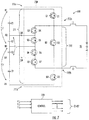
- FIG. 1 illustrates a three-level DC-DC converter apparatus 100 according to some embodiments.
- the apparatus 100 includes a string of series-connected first and second capacitors C1, C2.
- a switching circuit 110 has a first port 111 that has a first terminal 111a and a second terminals 111b that are coupled to respective first and second end nodes N1, N3 of the string of capacitors C1, C2.
- a second port 112 of the switching circuit 110 is configured to be coupled in series with first and second inductors L1, L2 and an energy storage device, here shown as a battery 10.
- the switching circuit 110 includes a plurality of switches, here shown as first through seventh insulated gate bipolar transistors (IGBTs) Q1-Q5 having associated first through seventh parallel-connected diodes D1-D5.
- the transistors Q1-Q5 are configured to selectively couple first and second terminals 112a, 112b of the second port 112 to the end nodes N1, N3 and a midpoint interconnection node N2 of the string of capacitors C1, C2.
- the first transistor Q1 is configured to connect the first terminal 111a of the first port 111 to the first terminal 112a of the second port 112.
- the second transistor Q2 is configured to connect the first terminal 112a of the second port 112 to the second terminal 112b of the second port 112.
- the third transistor Q3 is configured to connect the second terminal 111b of the first port 111 to the second terminal 112b of the second port.
- the fourth transistor Q4 is configured to connect the first terminal 112a of the second port 112 to the midpoint interconnection node N2.
- the fifth transistor Q5 is configured to connect the second terminal 112b of the second port 112 to the midpoint interconnection node N2,
- a control circuit 120 controls the transistors Q1-Q5 responsive to voltages v 1 , v 2 across respective ones of the capacitors C1, C2.
- FIGs. 2 and 3 illustrate operations of the converter apparatus 100 of FIG. 1 according to some embodiments.
- the apparatus 110 transfers power from the battery 10 by charging the inductors L1, L2 and selectively discharging the inductors L1, L2 into the first and second capacitors C1, C2 to regulate the capacitor voltages v 1 , v 2 .
- the control circuit 120 turns on (closes) the second transistor Q2, while the first transistor Q1, the third transistor Q3, the fourth transistor Q4 and the fifth transistor Q5 are off. This causes a first current 101 to flow through the first and second inductors L1, L2, thus charging the inductors L1, L2.
- the fourth transistor Q4 and the fifth transistor Q5 may be selectively turned on to provide additional current to selectively charge the first and second capacitors C1, C2 from the charged first and second inductors L1, L2.
- the capacitor voltages v 1 , v 2 are at desirable levels (in this case, substantially the same)
- the first and second capacitors C1, C2 may be simultaneously charged by a second current 102 passing through the first diode D1 and the third diode D3.
- the first capacitor C1 may be selectively (preferentially) charged by turning on the fifth transistor Q5 to enable an additional third current 103 that results in charging the first capacitor C1 more than the second capacitor C2.
- the second capacitor C2 may be selectively charged by turning on the fourth transistor Q4 to enable an additional fourth current 104 that causes the second capacitor C2 to charge more than the first capacitor C1.
- the first transistor Q1 and the third transistor Q3 may be turned on to provide a fifth current 105 that charges the first and second inductors L1, L2.
- a sixth current 106 from discharging of the inductors L1, L2 freewheels through the second diode D2, thus charging the battery 10.
- the configuration of the apparatus 100 allows for the use of different voltage ratings among the transistors Q1-Q5.
- the fourth transistor Q4 and the fifth transistor Q5 may have lower voltage ratings than the first transistor Q1, the second transistor Q2 and the third transistor Q3.
- the DC link may have a tendency towards imbalance.
- Different types of imbalances can occur, including an imbalance of the "positive” capacitors and the “negative” capacitors, which can occur when a half-wave rectified load is applied to the inverter.
- Another type of imbalance is an imbalance of the inner capacitors with respect to the outer capacitors, which may occur due to high crest factor loads on the inverter.
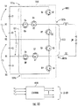
- FIG. 4 illustrates a five-level DC-DC converter apparatus 400 according to further embodiments that can be used to provide link balancing for such applications.
- the apparatus 400 includes a string of series-connected first, second, third and fourth capacitors C1, C2, C3, C4.
- a switching circuit 410 has a first port 411 that has a first terminal 41 1a and a second terminal 411b that are coupled to respective first and second end nodes N1, N5 of the string of capacitors C1-C4.
- a second port 412 of the switching circuit 410 is configured to be coupled in series with first and second inductors L1, L2 and an energy storage device, here shown as a battery 10.
- the switching circuit 410 includes a plurality of switches, here shown as including first through seventh IGBts Q1-Q7 having associated first through seventh parallel connected diodes D1-D7.
- the first transistor Q1 is configured to connect the first terminal 411a of the first port 411 to the first terminal 412a of the second port 412.
- the second transistor Q2 is configured to connect the first terminal 412a of the second port 412 to the second terminal 412b of the second port 412.
- the third transistor Q3 is configured to connect the second terminal 411b of the first port 411 to the second terminal 412b of the second port 412.
- the fourth transistor Q4 and the fifth transistor Q5 act as a bidirectional switch configured to connect the first terminal 412a of the second port 412 to an interconnection node N2.
- the sixth transistor Q5 and the seventh transistor Q7 act as a bidirectional switch configured to connect the second terminal 412b of the second port 412 to a midpoint interconnection node N4.
- a control circuit 420 controls the transistors Q1-Q7 responsive to a voltage v across the second capacitor C2 and the third capacitor C3.
- the fourth transistor Q4, the fifth transistor Q5, the sixth transistor Q6 and the seventh transistor Q7 may have a lower voltage rating than the first transistor Q1, the second transistor Q2 and the third transistor Q3.
- FIGs. 5 and 6 illustrate operations of the converter apparatus 400 of FIG. 4 for balancing capacitor voltages according to some embodiments.
- the control circuit 120 turns on the second transistor Q2 to causes a first current 401 to flow through the first and second inductors L1, L2, thus charging the inductors L1, L2.
- the second transistor Q2 is turned off, and the fourth transistor Q4, the fifth transistor Q5, the sixth transistor Q6 and the seventh transistor Q7 may be selectively turned on to selectively charge the capacitors C1-C4 from the charged first and second inductors L1, L2.
- the capacitors C1-C4 may be simultaneously charged by a second current 402 passing through the first diode D1 and the third diode D3 with all of the transistors Q1-Q7 off.
- the second capacitor C2 and the third capacitor C3 may be selectively charged by turning on the fourth transistor Q4, the fifth transistor Q5, the sixth transistor Q6 and the seventh transistor Q7 to cause a third current 403 to boost the voltage v 2 across the second capacitor C2 and the third capacitor C3.
- the first transistor Q1 and the third transistor Q3 are turned on to conduct a fourth current 404 that charges the first and second inductors L1, L2.
- the transistors Q1-Q7 are turned off and a fifth current 405 freewheels through the second diode D2, thus charging the battery 10.
- FIG. 7 illustrates a five-level DC-DC converter apparatus 700 according to further embodiments which can provide enhanced balancing capabilities.
- the apparatus 500 includes a string of series-connected first, second, third and fourth capacitors C1, C2, C3, C4.
- a switching circuit 710 has a first port 711 that has a first terminal 711a and a second terminal 711b that are coupled to respective first and second end nodes N1, N5 of the string of capacitors C1-C4.
- a second port 712 of the switching circuit 710 is configured to be coupled in series with first and second inductors L1, L2 and an energy storage device, here shown as a battery 10.
- the switching circuit 710 includes a plurality of switches, here shown as including first through seventh insulated gate bipolar transistors (IGBTs) Q1-Q7 and associated first through seventh parallel-connected diodes D1-D7, along with additional eighth and ninth diodes D8, D9.
- the first transistor Q1 is configured to connect the first terminal 711a of the first port 711 to the first terminal 712a of the second port 712.
- the second transistor Q2 is configured to connect the first terminal 712a of the second port 712 to the second terminal 712b of the second port 712.
- the third transistor Q3 is configured to connect the second terminal 711b of the first port 711 to the second terminal 712b of the second port 712.
- the fourth transistor Q4 is configured to couple the first terminal 712a of the second port 712 to the first interconnection node N2 via the eighth diode D8.
- the fifth transistor Q5 is configured to connect an emitter terminal of the fourth transistor Q4 to the midpoint interconnection node N3.
- the seventh transistor Q7 is configured to connect the second terminal 712b of the second port 712 to the interconnection node N4.
- the sixth transistor Q6 is configured to connect a collector terminal of the seventh transistor Q7 to the midpoint interconnection node N3.
- a control circuit 720 controls the transistors Q1-Q7 responsive to a voltage v 1 across the first capacitor C1 and the second capacitor C2, a voltage v 2 across the third capacitor C3 and the fourth capacitor C4, and a voltage v 3 across the second capacitor C2 and the third capacitor C3.
- the fourth transistor Q4, the fifth transistor Q5, the sixth transistor Q6 and the seventh transistor Q7 may have a lower voltage rating than the first transistor Q1, the second transistor Q2 and the third transistor Q3.
- FIGs. 8 and 9 illustrate operations of the converter apparatus 700 according to some embodiments.
- the control circuit 720 turns on the second transistor Q2 to conduct a first current 701 that flows through the first and second inductors L1, L2, thus charging the inductors L1, L2.
- the second transistor Q2 is turned off, and the fourth transistor Q4, the fifth transistor Q5, the sixth transistor Q6 and the seventh transistor Q7 can be selectively turned on to selectively charge the capacitors C1-C4 from the charged first and second inductors L1, L2.
- the capacitors C1-C4 may be simultaneously charged by a second current 702 passing through the first diode D1 and the third diode D3. If the voltage v 3 is low, the second capacitor C2 and the third capacitor C3 may be charged by turning on the fourth transistor Q4, the fifth transistor Q5, the sixth transistor Q6 and the seventh transistor Q7 to conduct a third current 703 that charges the second capacitor C2 and the third capacitor C3.
- the apparatus 700 turns on the first transistor Q1 and the third transistor Q3 to conduct a sixth current 706 that charges the first and second inductors L1, L2. In succeeding second intervals, the transistors are turned off and a seventh current 707 freewheels through the second diode D2, thus charging the battery 10.
- FIG. 10 illustrates a five-level DC-DC converter apparatus 1000 according to further embodiments.
- the apparatus 1000 includes a string of series-connected first, second, third and fourth capacitors C1, C2, C3, C4.
- a switching circuit 1010 has a first port 1011 that has a first terminal 1011a and a second terminal 1011b that are coupled to respective first and second end nodes N1, N5 of the string of capacitors C1-C4.
- a second port 1012 of the switching circuit 1010 is configured to be coupled in series with first and second inductors L1, L2 and an energy storage device, here shown as a battery 10.
- the switching circuit 1010 includes a plurality of switches, here shown as including first through eighth IGBTs Q1-Q8 having associated first through eighth parallel-connected diodes D1-D8.
- the first transistor Q1 is configured to connect the first terminal 1011a of the first port 1011 to the first terminal 1012a of the second port 1012.
- the second transistor Q2 is configured to connect the first terminal 1012a of the second port 1012 to a midpoint interconnection node N3.
- the third transistor Q3 is configured to connect the second terminal 1012b of the second port 1012 to the midpoint interconnection node N3.
- the fourth transistor Q4 is configured to connect the second terminal 1011b of the first port 101 1 to the second terminal 1012b of the second port 1012.
- the fifth transistor Q5 and the sixth transistor Q6 act as a bidirectional switch configured to connect the first terminal 1012a of the second port 1012 to an interconnection node N2.
- the seventh transistor Q7 and the eight transistor Q8 act as a bidirectional switch configured to connect the second terminal 1012b of the second port to an interconnection node N4.
- a control circuit 1020 controls the transistors Q1-Q7 responsive to a voltage v 1 across the first capacitor C1 and the second capacitor C2 , a voltage v 2 across the third capacitor C3 and the fourth capacitor C4, and a voltage v 3 across the second capacitor C2 and the third capacitor C3.
- the second transistor Q2, the third transistor Q3, the fifth transistor Q5, the sixth transistor Q6, the seventh transistor Q7, and the eighth transistor Q8 may have a lower voltage rating than the first transistor Q1 and the fourth transistor Q4.
- FIGs. 11 and 12 illustrate operations of the converter apparatus 1000 according to some embodiments.
- the control circuit 1020 turns on the second transistor Q2 and the third transistor Q3 to conduct a first current 1001 through the first and second inductors L1, L2, thus charging the inductor L1, L2.
- the second transistor Q2, the third transistor Q3, the fifth transistor Q5, the sixth transistor Q6, the seventh transistor Q7, and the eighth transistor Q8 can be selectively turned on to selectively charge the capacitors C1-C4 from the charged first and second inductors L1, L2.
- the capacitors C1-C4 may be simultaneously charged by a second current 1002 passing through the first diode D1 and the fourth diode D4. If the voltage v 3 requires boosting, the second capacitor C2 and the third capacitor C3 may be charged by turning on the fifth transistor Q5, the sixth transistor Q6, the seventh transistor Q7, and the eighth transistor Q8 to conduct a third current 1003. If the voltage v 1 requires boosting, the first capacitor C1 and the second capacitor C2 can be charged by turning on the third transistor Q3 to conduct a fourth current 1004.
- the third capacitor C3 and the fourth capacitor C4 can be charged by turning on the second transistor Q2 to conduct a fifth current 1005.
- the apparatus 1000 turns on the first transistor Q1 and the fourth transistor Q4 to conduct a sixth current 1006 that charges the first and second inductors L1, L2, and then the transistors are turned off and a seventh current 1007 freewheels through the second diode D2 and the third diode D3 to charge the battery 10.
- FIG. 13 illustrates a five-level DC-DC converter apparatus 1300 according to still further embodiments.
- the apparatus 500 includes a string of series-connected first, second, third and fourth capacitors C1, C2, C3, C4.
- a switching circuit 1310 has a first port 1311 that has a first terminal 1311a and a second terminal 1311b that are coupled to respective first and second end nodes N1, N5 of the string of capacitors C1-C4.
- a second port 1312 of the switching circuit 1310 is configured to be coupled in series with first and second inductors L1, L2 and an energy storage device, here shown as a battery 10.
- the switching circuit 1310 includes a plurality of switches, here shown as including first through sixth IGBTs Q1-Q6 having associated first through sixth parallel connected diodes D1-D6, along with additional seventh and eighth diodes D7, D8.
- the first transistor Q1 is configured to connect the first terminal 1311a of the first port 1311 to the first terminal 1312a of the second port 1312.
- the sixth transistor Q6 is configured to connect the second terminal 1311b of the first port 1311 to the second terminal 1312b of the second port 1312.
- the second transistor Q2 is configured to couple the first terminal 1312a of the second port 1312 to a first interconnection node N2 via the seventh diode D7.
- the third transistor Q3 is configured to connect an emitter terminal of the second transistor Q2 to a midpoint interconnection node N3.
- the fifth transistor Q5 is configured to connect the second terminal 1312b of the second port 1312 to an interconnection node N4 via the eighth diode D8.
- the fourth transistor Q4 is configured to connect a collector terminal of the fifth transistor Q5 to the midpoint interconnection node N3.
- a control circuit 1320 controls the transistors Q1-Q6 responsive to a voltage v 1 across the first capacitor C1 and the second capacitor C2, a voltage v 2 across the third capacitor C3 and the fourth capacitor C4, and a voltage v 3 across the second capacitor C2 and the third capacitor C3.
- the second transistor Q2, the third transistor Q3, the fourth transistor Q4 and the fifth transistor Q5 may have a lower voltage rating than the first transistor Q1 and the sixth transistor Q6.
- FIGs. 14 and 15 illustrate operations of the converter apparatus 1300 according to some embodiments.
- the control circuit 1320 turns on the second transistor Q2, the third transistor Q3, the fourth transistor Q4, and the fifth transistor Q5 to conduct a first current 1301 that charges the first and second inductors L1, L2.
- the transistors Q1-Q6 can be selectively turned on to selectively charge the capacitors C1-C4 from the charged first and second inductors L1, L2.
- the capacitors C1-C4 may be simultaneously charged by a second current 1302 passing through the first diode D1 and the sixth diode D6. If the voltage v 3 requires boosting, the second capacitor C2 and the third capacitor C3 may be charged by turning on the second transistor Q2 and the fifth transistor Q5 to conduct a third current 1303. If the voltage v 1 requires boosting, the first capacitor C1 and the second capacitor C2 can be charged by turning on the fourth transistor Q4 and the fifth transistor Q5 to conduct a fourth current 1304.
- the third capacitor C3 and the fourth capacitor C4 can be charged by turning on the second transistor Q2 and the third transistor Q3 to conduct a fifth current 1305.
- the apparatus 1300 turns on the first transistor Q1 and the sixth transistor Q6 to conduct a sixth current 1306 that charges the first and second inductors L1, L2.
- the transistors Q1-Q6 are all turned off and seventh current 1307 freewheels through the second diode D2, the third diode D3, the fourth diode D4 and the fifth diode D5 to charge the battery 10.
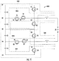
- FIG. 16 illustrates a five-level DC-DC converter apparatus 1600 according to further embodiments.
- the apparatus 1600 includes a string of series-connected first, second, third and fourth capacitors C1, C2, C3, C4.
- a switching circuit 1610 has a first port 1611 that has a first terminal 1611a and a second terminal 1611b that are coupled to respective first and second end nodes N1, N5 of the string of capacitors C1-C4.
- a second port 1612 of the switching circuit 1610 is configured to be coupled in series with first and second inductors L1, L2 and an energy storage device, here shown as a battery 10.
- the switching circuit 1610 includes a plurality of switches, here shown as including first through ninth IGBTs Q1-Q8 having associated first through ninth parallel-connected diodes D1-D9.
- the first transistor Q1 is configured to connect the first terminal 1611a of the first port 1611 to the first terminal 1612a of the second port 1612.
- the second transistor Q2 is configured to connect the first terminal 1612a of the second port 1612 to a midpoint interconnection node N3.
- the third transistor Q3 is configured to connect the second terminal 1612b of the second port 1612 to the midpoint interconnection node N3.
- the fourth transistor Q4 is configured to connect the second terminal 1611b of the first port 1611 to the second terminal 1612b of the second port 1612.
- the fifth transistor Q5 and the sixth transistor Q6 act as a bidirectional switch configured to connect the first terminal 1612a of the second port 1612 to an interconnection node N2.
- the seventh transistor Q7 and the eight transistor Q8 act as a bidirectional switch configured to connect the second terminal 1612b of the second port to an interconnection node N4.
- the ninth transistor Q9 connects the first terminal 1612a of the second port 1612 directly to the second terminal 1612b of the second port 1612.
- a control circuit 1620 controls the transistors Q1-Q9 responsive to a voltage v 1 across the first capacitor C1 and the second capacitor C2 , a voltage v 2 across the third capacitor C3 and the fourth capacitor C4, and a voltage v 3 across the second capacitor C2 and the third capacitor C3.
- the second transistor Q2, the third transistor Q3, the fifth transistor Q5, the sixth transistor Q6, the seventh transistor Q7, and the eighth transistor Q8 may have a lower voltage rating than the first transistor Q1, the fourth transistor Q4 and the ninth transistor Q9.
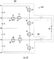
- FIGs. 17 and 18 illustrate operations of the converter apparatus 1600 according to some embodiments.
- the control circuit 1620 turns on the ninth transistor Q9 to conduct a first current 1601 through the first and second inductors L1, L2, thus charging the inductor L1, L2.
- the second transistor Q2, the third transistor Q3, the fifth transistor Q5, the sixth transistor Q6, the seventh transistor Q7, and the eighth transistor Q8 can be selectively turned on to selectively charge the capacitors C1-C4 from the charged first and second inductors L1, L2.
- the capacitors C1-C4 may be simultaneously charged by a second current 1602 passing through the first diode D1 and the fourth diode D4. If the voltage v 3 requires boosting, the second capacitor C2 and the third capacitor C3 may be charged by turning on the fifth transistor Q5, the sixth transistor Q6, the seventh transistor Q7, and the eighth transistor Q8 to conduct a third current 1603. If the voltage v 1 requires boosting, the first capacitor C1 and the second capacitor C2 can be charged by turning on the third transistor Q3 to conduct a fourth current 1604.
- the third capacitor C3 and the fourth capacitor C4 can be charged by turning on the second transistor Q2 to conduct a fifth current 1605.
- the apparatus 1600 turns on the first transistor Q1 and the fourth transistor Q4 to conduct a sixth current 1606 that charges the first and second inductors L1, L2, and then the transistors are turned off and a seventh current 1607 freewheels through the ninth diode D9 to charge the battery 10.
- DC-DC converter apparatus may be advantageously used in paralleled multi-level inverter applications.
- parallel-connected UPSs 1900 may each include multi-level inverters 1920 that are connected in common to a load 20.
- Respective balancing multi-level DC-DC converters 1910 along lines discussed above may couple the multi-level inverters 1920 to respective DC sources 10, such as batteries, capacitor banks and/or fuel cells.
- DC sources 10 such as batteries, capacitor banks and/or fuel cells.
- Such an arrangement can be used to reduce or eliminate circulating currents among the UPSs 1900, as the balancing multi-level DC-DC converters 1910 can equalize the DC voltages applied to the multi-level inverters 1920.
- Similar arrangements may be used other inverter-paralleling applications, such as in grid-tied energy storage applications, motor drives and the like.
Landscapes
- Engineering & Computer Science (AREA)
- Power Engineering (AREA)
- Dc-Dc Converters (AREA)
- Inverter Devices (AREA)
Applications Claiming Priority (1)
| Application Number | Priority Date | Filing Date | Title |
|---|---|---|---|
| US16/549,867 US11088615B2 (en) | 2019-08-23 | 2019-08-23 | Balancing multilevel DC-DC converter apparatus |
Publications (3)
| Publication Number | Publication Date |
|---|---|
| EP3783784A2 true EP3783784A2 (fr) | 2021-02-24 |
| EP3783784A3 EP3783784A3 (fr) | 2021-03-10 |
| EP3783784B1 EP3783784B1 (fr) | 2026-03-04 |
Family
ID=72178367
Family Applications (1)
| Application Number | Title | Priority Date | Filing Date |
|---|---|---|---|
| EP20191834.9A Active EP3783784B1 (fr) | 2019-08-23 | 2020-08-19 | Équilibrage d'appareil convertisseur cc-cc à plusieurs niveaux |
Country Status (3)
| Country | Link |
|---|---|
| US (1) | US11088615B2 (fr) |
| EP (1) | EP3783784B1 (fr) |
| CN (1) | CN112421947B (fr) |
Cited By (2)
| Publication number | Priority date | Publication date | Assignee | Title |
|---|---|---|---|---|
| US20220045609A1 (en) * | 2018-07-11 | 2022-02-10 | Maxim Integrated Products, Inc. | Charging Device |
| EP4503413A1 (fr) * | 2023-08-01 | 2025-02-05 | Delta Electronics Inc. | Convertisseur de puissance et procédé de conversion de puissance capable d'équilibrer l'énergie et alimentation électrique hybride |
Families Citing this family (4)
| Publication number | Priority date | Publication date | Assignee | Title |
|---|---|---|---|---|
| US11294438B2 (en) * | 2020-04-29 | 2022-04-05 | Dell Products L.P. | System and method of providing power from one portion of an information handling system to another portion of the information handling system |
| US10965221B1 (en) * | 2020-09-01 | 2021-03-30 | King Abdulaziz University | Switched capacitor based boost inverter topology with a higher number of levels and higher voltage gain |
| CN114094839B (zh) * | 2022-01-11 | 2022-04-08 | 四川大学 | 一种电感储能型隔离式dc-dc变换器及其控制方法 |
| US12483136B2 (en) * | 2022-11-04 | 2025-11-25 | University Of North Texas | Multiple port bidirectional power conversion circuit |
Citations (3)
| Publication number | Priority date | Publication date | Assignee | Title |
|---|---|---|---|---|
| US6819576B2 (en) | 1999-08-13 | 2004-11-16 | Powerware Corporation | Power conversion apparatus and methods using balancer circuits |
| US20180275699A1 (en) | 2017-03-23 | 2018-09-27 | Eaton Corporation | Power converter apparatus and methods using adaptive node balancing |
| US20180278074A1 (en) | 2017-03-23 | 2018-09-27 | Eaton Intelligent Power Limited | Auto adjusting balancer apparatus |
Family Cites Families (16)
| Publication number | Priority date | Publication date | Assignee | Title |
|---|---|---|---|---|
| JPH05276756A (ja) * | 1992-03-26 | 1993-10-22 | Toshiba Lighting & Technol Corp | 電源装置、放電灯点灯装置および照明装置 |
| TWI297975B (en) * | 2005-07-26 | 2008-06-11 | Delta Electronics Inc | Integrated converter having three-phase power factor correction |
| US7705489B2 (en) * | 2006-09-08 | 2010-04-27 | American Power Conversion Corporation | Method and apparatus for providing uninterruptible power |
| JP2008289266A (ja) * | 2007-05-17 | 2008-11-27 | Mitsubishi Electric Corp | Dc/dc電力変換装置 |
| TWI367619B (en) * | 2008-09-01 | 2012-07-01 | Delta Electronics Inc | Parallel-connectred uninterrupted power supply circuit |
| TWI390827B (zh) * | 2008-09-22 | 2013-03-21 | Ablerex Electronics Co Ltd | 具中性點之雙向直流/直流電壓轉換裝置及應用該電壓轉換裝置的不斷電系統 |
| US8513928B2 (en) * | 2011-01-05 | 2013-08-20 | Eaton Corporation | Bidirectional buck-boost converter |
| CN102244477A (zh) * | 2011-07-07 | 2011-11-16 | 西南交通大学 | 具有直流电容辅助均压电路的多电平变换器 |
| US8884464B2 (en) * | 2011-08-29 | 2014-11-11 | Schneider Electric It Corporation | Twin boost converter with integrated charger for UPS system |
| US8981843B2 (en) * | 2012-05-31 | 2015-03-17 | Fairchild Semiconductor Corporation | Translator including overstress protection |
| US9564806B2 (en) * | 2013-09-25 | 2017-02-07 | Cree, Inc. | Boost converter with reduced switching loss and methods of operating the same |
| US20150131349A1 (en) | 2013-11-12 | 2015-05-14 | General Electric Company | System and method for balancing multilevel power converters |
| US9935549B2 (en) | 2016-07-08 | 2018-04-03 | Toshiba International Corporation | Multi-switch power converter |
| US10447052B2 (en) | 2017-03-23 | 2019-10-15 | Intel Corporation | Apparatus, method, and system for dynamically controlling current and/or voltage profiles |
| CN207504780U (zh) * | 2017-10-30 | 2018-06-15 | 西南交通大学 | 一种五电平变换器的均压电路 |
| US20190199226A1 (en) * | 2017-12-22 | 2019-06-27 | Xiamen Kehua Hengsheng Limited By Share Ltd. | Voltage converting device and method of controlling the voltage converting device |
-
2019
- 2019-08-23 US US16/549,867 patent/US11088615B2/en active Active
-
2020
- 2020-08-19 EP EP20191834.9A patent/EP3783784B1/fr active Active
- 2020-08-24 CN CN202010854160.8A patent/CN112421947B/zh active Active
Patent Citations (3)
| Publication number | Priority date | Publication date | Assignee | Title |
|---|---|---|---|---|
| US6819576B2 (en) | 1999-08-13 | 2004-11-16 | Powerware Corporation | Power conversion apparatus and methods using balancer circuits |
| US20180275699A1 (en) | 2017-03-23 | 2018-09-27 | Eaton Corporation | Power converter apparatus and methods using adaptive node balancing |
| US20180278074A1 (en) | 2017-03-23 | 2018-09-27 | Eaton Intelligent Power Limited | Auto adjusting balancer apparatus |
Cited By (4)
| Publication number | Priority date | Publication date | Assignee | Title |
|---|---|---|---|---|
| US20220045609A1 (en) * | 2018-07-11 | 2022-02-10 | Maxim Integrated Products, Inc. | Charging Device |
| US11817725B2 (en) * | 2018-07-11 | 2023-11-14 | Maxim Integrated Products, Inc. | Charging device |
| EP4503413A1 (fr) * | 2023-08-01 | 2025-02-05 | Delta Electronics Inc. | Convertisseur de puissance et procédé de conversion de puissance capable d'équilibrer l'énergie et alimentation électrique hybride |
| JP2025022766A (ja) * | 2023-08-01 | 2025-02-14 | 台達電子工業股▲ふん▼有限公司 | エネルギーバランスとハイブリッド電源を実現可能な電力変換器及び電力変換方法 |
Also Published As
| Publication number | Publication date |
|---|---|
| CN112421947B (zh) | 2026-01-23 |
| CN112421947A (zh) | 2021-02-26 |
| EP3783784B1 (fr) | 2026-03-04 |
| EP3783784A3 (fr) | 2021-03-10 |
| US20210057991A1 (en) | 2021-02-25 |
| US11088615B2 (en) | 2021-08-10 |
Similar Documents
| Publication | Publication Date | Title |
|---|---|---|
| EP3783784B1 (fr) | Équilibrage d'appareil convertisseur cc-cc à plusieurs niveaux | |
| US20220344947A1 (en) | Energy storage system, balancing control method for energy storage system, and photovoltaic power system | |
| Lu et al. | Photovoltaic-battery-powered DC bus system for common portable electronic devices | |
| CN110677060A (zh) | 功率变换系统及其中直流母线电容的预充电方法 | |
| CN106559004A (zh) | 多电平逆变器 | |
| CN115362610B (zh) | 具有多个lvdc输出的sst系统 | |
| CA3098017A1 (en) | Multi-port dc/dc converter system | |
| US20180358823A1 (en) | Flexbattery | |
| US20220158549A1 (en) | Power conversion system and control method | |
| CN111525672A (zh) | 一种多端口储能电池 | |
| KR20220029522A (ko) | 단일단 교류 직류 변환기 | |
| CN113547945A (zh) | 基于导抗网络的带均压功能的电池充电装置及方法 | |
| Cano et al. | Distributed input multiport MMC based power converter for AC and DC loads | |
| CN112671016A (zh) | 一种基于模块化的移动储能系统 | |
| Alam et al. | Pulsating power processing through multi-active bridge for electric vehicle charging applications | |
| CN118573016A (zh) | 一种集成光伏均衡器与电池均衡器的光伏储能系统一体化变换器 | |
| Hawke et al. | A multiport power sharing converter topology for renewable-to-grid interface | |
| CN205490218U (zh) | 一种具有电池能量平衡功能的单相五电平逆变器 | |
| CN219938014U (zh) | 储能模块均衡电路及电源装置 | |
| Lee et al. | A New Chain-Structured Cell-Balancing Circuit with a Coupled-Inductor Based Modules | |
| Dam et al. | A capacitively level shifted fast cell-to-cell battery voltage equalizer | |
| Wu et al. | Enhancing Battery Performance with Active Balancing and Fault Tolerance in Lead-Acid Energy Storage Systems | |
| CN215498336U (zh) | 一种储能电路 | |
| Saxena et al. | A Reconfigurable DC-DC Converter with Active Battery Charge Equalization for Power Management of Residential DC Nano-Grids | |
| CN213990170U (zh) | 基于模块化的移动储能系统 |
Legal Events
| Date | Code | Title | Description |
|---|---|---|---|
| PUAI | Public reference made under article 153(3) epc to a published international application that has entered the european phase |
Free format text: ORIGINAL CODE: 0009012 |
|
| STAA | Information on the status of an ep patent application or granted ep patent |
Free format text: STATUS: REQUEST FOR EXAMINATION WAS MADE |
|
| REG | Reference to a national code |
Ref country code: DE Ref legal event code: R079 Free format text: PREVIOUS MAIN CLASS: H02M0003145000 Ipc: H02M0003158000 |
|
| PUAL | Search report despatched |
Free format text: ORIGINAL CODE: 0009013 |
|
| 17P | Request for examination filed |
Effective date: 20200819 |
|
| AK | Designated contracting states |
Kind code of ref document: A2 Designated state(s): AL AT BE BG CH CY CZ DE DK EE ES FI FR GB GR HR HU IE IS IT LI LT LU LV MC MK MT NL NO PL PT RO RS SE SI SK SM TR |
|
| AX | Request for extension of the european patent |
Extension state: BA ME |
|
| AK | Designated contracting states |
Kind code of ref document: A3 Designated state(s): AL AT BE BG CH CY CZ DE DK EE ES FI FR GB GR HR HU IE IS IT LI LT LU LV MC MK MT NL NO PL PT RO RS SE SI SK SM TR |
|
| AX | Request for extension of the european patent |
Extension state: BA ME |
|
| RIC1 | Information provided on ipc code assigned before grant |
Ipc: H02M 3/158 20060101AFI20210129BHEP |
|
| P01 | Opt-out of the competence of the unified patent court (upc) registered |
Effective date: 20230521 |
|
| GRAP | Despatch of communication of intention to grant a patent |
Free format text: ORIGINAL CODE: EPIDOSNIGR1 |
|
| STAA | Information on the status of an ep patent application or granted ep patent |
Free format text: STATUS: GRANT OF PATENT IS INTENDED |
|
| INTG | Intention to grant announced |
Effective date: 20250926 |
|
| GRAS | Grant fee paid |
Free format text: ORIGINAL CODE: EPIDOSNIGR3 |
|
| GRAA | (expected) grant |
Free format text: ORIGINAL CODE: 0009210 |
|
| STAA | Information on the status of an ep patent application or granted ep patent |
Free format text: STATUS: THE PATENT HAS BEEN GRANTED |
|
| AK | Designated contracting states |
Kind code of ref document: B1 Designated state(s): AL AT BE BG CH CY CZ DE DK EE ES FI FR GB GR HR HU IE IS IT LI LT LU LV MC MK MT NL NO PL PT RO RS SE SI SK SM TR |
|
| REG | Reference to a national code |
Ref country code: CH Ref legal event code: F10 Free format text: ST27 STATUS EVENT CODE: U-0-0-F10-F00 (AS PROVIDED BY THE NATIONAL OFFICE) Effective date: 20260304 Ref country code: GB Ref legal event code: FG4D |
|
| REG | Reference to a national code |
Ref country code: IE Ref legal event code: FG4D |
|
| REG | Reference to a national code |
Ref country code: DE Ref legal event code: R096 Ref document number: 602020067858 Country of ref document: DE |