EP3783339B1 - Detektorzelle für einen photo-akustischen gassensor sowie photo-akustischer gassensor - Google Patents
Detektorzelle für einen photo-akustischen gassensor sowie photo-akustischer gassensor Download PDFInfo
- Publication number
- EP3783339B1 EP3783339B1 EP19193158.3A EP19193158A EP3783339B1 EP 3783339 B1 EP3783339 B1 EP 3783339B1 EP 19193158 A EP19193158 A EP 19193158A EP 3783339 B1 EP3783339 B1 EP 3783339B1
- Authority
- EP
- European Patent Office
- Prior art keywords
- layer structure
- cavity
- detector cell
- layer
- sub
- Prior art date
- Legal status (The legal status is an assumption and is not a legal conclusion. Google has not performed a legal analysis and makes no representation as to the accuracy of the status listed.)
- Active
Links
Images









Classifications
-
- G—PHYSICS
- G01—MEASURING; TESTING
- G01N—INVESTIGATING OR ANALYSING MATERIALS BY DETERMINING THEIR CHEMICAL OR PHYSICAL PROPERTIES
- G01N21/00—Investigating or analysing materials by the use of optical means, i.e. using sub-millimetre waves, infrared, visible or ultraviolet light
- G01N21/17—Systems in which incident light is modified in accordance with the properties of the material investigated
- G01N21/1702—Systems in which incident light is modified in accordance with the properties of the material investigated with opto-acoustic detection, e.g. for gases or analysing solids
-
- G—PHYSICS
- G01—MEASURING; TESTING
- G01N—INVESTIGATING OR ANALYSING MATERIALS BY DETERMINING THEIR CHEMICAL OR PHYSICAL PROPERTIES
- G01N29/00—Investigating or analysing materials by the use of ultrasonic, sonic or infrasonic waves; Visualisation of the interior of objects by transmitting ultrasonic or sonic waves through the object
- G01N29/22—Details, e.g. general constructional or apparatus details
- G01N29/24—Probes
- G01N29/2418—Probes using optoacoustic interaction with the material, e.g. laser radiation, photoacoustics
- G01N29/2425—Probes using optoacoustic interaction with the material, e.g. laser radiation, photoacoustics optoacoustic fluid cells therefor
-
- G—PHYSICS
- G01—MEASURING; TESTING
- G01N—INVESTIGATING OR ANALYSING MATERIALS BY DETERMINING THEIR CHEMICAL OR PHYSICAL PROPERTIES
- G01N33/00—Investigating or analysing materials by specific methods not covered by groups G01N1/00 - G01N31/00
- G01N33/0004—Gaseous mixtures, e.g. polluted air
- G01N33/0009—General constructional details of gas analysers, e.g. portable test equipment
- G01N33/0027—General constructional details of gas analysers, e.g. portable test equipment concerning the detector
- G01N33/0036—General constructional details of gas analysers, e.g. portable test equipment concerning the detector specially adapted to detect a particular component
- G01N33/004—CO or CO2
-
- G—PHYSICS
- G01—MEASURING; TESTING
- G01N—INVESTIGATING OR ANALYSING MATERIALS BY DETERMINING THEIR CHEMICAL OR PHYSICAL PROPERTIES
- G01N21/00—Investigating or analysing materials by the use of optical means, i.e. using sub-millimetre waves, infrared, visible or ultraviolet light
- G01N21/17—Systems in which incident light is modified in accordance with the properties of the material investigated
- G01N21/1702—Systems in which incident light is modified in accordance with the properties of the material investigated with opto-acoustic detection, e.g. for gases or analysing solids
- G01N2021/1704—Systems in which incident light is modified in accordance with the properties of the material investigated with opto-acoustic detection, e.g. for gases or analysing solids in gases
-
- G—PHYSICS
- G01—MEASURING; TESTING
- G01N—INVESTIGATING OR ANALYSING MATERIALS BY DETERMINING THEIR CHEMICAL OR PHYSICAL PROPERTIES
- G01N21/00—Investigating or analysing materials by the use of optical means, i.e. using sub-millimetre waves, infrared, visible or ultraviolet light
- G01N21/17—Systems in which incident light is modified in accordance with the properties of the material investigated
- G01N21/1702—Systems in which incident light is modified in accordance with the properties of the material investigated with opto-acoustic detection, e.g. for gases or analysing solids
- G01N2021/1708—Systems in which incident light is modified in accordance with the properties of the material investigated with opto-acoustic detection, e.g. for gases or analysing solids with piezotransducers
-
- G—PHYSICS
- G01—MEASURING; TESTING
- G01N—INVESTIGATING OR ANALYSING MATERIALS BY DETERMINING THEIR CHEMICAL OR PHYSICAL PROPERTIES
- G01N2223/00—Investigating materials by wave or particle radiation
- G01N2223/50—Detectors
- G01N2223/508—Detectors photo-acoustic
Definitions
- the present disclosure is related to a detector cell for a photoacoustic gas sensor, to photoacoustic gas sensors and to methods for fabricating a detector cell and a photoacoustic gas sensor.
- the present disclosure further relates to a wafer level bonded photoacoustic detector cell.
- Photoacoustic gas sensors may be used to measure environmental conditions, for example, portions of a fluid, in particular a gas.
- US 2016/282259 A1 relates to a gas sensor including a sensor element, a measurement chamber and an emitter element.
- the sensor element has a MEMS membrane which is arranged in a first substrate region.
- the measurement chamber is embodied to receive a measurement gas.
- WO 2017/207399 A1 relates to a microelectronic sensor device and a corresponding method for producing a microelectronic sensor device.
- the microelectronic sensor device comprises an infrared source and a pressure-sensitive micromembrane, wherein a gas chamber having a specific gas is arranged on a top side of the pressure-sensitive micromembrane.
- a detector cell for a photoacoustic gas sensor as defined with independent claim 1.
- the detector cell comprises a first layer structure, a second layer structure arranged at the first layer structure and comprising a membrane structure and comprises a third layer structure arranged at the second layer structure.
- the first layer structure and the third layer structure hermetically enclose a cavity, wherein the membrane structure is arranged in the cavity.
- the sealing to hermetically enclose the cavity may have a high durability and a high robustness.
- a coating layer reflective for electromagnetic radiation is arranged at a surface of the first layer structure facing the membrane structure or at a surface of the third layer structure facing the membrane structure.
- An embodiment provides for a photoacoustic gas sensor comprising such a detector cell and comprising an electromagnetic source configured for emitting an electromagnetic radiation so as to excite a movement of the membrane structure based on an asymmetric energy absorption of the electromagnetic radiation in different sub-cavities of the cavity, the different sub-cavities arranged on different sides of the membrane structure.
- Embodiments provide for a chip-scaled packaged photoacoustic gas sensors comprising a detector cell having a membrane structure inside a detector cell cavity, having a first sub-cavity of the cavity at a first side of the membrane structure and having a second sub-cavity of the cavity at a second, opposing side of the membrane structure.
- the chip-scaled packaged photoacoustic gas sensor comprises an electromagnetic source configured for emitting an electromagnetic radiation so as to excite a movement of the membrane structure based on a asymmetric energy absorption of the electromagnetic radiation in the first sub-cavity and the second sub-cavity.
- a method for manufacturing a detector cell as defined with independent claim 17. comprises providing a first layer structure, attaching a second layer structure having a membrane structure at the first layer structure and attaching a third layer structure at the second layer structure. The method is carried out such that the first layer structure and the third layer structure hermetically enclose a cavity and such that the membrane structure is arranged in the cavity.
- a coating layer reflective for electromagnetic radiation is arranged at a surface of the first layer structure facing the membrane structure or at a surface of the third layer structure facing the membrane structure.
- An embodiment provides for a method for manufacturing a photoacoustic gas sensor.
- the method comprises providing a detector cell having a membrane structure inside a detector cell cavity, a first sub-cavity of the cavity at a first side of the membrane structure, and a second sub-cavity of the cavity at a second, opposing side of the membrane structure.
- the method comprises arranging an electromagnetic source configured for emitting an electromagnetic radiation so as to excite a movement of the membrane structure based on an asymmetric energy absorption of the electromagnetic radiation in the first sub-cavity and the second sub-cavity.
- Embodiments described herein relate to photoacoustic gas sensors and to detector cells that may be used in such photoacoustic gas sensors.
- a photoacoustic gas sensor may comprise a detector cell in which a target gas, i.e., molecules or same or different type, are enclosed. That is, a single gas or a combination of gases or fluids may be enclosed.
- a detector cell may be arranged in a housing of a photoacoustic gas sensor, the photoacoustic gas sensor comprising a source of electromagnetic radiation. Further details in view of a working principle of a photoacoustic gas sensor are described in connection with disclosed embodiments.
- Embodiments are related to a detector cell being a microelectromechanical structure (MEMS).
- MEMS structure may comprise one or more semiconductor materials, for example, an at least partially doped or undoped semiconductor material such as silicon, gallium, arsenide or the like. Materials derived therefrom such as a silicon nitride (SiN, Si 3 N 4 , respectively), silicon oxide (SiO 2 ) or the like may be arranged alternatively or in addition. Alternatively or in addition, other materials such as a metal material, e.g., copper, gold, silver, platinum or the like, may be part of a MEMS structure.
- a metal material e.g., copper, gold, silver, platinum or the like
- Embodiments described herein may relate to a membrane structure.
- a membrane structure may be understood as a beam-like structure (having a longitudinal extension being larger than a lateral extension perpendicular hereto), but may also be a planar or two-dimensional structure in which lateral extensions perpendicular to each other are equal with respect to each other within a tolerance range.
- An example for such a structure may be a circular structure, e.g., a round or circular membrane, or a quadratic membrane structure.
- Such a membrane structure may be formed, for example, similar to a membrane structure being used in MEMS microphones or MEMS loudspeakers.
- Fig. 1 is a schematic side view of a detector cell 10 according to an embodiment.
- the detector cell 10 may be usable or integrateable into a photoacoustic gas sensor. That is, the detector cell 10 may form a component of a photoacoustic gas sensor but may be implemented separately or individually.
- the detector cell 10 may comprise a first layer structure 12, a second layer structure 14 and a third layer structure 16 arranged as a stack of layer structures. That is, the layer structure 14 may be arranged at the layer structure 12.
- the layer structure 16 may be arranged at the layer structure 14.
- the layer structure 12 may comprise one or more layers.
- the layer structure 12 may comprise two layers 12, and 12 2 , wherein the layers 12, and 12 2 may comprise same or different materials.
- the layer structure 14 may comprise one or more layers.
- the layer structure 14 may comprise layers 14 1 and 14 2 having same or different materials.
- the layer structure 16 may comprise one or more layers.
- the layer structure 16 may comprise layers 16 1 and 16 2 having same or different materials.
- a number of layers of the layer structure 12, 14 and/or 16 may be implemented individually and equal or different with regard to a number of layers of other layer structures.
- a number of layers of each layer structure 12, 14 and 16 may be, for example, one, two, three, four, five or higher, e.g., seven or ten.
- the layer structure 14 may comprise a membrane structure 18.
- the membrane structure 18 may comprise one or more layers, for example, a semiconductor layer a semiconductor layer and a conductive layer, e.g., a doped semiconductor material or a metal material, covering at least parts of one or two sides of the membrane structure 18.
- the membrane structure 18 may be arranged such that sub-cavities 22a and 22b of a cavity 22 are arranged on different sides of the membrane structure 18.
- a recess may be implemented in the layer structure 12 and/or the layer structure 14 so as to form sub-cavity 22a.
- a recess may be formed in the layer structure 14 and/or the layer structure 16 so as to form sub-cavity 22b.
- embodiments relate to a structure having only one of sub-cavities 22a and 22b, wherein further embodiments relate to structures having sub-cavity 22a and sub-cavity 22b.
- Sub-cavity 22a may be fluidically connected to sub-cavity 22b or may be sealed from sub-cavity 22b.
- Layer structure 12 and layer structure 16 thus hermetically enclose cavity 22.
- the membrane structure 18 is arranged in the cavity.
- the layer structure 12 and the layer structure 18 may be connected to each other so as to form a hermetically tight mechanical connection.
- layer structures 14 and 16 may be connected to each other so as to form a hermetically tight mechanical connection with respect to each other. This is different when compared to a cavity in which a structure is arranged which itself hosts a cavity in which a membrane is arranged. According to embodiments, it is enabled to generate the cavity 22 directly via mechanically connecting layer structures to each other.
- the layer structure 14 may form at least a part of a sidewall 10A of the detector cell 10.
- the cavity 22 may comprise or host a fluid, for example, a gas being a target gas for a later photoacoustic gas sensor.
- Fig. 2a shows a schematic side view of a detector cell 20 according to an embodiment.
- the layer structures 12 and 16 may comprise, for example, semiconductor materials, conductive materials and/or insulating materials.
- the layer structure 12 may comprise a glass material or a ceramic material as an insulating material.
- a semiconductor material for example, a silicon material or a gallium-arsenide material may be used.
- a conductive material for example, a metal material such as gold, silver, aluminum, copper or the like, including allays, may be used.
- a doped semiconductor material may be used.
- the layer structure 12 may be obtained from a glass wafer or a silicon wafer.
- the layer structure 12 may be referred to as a bottom sealing wafer.
- the layer structure 16 may, in contrast, be referred to as a top sealing cap wafer and may comprise, for example, a semiconductor material or an insulating material.
- a semiconductor material such as silicon may allow for generating or obtaining sub-cavity 22b as a recess in the layer structure 16, whilst a glass material does not exclude such a configuration but may provide for an increased hardness of the material.
- Sub-cavity 22a may be formed at least partially as a recess in the layer structure 14.
- the layer structure 14 may comprise a structure that corresponds, essentially, to a Si-microphone structure.
- the membrane structure 18 may be a multi-layer structure.
- Layer structures 12 and 14 may be bonded to each other, for example, during a wafer bonding process.
- a boundary layer or an interface 24 may be arranged between the layer structures 12 and 14, a boundary layer or an interface 24 may be arranged.
- the interface 24 may be a result of the wafer bonding process.
- a material arranged at the layer structure 12 and a material of the layer structure 14 may each form a part of the interface 24.
- the layer structure 12 may comprise a coating layer 26 and a substrate layer 28.
- the substrate layer 28 may comprise, for example, a conductive, insulating or semiconductor material such as a silicon material.
- the coating layer 26 may be arranged, for example, comprising a metal material, e.g., a gold material, wherein, alternatively, other materials such as aluminum or other reflective metallic or non-metallic materials or structures.
- gold (Au) and aluminum (Al) may be used for implementing an Eutektik bond.
- Such a material may, at a same time, provide for reflective properties. This does not exclude to use different materials for bonding and for the reflective surface.
- a glass frit may be used for bonding.
- Any reflective structure or material may be used as coating layer 26.
- Au may be inert and optically stable.
- a Bragg mirror structure may be used.
- such a structure may be obtained from Si/SiO 2 material for the present embodiments. That is, the coating layer 26 may form a surface being reflective for electromagnetic radiation and may comprises at least one of a reflective material and a reflective structure.
- the material of the coating layer 26 and the material of the layer structure 14 may form the interface 24, thereby providing a tight mechanical connection and thus a part of the hermetic sealing.
- the coating layer 26 may, optionally, be arranged in a region of the cavity, the sub-cavity 22a and/or the sub-cavity 22b. This may allow for a reflective surface, e.g., to reflect thermal radiation or other electromagnetic radiation.
- the coating layer 26 may provide for a surface reflective for electromagnetic radiation.
- the coating layer 26 may be arranged at surface of the layer structure 12 so as to face the membrane structure 18.
- the coating layer 26 may be arranged at the layer structure 16 so as to face the membrane structure 18.
- the coating layer 26 may allow to prevent an entry of electromagnetic radiation into the shielded sub-cavity, e.g., from a bottom side of Fig. 2a .
- the coating layer 26 may allow to reflect electromagnetic radiation 54 that has already entered the cavity so as to prevent an escape of the radiation.
- a coating structure or coating layer 32 may be arranged, for example, comprising a gold material, an aluminum material or the like
- a combination of materials may be arranged, e.g., gold/tin (AuSn).
- AuSn gold/tin
- Embodiments relate to host a target medium such as a fluid, e.gt., a gas as illustrated by example molecules 34 1 to 34 i in the cavity.
- a target medium may be, for example, CO 2 , CO, NO 2 or any other suitable fluid such as CH 4 (Methane) and SO 2 .
- the membrane structure 18 may comprise connections between sub-cavity 22a and sub-cavity 22b, for example, implemented by ventilation holes 36 1 and 36 2 , wherein a number of ventilation holes may be different, for example, 0, 1, 3 or more, 5 or more, 10 or more, 20 or more, or even higher numbers. This may allow to obtain a connection between the layer structures 12 and 14 and/or between the layer structures 14 and 16 differently.
- the layer structures 12 and 14 and/or the layer structures 14 and 16 may be formed as a common layer structure out of which a respective sub-cavity 22a or 22b is formed, for example, using an etching process. This may allow to avoid a wafer level bonding as a target gas may reach the respective sub-cavity 22a or 22b by use of the ventilation.
- the coating layer 32 may be used as, for example, a seal ring and may have, for example, a ring-like structure corresponding to a structure of a protruding 38 of the layer structure 16.
- conductive structures 42 e.g., bond pads or the like for connecting one or more conductive layers, e.g., of the membrane structure 18 and/or a backplate structure, may be arranged.
- the conductive structure 42 may be formed, at least in parts, by same materials when compared to the coating layer 32 which allows for simple processes. For example, the coating structure 32 may easily be formed in addition to the conductive structures 42 without severely changing manufacturing processes.
- Using wafer level bonding processes may allow to fabricate or generate or manufacture a plurality of detector cells in parallel and to separate them afterwards easily, for example, using a dicing process.
- the layer structures 12, 14 and/or 16 may have some or different extensions 44 1 , 44 2 , 44 3 respectively along a thickness direction 46.
- the thickness direction 46 may be parallel to a surface normal N 1 of layer structure 12, to a surface normal N 2 of layer structure 14 and/or to a surface normal N 3 of layer structure 16.
- the surface normals N 1 , N 2 and/or N 3 may be perpendicular to N-plane directions along which a wafer that forms or has previously formed one or more layers of layer structures 12, 14, 16, respectively mainly or basically and extends.
- layer structure 12 may form a substrate.
- a maximum extension 44 1 or layer structure 12 may be arbitrary, wherein a thin layer structure 12 may be desirable whilst maintaining a certain stability.
- example extensions 44 may be at least 20 ⁇ m and at most 1 mm, at least 50 ⁇ m and at most 800 ⁇ m or at least 70 ⁇ m and at most 500 ⁇ m.
- the extension 44 2 may have any value, for example, at least 100 ⁇ m and at most 1mm, at least 250 ⁇ m and at most 500 ⁇ m or at least 250 ⁇ m and at most 400 ⁇ m.
- the extension 44 2 may be implemented such that it is a summarized value of a thickness 48 of membrane structure 18 along the thickness direction 46 and of a thickness or height 52 1 of sub-cavity 22a.
- thickness 48 may be in a range of at least 1 ⁇ m and at most 10 ⁇ m, of at least 2 ⁇ m at most 7 ⁇ m or at least 3 ⁇ m and at most 5 ⁇ m, e.g., 4 ⁇ m.
- the height 52 may be in a range of at least 100 ⁇ m and at most 990 ⁇ m, of at least 150 ⁇ m and at most 700 ⁇ m or at least 200 ⁇ m and at most 500 ⁇ m, e.g., in a range between 246 ⁇ m and 396 ⁇ m.
- the height 52 1 may be a result of using or further processing a starting structure of layer structure 14 that has the extension 44 2 .
- the sub-cavity 22a, the height 52 maybe a result of the desired thickness 48.
- Other values and sequences may be implemented.
- the extension 44 3 may have any suitable value, for example, at least 50 ⁇ m and at most 1 mm, at least 100 ⁇ m and at most 500 ⁇ m or at least 150 ⁇ m and at most 300 ⁇ m.
- the extension 44 3 exceeds a thickness or height 52 2 of sub-cavity 22b which may be, for example, at least 1 ⁇ m and at most 500 ⁇ m, at least 2 ⁇ m and at most 400 or at least 5 ⁇ m and at most 300 ⁇ m, e.g., in a range of at least 10 ⁇ m and at most 200 ⁇ m.
- the extension 44 3 may allow for a robust enclosure of sub-cavity 22b, i.e., it may comprise a larger extension 44 3 when compared to the height 52 2 .
- the molecules 34 1 , ..., 34 i shown relate, by non-limiting example only, to CO 2 .
- the cavity 22, sub-cavity 22a and/or 22b respectively may be acoustically isolated. That is, the membrane 18 is vibrateable with respect to acoustic sound at an exterior of the respective sub-cavity 22a and/or 22b only to a negligible effect or is insensitive to acoustic sound.
- the layer structure 12, the layer structure 14 and/or the layer structure 16 may at least in parts be transparent for an electromagnetic radiation 54. This may allow the electromagnetic radiation 54 to travel into the cavity 22, sub-cavity 22a and/or 22b respectively, so as to excite membrane 18 to vibrate.
- the layer structure 14 is transparent for the electromagnetic radiation 54.
- the layer structures 12, 14, and/or 16 may be transparent for a wavelength of an emitter to be combined with the detector cell.
- the layer structures 12, 14 and/or 16 may be transparent for an infrared spectrum, in particular, a mid-wavelength infrared spectrum.
- the infrared spectrum may comprise wavelengths of at least 760 nm to at most 1 mm
- the mid-wavelength infrared spectrum may comprise wavelengths of at least 1 ⁇ m and at most 100 ⁇ m, of at least 2 ⁇ m and at most 70 ⁇ m or at least 3 ⁇ m and at most 50 ⁇ m.
- the detector cell 20 may be formed such that the detector cell 20 is asymmetric with regard to a sensitivity to the electromagnetic radiation in the sub-cavity 22a and in the sub-cavity 22b.
- Such an asymmetry may be understood as having different forces in view of magnitude, frequency or time offset with regard to a generation of the electromagnetic radiation 54 so as to prevent equal forces acting on the membrane structure 18 in both sub-cavity 22a and 22b which might cancel out the vibration of the membrane 18.
- the electromagnetic radiation 54 may comprise a high sensitivity to the electromagnetic radiation 54.
- the asymmetry may be generated alternatively or in addition to having different heights 52 1 and 52 2 by other means. That is, an asymmetry may be obtained at least partially by implementing extensions 52 1 and 52 2 so as to be different, for example, 1:1.1, 1:1.2 or 1:1.5 or higher numbers.
- the sub-cavities 22a and 22b may be shielded different, shielding one sub-cavity whilst not shielding the other or shielding to a different extent such that the electromagnetic radiation 54 penetrates or pierces the sub-cavities 22a and 22b differently.
- different pressures of the target gas 34 may be implemented, for example, in structures having sub-cavities being sealed from each other.
- the sub-cavities 22a and 22b may be sealed from each other and may comprise different gases or gas concentrations.
- the detector cell may be implemented so as to be sensitive for two gases.
- the absorption characteristic of both gases may be disjoined in the wavelength-range or frequency-range such that the excitation of the membrane structure 18 may clearly be distinguishable when evaluating the vibration of the membrane structure 18.
- Fig. 2b shows a schematic perspective exploded diagram of the detector cell 20 to illustrate, for example, the circumferential course of the coating structure 32, i.e., the seal ring.
- the membrane structure 18 may be formed, for example, as a round or circular structure. Although four ventilation holes 36 1 to 36 4 are illustrated, a different number, e.g., 0 or more, 1 or more, 2 or more, 3 or more, 5 or more or a higher number may be implemented. That is, the membrane structure may comprise at least one ventilation hole.
- Insert to bottom sealing wafer Terms like bottom, top, left, right and the like are used to facilitate the understanding of the present disclosure. It is clear that based on a varying orientation of the structure the appropriate terms may vary without changing the scope of the embodiments.
- a dedicated gas atmosphere such as any concentration of more than 0 % and at most 100 % of the target gas, e.g., CO 2 may be enclosed during a bonding step, for example a last bonding step.
- a concentration of 100 % may provide for a high sensitivity wherein a lower concentration may allow for combination of gases and thus for multiple sensitivities.
- a pressure of the target gas may be higher or lower when compared to an ambient pressure of the later device. For example, a pressure may be of at least 10 mbar and at most 5 bar or any other suitable value, e.g., to enhance or reduce the absorption of electromagnetic radiation.
- the steps may be implemented so as to first provide for a backside sealing (Au/Si eutectic bond) and to then seal under a CO 2 atmosphere (AuSn soldering of cap structure to metal ring on Si-MEMS topside). Those steps may be performed in different order.
- the bond pads of the microphone may remain accessible after the WLB processes.
- the whole step of silicon wafers may be transparent for the mid-wavelength infrared spectrum, which may be used for optical excitation in gas sensing.
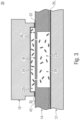
- Fig. 3 shows a schematic side view of a detector cell 30 according to an embodiment.
- the detector cell 30 may be formed similar to the detector cell 20.
- a coating layer 26 which may be the coating layer 26 of detector cell 20
- another coating layer 26 2 may be arranged at the layer structure 16 or as a part thereof, for example, so as to face the membrane structure 18.
- the coating layer 26, and the coating layer 26 2 both are optional, the configuration of detector cell 20 and of detector cell 30 allows that a part of the cavity is sealed by a reflective coating from light or electromagnetic radiation adapted to excite the target medium 34 in the cavity.
- the membrane structure 18 described in connection with detector cell 10, 20 and/or 30 may be evaluated for a vibration thereof.
- the detector cell 10, 20 and/or 30 may comprise a circuitry being configured for evaluating the vibration.
- the detector cell 10, 20 and/or 30 may be connectable to a suited circuitry, for example, using conductive structures 42.
- the membrane structure 18 may be arranged, for example, in a single-backplate configuration or a dual-backplate configuration.
- a single-backplate configuration may refer to a configuration according to which a vibration of the membrane having a conductive surface is evaluated with regard to one counter electrode arranged adjacent to the membrane.
- the vibrateable membrane may be sandwiched between two counter-electrodes.
- the layer structure 14 may comprise a single backplate configuration or a dual-backplate configuration for the membrane structure 18.
- the detector cell 10, 20 and/or 30 may comprise a piezoelectric or a piezo-resistive element so as to determine a deformation or vibration of the membrane structure 18.
- Fig. 4a shows a schematic side view of the layer structure 14 having the microphone structure 18, the seal ring 32 and conductive structure 42.
- the conductive structure 42 may be, for example, a metallization using a metal material such as gold, silver, aluminum, copper or the like.
- the membrane structure 18 may be a single backplate structure or a dual backplate structure. In the figures of the present disclosure, the membrane structure and counter electrodes are displayed as a single block so as to facilitate the understanding of embodiments.
- the layer structure 14 may be similar to a silicon based microphone structure.
- a native insulating layer, for example, SiO 2 on a substrate backside may be removed, for example, using a HF (hydrogen fluoride) dip.
- Fig. 4b shows a schematic side view of a configuration of the layer structure 12, for example, comprising the substrate layer 28 at the present stage.
- the substrate layer 28 may be, for example, at least a part of a silicon wafer but may also comprise other materials.
- the substrate layer 12 may be a wafer to be diced or separated later.
- Fig. 4c shows a schematic side view of the layer structure 12.
- the deposition of the coating layer 26 may comprise a deposition of a metal material such as gold or the like on the silicon wafer.
- the deposition of the coating layer 26 may include a deposition of an adhesion layer, for example, tin (Ti).
- Ti tin
- the coating layer 26 may serve for multiple purposes. For example, it may serve for forming an alloy with the layer structure 14 when performing a wafer level bonding (WLB). Further, it may serve as a reflection plane for optical radiation, e.g., electromagnetic radiation 54.
- Fig. 4d shows a schematic side view of a configuration of layer structures 12 of Fig. 4c and of layer structure 14 of Fig. 4a prior to a step of combining both layer structures
- Fig. 4e shows a schematic side view of layer structures 12 and 14 after the wafer level bonding.
- the interface 24 may be obtained allowing for a tight connection of layer structures 12 and 14.
- the interface 24 may comprise the alloy comprising material of the coating layer 26 and of the semiconductor material of layer structure 14, e.g., silicon material.
- the described eutectic Au/Si bond may be performed, for example, under a vacuum atmosphere or any other suitable atmosphere as the target gas may be included later when the membrane structure 18 comprises ventilation holes. Alternatively, a sealed sub-cavity may be bonded under the target atmosphere.
- Fig. 4f shows a schematic side view of layer structure 16, the layer structure 16 may comprise a topographic structure.
- an interface forming material 56 e.g., a gold material, an aluminum material, a tin material or a silver material or the like, including materials forming an alloy, e.g., gold/tin may be arranged as described for the conductive layer 26.
- Recesses 58 1 , 58 2 , and/or 58 3 may be arranged. Recess 58 2 may later provide at least partially for the sub-cavity 22b whilst recesses 58 1 and 58 3 may allow for facilitating a later dicing.
- material may be removed, e.g., based on etching or grinding, until a level indicated by a line L is reached.
- the recesses 58 1 , 58 2 and/or 58 3 may be optional.
- the sub-cavity 22b may also be formed as a recess in the layer structure 14, e.g., when arranging the membrane structure 18 in a center of the layer structure 14 with regard to the extension 44 2 illustrated in Fig. 2a .
- a Si-cap may be built with a gold-Sn solder 56 at contact position.
- the singulation of the final dies may be done by grinding. This may allow for preventing cracks in the structure.
- a silicon wafer may be used into which the recesses 58, and 58 3 may be structured, for example, using an action process.
- the recesses 58, and 58 3 may be a same recess, for example, having a rectangular, elliptic or circular course. That is, a structuring of a first cavity 58 1 , 58 3 may be performed into a silicon wafer 62.
- the recess 58 2 may be generated, for example, using an etching process. Etching may be performed as wet etching or dry etching or other concepts to remove material. That is, a structuring of a second cavity 58 2 may be performed into the silicon wafer 62.
- the interface forming material 56 may be arranged at contact positions or contact regions 64 of the wafer 62. That is, in regions where layer structures 14 and 16 are deemed to contact each other, the interface forming material 56 may be arranged at least partially. Alternatively or in addition, the interface forming material 56 may also be arranged at the layer structure 14. In other words, a deposition of AuSn is performed at contact position.
- the coating layer 26 2 may be arranged in recess 58 2 prior or afterwards or simultaneously.
- the structure illustrated in Fig. 4e and the structure illustrated in Fig. 4i may both be arranged into a processing chamber that may comprise the target medium 34. It is to be noted that the wafer level bonding being described in connection with Fig. 4e may also be performed in an atmosphere having the target medium 34. Alternatively, the wafer level bonding described in Fig. 4e may be performed under a different atmosphere when compared to the wafer level bonding of Fig. 4j . This may allow for hosting different media, pressures, or concentrations of gases in different sub-cavities being sealed from each other. One of such sealed cavities may also comprise a low pressure or vacuum, that is, the processing chamber may be evacuated when performing the wafer level bonding.
- layer structures 14 and 16 may mechanically be connected to each other. It is noted that wafer level bonding of layer structures 12 and 14 may be performed simultaneously or after having bonded layer structures 14 and 16.
- a wafer bonding of the top sealing wafer 16 may be performed on a metallization of the microphone (here: AuSn-Au bond).
- a metallization of the microphone here: AuSn-Au bond.
- Other bonding techniques i.e., other materials are possible.
- the process may be done under a target atmosphere, e.g., CO 2 . Depending on the target gas to be detected, also one or more different atmospheres may be chosen.
- the single detector cells may be separated from each other by removing a part of the layer structure 16, for example, starting from a side 16A, e.g., a top side, until the line L such that a configuration similar to Fig. 4k may be obtained.
- Layer structures 12 and/or 16 may be diced as those structures are mechanically robust.
- the final device may comprise a Si-microphone with a top and a bottom sealing wafer 12 and 16.
- a target media CO 2
- the design of the Si-cap can be adjusted, e.g., the height of the cavity.
- the overall shape of the resulting cap after singulation can be adjusted as shown, for example, in Fig. 2 , e.g., with more DRIE (deep reactive ion etching processes) during structuring before the WLB process.
- a dual backplate Si-microphone may be used, wherein also different SiMiC (silicon microphone) technology may be used.
- a bottom sealing wafer which may allow for an easy handling.
- the Si wafer may be coated with Au which may include a Ti adhesion layer.
- a HF dip may be used to remove native SiO 2 on a MEMS backside.
- An Au/Si eutectic bond may be performed, for example, using approximately 360°C.
- the top wafer may be processed by processing a Si cap wafer, which can be done on a carrier wafer.
- An AuSn/Au diffusion bond may be performed, e.g., by applying a temperature of approximately 320°C. Then, a release may be performed.
- Fig. 5 shows a schematic block diagram of a photoacoustic gas sensor according to an embodiment.
- the photoacoustic gas sensor 50 may comprise the detector cell 10, wherein alternatively or in addition one or more different detector cells may be arranged, for example, detector cell 20 and/or 30.
- the photoacoustic gas sensor may comprise an electromagnetic source 66 configured for emitting the electromagnetic radiation 54 so as to excite a movement of the membrane structure 18 based on an asymmetric energy absorption of the electromagnetic radiation in sub-cavities 22a and 22b of the cavity of the detector cell.
- the photoacoustic gas sensor 50 may comprise a control unit 68 configured for evaluating the vibration of the membrane structure 18 and/or for controlling the electromagnetic source 66. That is, the control unit 68 may be in communication with the detector cell 10 and/the electromagnetic source 66.
- the control unit 68 may comprise, for example, a processor, a microcontroller, a field programmable gate array (FPGA) and/or an application specific integrated circuit (ASIC).
- the detector cell 10, the detector cell 20 and/or the detector cell 30 may be obtained by processing on a wafer level.
- Embodiments relate to a chip-scaled packaging of a photoacoustic gas sensor, i.e., to chip-scaled packaged photoacoustic gas sensors.
- Fig. 6 shows a schematic block diagram of a chip-scaled packaged photoacoustic gas sensor 60 according to an embodiment.
- the chip-scaled packaged photoacoustic gas sensor 60 may comprise a detector cell 65.
- the detector cell 65 may have a membrane structure, e.g., the membrane structure 18 inside a detector cell cavity, e.g., cavity 22.
- Sub-cavities 22a and 22b of cavity 22 may be arranged on different sides of the membrane structure 18.
- the chip-scaled packaged photoacoustic gas sensor 60 may comprise the that the electromagnetic source or emitter 66 which may comprise a spacing 74 and a casing 76 and an emitting element E that may generate the electromagnetic radiation 54, for example, based on a heating. That is, the element E may be a heater. Alternatively, the element E may be a black body or the like.
- the electromagnetic source 66 may be configured for emitting the electromagnetic radiation 54 so as to excite a movement of the membrane structure 18 based on the described asymmetric energy absorption of the electromagnetic radiation 54 in sub-cavity 22a and sub-cavity 22b.
- the chip-scaled package photoacoustic gas sensor may be implemented such that the sub-cavities 22a and 22b have different sizes and/or different surface ratios so as to at least partially obtain the asymmetric energy absorption as described for the detector cells.
- the electromagnetic source 66 may be implemented to provide for a pulsed excitation of the electromagnetic radiation 54, e.g., based on a respective control signal.
- a frequency of the pulsing and/or a wavelength of the signal may be adapted to the target gas and/or the resonance frequency of the membrane structure.
- the electromagnetic radiation 54 may be referred to as light even if comprising harshly or completely invisible wavelengths when compared to human abilities.
- the detector cell 65 may be implemented as described for the detector cell 10, 20 and/or 30.
- a configuration may be implemented in which sub-cavities 22a and 22b are sealed from each other.
- the target medium 34 may be arranged in at least one sub-cavity 22a and/or 22b.
- the possible other sub-cavity may comprise a different target medium or no target medium, i.e., it may be evacuated.
- the asymmetric energy absorption may be based on an asymmetric energy input into the sub-cavity 22a and the sub-cavity 22b from the electromagnetic radiation 54.
- the asymmetric energy absorption may be based on an asymmetric energy loss from sub-cavity 22a and sub-cavity 22b.
- Such an energy loss may be obtained, for example, by having different sizes of wall structures surrounding the cavities and/or different thermal conductivity.
- the energy loss may thus be based on an energy input of the electromagnetic energy or electromagnetic radiation into the sub-cavities 22a and 22b.
- the energy loss may thus be related to a thermal loss path that may lead to a reduction of resulting pressure in the target medium 34, e.g., by cooling due to the energy loss.
- the chip-scaled packaged photoacoustic gas sensor 60 may comprise a substrate 72 on which the detector cell 65, the electromagnetic source 66 and/or the control unit 68 may be arranged.
- the substrate 72 may comprise a semiconductor material or a glass material or a ceramic material or a combination thereof. So as to allow for a low thermal loss, the electromagnetic source 66 may be spaced from the substrate 72 by a spacing structure 74 and/or encapsulated by a casing 76.
- the electromagnetic source 66 may form an emitter together with the casing 76.
- the emitter may include a filter for filtering a wavelength to be emitted towards the detector cell 65, for example, so as to avoid ambiguities in measurement results obtained by the control unit 68.
- the fluid in the cavity may comprise a target frequency at which the fluid is resonant.
- the chip-scaled packaged photoacoustic gas sensor may be implemented so as to comprise a filter structure, e.g., as part of the housing 76 and/or of the spacing structure 74 or arranged between the emitting element E and the detector cell 65.
- the filter structure may be arranged for filtering the electromagnetic radiation 54 so as to attenuate a wavelength not corresponding to the target frequency in a larger amount, i.e. at least 20 %, at least 30 %, at least 50 % or more, when compared to a wavelength corresponding to the target frequency.
- the filter structure is incorporated in the casing 76 or the filter structure implements the casing 76.
- the chip-scaled packaged photoacoustic gas sensor 60 may comprise a housing 78 forming an enclosure for at least the electromagnetic source 66 and the detector cell 65, wherein additional components may be arranged, for example, the control unit 68. That is, the chip-scaled package photoacoustic gas sensor 60 may comprise a lid 78 at least partially forming a cavity 86 of the chip-scaled packaged photoacoustic gas sensor. The cavity 86 may host at least the detector cell 65 and the electromagnetic source 66. The lid 78 may be reflective for the electromagnetic radiation.
- the enclosure may comprise a ventilation or opening 82 to allow environmental medium 84, e.g., air or a different medium, to travel into an interior 86 of the enclosure.
- the chip-scaled packaged photoacoustic gas sensor may comprise an inlet so as to let pass a target medium, i.e., the environmental medium 84.
- the environmental medium 84 may thus be subjected to the electromagnetic radiation and may absorb energy therefrom at least in some specific wavelength ranges.
- a content of the environmental medium 84 may be determined. That is at least a presence or concentration of the target medium 34 may be determined in the environmental medium 84.
- a gas sensor cell including the WLB detector unit is disclosed.
- An infrared emitter may be packaged within the same housing next to a detector unit with corresponding ASIC for the read-out of the detector unit.
- a distance 88 between the source 66 and side 78A may be small, for example, a preferably non-zero value of at most 1 mm, 500 ⁇ m or 100 ⁇ m. Such a small distance 88 may allow the electromagnetic radiation 54 to essentially arrive at the detector cell from a lateral side to excite the target medium 34. This may allow for a same or comparable energy input into the sub-cavities 22a and 22b.
- a shielding 92 may be arranged between the electromagnetic source 66 and the detector cell 65.
- the shielding 92 may be configured for partially shielding the detector cell 65 from the electromagnetic radiation 54 so as to at least partially obtain the asymmetric energy absorption.
- the shielding 92 may at least partially shield sub-cavity 22a and/or at least partially shield sub-cavity 22b. For example, only one of both sub-cavities is shielded or the sub-cavities are shielded by a different extent.
- Fig. 7 shows a schematic side view of a chip-scaled packaged photoacoustic gas sensor according to an embodiment.
- the distance 88 may be larger when compared to the chip-scaled packaged photoacoustic gas sensor 60, for example, having a distance larger than described in connection with Fig. 6 .
- An example value that does not limit the described embodiments may be between 0.5 mm and 5 mm, between 0.75 mm and 3 mm or between 1 mm and 2.5 mm such as 1.6 mm.
- the distance 88 may be measured between a main side 78A which is spaced from the emitter and the detector cell 65 by a circumferential side 78B of the lid 78.
- the large distance 88 may allow scattering of the electromagnetic radiation 54 towards the detector cell 65 at the main side 78A.
- the small distance shown in Fig. 6 may prevent scattering of the electromagnetic radiation 54 towards the detector cell 65 at the main side 78A such that the electromagnetic radiation 54 laterally travels towards the detector cell 65.
- a gas sensor unit may include the WLB detector unit.
- An infrared emitter may be packaged within the same housing next to the detector unit with corresponding ASIC for the read-out of the detector unit.
- the distance from the detector top side to the lid of the sensor unit may be big enough in order to have optical access to the top side of the detector unit.
- the light may be scattered and reflected within the main optical shielding (module package) making it hard to determine a main angle of incidence.
- the control unit 68 i.e. the circuit, may be covered with a material 94 being intransparent for the electromagnetic radiation 54. Such an arrangement is optional. Alternatively or in addition but also optionally, the control unit or circuit 68 may be insensitive for the electromagnetic radiation 54 such that in both cases, the electromagnetic radiation 54 does not harm an operation of the control unit 68.
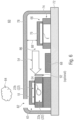
- Fig. 8 shows a schematic side view of a chip-scaled packaged photoacoustic gas sensor 80 according to an embodiment.
- the lid 78 may be formed as described in connection with the chip-scaled packaged photoacoustic gas sensor 70 but may also be formed as described for the chip-scaled photoacoustic gas sensor 60.
- a detector cell 85 of the chip-scaled photoacoustic gas sensor 85 comprises a reflective coating 26 2 completely or at least to an amount of more than 50 %, more than 70 % or more than 90 % covering or shielding one of the sub-cavities 22a or 22b, e.g. sub-cavity 22b.
- Such a reflective coating 26 2 may be applied, for example, to an electrode 96 of the single backplate configuration or dual-backplate configuration of the microphone chip to prevent the light from shining through the bottom interface of the top volume, i.e. to prevent the electromagnetic radiation 54 to travel through the sub-cavity 22b to the sub-cavity 22a.
- the WLB may include a reflective coating of the inner or outer surfaces of the top sealing cap wafer, i.e. layer structure 16.
- layer structure 16 i.e. direct optical access into the upper gas volume 22b can be avoided.
- Fig. 9 shows a schematic side of a chip-scaled packaged photoacoustic gas sensor 90 according to an embodiment.
- the chip-scaled packaged photoacoustic gas sensor 90 may comprise a stacked configuration.
- Different sub-packages 98, and 98 2 may be stacked with regard to each other and may thus extend to a different perpendicular extension when compared to the chip-scaled packaged photoacoustic gas sensors 60, 70 and 80. Whilst reducing a required surface with the stacked arrangement, a height may be increased.
- Sub-package 98 1 may comprise the electromagnetic source 66, for example including a filter.
- sub-package 98 2 may be spaced with a spacing structure or spacer or thermally decoupling element 102 being arranged between a substrate 72, and a substrate 72 2 of the sub-packages 98, and 98 2 .
- the thermally decoupling element 102 may comprise a low thermal conductance.
- a polymer material or the like may be used.
- Sub-package 98 2 may comprise the detector cell 65.
- the control unit 68 may be arranged in sub-package 98, or 98 2 .
- the electromagnetic radiation 54 may travel from the sub-package 98, to the sub-package 98 2 .
- substrate 72 2 may comprise an opening 104 or an area of low thermal conductance.
- embodiments relate to a closed photoacoustic gas sensing cell comprising an infrared emitter, an optical filter and a detector unit (e.g., a Si-microphone) enclosed by a housing (package).
- the detector unit (microphone) may be enclosed in a hermetically sealed package under a defined atmosphere of the gas of interest (e.g., a specific percentage CO 2 , a target gas in a target concentration).
- the package of the detector unit may be hermetically sealed over lifetime, e.g., at least 5 years and possible ranging to 15 years. This requirement may be addressed with embodiments described herein that provide for a packaging process and corresponding structures.
- a wafer level bonding (WLB) processes under a desired atmosphere may decrease the packaging cost per unit since the whole packaging process may be performed on all devices still on wafer level. That is, may be prevented to fill single devices individually.
- WLB processes may furthermore decrease the form factor of the gas sensing detector unit in comparison to a standard packaging method and therefore enables further possibilities for integration into small-scale PCBs (printed circuit board), e.g. mobile phone applications.
- a hermetically sealed gas detector unit can be formed by wafer level processes, thereby the unit may comprise a microphone wafer, a top sealing wafer acting as a cap above the membrane area as well as a bottom sealing wafer.
- the bottom and top sealing wafer can be equipped with reflective coating for optical shielding of the upper (above the microphone membrane) or lower (below the microphone membrane) gas volume from the outside.
- a very small enclosed gas volume can be realized, depending only or at least essentially on the thickness of the microphone wafer and the cavity in the top sealing wafer above the microphone front side. Values stated for single thicknesses do not limit the process limitations.
- Pulsed excitation with an infrared light source may lead to a pressure difference between above and below the microphone membrane within the enclosed gas volume and may thus lead to an acoustic signal dependent on the intensity of the infrared light.
- the ASIC may be covered with light non-transparent material, e.g., globe top, or may be robust against broadband light.
- a gas exchange may be provided through openings in the optical shielding, depending on the optical path the ventilation can be adjusted in order to enhance the gas exchange diffusion time. With more light absorbed through the optical path outside of the detector unit (higher ambient CO 2 concentration), the photoacoustic pressure within the detector cell may get smaller, i.e., an inverse signal may be obtained at the ASIC.
- the WLB photoacoustic detector unit can be included in a photoacoustic sensor comprising, for example, a chopped MEMS infrared emitter, electromagnetic source, an optical filter for wavelength selective heating of a gas, the hermetically sealed MEMS microphone using WLB processes and a housing.
- the system may be operated by an internal ASIC which provides the input power of the infrared emitter as well as the acoustical read-out of the WLB detector unit.
- Embodiments are based on produced hermetically sealed MEMS microphones under a dedicated gas atmosphere using wafer level bonding processes.
- the small hermetically enclosed gas volume may be beneficial for creating a photoacoustic pressure. It is mentioned that the ration between the two volumes (above and below the microphone membrane, the sub-cavities) may be important for the response of the detector unit to chopped infrared light. Optical shielding of one of the volumes (e.g. by metal coating of the inner part of the top volume) may enhance the detector sensitivity.
- the height of the WLB PAS (photoacoustic sensor) detector cell may be defined or at least influenced by the thickness of the three wafers (layer structures) as well as the height of the cavity above the MEMS microphone. Thus, this may form a chip-sized solution to design a hermetically sealed WLB PAS detector cell with a height range which is possibly exclusively defined by process windows for the respective three wafers. This may allow to provide small WLB PAS detector cells.
- Detector cells may be a stand-alone product but may also be included into photoacoustic gas sensors. This may provide for advantages compared to NDIR (non-dispersive infrared sensor) detectors.
- Embodiments relate to an infrared source that is integrated into the WLB process of the detector unit, e.g. as top or bottom wafer.
- the optical filter wafer may be used as top or bottom sealing wafer. That is, a process for manufacturing the electromagnetic source 66 may be similar to producing a MEMS microphone.
- the structure 74 and/or 76 may thus include filtering properties.
- aspects have been described in the context of an apparatus, it is clear that these aspects also represent a description of the corresponding method, where a block or device corresponds to a method step or a feature of a method step. Analogously, aspects described in the context of a method step also represent a description of a corresponding block or item or feature of a corresponding apparatus.
Landscapes
- Chemical & Material Sciences (AREA)
- Health & Medical Sciences (AREA)
- Life Sciences & Earth Sciences (AREA)
- Physics & Mathematics (AREA)
- Immunology (AREA)
- Biochemistry (AREA)
- General Health & Medical Sciences (AREA)
- General Physics & Mathematics (AREA)
- Analytical Chemistry (AREA)
- Pathology (AREA)
- Engineering & Computer Science (AREA)
- Combustion & Propulsion (AREA)
- Food Science & Technology (AREA)
- Medicinal Chemistry (AREA)
- Optics & Photonics (AREA)
- Investigating Or Analysing Materials By Optical Means (AREA)
- Micromachines (AREA)
- Photometry And Measurement Of Optical Pulse Characteristics (AREA)
Claims (18)
- Detektorzelle für einen photoakustischen Gassensor, die folgende Merkmale aufweist:eine erste Schichtstruktur (12);eine zweite Schichtstruktur (14), die an der ersten Schichtstruktur angeordnet ist und eine Membranstruktur (18) aufweist; undeine dritte Schichtstruktur (16), die an der zweiten Schichtstruktur (14) angeordnet ist;wobei die erste Schichtstruktur (12) und die dritte Schichtstruktur (16) einen Hohlraum (22) hermetisch umschließen und wobei die Membranstruktur (18) in dem Hohlraum angeordnet ist;dadurch gekennzeichnet, dasseine für elektromagnetische Strahlung (54) reflektierende Beschichtungsschicht (26) an einer Oberfläche der ersten Schichtstruktur (12), die der Membranstruktur (18) zugewandt ist, oder an einer Oberfläche der dritten Schichtstruktur (16), die der Membranstruktur (18) zugewandt ist, angeordnet ist.
- Detektorzelle gemäß Anspruch 1, bei der die zweite Schichtstruktur (16) zumindest einen Teil einer Seitenwand (10A) der Detektorzelle bildet.
- Detektorzelle gemäß Anspruch 1 oder 2, bei der die zweite Schichtstruktur (14) für eine elektromagnetische Strahlung (54) durchlässig ist.
- Detektorzelle gemäß einem der vorhergehenden Ansprüche, bei der der Hohlraum (22) akustisch isoliert ist; wobei die Membran (18) mit Bezug auf akustischen Schall an einem Außenbereich des Hohlraums (22) nur zu einem vernachlässigbaren Effekt schwingungsfähig ist oder für akustischen Schall unempfindlich ist.
- Detektorzelle gemäß einem der vorhergehenden Ansprüche, bei der die erste Schichtstruktur (12) und die zweite Schichtstruktur (14) durch Waferebenenbonden aneinander angebracht sind und/oder wobei die zweite Schichtstruktur (14) und die dritte Schichtstruktur (16) durch Waferebenenbonden aneinander angebracht sind.
- Detektorzelle gemäß einem der vorhergehenden Ansprüche, die in Bezug auf eine Empfindlichkeit gegenüber elektromagnetischer Strahlung (54) eines ersten Unterhohlraums (22a) des Hohlraums (22) zwischen der ersten Schichtstruktur (12) und der zweiten Schichtstruktur (14) und eines zweiten Unterhohlraums (22b) zwischen der zweiten Schichtstruktur (14) und der dritten Schichtstruktur (16) asymmetrisch ist.
- Detektorzelle gemäß einem der vorhergehenden Ansprüche, bei der die Beschichtungsschicht (26) zumindest ein reflektierendes Material oder eine reflektierende Struktur aufweist.
- Detektorzelle gemäß einem der vorhergehenden Ansprüche, die eine Grenzfläche (24) mit der zweiten Schichtstruktur (14) aufweist, die ein Ergebnis eines Waferbondingprozesses unter Verwendung eines Materials der Beschichtungsschicht (26) ist.
- Detektorzelle gemäß einem der vorhergehenden Ansprüche, bei der eine erste Erweiterung (521) eines ersten Unterhohlraums (22a) zwischen der ersten Schichtstruktur (12) und der zweiten Schichtstruktur (14) und eine zweite Erweiterung (522) eines zweiten Unterhohlraums (22b) zwischen der zweiten Schichtstruktur (14) und der dritten Schichtstruktur (16) entlang einer Richtung (46), die parallel zu einer Oberflächennormalen (N2) einer Hauptseite der Membranstruktur (18) ist, unterschiedlich sind.
- Detektorzelle gemäß einem der vorhergehenden Ansprüche, die ein Zielmedium (34) zwischen der ersten und der dritten Schichtstruktur aufweist.
- Detektorzelle gemäß einem der vorhergehenden Ansprüche, bei der zumindest die erste Schichtstruktur (12), die zweite Schichtstruktur (14) oder die dritte Schichtstruktur (16) für ein mittelwelliges Infrarotspektrum durchlässig ist.
- Detektorzelle gemäß einem der vorhergehenden Ansprüche, bei der zum Messen einer Bewegung der Membranstruktur (18)
die Detektorzelle ein piezoelektrisches Element oder ein piezoresistives Element aufweist. - Detektorzelle gemäß einem der vorhergehenden Ansprüche, bei der die Membranstruktur zumindest ein Lüftungsloch (36) aufweist.
- Detektorzelle gemäß einem der Ansprüche 1 bis 12, bei der ein erster Unterhohlraum (22a) des Hohlraums (22) an einer ersten Seite der Membranstruktur (18) und ein zweiter Unterhohlraum (22b) des Hohlraums (22) an einer zweiten Seite der Membranstruktur (18) voneinander abgedichtet sind und unterschiedliche Gase oder Gaskonzentrationen aufweisen.
- Detektorzelle gemäß einem der vorhergehenden Ansprüche, bei der ein Teil des Hohlraums (22) durch eine reflektierende Beschichtung gegen Licht abgedichtet ist, das angepasst ist, um ein Fluid in dem Hohlraum (22) anzuregen.
- Ein photoakustischer Gassensor, der folgende Merkmale aufweist:eine Detektorzelle (10; 20; 30) gemäß einem der vorhergehenden Ansprüche; undeine elektromagnetische Quelle (66), die zum Emittieren einer elektromagnetischen Strahlung (54) konfiguriert ist, um eine Bewegung der Membranstruktur (18) basierend auf einer asymmetrischen Energieabsorption der elektromagnetischen Strahlung (54) in verschiedenen Unterhohlräumen (22a-b) des Hohlraums (22), die auf verschiedenen Seiten der Membranstruktur (18) angeordnet sind, anzuregen.
- Verfahren zum Herstellen einer Detektorzelle, wobei das Verfahren folgende Schritte aufweist:Bereitstellen einer ersten Schichtstruktur (12);Anbringen einer zweiten Schichtstruktur (14), die eine Membranstruktur (18) aufweist, an der ersten Schichtstruktur (12); undAnbringen einer dritten Schichtstruktur (16) an der zweiten Schichtstruktur (14);derart, dass die erste Schichtstruktur (12) und die dritte Schichtstruktur (16) einen Hohlraum (22) hermetisch umschließen und derart, dass die Membranstruktur (18) in dem Hohlraum angeordnet ist;dadurch gekennzeichnet, dass das Verfahren ferner folgende Schritte aufweist:
Anordnen einer Beschichtungsschicht (26), die elektromagnetische Strahlung (54) reflektiert, an einer Oberfläche der ersten Schichtstruktur (12), die der Membranstruktur (18) zugewandt ist, oder an einer Oberfläche der dritten Schichtstruktur (16), die der Membranstruktur (18) zugewandt ist. - Verfahren gemäß Anspruch 17, bei dem das Anbringen der zweiten Schichtstruktur (14) an der ersten Schichtstruktur (12) und/oder das Anbringen der dritten Schichtstruktur (16) an der zweiten Schichtstruktur (14) ein Waferebenenbonden aufweist.
Priority Applications (6)
| Application Number | Priority Date | Filing Date | Title |
|---|---|---|---|
| EP23153185.6A EP4191232A1 (de) | 2019-08-22 | 2019-08-22 | Detektorzelle für einen photoakustischen gassensor und photoakustischer gassensor |
| EP19193158.3A EP3783339B1 (de) | 2019-08-22 | 2019-08-22 | Detektorzelle für einen photo-akustischen gassensor sowie photo-akustischer gassensor |
| US16/935,726 US11346767B2 (en) | 2019-08-22 | 2020-07-22 | Detector cell for a photoacoustic gas sensor and photoacoustic gas sensor |
| KR1020200100537A KR102416266B1 (ko) | 2019-08-22 | 2020-08-11 | 광음향 가스 센서를 위한 검출기 셀 및 광음향 가스 센서 |
| CN202010836799.3A CN112414947B (zh) | 2019-08-22 | 2020-08-19 | 用于光声气体传感器的检测器单元和光声气体传感器 |
| US17/658,544 US12000772B2 (en) | 2019-08-22 | 2022-04-08 | Detector cell for a photoacoustic gas sensor and photoacoustic gas sensor |
Applications Claiming Priority (1)
| Application Number | Priority Date | Filing Date | Title |
|---|---|---|---|
| EP19193158.3A EP3783339B1 (de) | 2019-08-22 | 2019-08-22 | Detektorzelle für einen photo-akustischen gassensor sowie photo-akustischer gassensor |
Related Child Applications (2)
| Application Number | Title | Priority Date | Filing Date |
|---|---|---|---|
| EP23153185.6A Division-Into EP4191232A1 (de) | 2019-08-22 | 2019-08-22 | Detektorzelle für einen photoakustischen gassensor und photoakustischer gassensor |
| EP23153185.6A Division EP4191232A1 (de) | 2019-08-22 | 2019-08-22 | Detektorzelle für einen photoakustischen gassensor und photoakustischer gassensor |
Publications (2)
| Publication Number | Publication Date |
|---|---|
| EP3783339A1 EP3783339A1 (de) | 2021-02-24 |
| EP3783339B1 true EP3783339B1 (de) | 2023-04-19 |
Family
ID=67810360
Family Applications (2)
| Application Number | Title | Priority Date | Filing Date |
|---|---|---|---|
| EP19193158.3A Active EP3783339B1 (de) | 2019-08-22 | 2019-08-22 | Detektorzelle für einen photo-akustischen gassensor sowie photo-akustischer gassensor |
| EP23153185.6A Pending EP4191232A1 (de) | 2019-08-22 | 2019-08-22 | Detektorzelle für einen photoakustischen gassensor und photoakustischer gassensor |
Family Applications After (1)
| Application Number | Title | Priority Date | Filing Date |
|---|---|---|---|
| EP23153185.6A Pending EP4191232A1 (de) | 2019-08-22 | 2019-08-22 | Detektorzelle für einen photoakustischen gassensor und photoakustischer gassensor |
Country Status (4)
| Country | Link |
|---|---|
| US (2) | US11346767B2 (de) |
| EP (2) | EP3783339B1 (de) |
| KR (1) | KR102416266B1 (de) |
| CN (1) | CN112414947B (de) |
Families Citing this family (11)
| Publication number | Priority date | Publication date | Assignee | Title |
|---|---|---|---|---|
| FR3104259B1 (fr) * | 2019-12-06 | 2024-03-01 | Commissariat Energie Atomique | Dispositif pour la caractérisation photo-acoustique d’une substance gazeuse et procédé de fabrication d’un tel dispositif |
| DE102019134279B3 (de) | 2019-12-13 | 2021-05-27 | Infineon Technologies Ag | Photoakustische Sensoren und MEMS-Bauelemente |
| EP3863371A1 (de) * | 2020-02-07 | 2021-08-11 | Infineon Technologies AG | Ir-strahler mit glasdeckel |
| US12597658B2 (en) | 2021-02-23 | 2026-04-07 | Lg Energy Solution, Ltd. | Secondary battery, battery pack, and automobile |
| KR20230169106A (ko) | 2021-03-04 | 2023-12-15 | 한-식카드-게셀쉐프트 퓨어 안게반테 포슝 이.브이. | Mems 셀에 기준 가스를 포집하는 방법 |
| CN113624718B (zh) * | 2021-08-13 | 2023-08-18 | 哈尔滨工业大学 | 基于压阻薄膜的光声光谱痕量气体检测装置及方法 |
| US12092566B2 (en) * | 2022-04-19 | 2024-09-17 | Honeywell International Inc. | Encapsulating of photoacoustic detector |
| CN116046710A (zh) * | 2022-12-30 | 2023-05-02 | 广州奥松电子股份有限公司 | 光学气体传感器及制造方法 |
| CN116183513A (zh) * | 2023-02-28 | 2023-05-30 | 西安交通大学 | 一种芯片级集成的光声光谱气体传感器 |
| WO2024213315A1 (en) * | 2023-04-14 | 2024-10-17 | Ams-Osram Ag | Compact gas sensor using self-mixing interferometry in the laser cavity, the laser cavity being directly attached to the gas chamber |
| EP4530606A1 (de) * | 2023-09-26 | 2025-04-02 | Infineon Technologies AG | Halbleiterbauelemente, gassensor mit mikroelektromechanischem system, verfahren |
Citations (2)
| Publication number | Priority date | Publication date | Assignee | Title |
|---|---|---|---|---|
| WO2017207399A1 (de) * | 2016-06-03 | 2017-12-07 | Robert Bosch Gmbh | Mikroelektronische sensorvorrichtung und verfahren zum herstellen einer mikroelektronischen sensorvorrichtung |
| US20190208330A1 (en) * | 2017-12-29 | 2019-07-04 | Infineon Technologies Ag | Mems component and mobile device comprising the mems component |
Family Cites Families (9)
| Publication number | Priority date | Publication date | Assignee | Title |
|---|---|---|---|---|
| CA2323675A1 (en) * | 1999-10-21 | 2001-04-21 | Vincent Y. Chow | Closed cell gas detector |
| JP5043556B2 (ja) * | 2007-08-09 | 2012-10-10 | セイコーNpc株式会社 | 水素ガスセンサ |
| KR20090064693A (ko) * | 2007-12-17 | 2009-06-22 | 한국전자통신연구원 | 마이크로 가스 센서 및 그 제작 방법 |
| US9513261B2 (en) * | 2013-10-14 | 2016-12-06 | Infineon Technologies Ag | Photoacoustic gas sensor device and a method for analyzing gas |
| DE202015002315U1 (de) * | 2015-03-27 | 2015-05-06 | Infineon Technologies Ag | Gassensor |
| DE102015106373B4 (de) * | 2015-04-24 | 2023-03-02 | Infineon Technologies Ag | Photoakustisches gassensormodul mit lichtemittereinheit und einer detektoreinheit |
| DE102016216875A1 (de) * | 2015-09-07 | 2017-03-09 | Infineon Technologies Ag | Vorrichtung und Verfahren für eine In-situ-Kalibrierung eines photoakustischen Sensors |
| US10347814B2 (en) * | 2016-04-01 | 2019-07-09 | Infineon Technologies Ag | MEMS heater or emitter structure for fast heating and cooling cycles |
| FR3078155B1 (fr) * | 2018-02-19 | 2020-08-14 | Commissariat Energie Atomique | Capteur photo-acoustique avec couplage opto-mecanique. |
-
2019
- 2019-08-22 EP EP19193158.3A patent/EP3783339B1/de active Active
- 2019-08-22 EP EP23153185.6A patent/EP4191232A1/de active Pending
-
2020
- 2020-07-22 US US16/935,726 patent/US11346767B2/en active Active
- 2020-08-11 KR KR1020200100537A patent/KR102416266B1/ko active Active
- 2020-08-19 CN CN202010836799.3A patent/CN112414947B/zh active Active
-
2022
- 2022-04-08 US US17/658,544 patent/US12000772B2/en active Active
Patent Citations (2)
| Publication number | Priority date | Publication date | Assignee | Title |
|---|---|---|---|---|
| WO2017207399A1 (de) * | 2016-06-03 | 2017-12-07 | Robert Bosch Gmbh | Mikroelektronische sensorvorrichtung und verfahren zum herstellen einer mikroelektronischen sensorvorrichtung |
| US20190208330A1 (en) * | 2017-12-29 | 2019-07-04 | Infineon Technologies Ag | Mems component and mobile device comprising the mems component |
Also Published As
| Publication number | Publication date |
|---|---|
| US12000772B2 (en) | 2024-06-04 |
| KR20210024422A (ko) | 2021-03-05 |
| CN112414947A (zh) | 2021-02-26 |
| US20210055207A1 (en) | 2021-02-25 |
| US11346767B2 (en) | 2022-05-31 |
| US20220228974A1 (en) | 2022-07-21 |
| EP3783339A1 (de) | 2021-02-24 |
| CN112414947B (zh) | 2025-07-18 |
| EP4191232A1 (de) | 2023-06-07 |
| KR102416266B1 (ko) | 2022-07-05 |
Similar Documents
| Publication | Publication Date | Title |
|---|---|---|
| US12000772B2 (en) | Detector cell for a photoacoustic gas sensor and photoacoustic gas sensor | |
| CN110836855B (zh) | 用于光声气体传感器的检测器模块 | |
| US11530980B2 (en) | Wafer arrangement for gas sensor | |
| US10451543B2 (en) | Integrated photo-acoustic gas sensor module | |
| US12078615B2 (en) | Photoacoustic detector unit, photoacoustic sensor and associated production methods | |
| CN113252569B (zh) | 具有玻璃盖的红外发射器 | |
| KR20210074201A (ko) | 광음향 센서를 위한 방출기 패키지 | |
| KR20230152135A (ko) | 광음향 가스 센서 디바이스 | |
| CN111517271B (zh) | 包括面板键合操作的方法和包括空腔的电子器件 | |
| CN115200780B (zh) | 芯片级微粒子真空腔室及其制备方法 | |
| CN112649386B (zh) | 气体传感器设备及制造该气体传感器设备的方法 | |
| EP2172755A1 (de) | Infrarotsensor mit Bandpassfilter auf der Vorderseite und evakuiertem Hohlraum | |
| JP2010243365A (ja) | 赤外線センサ装置の製造方法 | |
| KR20230095814A (ko) | 방사선 소스 디바이스 | |
| JP2013254916A (ja) | 電子部品およびその製造方法 | |
| KR20060127447A (ko) | 광학형 가스 검출 센서에 사용되는 반도체 가스셀 제조 방법 및 그 방법에 따라 제조된 반도체 가스셀 |
Legal Events
| Date | Code | Title | Description |
|---|---|---|---|
| STAA | Information on the status of an ep patent application or granted ep patent |
Free format text: STATUS: EXAMINATION IS IN PROGRESS |
|
| PUAI | Public reference made under article 153(3) epc to a published international application that has entered the european phase |
Free format text: ORIGINAL CODE: 0009012 |
|
| 17P | Request for examination filed |
Effective date: 20200625 |
|
| AK | Designated contracting states |
Kind code of ref document: A1 Designated state(s): AL AT BE BG CH CY CZ DE DK EE ES FI FR GB GR HR HU IE IS IT LI LT LU LV MC MK MT NL NO PL PT RO RS SE SI SK SM TR |
|
| AX | Request for extension of the european patent |
Extension state: BA ME |
|
| REG | Reference to a national code |
Ref country code: DE Ref legal event code: R079 Free format text: PREVIOUS MAIN CLASS: G01N0021370000 Ipc: G01N0021170000 Ref document number: 602019027652 Country of ref document: DE |
|
| GRAP | Despatch of communication of intention to grant a patent |
Free format text: ORIGINAL CODE: EPIDOSNIGR1 |
|
| STAA | Information on the status of an ep patent application or granted ep patent |
Free format text: STATUS: GRANT OF PATENT IS INTENDED |
|
| RIC1 | Information provided on ipc code assigned before grant |
Ipc: G01N 29/24 20060101ALI20220909BHEP Ipc: G01N 21/17 20060101AFI20220909BHEP |
|
| INTG | Intention to grant announced |
Effective date: 20221007 |
|
| GRAJ | Information related to disapproval of communication of intention to grant by the applicant or resumption of examination proceedings by the epo deleted |
Free format text: ORIGINAL CODE: EPIDOSDIGR1 |
|
| STAA | Information on the status of an ep patent application or granted ep patent |
Free format text: STATUS: EXAMINATION IS IN PROGRESS |
|
| GRAP | Despatch of communication of intention to grant a patent |
Free format text: ORIGINAL CODE: EPIDOSNIGR1 |
|
| STAA | Information on the status of an ep patent application or granted ep patent |
Free format text: STATUS: GRANT OF PATENT IS INTENDED |
|
| GRAS | Grant fee paid |
Free format text: ORIGINAL CODE: EPIDOSNIGR3 |
|
| INTC | Intention to grant announced (deleted) | ||
| GRAA | (expected) grant |
Free format text: ORIGINAL CODE: 0009210 |
|
| STAA | Information on the status of an ep patent application or granted ep patent |
Free format text: STATUS: THE PATENT HAS BEEN GRANTED |
|
| INTG | Intention to grant announced |
Effective date: 20230224 |
|
| AK | Designated contracting states |
Kind code of ref document: B1 Designated state(s): AL AT BE BG CH CY CZ DE DK EE ES FI FR GB GR HR HU IE IS IT LI LT LU LV MC MK MT NL NO PL PT RO RS SE SI SK SM TR |
|
| REG | Reference to a national code |
Ref country code: GB Ref legal event code: FG4D |
|
| REG | Reference to a national code |
Ref country code: DE Ref legal event code: R096 Ref document number: 602019027652 Country of ref document: DE |
|
| REG | Reference to a national code |
Ref country code: CH Ref legal event code: EP |
|
| REG | Reference to a national code |
Ref country code: IE Ref legal event code: FG4D |
|
| REG | Reference to a national code |
Ref country code: AT Ref legal event code: REF Ref document number: 1561550 Country of ref document: AT Kind code of ref document: T Effective date: 20230515 |
|
| REG | Reference to a national code |
Ref country code: LT Ref legal event code: MG9D |
|
| REG | Reference to a national code |
Ref country code: NL Ref legal event code: MP Effective date: 20230419 |
|
| P01 | Opt-out of the competence of the unified patent court (upc) registered |
Effective date: 20230804 |
|
| REG | Reference to a national code |
Ref country code: AT Ref legal event code: MK05 Ref document number: 1561550 Country of ref document: AT Kind code of ref document: T Effective date: 20230419 |
|
| PG25 | Lapsed in a contracting state [announced via postgrant information from national office to epo] |
Ref country code: NL Free format text: LAPSE BECAUSE OF FAILURE TO SUBMIT A TRANSLATION OF THE DESCRIPTION OR TO PAY THE FEE WITHIN THE PRESCRIBED TIME-LIMIT Effective date: 20230419 |
|
| PG25 | Lapsed in a contracting state [announced via postgrant information from national office to epo] |
Ref country code: SE Free format text: LAPSE BECAUSE OF FAILURE TO SUBMIT A TRANSLATION OF THE DESCRIPTION OR TO PAY THE FEE WITHIN THE PRESCRIBED TIME-LIMIT Effective date: 20230419 Ref country code: PT Free format text: LAPSE BECAUSE OF FAILURE TO SUBMIT A TRANSLATION OF THE DESCRIPTION OR TO PAY THE FEE WITHIN THE PRESCRIBED TIME-LIMIT Effective date: 20230821 Ref country code: NO Free format text: LAPSE BECAUSE OF FAILURE TO SUBMIT A TRANSLATION OF THE DESCRIPTION OR TO PAY THE FEE WITHIN THE PRESCRIBED TIME-LIMIT Effective date: 20230719 Ref country code: ES Free format text: LAPSE BECAUSE OF FAILURE TO SUBMIT A TRANSLATION OF THE DESCRIPTION OR TO PAY THE FEE WITHIN THE PRESCRIBED TIME-LIMIT Effective date: 20230419 Ref country code: AT Free format text: LAPSE BECAUSE OF FAILURE TO SUBMIT A TRANSLATION OF THE DESCRIPTION OR TO PAY THE FEE WITHIN THE PRESCRIBED TIME-LIMIT Effective date: 20230419 |
|
| PG25 | Lapsed in a contracting state [announced via postgrant information from national office to epo] |
Ref country code: RS Free format text: LAPSE BECAUSE OF FAILURE TO SUBMIT A TRANSLATION OF THE DESCRIPTION OR TO PAY THE FEE WITHIN THE PRESCRIBED TIME-LIMIT Effective date: 20230419 Ref country code: PL Free format text: LAPSE BECAUSE OF FAILURE TO SUBMIT A TRANSLATION OF THE DESCRIPTION OR TO PAY THE FEE WITHIN THE PRESCRIBED TIME-LIMIT Effective date: 20230419 Ref country code: LV Free format text: LAPSE BECAUSE OF FAILURE TO SUBMIT A TRANSLATION OF THE DESCRIPTION OR TO PAY THE FEE WITHIN THE PRESCRIBED TIME-LIMIT Effective date: 20230419 Ref country code: LT Free format text: LAPSE BECAUSE OF FAILURE TO SUBMIT A TRANSLATION OF THE DESCRIPTION OR TO PAY THE FEE WITHIN THE PRESCRIBED TIME-LIMIT Effective date: 20230419 Ref country code: IS Free format text: LAPSE BECAUSE OF FAILURE TO SUBMIT A TRANSLATION OF THE DESCRIPTION OR TO PAY THE FEE WITHIN THE PRESCRIBED TIME-LIMIT Effective date: 20230819 Ref country code: HR Free format text: LAPSE BECAUSE OF FAILURE TO SUBMIT A TRANSLATION OF THE DESCRIPTION OR TO PAY THE FEE WITHIN THE PRESCRIBED TIME-LIMIT Effective date: 20230419 Ref country code: GR Free format text: LAPSE BECAUSE OF FAILURE TO SUBMIT A TRANSLATION OF THE DESCRIPTION OR TO PAY THE FEE WITHIN THE PRESCRIBED TIME-LIMIT Effective date: 20230720 Ref country code: AL Free format text: LAPSE BECAUSE OF FAILURE TO SUBMIT A TRANSLATION OF THE DESCRIPTION OR TO PAY THE FEE WITHIN THE PRESCRIBED TIME-LIMIT Effective date: 20230419 |
|
| PG25 | Lapsed in a contracting state [announced via postgrant information from national office to epo] |
Ref country code: FI Free format text: LAPSE BECAUSE OF FAILURE TO SUBMIT A TRANSLATION OF THE DESCRIPTION OR TO PAY THE FEE WITHIN THE PRESCRIBED TIME-LIMIT Effective date: 20230419 |
|
| PG25 | Lapsed in a contracting state [announced via postgrant information from national office to epo] |
Ref country code: SK Free format text: LAPSE BECAUSE OF FAILURE TO SUBMIT A TRANSLATION OF THE DESCRIPTION OR TO PAY THE FEE WITHIN THE PRESCRIBED TIME-LIMIT Effective date: 20230419 |
|
| REG | Reference to a national code |
Ref country code: DE Ref legal event code: R097 Ref document number: 602019027652 Country of ref document: DE |
|
| PG25 | Lapsed in a contracting state [announced via postgrant information from national office to epo] |
Ref country code: SM Free format text: LAPSE BECAUSE OF FAILURE TO SUBMIT A TRANSLATION OF THE DESCRIPTION OR TO PAY THE FEE WITHIN THE PRESCRIBED TIME-LIMIT Effective date: 20230419 Ref country code: SK Free format text: LAPSE BECAUSE OF FAILURE TO SUBMIT A TRANSLATION OF THE DESCRIPTION OR TO PAY THE FEE WITHIN THE PRESCRIBED TIME-LIMIT Effective date: 20230419 Ref country code: RO Free format text: LAPSE BECAUSE OF FAILURE TO SUBMIT A TRANSLATION OF THE DESCRIPTION OR TO PAY THE FEE WITHIN THE PRESCRIBED TIME-LIMIT Effective date: 20230419 Ref country code: EE Free format text: LAPSE BECAUSE OF FAILURE TO SUBMIT A TRANSLATION OF THE DESCRIPTION OR TO PAY THE FEE WITHIN THE PRESCRIBED TIME-LIMIT Effective date: 20230419 Ref country code: DK Free format text: LAPSE BECAUSE OF FAILURE TO SUBMIT A TRANSLATION OF THE DESCRIPTION OR TO PAY THE FEE WITHIN THE PRESCRIBED TIME-LIMIT Effective date: 20230419 Ref country code: CZ Free format text: LAPSE BECAUSE OF FAILURE TO SUBMIT A TRANSLATION OF THE DESCRIPTION OR TO PAY THE FEE WITHIN THE PRESCRIBED TIME-LIMIT Effective date: 20230419 |
|
| PLBE | No opposition filed within time limit |
Free format text: ORIGINAL CODE: 0009261 |
|
| STAA | Information on the status of an ep patent application or granted ep patent |
Free format text: STATUS: NO OPPOSITION FILED WITHIN TIME LIMIT |
|
| PG25 | Lapsed in a contracting state [announced via postgrant information from national office to epo] |
Ref country code: MC Free format text: LAPSE BECAUSE OF FAILURE TO SUBMIT A TRANSLATION OF THE DESCRIPTION OR TO PAY THE FEE WITHIN THE PRESCRIBED TIME-LIMIT Effective date: 20230419 |
|
| 26N | No opposition filed |
Effective date: 20240122 |
|
| PG25 | Lapsed in a contracting state [announced via postgrant information from national office to epo] |
Ref country code: MC Free format text: LAPSE BECAUSE OF FAILURE TO SUBMIT A TRANSLATION OF THE DESCRIPTION OR TO PAY THE FEE WITHIN THE PRESCRIBED TIME-LIMIT Effective date: 20230419 |
|
| PG25 | Lapsed in a contracting state [announced via postgrant information from national office to epo] |
Ref country code: LU Free format text: LAPSE BECAUSE OF NON-PAYMENT OF DUE FEES Effective date: 20230822 |
|
| PG25 | Lapsed in a contracting state [announced via postgrant information from national office to epo] |
Ref country code: LU Free format text: LAPSE BECAUSE OF NON-PAYMENT OF DUE FEES Effective date: 20230822 |
|
| PG25 | Lapsed in a contracting state [announced via postgrant information from national office to epo] |
Ref country code: SI Free format text: LAPSE BECAUSE OF FAILURE TO SUBMIT A TRANSLATION OF THE DESCRIPTION OR TO PAY THE FEE WITHIN THE PRESCRIBED TIME-LIMIT Effective date: 20230419 |
|
| REG | Reference to a national code |
Ref country code: BE Ref legal event code: MM Effective date: 20230831 |
|
| REG | Reference to a national code |
Ref country code: IE Ref legal event code: MM4A |
|
| PG25 | Lapsed in a contracting state [announced via postgrant information from national office to epo] |
Ref country code: SI Free format text: LAPSE BECAUSE OF FAILURE TO SUBMIT A TRANSLATION OF THE DESCRIPTION OR TO PAY THE FEE WITHIN THE PRESCRIBED TIME-LIMIT Effective date: 20230419 Ref country code: IT Free format text: LAPSE BECAUSE OF FAILURE TO SUBMIT A TRANSLATION OF THE DESCRIPTION OR TO PAY THE FEE WITHIN THE PRESCRIBED TIME-LIMIT Effective date: 20230419 |
|
| PG25 | Lapsed in a contracting state [announced via postgrant information from national office to epo] |
Ref country code: IE Free format text: LAPSE BECAUSE OF NON-PAYMENT OF DUE FEES Effective date: 20230822 |
|
| PG25 | Lapsed in a contracting state [announced via postgrant information from national office to epo] |
Ref country code: IE Free format text: LAPSE BECAUSE OF NON-PAYMENT OF DUE FEES Effective date: 20230822 |
|
| PG25 | Lapsed in a contracting state [announced via postgrant information from national office to epo] |
Ref country code: BE Free format text: LAPSE BECAUSE OF NON-PAYMENT OF DUE FEES Effective date: 20230831 |
|
| PG25 | Lapsed in a contracting state [announced via postgrant information from national office to epo] |
Ref country code: BG Free format text: LAPSE BECAUSE OF FAILURE TO SUBMIT A TRANSLATION OF THE DESCRIPTION OR TO PAY THE FEE WITHIN THE PRESCRIBED TIME-LIMIT Effective date: 20230419 |
|
| PG25 | Lapsed in a contracting state [announced via postgrant information from national office to epo] |
Ref country code: BG Free format text: LAPSE BECAUSE OF FAILURE TO SUBMIT A TRANSLATION OF THE DESCRIPTION OR TO PAY THE FEE WITHIN THE PRESCRIBED TIME-LIMIT Effective date: 20230419 |
|
| PG25 | Lapsed in a contracting state [announced via postgrant information from national office to epo] |
Ref country code: CY Free format text: LAPSE BECAUSE OF FAILURE TO SUBMIT A TRANSLATION OF THE DESCRIPTION OR TO PAY THE FEE WITHIN THE PRESCRIBED TIME-LIMIT; INVALID AB INITIO Effective date: 20190822 |
|
| PG25 | Lapsed in a contracting state [announced via postgrant information from national office to epo] |
Ref country code: HU Free format text: LAPSE BECAUSE OF FAILURE TO SUBMIT A TRANSLATION OF THE DESCRIPTION OR TO PAY THE FEE WITHIN THE PRESCRIBED TIME-LIMIT; INVALID AB INITIO Effective date: 20190822 |
|
| PGFP | Annual fee paid to national office [announced via postgrant information from national office to epo] |
Ref country code: GB Payment date: 20250820 Year of fee payment: 7 |
|
| PGFP | Annual fee paid to national office [announced via postgrant information from national office to epo] |
Ref country code: FR Payment date: 20250828 Year of fee payment: 7 |
|
| PGFP | Annual fee paid to national office [announced via postgrant information from national office to epo] |
Ref country code: CH Payment date: 20250901 Year of fee payment: 7 |
|
| PG25 | Lapsed in a contracting state [announced via postgrant information from national office to epo] |
Ref country code: TR Free format text: LAPSE BECAUSE OF FAILURE TO SUBMIT A TRANSLATION OF THE DESCRIPTION OR TO PAY THE FEE WITHIN THE PRESCRIBED TIME-LIMIT Effective date: 20230419 |
|
| PGFP | Annual fee paid to national office [announced via postgrant information from national office to epo] |
Ref country code: DE Payment date: 20251021 Year of fee payment: 7 |