EP3780376B1 - Stockage d'énergie et sélection associée à un semiconducteur de cellules dans des convertisseurs de puissance multiniveau modulaires et programme informatique - Google Patents
Stockage d'énergie et sélection associée à un semiconducteur de cellules dans des convertisseurs de puissance multiniveau modulaires et programme informatique Download PDFInfo
- Publication number
- EP3780376B1 EP3780376B1 EP19191475.3A EP19191475A EP3780376B1 EP 3780376 B1 EP3780376 B1 EP 3780376B1 EP 19191475 A EP19191475 A EP 19191475A EP 3780376 B1 EP3780376 B1 EP 3780376B1
- Authority
- EP
- European Patent Office
- Prior art keywords
- energy storage
- cells
- cell
- converter
- state
- Prior art date
- Legal status (The legal status is an assumption and is not a legal conclusion. Google has not performed a legal analysis and makes no representation as to the accuracy of the status listed.)
- Active
Links
- 238000004146 energy storage Methods 0.000 title claims description 102
- 239000004065 semiconductor Substances 0.000 title claims description 40
- 238000004590 computer program Methods 0.000 title claims description 12
- 230000006870 function Effects 0.000 claims description 48
- 238000004422 calculation algorithm Methods 0.000 claims description 32
- 238000000034 method Methods 0.000 claims description 18
- 238000003860 storage Methods 0.000 claims description 11
- 230000001788 irregular Effects 0.000 claims description 3
- 230000001955 cumulated effect Effects 0.000 claims description 2
- 238000004364 calculation method Methods 0.000 description 7
- 238000005457 optimization Methods 0.000 description 7
- 239000003990 capacitor Substances 0.000 description 6
- 238000013459 approach Methods 0.000 description 5
- 230000035882 stress Effects 0.000 description 5
- 238000006243 chemical reaction Methods 0.000 description 4
- 238000004519 manufacturing process Methods 0.000 description 4
- 230000032683 aging Effects 0.000 description 3
- 230000003247 decreasing effect Effects 0.000 description 2
- 238000002347 injection Methods 0.000 description 2
- 239000007924 injection Substances 0.000 description 2
- 238000013178 mathematical model Methods 0.000 description 2
- 230000002028 premature Effects 0.000 description 2
- 238000010187 selection method Methods 0.000 description 2
- 239000000243 solution Substances 0.000 description 2
- 230000003044 adaptive effect Effects 0.000 description 1
- 230000015556 catabolic process Effects 0.000 description 1
- 230000008859 change Effects 0.000 description 1
- 238000001816 cooling Methods 0.000 description 1
- 230000002950 deficient Effects 0.000 description 1
- 230000003111 delayed effect Effects 0.000 description 1
- 238000007599 discharging Methods 0.000 description 1
- 238000010438 heat treatment Methods 0.000 description 1
- 230000006872 improvement Effects 0.000 description 1
- 230000010354 integration Effects 0.000 description 1
- 238000012423 maintenance Methods 0.000 description 1
- 239000000463 material Substances 0.000 description 1
- 238000005259 measurement Methods 0.000 description 1
- 238000012544 monitoring process Methods 0.000 description 1
- 230000002035 prolonged effect Effects 0.000 description 1
- 230000008439 repair process Effects 0.000 description 1
- 238000001228 spectrum Methods 0.000 description 1
- 238000002076 thermal analysis method Methods 0.000 description 1
Images


Classifications
-
- H—ELECTRICITY
- H02—GENERATION; CONVERSION OR DISTRIBUTION OF ELECTRIC POWER
- H02M—APPARATUS FOR CONVERSION BETWEEN AC AND AC, BETWEEN AC AND DC, OR BETWEEN DC AND DC, AND FOR USE WITH MAINS OR SIMILAR POWER SUPPLY SYSTEMS; CONVERSION OF DC OR AC INPUT POWER INTO SURGE OUTPUT POWER; CONTROL OR REGULATION THEREOF
- H02M7/00—Conversion of ac power input into dc power output; Conversion of dc power input into ac power output
- H02M7/42—Conversion of dc power input into ac power output without possibility of reversal
- H02M7/44—Conversion of dc power input into ac power output without possibility of reversal by static converters
- H02M7/48—Conversion of dc power input into ac power output without possibility of reversal by static converters using discharge tubes with control electrode or semiconductor devices with control electrode
- H02M7/483—Converters with outputs that each can have more than two voltages levels
-
- H—ELECTRICITY
- H02—GENERATION; CONVERSION OR DISTRIBUTION OF ELECTRIC POWER
- H02M—APPARATUS FOR CONVERSION BETWEEN AC AND AC, BETWEEN AC AND DC, OR BETWEEN DC AND DC, AND FOR USE WITH MAINS OR SIMILAR POWER SUPPLY SYSTEMS; CONVERSION OF DC OR AC INPUT POWER INTO SURGE OUTPUT POWER; CONTROL OR REGULATION THEREOF
- H02M1/00—Details of apparatus for conversion
- H02M1/32—Means for protecting converters other than automatic disconnection
-
- H—ELECTRICITY
- H02—GENERATION; CONVERSION OR DISTRIBUTION OF ELECTRIC POWER
- H02M—APPARATUS FOR CONVERSION BETWEEN AC AND AC, BETWEEN AC AND DC, OR BETWEEN DC AND DC, AND FOR USE WITH MAINS OR SIMILAR POWER SUPPLY SYSTEMS; CONVERSION OF DC OR AC INPUT POWER INTO SURGE OUTPUT POWER; CONTROL OR REGULATION THEREOF
- H02M7/00—Conversion of ac power input into dc power output; Conversion of dc power input into ac power output
- H02M7/42—Conversion of dc power input into ac power output without possibility of reversal
- H02M7/44—Conversion of dc power input into ac power output without possibility of reversal by static converters
- H02M7/48—Conversion of dc power input into ac power output without possibility of reversal by static converters using discharge tubes with control electrode or semiconductor devices with control electrode
- H02M7/483—Converters with outputs that each can have more than two voltages levels
- H02M7/4833—Capacitor voltage balancing
-
- H—ELECTRICITY
- H02—GENERATION; CONVERSION OR DISTRIBUTION OF ELECTRIC POWER
- H02M—APPARATUS FOR CONVERSION BETWEEN AC AND AC, BETWEEN AC AND DC, OR BETWEEN DC AND DC, AND FOR USE WITH MAINS OR SIMILAR POWER SUPPLY SYSTEMS; CONVERSION OF DC OR AC INPUT POWER INTO SURGE OUTPUT POWER; CONTROL OR REGULATION THEREOF
- H02M7/00—Conversion of ac power input into dc power output; Conversion of dc power input into ac power output
- H02M7/42—Conversion of dc power input into ac power output without possibility of reversal
- H02M7/44—Conversion of dc power input into ac power output without possibility of reversal by static converters
- H02M7/48—Conversion of dc power input into ac power output without possibility of reversal by static converters using discharge tubes with control electrode or semiconductor devices with control electrode
- H02M7/483—Converters with outputs that each can have more than two voltages levels
- H02M7/4835—Converters with outputs that each can have more than two voltages levels comprising two or more cells, each including a switchable capacitor, the capacitors having a nominal charge voltage which corresponds to a given fraction of the input voltage, and the capacitors being selectively connected in series to determine the instantaneous output voltage
-
- H—ELECTRICITY
- H02—GENERATION; CONVERSION OR DISTRIBUTION OF ELECTRIC POWER
- H02M—APPARATUS FOR CONVERSION BETWEEN AC AND AC, BETWEEN AC AND DC, OR BETWEEN DC AND DC, AND FOR USE WITH MAINS OR SIMILAR POWER SUPPLY SYSTEMS; CONVERSION OF DC OR AC INPUT POWER INTO SURGE OUTPUT POWER; CONTROL OR REGULATION THEREOF
- H02M1/00—Details of apparatus for conversion
- H02M1/32—Means for protecting converters other than automatic disconnection
- H02M1/327—Means for protecting converters other than automatic disconnection against abnormal temperatures
Definitions
- the invention is related to the energy storage and semiconductor related selection of cells of modular multilevel power converters which comprises in each of one or multiple converter branches a plurality of cells which are connected in series, wherein each cell is repeatedly switched within regular or irregular time intervals into an inserted state, in which the cell is actively inserted in the converter branch, or a bypassed state, in which the cell is inactive.
- the invention is further related to a computer program with program code, arranged for the execution of such a method, and a modular multilevel power converter wherein such control method is embodied.
- MMC modular multilevel converter
- the MMC can be configured in single and double star configuration where different topologies can be used for the different cells.
- the MMC has become a very attractive solution (billion market), enabling scalability to different voltage levels, full controllability, and can achieve very high efficiencies at very low switching frequencies.
- classical multilevel modulation approaches can be applied, providing the switching states, required in the different branches.
- decoupled sorting algorithms are commonly applied. In this way, each switching operation is effectively used to balance the charging states between the cells.
- the selection of converter cells is based on the optimization of cost functions which comprise terms related to junction temperatures of the semiconductor components of the converter cells.
- cost functions comprise terms related to junction temperatures of the semiconductor components of the converter cells.
- WO 2018/099564 A1 discloses a method of cell selection in modular multilevel converters.
- US 2015/0171726 A1 discloses the controlling of a modular converter.
- the object of the invention is achieved by a method for the energy storage and semiconductor related selection of cells according claim 1.
- the method comprises that each cell is repeatedly switched within regular or irregular time intervals into an inserted state, in which the cell is actively inserted in the converter branch, or a bypassed state, in which the cell is inactive in the converter branch, wherein at least one strain parameter of an energy storage component of each of the cells, which is not the energy storage state or a quantity which characterizes the energy storage state of the energy storage component, is balanced among the cells of a converter branch by generating signals for commanding either the inserted state or the bypassed state for each cell of the converter branch by means of a strain parameter balancing algorithm. Balancing means that the parameter which is subject to the balancing is equalized among the cells of the converter branch as good as possible.
- the energy storage state or a quantity which characterizes such state can be the actual voltage of the energy storage component.
- the cells normally comprise, besides power semiconductors like transistors and diodes at least one energy storage component, like a capacitor, a battery or a circuitry comprising capacitors and/or batteries.
- energy storage component like a capacitor, a battery or a circuitry comprising capacitors and/or batteries.
- the present invention proposes to balance the strain imposed on the energy storage components among the cells of a converter branch by intervening in the modulator which generates the signals for commanding either the inserted state or the bypassed state of a cell.
- the strain (or stress or other type of untypical load) of the energy storage component is balanced among the cells of a converter branch.
- a converter branch of the modular multilevel power converter is the circuitry comprising one series connection of a plurality of cells.
- a cell typically comprises electronic switching circuitry, normally in the form of power semiconductor switches, and at least one energy storage component.
- the power semiconductor switches can be arranged to different topologies, e.g. half-bridge cells (chopper cells) and/or full-bridge cells (H-bridge).
- each single energy storage can be designed more economically and space-saving, being crucial especially for medium and high power applications.
- the charging state of the energy storage component of the cells is balanced among the cells of a converter branch by generating signals for commanding either the inserted state or the bypassed state for each cell of the converter branch by means of an energy storage state balancing algorithm.
- the invention of balancing the strain of the energy storage components among the converter branch can be combined with a standard sorting algorithm for balancing the charging state of the energy storage components of the cells within a converter branch. This allows for optimizing the selection of the cells as a compromise between a balanced charging state of the energy storage components and a balanced strain parameter of the energy storage components.
- the energy storage balancing algorithm can be a subordinate algorithm which is supervised by the strain parameter balancing algorithm.
- the at least one strain parameter of the energy storage component is the electrical power dissipation loss of the energy storage component, the equivalent series resistance and the thermal impedance of the energy storage component, the storage capacitance of the energy storage component and/or the hot-spot temperature of the energy storage component of the cell. This allows for balancing one or more of the most important strain parameters of the energy storage component. It is possible that not only one of the strain parameters is balanced by the strain parameter balancing algorithm, but also a combination of several of such strain parameters is included in the balancing algorithm.
- the generation of the signals for commanding the inserted state or the bypassed state is performed using a cost function which is individually calculated for each of the cells, wherein the cost function has as input variables a measured charging state of the energy storage component of the cell and at least one actual strain parameter of the energy storage component of the cell, which is calculated and/or measured, wherein the signals for commanding the inserted state or the bypassed state are generated by minimizing the cost function of the corresponding cell.
- a cost function can be the sum of several individual terms which are each weighted by using individual weighting factors for each term (e.g. linear combination) wherein each term comprises the difference between an input variable of the cost function and the corresponding minimum or maximum value of this variable among the cells of the converter branch.
- a further input variable of the cost function is the minimum or the maximum of the charging state of the energy storage component of all cells of the converter branch. This further allows for easy and efficient calculation of the cost functions. In particular, this makes it easy to combine the balancing algorithm for the charging states with the strain parameter balancing algorithm.
- the semiconductor devices are most often affected by failures in practical systems.
- the maximum chip temperature needs to be limited within a specific operation range to avoid premature failures.
- thermal cycles cause mechanical tension between the different materials in semiconductor devices. These mechanical tensions can lead to significantly reduced device lifetimes. Therefore, the chip temperature of the devices can be seen as one of the most important and most crucial strain parameter.
- the temperatures can be estimated by existing current sensors and thermal models (usually provided by manufacturers) to avoid the usage of any additional sensor.
- the heating of the devices is especially driven by the power losses, which can be approximated for each device by conduction times, number of commutations and the current through the devices. Accordingly, also by the usage of strain parameters as power losses, conduction times and number of commutations it is possible to limit the computation effort and the length of the computer program.
- a further input variable of the cost function is at least one strain parameter of a power semiconductor component of the cell.
- the inventive method can be extended to a balancing of a strain parameter of a power semiconductor component, such that the lifetime of the power semiconductor components can be prolonged.
- the power semiconductor component can be e.g. a transistor and/or diode.
- the at least one strain parameter of the power semiconductor component is the electrical power dissipation loss and/or the temperature and/or the cumulated stress and/or the expected lifetime of the power semiconductor component.
- strain parameters of the energy storage component and the power semiconductor component are weighted within the cost function using individual weighting factors for each strain parameter.
- This allows for optimization of the balancing algorithm according to component specifications of the component manufacturer, like the manufacturer of the energy storage component and/or the power semiconductor component. For example, if a specific strain parameter of a power semiconductor component (e.g. junction temperature) is less critical for the lifetime of the power semiconductor component compared to a specific strain parameter of the electrical storage component, the weighting factor for the strain parameter of the power semiconductor component can be reduced in relation to the weighting factor for the strain parameter of the electrical storage component.
- the condition monitoring can act on parameter variability among cells (e. g. capacitances) or in the thermal impedances of energy storage components / semiconductors due to manufacturing processes and aging.
- the weighting factors are adaptively modified during the runtime of the modular multilevel power converter depending on lifetime estimations of a component of the cell associated with the weighting factor, such that the end of the lifespan of the component associated with the weighting factor is postponed.
- the lifetime estimations can be performed using lifetime models which are available for the customary electrical components like the energy storage components and power semiconductor components from their manufacturers. This allows for an adaptive optimization of the lifetime of the components of the cells, such that the resulting lifetime of the cells of a converter branch can be balanced to its maximum. This reduces efforts for repair and maintenance of such modular multilevel power converters.
- the object of the invention is also achieved by a computer program with program code, arranged for execution of a method of the aforementioned kind, if the program code is executed on a computer.
- a computer program with program code, arranged for execution of a method of the aforementioned kind, if the program code is executed on a computer.
- modular multilevel power converter which comprises in each of one or multiple converter branches a plurality of cells which are connected in series, and with at least one management unit, which is arranged for generating signals for commanding either the inserted state or the bypassed state for each cell of at least one converter branch, wherein the management unit comprises at least a computer and a memory component, wherein a computer program is stored in the memory component, which is arranged for execution of a method of the aforementioned kind, if the program code of the computer program is executed on the computer.
- the computer can be any commercially available computer, like a PC, Laptop, Notebook, Tablet or Smartphone, or a microprocessor, microcontroller or FPGA, or a combination of such elements.
- the invention allows for designing the energy storage components and the semiconductor components of the cells smaller and less expensive. Not only the chip area of semiconductors and dimensions of capacitors can be reduced, but also the related cooling systems since the maximum strain of each single component can be reduced. Due to the high number of cells in a typical modular multilevel power converter the possible savings are significant.
- the operational costs of modular multilevel power converters can be reduced, because a failure of any cell is significantly delayed due to the balancing of the strain parameters of the cells.
- This allows for extending service intervals of the modular multilevel power converter. This is particularly advantageous in case of decentralized location of the power converter or power converters at locations which are difficult to reach, for example in offshore applications.
- the present invention can be applied to any type of modular multilevel power converter comprising at least one converter branch with a plurality of cells. Since the selection methods are decoupled from the modulator, the invention can be applied to all classical modulation techniques as nearest level modulation, tolerance band modulation and carrier-based pulse-width modulation. Further, the present invention does not negatively influence the efficiency of the electrical power conversion of the power converter if the weighting factor is properly tuned.
- FIG. 1 An exemplary embodiment of a modular multilevel power converter is shown in figure 1 in the form of a three-phase MMC in double-star connection.
- the present invention applies to any configuration of a modular multilevel power converter with any number of converter branches, beginning with 1 converter branch to n branches, where n can be any natural number.
- the modular multilevel power converter shown in figure 1 comprises six converter branches 1, 2, 3, 4, 5, 6.
- a converter branch 1, 2, 3, 4, 5, 6 each comprises a plurality of series-connected cells 9.
- the cells 9 can be designed as chopper cells.
- a cell can comprise a circuit where two transistors T 1 , T 2 are connected in series, wherein a diode D 1 , D 2 is connected in anti-parallel to each transistor T 1 , T 2 .
- an energy storage component C in the form of a capacitor is connected in parallel to the series connection of the transistors T 1 , T 2 .
- the power converter configuration of figure 1 it is possible to convert electrical power from a primary electrical supply network 7 into a secondary electrical supply network 8, or in the opposite direction.
- the primary electrical supply network 7 can be a direct current network
- the secondary electrical supply network 8 can be a three-phase alternating current network.
- FIG. 1 further shows a management unit 10 for managing or generating the signals for commanding either the inserted state or the bypassed state for each cell of a converter branch.
- the management unit 10 comprises a computer 11 and a memory component 12.
- a computer program is stored in the memory component 12 .
- the computer program comprises a program code. If the program code is executed by the computer 11, a method of the invention is executed.
- the modular multilevel power converter may comprise one management unit 10 which manages all of the converter branches 1, 2, 3, 4, 5, 6 or only one converter branch or a subset of the converter branches. In the latter cases the modular multilevel power converter may comprise several management units 10.
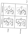
- Figure 2 shows the current paths in the cells 9 during normal operation.
- a cell can be in the inserted state or in the bypassed state.
- the cell In the bypassed state the cell is excluded from the power conversion function of a converter branch, which means that the energy storage component C of the cell is separated from the series connection of the cells.
- the cell In the inserted states the cell actively participates in the power conversion function of a converter branch. In this state, the energy storage component C is connected within the series connection of the cells.
- the cell can be in a charge mode or a discharge mode.
- the charge mode the energy storage component C accumulates electrical energy, which results in an increase of the charging state of the energy storage component C.
- the discharge mode accumulated electrical energy is drawn from the energy storage component C, such that the charging state of the energy storage component is reduced.
- the algorithm begins with a block 30 which simply says that the following blocks are repeatedly executed in the manner of an endless loop.
- the modulator for executing the power conversion function of a converter branch is performed.
- the aim of the modulator function is to synthesize the desired actual total voltage of a converter branch, namely the voltage v p , v n across the series connection of all cells 9 of a converter branch.
- the modulator function synthesizes a sinusoidal voltage over time Advanced methods as zero-sequence injection can be used in addition to increase the modulation range of the converter.
- the modulator in block 31 outputs the number of cells of a converter branch which shall be in the inserted state.
- decision block 32 a temporary variable z is generated as binary result of a comparison of the number of inserted cells of a converter branch in the inserted state in the current cycle (k) of the loop compared with the number of modules in the inserted state in the previous cycle (k-1) of the loop. If the number of cells in the inserted state remains the same from the previous cycle to the current cycle (then the difference is zero), then variable z is set to 0. Otherwise, z is unequal to 0.
- decision block 33 it is checked whether the converter branch is currently in the charge mode or in the discharge mode. This is checked by verifying the sign of the current i branch in the converter branch.
- decision block 37 it is checked whether the variable z is greater than 0. In such case the algorithm continues with block 38. Otherwise the algorithm continues with block 39.
- decision block 34 it is checked whether z is greater than 0. In such case the algorithm continues with block 35, otherwise the algorithm continues with block 36.
- blocks 35 and 38 the steps of calculating and sorting are performed, based on a cost function c 1 or c 3 .
- signals for generating commands for switching one or several cells in the inserted state are generated based upon the minimum of the cost function c 1 , c 3 .
- the minimum occurring cost function values in each branch can be determined by sorting all values or by sorting all values as far as possible to limit the computation time.
- blocks 36, 39 the steps of calculating and sorting are performed, based on a cost function c 2 or c 4 .
- signals for generating commands for switching a cell in the bypassed state are generated based upon the minimum of cost functions c 2 , c 4 .
- the algorithm proceeds after each of the steps 35, 36, 38, 39 again with block 31.
- the charging state v c of the energy storage element C of a cell 9 can be assessed, for example, by its voltage state.
- the cost functions c 1 , c 2 , c 3 , c 4 are established separately for each cell 9 of a converter branch.
- the value v c,min is the smallest value of all charging states v c of the cells of a converter branch.
- the value v c,max is the highest value of all charging states v c of the cells of the converter branch.
- the calculation and sorting step and the assignment of the signals for commanding the inserted state or the bypassed state can be done by seeking the minimum of all c 1 values of the cells of a converter branch.
- the calculation and sorting step and the step of generating a signal for commanding the inserted state or the bypassed state can be done by seeking the minimum of all c 2 values of the cells of a converter branch.
- the calculation and sorting step and the step of generating a signal for commanding the inserted state or the bypassed state can be done by seeking the minimum of all c 3 values of the cells of a converter branch.
- the calculation and sorting step and the step of generating a signal for commanding the inserted state or the bypassed state can be done by seeking the minimum of all c 4 values of the cells of a converter branch.
- P c is an example for a strain parameter, e.g. the electrical power dissipation loss of the energy storage component C of a cell 9.
- P c,min is the smallest value of the P c values of all cells of the converter branch.
- P c,max is the highest value of all P c values of the cells of the converter branch.
- ⁇ 1,A , ⁇ 2,A , ⁇ 3,A and ⁇ 4,A are weighting factors which are used for weighting the strain parameters in the cost functions. The ⁇ factors can be chosen individually for the cost functions.
- the electrical power dissipation loss of the energy storage component C can be measured by using measured current or voltage of the energy storage element. Both, the current through each branch and the charging state of each energy storage element are measured for proper control of the system. Consequently, the invention doesn't require any additional sensor effort.
- the measurement can be performed over a defined time frame such that an average value of the electrical power dissipation loss can be calculated over this time frame.
- the electrical power dissipation loss P c can be approximated by the integral of the square of the charging current of the energy storage component, and by assuming a proportional characteristic of such calculated value to the electrical loss resistance of the energy storage component.
- the frequency dependence of the electrical loss resistance of the energy storage component can be included, by also taking into account the harmonic spectra of the energy storage current.
- the electrical loss resistance values of the energy storage components could vary among different production processes and over the lifetime of the component, which could increase the unbalanced strain of the energy storage components among the cells of a converter branch.
- the actual value of the electrical loss resistance of an energy storage component is repeatedly determined, e.g. during runtime of the modular multilevel power converter, and is then used in the procedure as described before.
- Another strain parameter of the energy storage component which could be included as an input variable in the method of the invention is the temperature of the energy storage component.
- the temperature could be measured by a temperature sensor.
- the temperature of the energy storage component could be calculated based upon a thermodynamic model of the energy storage component and its integration in the cell, and using the electrical power dissipation loss P c of the energy storage component. If the temperature of the energy storage component is used for balancing the strain parameter, the cost functions could be established as follows.
- T c is the actual (estimated or measured) temperature of the energy storage component.
- T c,min is the lowest value of all T c values of the energy storage components of the cells of a converter branch.
- T c,max is the highest value of all T c values.
- ⁇ 1,B , ⁇ 2,B , ⁇ 3,B , ⁇ 4,B are further weighting factors.
- a further possible input variable of the cost functions can be one or more strain parameters of semiconductor components of the cells, like the electrical power dissipation loss and/or the temperature of the power semiconductor component.
- P v,D1 is the electrical power dissipation loss of diode D 1 .
- P v,T2 is the electrical power dissipation loss of transistor T 2
- P v,T1 is the electrical power dissipation loss of transistor T 1 .
- P v,D2 is the electrical power dissipation loss of diode D 2 .
- P v,max,D1 , P v,max,T2 , P v,max,T1 and P v,max,D2 are the corresponding maximum values across the cells of the converter branch.
- ⁇ 1 , ⁇ 2 , ⁇ 3 and ⁇ 4 are further weighting factors for the strain parameters.
- weighting factors ⁇ and ⁇ it is possible to balance the strain of the energy storage component and the power semiconductor components among the cells of a converter branch and within a cell.
- a further strain parameter of the energy storage component which can be incorporated in the cost functions is the storage capacity.
- the actual value of the storage capacity is another important factor which may result in an unbalanced stress of the cells and their energy storage components. The reason for such unbalanced strain may be unavoidable tolerances in the storage capacity, due to manufacturing and aging processes. Differences in the storage capacities of the energy storage component of the series connection of the cells result in differences in the charging times. According to a further embodiment of the invention, it is proposed to determine the actual storage capacity of the energy storage component of a cell during runtime of the modular multilevel power converter. The actual value of the energy storage capacity can be determined for example by integrating the charging current or discharging current over the times of the inserted state of the cell.
- the determined actual storage capacity of the energy storage component can be included in the cost functions, for example, by using the energy storage capacity or its reciprocal value as weighting factor in the cost function, for example as weighting factor for the input variable energy storage charging state, or by dividing another weighting factor of the energy storage charging state by this energy storage capacity.
Landscapes
- Engineering & Computer Science (AREA)
- Power Engineering (AREA)
- Charge And Discharge Circuits For Batteries Or The Like (AREA)
Claims (5)
- Procédé de sélection de cellules (9) d'un convertisseur de puissance modulaire multiniveau en fonction d'un stockage d'énergie et d'un semi-conducteur, qui comprend dans chacune d'une de multiples branches de convertisseur (1, 2, 3, 4, 5, 6) une pluralité de cellules (9) qui sont connectées en série, dans lequel chaque cellule (9) est commutée de manière répétitive à l'intérieur d'intervalles temporels réguliers ou irréguliers jusque dans un état d'insertion, dans lequel la cellule (9) est insérée activement dans la branche de convertisseur (1, 2, 3, 4, 5, 6), ou si dans un état de by-pass, dans lequel la cellule (9) est inactive, dans lequel l'état de chargement du composant de stockage d'énergie (C) des cellules (9) est équilibré parmi les cellules (9) d'une branche de convertisseur (1, 2, 3, 4, 5, 6) en générant des signaux pour ordonner soit l'état d'insertion soit l'état de by-pass pour chaque cellule (9) de la branche de convertisseur (1, 2, 3, 4, 5, 6) au moyen d'un algorithme d'équilibrage d'état de chargement de stockage d'énergie, dans lequel
au moins un paramètre de contrainte d'un composant de stockage d'énergie (C) de chacune des cellules (9) qui n'est pas l'état de chargement ou une quantité qui caractérise d'état de chargement du composant de stockage d'énergie (C), est équilibré parmi les cellules (5) d'une branche de convertisseur (1, 2, 3, 4, 5, 6) en générant des signaux pour ordonner soit l'état d'insertion soit l'état de by-pass pour chaque cellule (9) de la branche de convertisseur (1, 2, 3, 4, 5, 6) au moyen d'un algorithme d'équilibrage de paramètre de contrainte, dans lequel ledit au moins un paramètre de contrainte du composant de stockage d'énergie (C) est la perte par dissipation de puissance électrique du composant de stockage d'énergie (C), la résistance en série équivalente et l'impédance thermique du composant de stockage d'énergie, la capacité de stockage du composant de stockage d'énergie et/ou la température de point chaud du composant de stockage d'énergie (C) de la cellule (9), dans lequel la génération des signaux pour ordonner l'état d'insertion ou l'état de by-pass est effectuée en utilisant une fonction de coût (C1, C2, C3, C4) qui est calculée individuellement pour chacune des cellules (9), dans lequel la fonction de coût (C1, C2, C3, C4) a, en tant que variables d'entrée, un état de chargement mesuré du composant de stockage d'énergie (C) de la cellule (9) et au moins un paramètre de contrainte réel du composant de stockage d'énergie (C) de la cellule (9), qui est calculé/mesuré, dans lequel une variable d'entrée supplémentaire de la fonction de coût (C1, C2, C3, C4) est au moins un paramètre de contrainte d'un composant semi-conducteur de puissance (T1, T2, D1, D2) de la cellule (9), dans lequel les signaux pour ordonner état d'insertion ou l'état de by-pass sont générés en minimisant la fonction de coût (C1, C2, C3, C4) de la cellule correspondante (9), dans lequel plusieurs paramètres de contrainte du composant d'énergie de stockage (C) et du composant semi-conducteur de puissance (T1, T2, T3, T4) sont pondérés à l'intérieur de la fonction de coût (C1, C2, C3, C4) en utilisant des facteurs de pondération individuels pour chaque paramètre de contrainte, dans lequel les facteurs de pondération sont modifiés avec adaptation pendant le temps de fonctionnement du convertisseur de puissance modulaire multiniveau en dépendance d'estimations de cycle de vie d'un composant (C, T1, T2, D1, D2) de la cellule (9) associées au facteur de pondération, de telle sorte que la fin de la durée de vie du composant (C, T1, T2, D1, D2) associée au facteur de pondération est postposée. - Procédé selon la revendication 1, caractérisé en ce qu'une variable d'entrée supplémentaire de la fonction de coût (C1, C2, C3, C4) est le minimum ou le maximum de l'état de chargement du composant de stockage d'énergie (C) de toutes les cellules (9) de la branche de convertisseur (1, 2, 3, 4, 5, 6).
- Procédé selon la revendication 1, caractérisé en ce que ledit au moins un paramètre de contrainte du composant semi-conducteur de puissance (T1, T2, D1, D2) est la perte par dissipation de puissance électrique moyennée sur une durée spécifique et/ou la température et/ou la tension cumulée et/ou la durée de vie attendue du composant semi-conducteur de puissance (T1, T2, D1, D2).
- Programme d'ordinateur comprenant un code de programme qui, quand le code programme est exécuté sur un ordinateur (11) d'un convertisseur de puissance modulaire multiniveau, amène le convertisseur de puissance modulaire multiniveau à exécuter un procédé selon l'une quelconque des revendications précédentes.
- Convertisseur de puissance modulaire multiniveau, qui comprend dans chacune d'une ou de multiples branches de convertisseur (1, 2, 3, 4, 5, 6) une pluralité de cellules (9) qui sont connectées en série, et avec au moins une unité de gestion (10), qui est agencée pour générer des signaux pour ordonner soit l'état insertion soit l'état de by-pass pour chaque cellule (9) d'au moins une branche de convertisseur (1, 2, 3, 4, 5, 6), dans lequel l'unité de gestion (10) comprend au moins un ordinateur (11) et un composant de mémoire (12), dans lequel un programme d'ordinateur est stocké dans le composant de mémoire (12), qui est agencé pour exécuter un procédé selon l'une quelconque des revendications 1 à 3, si le code de programme du programme d'ordinateur est exécuté sur l'ordinateur (11).
Priority Applications (1)
| Application Number | Priority Date | Filing Date | Title |
|---|---|---|---|
| EP19191475.3A EP3780376B1 (fr) | 2019-08-13 | 2019-08-13 | Stockage d'énergie et sélection associée à un semiconducteur de cellules dans des convertisseurs de puissance multiniveau modulaires et programme informatique |
Applications Claiming Priority (1)
| Application Number | Priority Date | Filing Date | Title |
|---|---|---|---|
| EP19191475.3A EP3780376B1 (fr) | 2019-08-13 | 2019-08-13 | Stockage d'énergie et sélection associée à un semiconducteur de cellules dans des convertisseurs de puissance multiniveau modulaires et programme informatique |
Publications (2)
| Publication Number | Publication Date |
|---|---|
| EP3780376A1 EP3780376A1 (fr) | 2021-02-17 |
| EP3780376B1 true EP3780376B1 (fr) | 2024-03-20 |
Family
ID=67620322
Family Applications (1)
| Application Number | Title | Priority Date | Filing Date |
|---|---|---|---|
| EP19191475.3A Active EP3780376B1 (fr) | 2019-08-13 | 2019-08-13 | Stockage d'énergie et sélection associée à un semiconducteur de cellules dans des convertisseurs de puissance multiniveau modulaires et programme informatique |
Country Status (1)
| Country | Link |
|---|---|
| EP (1) | EP3780376B1 (fr) |
Families Citing this family (1)
| Publication number | Priority date | Publication date | Assignee | Title |
|---|---|---|---|---|
| CN114593505B (zh) * | 2022-03-29 | 2023-08-29 | 海南省电力学校(海南省电力技工学校) | 一种基于二阶等效热参数模型的变频空调负荷虚拟储能建模方法 |
Family Cites Families (2)
| Publication number | Priority date | Publication date | Assignee | Title |
|---|---|---|---|---|
| CN104396136B (zh) * | 2012-07-06 | 2016-03-30 | Abb技术有限公司 | 控制模块化转换器 |
| WO2018099564A1 (fr) * | 2016-12-01 | 2018-06-07 | Abb Schweiz Ag | Procédé de sélection de cellule dans un convertisseur modulaire multiniveaux |
-
2019
- 2019-08-13 EP EP19191475.3A patent/EP3780376B1/fr active Active
Non-Patent Citations (2)
| Title |
|---|
| HAHN FREDERIK ET AL: "Enhanced Current Capability for Modular Multilevel Converters by a Combined Sorting Algorithm for Capacitor Voltages and Semiconductor Losses", 2019 IEEE APPLIED POWER ELECTRONICS CONFERENCE AND EXPOSITION (APEC), IEEE, 17 March 2019 (2019-03-17), pages 3071 - 3077, XP033555109, DOI: 10.1109/APEC.2019.8722065 * |
| TANAKA TAKAAKI ET AL: "Asymmetrical Reactive Power Capability of Modular Multilevel Cascade Converter Based STATCOMs for Offshore Wind Farm", IEEE TRANSACTIONS ON POWER ELECTRONICS, INSTITUTE OF ELECTRICAL AND ELECTRONICS ENGINEERS, USA, vol. 34, no. 6, 1 June 2019 (2019-06-01), pages 5147 - 5164, XP011721368, ISSN: 0885-8993, [retrieved on 20190422], DOI: 10.1109/TPEL.2018.2866398 * |
Also Published As
| Publication number | Publication date |
|---|---|
| EP3780376A1 (fr) | 2021-02-17 |
Similar Documents
| Publication | Publication Date | Title |
|---|---|---|
| US11152797B2 (en) | DC charging of an intelligent battery | |
| US10305298B2 (en) | Method and apparatus for creating a dynamically reconfigurable energy storage device | |
| KR101452778B1 (ko) | 축전장치의 충전제어방법 및 방전제어방법 | |
| US10848098B2 (en) | Smart energy storage system | |
| US10637251B2 (en) | Modular energy storage direct converter system | |
| ES2394629T3 (es) | Dispositivo de almacenamiento de carga que usa condensadores y su método de control | |
| US8288992B2 (en) | Cell management system | |
| Kim et al. | A series-connected self-reconfigurable multicell battery capable of safe and effective charging/discharging and balancing operations | |
| US20170093187A1 (en) | Energy storage system | |
| KR20110139244A (ko) | 지능형 에너지 스토리지 팩의 스케일러블한 구성을 위한 시스템 및 방법 | |
| US20150069844A1 (en) | Power storage module and power storage device | |
| US20220344947A1 (en) | Energy storage system, balancing control method for energy storage system, and photovoltaic power system | |
| US20110140535A1 (en) | Power converting device for new renewable energy storage system | |
| Cao et al. | Evaluation of bi‐directional single‐inductor multi‐input battery system with state‐of‐charge balancing control | |
| JP2013085459A (ja) | 電力貯蔵システムおよびその制御方法 | |
| US20130141048A1 (en) | Battery management system | |
| Shenoy et al. | Differential power processing architecture for increased energy production and reliability of photovoltaic systems | |
| CN113541268B (zh) | 一种储能系统及其控制方法 | |
| Shadmand et al. | Auto-tuning the cost function weight factors in a model predictive controller for a matrix converter VAR compensator | |
| JP7406933B2 (ja) | 蓄電システム | |
| Tajeddine et al. | A cascaded h-bridge multilevel inverter with soc battery balancing | |
| EP3780376B1 (fr) | Stockage d'énergie et sélection associée à un semiconducteur de cellules dans des convertisseurs de puissance multiniveau modulaires et programme informatique | |
| WO2011132302A1 (fr) | Procédé de commande de charge et procédé de commande de décharge pour dispositif accumulateur électrique | |
| US20240088700A1 (en) | Battery management controllers and associated methods | |
| US20170179739A1 (en) | System and Method for Protecting Energy Storage Systems from Overcurrent Conditions |
Legal Events
| Date | Code | Title | Description |
|---|---|---|---|
| PUAI | Public reference made under article 153(3) epc to a published international application that has entered the european phase |
Free format text: ORIGINAL CODE: 0009012 |
|
| STAA | Information on the status of an ep patent application or granted ep patent |
Free format text: STATUS: THE APPLICATION HAS BEEN PUBLISHED |
|
| AK | Designated contracting states |
Kind code of ref document: A1 Designated state(s): AL AT BE BG CH CY CZ DE DK EE ES FI FR GB GR HR HU IE IS IT LI LT LU LV MC MK MT NL NO PL PT RO RS SE SI SK SM TR |
|
| AX | Request for extension of the european patent |
Extension state: BA ME |
|
| STAA | Information on the status of an ep patent application or granted ep patent |
Free format text: STATUS: REQUEST FOR EXAMINATION WAS MADE |
|
| STAA | Information on the status of an ep patent application or granted ep patent |
Free format text: STATUS: EXAMINATION IS IN PROGRESS |
|
| 17P | Request for examination filed |
Effective date: 20210811 |
|
| RBV | Designated contracting states (corrected) |
Designated state(s): AL AT BE BG CH CY CZ DE DK EE ES FI FR GB GR HR HU IE IS IT LI LT LU LV MC MK MT NL NO PL PT RO RS SE SI SK SM TR |
|
| 17Q | First examination report despatched |
Effective date: 20210906 |
|
| GRAP | Despatch of communication of intention to grant a patent |
Free format text: ORIGINAL CODE: EPIDOSNIGR1 |
|
| STAA | Information on the status of an ep patent application or granted ep patent |
Free format text: STATUS: GRANT OF PATENT IS INTENDED |
|
| INTG | Intention to grant announced |
Effective date: 20231103 |
|
| GRAS | Grant fee paid |
Free format text: ORIGINAL CODE: EPIDOSNIGR3 |
|
| GRAA | (expected) grant |
Free format text: ORIGINAL CODE: 0009210 |
|
| STAA | Information on the status of an ep patent application or granted ep patent |
Free format text: STATUS: THE PATENT HAS BEEN GRANTED |
|
| REG | Reference to a national code |
Ref country code: DE Ref legal event code: R081 Ref document number: 602019048509 Country of ref document: DE Owner name: CHRISTIAN-ALBRECHTS-UNIVERSITAET ZU KIEL, KOER, DE Free format text: FORMER OWNER: ANMELDERANGABEN UNKLAR / UNVOLLSTAENDIG, 80297 MUENCHEN, DE |
|
| AK | Designated contracting states |
Kind code of ref document: B1 Designated state(s): AL AT BE BG CH CY CZ DE DK EE ES FI FR GB GR HR HU IE IS IT LI LT LU LV MC MK MT NL NO PL PT RO RS SE SI SK SM TR |
|
| REG | Reference to a national code |
Ref country code: GB Ref legal event code: FG4D |
|
| REG | Reference to a national code |
Ref country code: CH Ref legal event code: EP |
|
| REG | Reference to a national code |
Ref country code: DE Ref legal event code: R096 Ref document number: 602019048509 Country of ref document: DE |
|
| REG | Reference to a national code |
Ref country code: IE Ref legal event code: FG4D |
|
| U01 | Request for unitary effect filed |
Effective date: 20240416 |