EP3779949A1 - Fully differential front end for sensing - Google Patents
Fully differential front end for sensing Download PDFInfo
- Publication number
- EP3779949A1 EP3779949A1 EP20156633.8A EP20156633A EP3779949A1 EP 3779949 A1 EP3779949 A1 EP 3779949A1 EP 20156633 A EP20156633 A EP 20156633A EP 3779949 A1 EP3779949 A1 EP 3779949A1
- Authority
- EP
- European Patent Office
- Prior art keywords
- pixel
- current
- input
- circuit
- low
- Prior art date
- Legal status (The legal status is an assumption and is not a legal conclusion. Google has not performed a legal analysis and makes no representation as to the accuracy of the status listed.)
- Granted
Links
Images







Classifications
-
- G—PHYSICS
- G09—EDUCATION; CRYPTOGRAPHY; DISPLAY; ADVERTISING; SEALS
- G09G—ARRANGEMENTS OR CIRCUITS FOR CONTROL OF INDICATING DEVICES USING STATIC MEANS TO PRESENT VARIABLE INFORMATION
- G09G3/00—Control arrangements or circuits, of interest only in connection with visual indicators other than cathode-ray tubes
- G09G3/006—Electronic inspection or testing of displays and display drivers, e.g. of LED or LCD displays
-
- G—PHYSICS
- G09—EDUCATION; CRYPTOGRAPHY; DISPLAY; ADVERTISING; SEALS
- G09G—ARRANGEMENTS OR CIRCUITS FOR CONTROL OF INDICATING DEVICES USING STATIC MEANS TO PRESENT VARIABLE INFORMATION
- G09G3/00—Control arrangements or circuits, of interest only in connection with visual indicators other than cathode-ray tubes
- G09G3/20—Control arrangements or circuits, of interest only in connection with visual indicators other than cathode-ray tubes for presentation of an assembly of a number of characters, e.g. a page, by composing the assembly by combination of individual elements arranged in a matrix no fixed position being assigned to or needed to be assigned to the individual characters or partial characters
- G09G3/22—Control arrangements or circuits, of interest only in connection with visual indicators other than cathode-ray tubes for presentation of an assembly of a number of characters, e.g. a page, by composing the assembly by combination of individual elements arranged in a matrix no fixed position being assigned to or needed to be assigned to the individual characters or partial characters using controlled light sources
- G09G3/30—Control arrangements or circuits, of interest only in connection with visual indicators other than cathode-ray tubes for presentation of an assembly of a number of characters, e.g. a page, by composing the assembly by combination of individual elements arranged in a matrix no fixed position being assigned to or needed to be assigned to the individual characters or partial characters using controlled light sources using electroluminescent panels
- G09G3/32—Control arrangements or circuits, of interest only in connection with visual indicators other than cathode-ray tubes for presentation of an assembly of a number of characters, e.g. a page, by composing the assembly by combination of individual elements arranged in a matrix no fixed position being assigned to or needed to be assigned to the individual characters or partial characters using controlled light sources using electroluminescent panels semiconductive, e.g. using light-emitting diodes [LED]
-
- G—PHYSICS
- G09—EDUCATION; CRYPTOGRAPHY; DISPLAY; ADVERTISING; SEALS
- G09G—ARRANGEMENTS OR CIRCUITS FOR CONTROL OF INDICATING DEVICES USING STATIC MEANS TO PRESENT VARIABLE INFORMATION
- G09G3/00—Control arrangements or circuits, of interest only in connection with visual indicators other than cathode-ray tubes
- G09G3/20—Control arrangements or circuits, of interest only in connection with visual indicators other than cathode-ray tubes for presentation of an assembly of a number of characters, e.g. a page, by composing the assembly by combination of individual elements arranged in a matrix no fixed position being assigned to or needed to be assigned to the individual characters or partial characters
- G09G3/22—Control arrangements or circuits, of interest only in connection with visual indicators other than cathode-ray tubes for presentation of an assembly of a number of characters, e.g. a page, by composing the assembly by combination of individual elements arranged in a matrix no fixed position being assigned to or needed to be assigned to the individual characters or partial characters using controlled light sources
- G09G3/30—Control arrangements or circuits, of interest only in connection with visual indicators other than cathode-ray tubes for presentation of an assembly of a number of characters, e.g. a page, by composing the assembly by combination of individual elements arranged in a matrix no fixed position being assigned to or needed to be assigned to the individual characters or partial characters using controlled light sources using electroluminescent panels
- G09G3/32—Control arrangements or circuits, of interest only in connection with visual indicators other than cathode-ray tubes for presentation of an assembly of a number of characters, e.g. a page, by composing the assembly by combination of individual elements arranged in a matrix no fixed position being assigned to or needed to be assigned to the individual characters or partial characters using controlled light sources using electroluminescent panels semiconductive, e.g. using light-emitting diodes [LED]
- G09G3/3208—Control arrangements or circuits, of interest only in connection with visual indicators other than cathode-ray tubes for presentation of an assembly of a number of characters, e.g. a page, by composing the assembly by combination of individual elements arranged in a matrix no fixed position being assigned to or needed to be assigned to the individual characters or partial characters using controlled light sources using electroluminescent panels semiconductive, e.g. using light-emitting diodes [LED] organic, e.g. using organic light-emitting diodes [OLED]
- G09G3/3225—Control arrangements or circuits, of interest only in connection with visual indicators other than cathode-ray tubes for presentation of an assembly of a number of characters, e.g. a page, by composing the assembly by combination of individual elements arranged in a matrix no fixed position being assigned to or needed to be assigned to the individual characters or partial characters using controlled light sources using electroluminescent panels semiconductive, e.g. using light-emitting diodes [LED] organic, e.g. using organic light-emitting diodes [OLED] using an active matrix
- G09G3/3233—Control arrangements or circuits, of interest only in connection with visual indicators other than cathode-ray tubes for presentation of an assembly of a number of characters, e.g. a page, by composing the assembly by combination of individual elements arranged in a matrix no fixed position being assigned to or needed to be assigned to the individual characters or partial characters using controlled light sources using electroluminescent panels semiconductive, e.g. using light-emitting diodes [LED] organic, e.g. using organic light-emitting diodes [OLED] using an active matrix with pixel circuitry controlling the current through the light-emitting element
-
- G—PHYSICS
- G09—EDUCATION; CRYPTOGRAPHY; DISPLAY; ADVERTISING; SEALS
- G09G—ARRANGEMENTS OR CIRCUITS FOR CONTROL OF INDICATING DEVICES USING STATIC MEANS TO PRESENT VARIABLE INFORMATION
- G09G3/00—Control arrangements or circuits, of interest only in connection with visual indicators other than cathode-ray tubes
- G09G3/20—Control arrangements or circuits, of interest only in connection with visual indicators other than cathode-ray tubes for presentation of an assembly of a number of characters, e.g. a page, by composing the assembly by combination of individual elements arranged in a matrix no fixed position being assigned to or needed to be assigned to the individual characters or partial characters
- G09G3/22—Control arrangements or circuits, of interest only in connection with visual indicators other than cathode-ray tubes for presentation of an assembly of a number of characters, e.g. a page, by composing the assembly by combination of individual elements arranged in a matrix no fixed position being assigned to or needed to be assigned to the individual characters or partial characters using controlled light sources
- G09G3/30—Control arrangements or circuits, of interest only in connection with visual indicators other than cathode-ray tubes for presentation of an assembly of a number of characters, e.g. a page, by composing the assembly by combination of individual elements arranged in a matrix no fixed position being assigned to or needed to be assigned to the individual characters or partial characters using controlled light sources using electroluminescent panels
- G09G3/32—Control arrangements or circuits, of interest only in connection with visual indicators other than cathode-ray tubes for presentation of an assembly of a number of characters, e.g. a page, by composing the assembly by combination of individual elements arranged in a matrix no fixed position being assigned to or needed to be assigned to the individual characters or partial characters using controlled light sources using electroluminescent panels semiconductive, e.g. using light-emitting diodes [LED]
- G09G3/3208—Control arrangements or circuits, of interest only in connection with visual indicators other than cathode-ray tubes for presentation of an assembly of a number of characters, e.g. a page, by composing the assembly by combination of individual elements arranged in a matrix no fixed position being assigned to or needed to be assigned to the individual characters or partial characters using controlled light sources using electroluminescent panels semiconductive, e.g. using light-emitting diodes [LED] organic, e.g. using organic light-emitting diodes [OLED]
- G09G3/3275—Details of drivers for data electrodes
-
- G—PHYSICS
- G09—EDUCATION; CRYPTOGRAPHY; DISPLAY; ADVERTISING; SEALS
- G09G—ARRANGEMENTS OR CIRCUITS FOR CONTROL OF INDICATING DEVICES USING STATIC MEANS TO PRESENT VARIABLE INFORMATION
- G09G2310/00—Command of the display device
- G09G2310/02—Addressing, scanning or driving the display screen or processing steps related thereto
- G09G2310/0264—Details of driving circuits
- G09G2310/0297—Special arrangements with multiplexing or demultiplexing of display data in the drivers for data electrodes, in a pre-processing circuitry delivering display data to said drivers or in the matrix panel, e.g. multiplexing plural data signals to one D/A converter or demultiplexing the D/A converter output to multiple columns
-
- G—PHYSICS
- G09—EDUCATION; CRYPTOGRAPHY; DISPLAY; ADVERTISING; SEALS
- G09G—ARRANGEMENTS OR CIRCUITS FOR CONTROL OF INDICATING DEVICES USING STATIC MEANS TO PRESENT VARIABLE INFORMATION
- G09G2320/00—Control of display operating conditions
- G09G2320/02—Improving the quality of display appearance
- G09G2320/029—Improving the quality of display appearance by monitoring one or more pixels in the display panel, e.g. by monitoring a fixed reference pixel
-
- G—PHYSICS
- G09—EDUCATION; CRYPTOGRAPHY; DISPLAY; ADVERTISING; SEALS
- G09G—ARRANGEMENTS OR CIRCUITS FOR CONTROL OF INDICATING DEVICES USING STATIC MEANS TO PRESENT VARIABLE INFORMATION
- G09G2320/00—Control of display operating conditions
- G09G2320/02—Improving the quality of display appearance
- G09G2320/029—Improving the quality of display appearance by monitoring one or more pixels in the display panel, e.g. by monitoring a fixed reference pixel
- G09G2320/0295—Improving the quality of display appearance by monitoring one or more pixels in the display panel, e.g. by monitoring a fixed reference pixel by monitoring each display pixel
-
- G—PHYSICS
- G09—EDUCATION; CRYPTOGRAPHY; DISPLAY; ADVERTISING; SEALS
- G09G—ARRANGEMENTS OR CIRCUITS FOR CONTROL OF INDICATING DEVICES USING STATIC MEANS TO PRESENT VARIABLE INFORMATION
- G09G2320/00—Control of display operating conditions
- G09G2320/04—Maintaining the quality of display appearance
- G09G2320/043—Preventing or counteracting the effects of ageing
-
- G—PHYSICS
- G09—EDUCATION; CRYPTOGRAPHY; DISPLAY; ADVERTISING; SEALS
- G09G—ARRANGEMENTS OR CIRCUITS FOR CONTROL OF INDICATING DEVICES USING STATIC MEANS TO PRESENT VARIABLE INFORMATION
- G09G2330/00—Aspects of power supply; Aspects of display protection and defect management
- G09G2330/12—Test circuits or failure detection circuits included in a display system, as permanent part thereof
-
- G—PHYSICS
- G09—EDUCATION; CRYPTOGRAPHY; DISPLAY; ADVERTISING; SEALS
- G09G—ARRANGEMENTS OR CIRCUITS FOR CONTROL OF INDICATING DEVICES USING STATIC MEANS TO PRESENT VARIABLE INFORMATION
- G09G2380/00—Specific applications
- G09G2380/06—Remotely controlled electronic signs other than labels
Definitions
- One or more aspects of embodiments according to the present disclosure relate to displays, and more particularly to measuring pixel characteristics.
- a video display such as those used for computers or mobile devices may have a plurality of pixels, and, in each pixel, a plurality of transistors, including a drive transistor configured to control a drive current through a display element such as a light emitting diode (LED) (e.g., an organic light emitting diode (OLED)).
- LED light emitting diode
- OLED organic light emitting diode
- a system including: a first pixel; a second pixel; a differential sensing circuit; a reference current source; and a control circuit, the differential sensing circuit having a first input, a second input, and an output, the first input being connected to a node at which a reference current generated by the reference current source is subtracted from a first pixel current, the first pixel current including a current generated by the first pixel; the second input being configured to receive a second pixel current, the second pixel current including a current generated by the second pixel; the output being configured to produce an output signal based on a difference between a current received at the first input and a current received at the second input; the control circuit being configured to: cause the first pixel to be turned on; cause the second pixel to be turned off; and cause the reference current source to generate the reference current.
- the system includes a display panel including the first pixel and the second pixel, the first pixel is in a first column of the display panel, the second pixel is in a second column of the display panel, and the first pixel and the second pixel are adjacent, and in the same row of the display panel.
- the first pixel current further includes leakage currents from a plurality of pixels in the first column, other than the first pixel
- the second pixel current includes leakage currents from a plurality of pixels in the second column, other than the second pixel.
- the differential sensing circuit includes a low-pass current filter.
- the low-pass current filter includes a fully differential amplifier.
- the low-pass current filter further includes a common-mode feedback circuit with a bandwidth of at least 1 MHz.
- the differential sensing circuit further includes an integrator, connected to an output of the low-pass current filter.
- the system further includes a drive circuit, wherein a first conductor of the display panel is connected to the first pixel, the first conductor being configured: in a first state of the system, to carry the first pixel current, and in a second state of the system, to carry a current from the drive circuit to the first pixel.
- control circuit is configured, in the second state: to cause the low-pass current filter to operate in a reset state, and to cause the drive circuit to drive the first conductor to a reference voltage.
- a method for sensing a current in a display including: a first pixel; a second pixel; a differential sensing circuit; and a reference current source; the differential sensing circuit having a first input, a second input, and an output, the method including: feeding to the first input the difference between a first pixel current and a reference current generated by the reference current source, the first pixel current including a current generated by the first pixel; feeding to the second input a second pixel current, the second pixel current including a current generated by the second pixel; producing at the output an output signal based on a difference between the current received at the first input and the current received at the second input; turning the first pixel on; turning the second pixel off; and generating the reference current.
- the display includes a display panel including the first pixel and the second pixel, the first pixel is in a first column of the display panel, the second pixel is in a second column of the display panel, and the first pixel and the second pixel are adjacent, and in the same row of the display panel.
- the first pixel current further includes leakage currents from a plurality of pixels in the first column, other than the first pixel
- the second pixel current includes leakage currents from a plurality of pixels in the second column, other than the second pixel.
- the differential sensing circuit includes a low-pass current filter.
- the low-pass current filter includes a fully differential amplifier.
- the low-pass current filter further includes a common-mode feedback circuit with a bandwidth of at least 1 MHz.
- the differential sensing circuit further includes an integrator, connected to an output of the low-pass current filter.
- the display further includes a drive circuit, wherein a first conductor of the display panel is connected to the first pixel, the first conductor being configured: in a first state of the display, to carry the first pixel current, and in a second state of the display, to carry a current from the drive circuit to the first pixel.
- the method further includes, in the second state: operating the low-pass current filter in a reset state, and driving, by the drive circuit, the first conductor to a reference voltage.
- a system including: a first pixel; a second pixel; a differential sensing circuit; a reference current source; and means for controlling, the differential sensing circuit having a first input, a second input, and an output, the first input being connected to a node at which a reference current generated by the reference current source is subtracted from a first pixel current, the first pixel current including a current generated by the first pixel; the second input being configured to receive a second pixel current, the second pixel current including a current generated by the second pixel; the output being configured to produce an output signal based on a difference between a current received at the first input and a current received at the second input; the means for controlling being configured to: cause the first pixel to be turned on; cause the second pixel to be turned off; and cause the reference current source to generate the reference current.
- the system includes a display panel including the first pixel and the second pixel, the first pixel is in a first column of the display panel, the second pixel is in a second column of the display panel, the first pixel and the second pixel are adjacent, and in the same row of the display panel.
- a display e.g., a mobile device display
- a display may include a plurality of pixels arranged in rows and columns.
- Each pixel may be configured to produce light of one color (e.g., red, green or blue) and may be part of a composite pixel that includes, e.g., three such pixels.
- the composite pixel may be configured to produce any of a wide range of colors (in some contexts, what is referred to herein as a "pixel” is instead referred to as a "sub-pixel”, and what is referred to herein as a "composite pixel" is instead referred to as a "pixel").
- Each pixel may include a drive circuit, e.g., 7-transistor 1-capacitor (7T1C) drive circuit as shown on the left of FIG. 1 or a 4-transistor 1-capacitor (4T1C) drive circuit as shown at the bottom of FIG. 1 .
- a drive transistor 110 (the gate-source voltage of which is controlled by the capacitor 115) controls the current through the light emitting diode 120 when the pixel is emitting light.
- An upper pass-gate transistor 125 may be used to selectively connect the gate of the drive transistor 110 (and one terminal of the capacitor 115) to a power supply voltage.
- a lower pass-gate transistor 130 may be used to selectively connect a drive sense conductor 135 to a source node 140 (which is a node connected to the source of the drive transistor 110), to the anode of the light emitting diode 120 and to the other terminal of the capacitor 115.
- a pixel drive and sense circuit 145 may be connected to the drive sense conductor 135.
- the pixel drive and sense circuit 145 may include a drive amplifier and a sensing circuit, configured to be selectively connected, one at a time, to the drive sense conductor 135.
- current flows through the drive transistor 110, and the lower pass-gate transistor 130 is turned-off, disconnecting the drive sense conductor 135 from the source node 140, current may flow through the light emitting diode 120 causing it to emit light.
- the lower pass-gate transistor 130 is turned-on, and the drive sense conductor 135 is driven to a lower voltage than the cathode of the light emitting diode 120, the light emitting diode 120 may be reverse-biased.
- Any current flowing in the drive sense conductor 135 may flow to the pixel drive and sense circuit 145, where the current may be sensed.
- This sensed current may be compared to a desired current (e.g., the current that an ideal, or nominal transistor would drive at the same gate-source voltage), and to the extent that the sensed current differs from the ideal current, measures may be taken (e.g., the gate-source voltage may be adjusted) to compensate for the discrepancy.
- a desired current e.g., the current that an ideal, or nominal transistor would drive at the same gate-source voltage
- measures may be taken (e.g., the gate-source voltage may be adjusted) to compensate for the discrepancy.
- the current of any pixel may be sensed in a differential manner, for improved accuracy.
- the current driven by the drive transistor 110 of the pixel on the left of FIG. 2A (which may be referred to as an "odd” pixel) is to be sensed, it (“odd” pixel) may be turned-on (by charging capacitor of the odd pixel so as to turn on the drive transistor 110 of the odd pixel).
- the drive transistor 110 of the pixel on the right of FIG. 2A (which may be referred to as an "even” pixel) may be turned-off (by discharging the capacitor of the even pixel so as to turn off the drive transistor 110 of the even pixel).
- the difference between the two corresponding currents flowing out of two respective conductors may be measured.
- Each of the column conductors 205 may be connected to all of the pixels of a column of the display.
- the total leakage current in the other pixels may be significant.
- the leakage currents in the adjacent column containing the even pixel
- the contribution of the leakage currents to the current flowing in the column conductor connected to the odd pixel may be canceled when the difference between the currents in the two column conductors 205 is sensed.
- the SCAN1, SCAN2, and EMIT control lines may be per row, and may have different timing between rows. As mentioned above, differential sensing may be used, so that half the pixels in a row are sensed per operation. The same set of gate control signals may be applied to odd and even pixels, such that there is no distinction between odd and even pixels.
- Each digital to analog converter and associated drive amplifier 220 may be used both to drive a column conductor 205 to charge the capacitor of a pixel, and to generate the reference current when the current driven by the drive transistor 110 is being sensed; this may be accomplished using multiplexers, as shown.
- the embodiment of FIG. 1 does not include this feature and instead includes two separate digital to analog converters.
- the emit transistor of each pixel may remain turned-off.
- a respective VDRIVE may be stored across the pixel capacitor of each of the pixels.
- the source of the drive transistor 110 of the even pixel may be driven to ELVSS, so that it (the even pixel) will be turned-off, as mentioned above.
- the upper pass-gate transistors 125 ( FIG. 1 ) are turned-off so that the gates of the drive transistors 110 float, and so that the charge on the capacitor of each pixel remains constant.
- the source of the drive transistor 110 of each pixel is driven (e.g., to VREF, which may be slightly less than ELVSS) so that each light emitting diode 120 is reverse-biased, and so that no current flows through the light emitting diodes 120.
- each pixel is turned-on, and as a result of the light emitting diode 120 being reverse-biased, any current driven by the drive transistor 110 of a pixel flows through a respective column conductor 205 to the sensing circuit.
- the digital to analog converter and the drive amplifier 220 connected to it may generate the reference current IREF.
- ground noise (V g ) may be very large at low frequencies.
- pseudo-differential sensing sensing the difference between an on pixel and an off pixel, as described above, using a pseudo-differential front end
- C P column capacitance
- the common-mode current caused by the noise may be excessive and may increase the dynamic range requirements of the front end.
- this wideband thermal noise which may be generated by the resistance of the column conductor 205 (modeled, in FIG. 3C , by the resistance R P ) may be reduced by using a front end that is configured as, or includes, a low-pass filter, which may pass the (DC) signal (I pixel ) being sensed.
- a low-pass filter an integrator
- the front-end integrator may be reset prior to the sense operation.
- Each sense operation may be preceded by a drive operation during which the drive amplifier 220 ( FIGs. 2A-2C ) drives the column conductor 205 to a set voltage. Before a sense operation starts, the voltage on the column conductor 205 may be restored to VREF.
- Another issue of concern with the circuit of FIG. 3C may be that because the capacitance to ground of the column conductor 205 may be large, the sense amplifier (in reset mode) may require a long time to bring the voltage of the column conductor 205 to VREF.
- FIG. 4 shows a differential sensing circuit 400, with two inputs for sensing a difference between a current from a first pixel (e.g., the odd pixel of FIGs. 2A- 2C ) and a second pixel (e.g., the even pixel of FIGs. 2A- 2C ) (each current having subtracted from it a respective reference current).
- the differential sensing circuit has a two-stage architecture with a low-pass current filter 405 (e.g., a first integrator, as shown) as the first stage, and an integrator 410 (e.g., a second integrator, as shown) as the second stage.
- the integrator 410 may be coupled to the low-pass current filter 405 by two mirroring capacitors 425.
- Each of the low-pass current filter 405 and the integrator 410 may include a fully differential operational amplifier with a capacitor (or “feedback capacitor”) in each feedback path.
- the circuit may be used to perform differential sensing between two adjacent pixels (e.g. a red pixel and a green pixel of a composite pixel containing three pixels, a red pixel, a green pixel, and a blue pixel, or a green pixel and a blue pixel of a composite pixel).
- a wideband common mode feedback amplifier 415 (which may have an open loop bandwidth of between 10 MHz and 100 MHz) feeds back around the low-pass current filter 405.
- the circuit of FIG. 4 shows both the drive amplifier 220 and the differential sensing circuit 400 simultaneously connected to the pixels 420 through respective resistor-capacitor networks used to model the column conductors 205. In some embodiments, however, there is only one column conductor 205 per pixel, and either the drive amplifier 220 or the differential sensing circuit 400 is connected to the column conductor 205 at any time (as shown in FIGs. 2A-2C , in which multiplexers are used to select whether the drive amplifier 220 or the differential sensing circuit is connected to the column conductor 205 at any time).
- the low-pass current filter 405 and the integrator 410 may be fully differential.
- a fully differential circuit is one that (unlike a single-ended or pseudo-differential amplifier) does not compare the signal to ground. Instead, each differential gain stage in a fully differential amplifier, for example, compares the two signals being processed directly to each other.
- the wideband common mode feedback amplifier 415 may compute the common mode output signal at the output of the low-pass current filter 405 (e.g., it may compute the average of the voltages at the two output conductors using a resistor network), and feed back to a common mode input in the low-pass current filter 405.
- the common mode input may be, for example, (i) a gate of a current source (or “tail current source") connected to the two sources of a differential pair in the low-pass current filter 405, or (ii) a node connected to two corresponding transistors in the load network of a differential pair in the low-pass current filter 405.
- the performance of the circuit of FIG. 4 may be superior to that of a pseudo-differential circuit (e.g., as illustrated in FIG. 3B ). This may be shown as follows.
- v 1 ⁇ v 2 v g R d ⁇ R 2 R 1 + R 2 + R d R 1 + R 2 ⁇ + R d and v 1 ⁇ v 2 v g ⁇ R d ⁇ R 2 R 1 + R 2 + R d 2 .
- FIG. 5C shows a circuit that may be used to analyze the low-pass current filter 405 of FIG. 4 .
- ⁇ i 1 v 1 ⁇ v 2 R d + v 1 R CM
- the differential impedance looking into the input terminals may be that of a large capacitor C i * A (the operational amplifier may cause the relatively small capacitor C i to look much larger, i.e., to make it look like C i * A). It may be advantageous for this apparent size to be significantly larger than the capacitance of the channel itself, i.e., for the impedance looking into the low-pass current filter to be significantly smaller than the impedance of the channel itself. In this circumstance, the bulk of the current driven by the drive transistor 110 flows into the low-pass current filter. For frequencies between f 3 dB and f ug , the differential impedance looking into the input terminals may have the characteristics of a resistor.
- FIG. 6 shows a flow chart of a method for sensing, using the circuits described herein.
- the odd pixel is driven with the desired V gs for sensing, and the even pixel is driven with the V gs corresponding to black (no emission from the light emitting diode 120).
- the upper pass-gate transistor 125 of each pixel is turned off, and both pixels are driven with the V gs corresponding to black, to reset the column conductors 205 (this drive step does not affect the charges on the capacitors of the pixels, because the upper pass-gate transistor 125 of each pixel is turned-off).
- the circuit enters sense mode.
- the front end is in reset, i.e., switches (e.g., transistor switches) connected across the feedback capacitors of the low-pass current filter 405 and the integrator 410 are closed (e.g., the transistors are turned on) so that these capacitors become, and remain, discharged during the reset.
- the circuit may stay in reset mode until the sense front-end voltage and the voltage on the column conductors 205 equalize; the effect of this state may be to sample the front end offset.
- the reset mode enables the column conductor 205 to equalize with a reference voltage.
- the pixel current may be turned on or off (i.e., the control signal EMIT_ENB may be either high level or low level) during the reset phase.
- the front end is released from reset (e.g., the transistors connected across the feedback capacitors are turned-off), and integration (of the sensed current) begins.
- the output of the integrator 410 is sampled.
- the reference voltage or reference current provided by a current source
- FIG. 7 is a timing diagram showing control signals for cycling through the states illustrated in FIG. 6 .
- the reference symbols of FIG. 6 are repeated to show the correspondence between the steps of FIG. 6 and time intervals in FIG. 7 .
- Further features, not shown in FIG. 7 may be present in some embodiments.
- a wait state 705 in which the low-pass current filter 405 is released from reset and allowed to settle, while the integrator 410 remains in reset mode
- the integrating state 620 which may begin correspondingly later.
- the integrating state is divided into two portions. In one portion, the currents from both the even and odd pixels are turned-off (by turning off the lower pass-gate transistors 130, using the SCAN2_EN control signal).
- the even and odd pixels are turned-on (by turning on the lower pass-gate transistors 130, using the SCAN2_EN control signal).
- the polarity of the connection between the low-pass current filter 405 and the integrator 410 may be reversed, so that the output of the integrator, at the end of the second portion, may be the difference between the current when the pixels are on and the current when the pixels are off (the latter of which may include contributions (e.g., leakage currents from other pixels to the extent that their effect is not identical in the even and odd pixels) that are not of interest).
- operating in this mode may reduce errors due to such currents that are not the current to be sensed (the current driven by the drive transistor 110 of the odd pixel).
- a hold state 710 during which the low-pass current filter 405 is disconnected from the integrator 410 may also be present, to reduce errors that otherwise may be introduced as a result of imperfect timing when the pixel current and reference current are turned on.
- the SENSE_RESETB and SENSE_INTEG_EN signals may be used to control the reset states of the low-pass filter and integrator respectively.
- the SENSE_INTEG_EN signal may remain low level until the end of the wait state 705 if a wait state is used.
- an "input" of a circuit includes one or more conductors and may include further inputs.
- a differential input may include a first conductor identified as a noninverting input and a second conductor identified as an inverting input.
- an "output" of a circuit includes one or more conductors and may include further outputs.
- a differential output may include a first conductor identified as a noninverting output and a second conductor identified as an inverting output.
- a switch e.g., a transistor switch
- the present disclosure provides examples of a fully differential circuit in applications in which it is used for sensing a pixel circuit
- the present disclosure is not limited to such applications, and systems and methods disclosed herein may be employed in other applications, such as, for example, biomedical applications.
- processing circuit is used herein to mean any combination of hardware, firmware, and software, employed to process data or digital signals.
- Processing circuit hardware may include, for example, application specific integrated circuits (ASICs), general purpose or special purpose central processing units (CPUs), digital signal processors (DSPs), graphics processing units (GPUs), and programmable logic devices such as field programmable gate arrays (FPGAs).
- ASICs application specific integrated circuits
- CPUs general purpose or special purpose central processing units
- DSPs digital signal processors
- GPUs graphics processing units
- FPGAs field programmable gate arrays
- each function is performed either by hardware configured, i.e., hard-wired, to perform that function, or by more general purpose hardware, such as a CPU, configured to execute instructions stored in a non-transitory storage medium.
- a processing circuit may be fabricated on a single printed circuit board (PCB) or distributed over several interconnected PCBs.
- a processing circuit may contain other processing circuits; for example a processing circuit may include two processing circuits, an FPGA and a CPU, interconnected on a PCB.
- first, second, third, etc. may be used herein to describe various elements, components, regions, layers and/or sections, these elements, components, regions, layers and/or sections should not be limited by these terms. These terms are only used to distinguish one element, component, region, layer or section from another element, component, region, layer or section. Thus, a first element, component, region, layer or section discussed herein could be termed a second element, component, region, layer or section, without departing from the scope of the inventive concept.
- spatially relative terms such as “beneath”, “below”, “lower”, “under”, “above”, “upper” and the like, may be used herein for ease of description to describe one element or feature's relationship to another element(s) or feature(s) as illustrated in the figures. It will be understood that such spatially relative terms are intended to encompass different orientations of the device in use or in operation, in addition to the orientation depicted in the figures. For example, if the device in the figures is turned over, elements described as “below” or “beneath” or “under” other elements or features would then be oriented “above” the other elements or features. Thus, the example terms “below” and “under” can encompass both an orientation of above and below.
- the device may be otherwise oriented (e.g., rotated 90 degrees or at other orientations) and the spatially relative descriptors used herein should be interpreted accordingly.
- a layer when referred to as being "between" two layers, it can be the only layer between the two layers, or one or more intervening layers may also be present.
- any numerical range recited herein is intended to include all sub-ranges of the same numerical precision subsumed within the recited range.
- a range of "1.0 to 10.0" is intended to include all subranges between (and including) the recited minimum value of 1.0 and the recited maximum value of 10.0, that is, having a minimum value equal to or greater than 1.0 and a maximum value equal to or less than 10.0, such as, for example, 2.4 to 7.6.
- Any maximum numerical limitation recited herein is intended to include all lower numerical limitations subsumed therein and any minimum numerical limitation recited in this specification is intended to include all higher numerical limitations subsumed therein.
Landscapes
- Engineering & Computer Science (AREA)
- Physics & Mathematics (AREA)
- Computer Hardware Design (AREA)
- General Physics & Mathematics (AREA)
- Theoretical Computer Science (AREA)
- Control Of Indicators Other Than Cathode Ray Tubes (AREA)
- Control Of El Displays (AREA)
- Electroluminescent Light Sources (AREA)
Abstract
Description
- One or more aspects of embodiments according to the present disclosure relate to displays, and more particularly to measuring pixel characteristics.
- A video display such as those used for computers or mobile devices may have a plurality of pixels, and, in each pixel, a plurality of transistors, including a drive transistor configured to control a drive current through a display element such as a light emitting diode (LED) (e.g., an organic light emitting diode (OLED)). Variations between the characteristics of the drive transistors of the display, or changes with time of the characteristics of any one of the drive transistors may, if not compensated for, degrade the quality of images or video displayed by the display. To compensate for such variation, or changes, it may be advantageous to measure the characteristics of the drive transistors.
- Thus, there is a need for a system and method for measuring characteristics of drive transistors in a display.
- According to an embodiment of the present disclosure, there is provided a system, including: a first pixel; a second pixel; a differential sensing circuit; a reference current source; and a control circuit, the differential sensing circuit having a first input, a second input, and an output, the first input being connected to a node at which a reference current generated by the reference current source is subtracted from a first pixel current, the first pixel current including a current generated by the first pixel; the second input being configured to receive a second pixel current, the second pixel current including a current generated by the second pixel; the output being configured to produce an output signal based on a difference between a current received at the first input and a current received at the second input; the control circuit being configured to: cause the first pixel to be turned on; cause the second pixel to be turned off; and cause the reference current source to generate the reference current.
- In some embodiments: the system includes a display panel including the first pixel and the second pixel, the first pixel is in a first column of the display panel, the second pixel is in a second column of the display panel, and the first pixel and the second pixel are adjacent, and in the same row of the display panel.
- In some embodiments: the first pixel current further includes leakage currents from a plurality of pixels in the first column, other than the first pixel, and the second pixel current includes leakage currents from a plurality of pixels in the second column, other than the second pixel.
- In some embodiments, the differential sensing circuit includes a low-pass current filter.
- In some embodiments, the low-pass current filter includes a fully differential amplifier.
- In some embodiments, the low-pass current filter further includes a common-mode feedback circuit with a bandwidth of at least 1 MHz.
- In some embodiments, the differential sensing circuit further includes an integrator, connected to an output of the low-pass current filter.
- In some embodiments, the system further includes a drive circuit, wherein a first conductor of the display panel is connected to the first pixel, the first conductor being configured: in a first state of the system, to carry the first pixel current, and in a second state of the system, to carry a current from the drive circuit to the first pixel.
- In some embodiments, the control circuit is configured, in the second state: to cause the low-pass current filter to operate in a reset state, and to cause the drive circuit to drive the first conductor to a reference voltage.
- According to an embodiment of the present disclosure, there is provided a method for sensing a current in a display, the display including: a first pixel; a second pixel; a differential sensing circuit; and a reference current source; the differential sensing circuit having a first input, a second input, and an output, the method including: feeding to the first input the difference between a first pixel current and a reference current generated by the reference current source, the first pixel current including a current generated by the first pixel; feeding to the second input a second pixel current, the second pixel current including a current generated by the second pixel; producing at the output an output signal based on a difference between the current received at the first input and the current received at the second input; turning the first pixel on; turning the second pixel off; and generating the reference current.
- In some embodiments: the display includes a display panel including the first pixel and the second pixel, the first pixel is in a first column of the display panel, the second pixel is in a second column of the display panel, and the first pixel and the second pixel are adjacent, and in the same row of the display panel.
- In some embodiments: the first pixel current further includes leakage currents from a plurality of pixels in the first column, other than the first pixel, and the second pixel current includes leakage currents from a plurality of pixels in the second column, other than the second pixel.
- In some embodiments, the differential sensing circuit includes a low-pass current filter.
- In some embodiments, the low-pass current filter includes a fully differential amplifier.
- In some embodiments, the low-pass current filter further includes a common-mode feedback circuit with a bandwidth of at least 1 MHz.
- In some embodiments, the differential sensing circuit further includes an integrator, connected to an output of the low-pass current filter.
- In some embodiments, the display further includes a drive circuit, wherein a first conductor of the display panel is connected to the first pixel, the first conductor being configured: in a first state of the display, to carry the first pixel current, and in a second state of the display, to carry a current from the drive circuit to the first pixel.
- In some embodiments, the method further includes, in the second state: operating the low-pass current filter in a reset state, and driving, by the drive circuit, the first conductor to a reference voltage.
- According to an embodiment of the present disclosure, there is provided a system, including: a first pixel; a second pixel; a differential sensing circuit; a reference current source; and means for controlling, the differential sensing circuit having a first input, a second input, and an output, the first input being connected to a node at which a reference current generated by the reference current source is subtracted from a first pixel current, the first pixel current including a current generated by the first pixel; the second input being configured to receive a second pixel current, the second pixel current including a current generated by the second pixel; the output being configured to produce an output signal based on a difference between a current received at the first input and a current received at the second input; the means for controlling being configured to: cause the first pixel to be turned on; cause the second pixel to be turned off; and cause the reference current source to generate the reference current.
- In some embodiments: the system includes a display panel including the first pixel and the second pixel, the first pixel is in a first column of the display panel, the second pixel is in a second column of the display panel, the first pixel and the second pixel are adjacent, and in the same row of the display panel.
- At least some of the above and other features of the invention are set out in the claims.
- These and other features and advantages of the present disclosure will be appreciated and understood with reference to the specification, claims, and appended drawings wherein:
-
FIG. 1 is a context diagram, according to an embodiment of the present disclosure; -
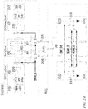
FIG. 2A is a schematic diagram of a display panel and a drive and sense integrated circuit, according to an embodiment of the present disclosure; -
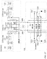
FIG. 2B is a schematic diagram of a display panel and a drive and sense integrated circuit, according to an embodiment of the present disclosure; -
FIG. 2C is a schematic diagram of a display panel and a drive and sense integrated circuit, according to an embodiment of the present disclosure; -
FIG. 3A is a schematic diagram of a front end, according to an embodiment of the present disclosure; -
FIG. 3B is a schematic diagram of a front end, according to an embodiment of the present disclosure; -
FIG. 3C is a schematic diagram of a front end, according to an embodiment of the present disclosure; -
FIG. 4 is a schematic diagram, according to an embodiment of the present disclosure; -
FIG. 5A is a schematic diagram, according to an embodiment of the present disclosure; -
FIG. 5B is a schematic diagram, according to an embodiment of the present disclosure; -
FIG. 5C is a schematic diagram, according to an embodiment of the present disclosure; -
FIG. 5D is a schematic diagram, according to an embodiment of the present disclosure; -
FIG. 5E is a schematic diagram, according to an embodiment of the present disclosure; -
FIG. 5F is a graph of a transfer function, according to an embodiment of the present disclosure; -
FIG. 6 is a flow chart, according to an embodiment of the present disclosure; and -
FIG. 7 is a timing diagram, according to an embodiment of the present disclosure. - The detailed description set forth below in connection with the appended drawings is intended as a description of embodiments of a system and method for sensing drive current in a pixel provided in accordance with the present disclosure and is not intended to represent the only forms in which the present disclosure may be constructed or utilized. The description sets forth the features of the present disclosure in connection with the illustrated embodiments. It is to be understood, however, that the same functions and structures may be accomplished by different embodiments that are also intended to be encompassed within the scope of the disclosure. As denoted elsewhere herein, like element numbers are intended to indicate like elements or features.
- Referring to
FIG. 1 , in some embodiments a display (e.g., a mobile device display) 105 may include a plurality of pixels arranged in rows and columns. Each pixel may be configured to produce light of one color (e.g., red, green or blue) and may be part of a composite pixel that includes, e.g., three such pixels. The composite pixel may be configured to produce any of a wide range of colors (in some contexts, what is referred to herein as a "pixel" is instead referred to as a "sub-pixel", and what is referred to herein as a "composite pixel" is instead referred to as a "pixel"). Each pixel may include a drive circuit, e.g., 7-transistor 1-capacitor (7T1C) drive circuit as shown on the left ofFIG. 1 or a 4-transistor 1-capacitor (4T1C) drive circuit as shown at the bottom ofFIG. 1 . In the 4T1C drive circuit, a drive transistor 110 (the gate-source voltage of which is controlled by the capacitor 115) controls the current through the light emitting diode 120 when the pixel is emitting light. An upperpass-gate transistor 125 may be used to selectively connect the gate of the drive transistor 110 (and one terminal of the capacitor 115) to a power supply voltage. Alower pass-gate transistor 130 may be used to selectively connect adrive sense conductor 135 to a source node 140 (which is a node connected to the source of the drive transistor 110), to the anode of the light emitting diode 120 and to the other terminal of thecapacitor 115. - A pixel drive and sense circuit 145 (discussed in further detail below) may be connected to the
drive sense conductor 135. The pixel drive andsense circuit 145 may include a drive amplifier and a sensing circuit, configured to be selectively connected, one at a time, to thedrive sense conductor 135. When current flows through thedrive transistor 110, and thelower pass-gate transistor 130 is turned-off, disconnecting thedrive sense conductor 135 from the source node 140, current may flow through the light emitting diode 120 causing it to emit light. When thelower pass-gate transistor 130 is turned-on, and thedrive sense conductor 135 is driven to a lower voltage than the cathode of the light emitting diode 120, the light emitting diode 120 may be reverse-biased. Any current flowing in thedrive sense conductor 135 may flow to the pixel drive andsense circuit 145, where the current may be sensed. This sensed current may be compared to a desired current (e.g., the current that an ideal, or nominal transistor would drive at the same gate-source voltage), and to the extent that the sensed current differs from the ideal current, measures may be taken (e.g., the gate-source voltage may be adjusted) to compensate for the discrepancy. - Referring to
FIG. 2A , in some embodiments, the current of any pixel may be sensed in a differential manner, for improved accuracy. For example, if the current driven by thedrive transistor 110 of the pixel on the left ofFIG. 2A (which may be referred to as an "odd" pixel) is to be sensed, it ("odd" pixel) may be turned-on (by charging capacitor of the odd pixel so as to turn on thedrive transistor 110 of the odd pixel). In turn, thedrive transistor 110 of the pixel on the right ofFIG. 2A (which may be referred to as an "even" pixel) may be turned-off (by discharging the capacitor of the even pixel so as to turn off thedrive transistor 110 of the even pixel). The difference between the two corresponding currents flowing out of two respective conductors, which may be referred to as "column conductors" 205, may be measured. Each of thecolumn conductors 205 may be connected to all of the pixels of a column of the display. As a result, even if all of the pixels, other than the odd pixel being characterized, are turned-off, the total leakage current in the other pixels may be significant. To the extent that the leakage currents in the adjacent column (containing the even pixel) are the same, the contribution of the leakage currents to the current flowing in the column conductor connected to the odd pixel may be canceled when the difference between the currents in the twocolumn conductors 205 is sensed. - The SCAN1, SCAN2, and EMIT control lines may be per row, and may have different timing between rows. As mentioned above, differential sensing may be used, so that half the pixels in a row are sensed per operation. The same set of gate control signals may be applied to odd and even pixels, such that there is no distinction between odd and even pixels. Each digital to analog converter and associated
drive amplifier 220 may be used both to drive acolumn conductor 205 to charge the capacitor of a pixel, and to generate the reference current when the current driven by thedrive transistor 110 is being sensed; this may be accomplished using multiplexers, as shown. The embodiment ofFIG. 1 does not include this feature and instead includes two separate digital to analog converters. - Referring to
FIG. 2B , in some embodiments, when the circuit is in drive mode, the gate of thedrive transistor 110 of each pixel is at ELVSS, and the source of thedrive transistor 110 of each pixel is driven to ELVSS - VDRIVE, so that
- The emit transistor of each pixel may remain turned-off.
- In this process, a respective VDRIVE may be stored across the pixel capacitor of each of the pixels. When sensing the odd pixel, the source of the
drive transistor 110 of the even pixel may be driven to ELVSS, so that it (the even pixel) will be turned-off, as mentioned above. - Referring to
FIG. 2C , in some embodiments, when the circuit is in sense mode, the upper pass-gate transistors 125 (FIG. 1 ) are turned-off so that the gates of thedrive transistors 110 float, and so that the charge on the capacitor of each pixel remains constant. The source of thedrive transistor 110 of each pixel is driven (e.g., to VREF, which may be slightly less than ELVSS) so that each light emitting diode 120 is reverse-biased, and so that no current flows through the light emitting diodes 120. The emit transistor of each pixel is turned-on, and as a result of the light emitting diode 120 being reverse-biased, any current driven by thedrive transistor 110 of a pixel flows through arespective column conductor 205 to the sensing circuit. In this mode, the digital to analog converter and thedrive amplifier 220 connected to it may generate the reference current IREF. In some embodiments the reference current is generated by controlling the digital to analog converter and thedrive amplifier 220 to produce a voltage ramp, which is applied to a capacitor to provide a current according to the following equation:
- Various sources of error may be relevant when sensing pixel currents. For example, referring to
FIG. 3A , if current is sensed with a single-ended front end, ground noise Vg may couple into the signal at the output of the amplifier according to the following equation:
- For display systems CP may be much larger than Ci; as a result ground noise (Vg) may be very large at low frequencies.
- Referring to
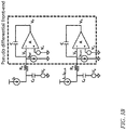
FIG. 3B , pseudo-differential sensing (sensing the difference between an on pixel and an off pixel, as described above, using a pseudo-differential front end) may be effective when the column capacitance (CP) of the two columns matches, but it may be ineffective even with a mismatch of between 1% and 5%. Moreover, the common-mode current caused by the noise may be excessive and may increase the dynamic range requirements of the front end. - Referring to
FIG. 3C , if current is sensed with a single-ended front end, thermal noise Vr may couple into the signal at the output of the amplifier according to the following equation:
- The effect of this wideband thermal noise, which may be generated by the resistance of the column conductor 205 (modeled, in
FIG. 3C , by the resistance RP) may be reduced by using a front end that is configured as, or includes, a low-pass filter, which may pass the (DC) signal (Ipixel) being sensed. An example of such a low-pass filter (an integrator) is shown inFIG. 3C . - In operation, the front-end integrator may be reset prior to the sense operation. Each sense operation may be preceded by a drive operation during which the drive amplifier 220 (
FIGs. 2A-2C ) drives thecolumn conductor 205 to a set voltage. Before a sense operation starts, the voltage on thecolumn conductor 205 may be restored to VREF. Another issue of concern with the circuit ofFIG. 3C may be that because the capacitance to ground of thecolumn conductor 205 may be large, the sense amplifier (in reset mode) may require a long time to bring the voltage of thecolumn conductor 205 to VREF. -
FIG. 4 shows adifferential sensing circuit 400, with two inputs for sensing a difference between a current from a first pixel (e.g., the odd pixel ofFIGs. 2A- 2C ) and a second pixel (e.g., the even pixel ofFIGs. 2A- 2C ) (each current having subtracted from it a respective reference current). The differential sensing circuit has a two-stage architecture with a low-pass current filter 405 (e.g., a first integrator, as shown) as the first stage, and an integrator 410 (e.g., a second integrator, as shown) as the second stage. Theintegrator 410 may be coupled to the low-passcurrent filter 405 by two mirroringcapacitors 425. Each of the low-passcurrent filter 405 and theintegrator 410 may include a fully differential operational amplifier with a capacitor (or "feedback capacitor") in each feedback path. As mentioned above, the circuit may be used to perform differential sensing between two adjacent pixels (e.g. a red pixel and a green pixel of a composite pixel containing three pixels, a red pixel, a green pixel, and a blue pixel, or a green pixel and a blue pixel of a composite pixel). A wideband common mode feedback amplifier 415 (which may have an open loop bandwidth of between 10 MHz and 100 MHz) feeds back around the low-passcurrent filter 405. - For ease of illustration, the circuit of
FIG. 4 shows both thedrive amplifier 220 and thedifferential sensing circuit 400 simultaneously connected to thepixels 420 through respective resistor-capacitor networks used to model thecolumn conductors 205. In some embodiments, however, there is only onecolumn conductor 205 per pixel, and either thedrive amplifier 220 or thedifferential sensing circuit 400 is connected to thecolumn conductor 205 at any time (as shown inFIGs. 2A-2C , in which multiplexers are used to select whether thedrive amplifier 220 or the differential sensing circuit is connected to thecolumn conductor 205 at any time). - In some embodiments, the low-pass
current filter 405 and theintegrator 410 may be fully differential. As used herein, a fully differential circuit is one that (unlike a single-ended or pseudo-differential amplifier) does not compare the signal to ground. Instead, each differential gain stage in a fully differential amplifier, for example, compares the two signals being processed directly to each other. - The wideband common
mode feedback amplifier 415 may compute the common mode output signal at the output of the low-pass current filter 405 (e.g., it may compute the average of the voltages at the two output conductors using a resistor network), and feed back to a common mode input in the low-passcurrent filter 405. The common mode input may be, for example, (i) a gate of a current source (or "tail current source") connected to the two sources of a differential pair in the low-passcurrent filter 405, or (ii) a node connected to two corresponding transistors in the load network of a differential pair in the low-passcurrent filter 405. - In some embodiments, the performance of the circuit of
FIG. 4 may be superior to that of a pseudo-differential circuit (e.g., as illustrated inFIG. 3B ). This may be shown as follows.

- Noting that

and referring to the circuit ofFIG. 5B , it may be found that

-
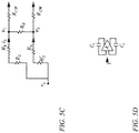
FIG. 5C shows a circuit that may be used to analyze the low-passcurrent filter 405 ofFIG. 4 . In this circuit:

- Referring to
FIG. 5D , it is noted that the differential impedance is

- The following definitions are used:


- From the previous equations:


- Referring to
FIG. 5E , the following may be approximate component values:
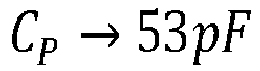


- For f << f 3dB , and using the following assumptions:


- For ft3dB << f << fug
with fug ≡ f 3dB · A


- The resulting transfer function is plotted in
FIG. 5F . At low frequencies, Vout/Vg ≈ ΔCp/Cp. - For frequencies less than f 3dB , the differential impedance looking into the input terminals may be that of a large capacitor Ci * A (the operational amplifier may cause the relatively small capacitor Ci to look much larger, i.e., to make it look like Ci * A). It may be advantageous for this apparent size to be significantly larger than the capacitance of the channel itself, i.e., for the impedance looking into the low-pass current filter to be significantly smaller than the impedance of the channel itself. In this circumstance, the bulk of the current driven by the
drive transistor 110 flows into the low-pass current filter. For frequencies between f 3dB and fug , the differential impedance looking into the input terminals may have the characteristics of a resistor. -
FIG. 6 shows a flow chart of a method for sensing, using the circuits described herein. First, at 605, the odd pixel is driven with the desired Vgs for sensing, and the even pixel is driven with the Vgs corresponding to black (no emission from the light emitting diode 120). Then, at 610, the upperpass-gate transistor 125 of each pixel is turned off, and both pixels are driven with the Vgs corresponding to black, to reset the column conductors 205 (this drive step does not affect the charges on the capacitors of the pixels, because the upperpass-gate transistor 125 of each pixel is turned-off). Then, at 615, the circuit enters sense mode. During this step, the front end is in reset, i.e., switches (e.g., transistor switches) connected across the feedback capacitors of the low-passcurrent filter 405 and theintegrator 410 are closed (e.g., the transistors are turned on) so that these capacitors become, and remain, discharged during the reset. The circuit may stay in reset mode until the sense front-end voltage and the voltage on thecolumn conductors 205 equalize; the effect of this state may be to sample the front end offset. In other words, the reset mode enables thecolumn conductor 205 to equalize with a reference voltage. The pixel current may be turned on or off (i.e., the control signal EMIT_ENB may be either high level or low level) during the reset phase. Then, at 620, the front end is released from reset (e.g., the transistors connected across the feedback capacitors are turned-off), and integration (of the sensed current) begins. Finally, at 625, the output of theintegrator 410 is sampled. The reference voltage (or reference current provided by a current source) is applied to thefirst column conductor 205 during integration. In this way, the effect of residual currents on thecolumn conductor 205 can be reduced. -
FIG. 7 is a timing diagram showing control signals for cycling through the states illustrated inFIG. 6 . The reference symbols ofFIG. 6 are repeated to show the correspondence between the steps ofFIG. 6 and time intervals inFIG. 7 . Further features, not shown inFIG. 7 , may be present in some embodiments. For example, a wait state 705 (in which the low-passcurrent filter 405 is released from reset and allowed to settle, while theintegrator 410 remains in reset mode) may precede the integrating state 620 (which may begin correspondingly later). As another example, in some embodiments, the integrating state is divided into two portions. In one portion, the currents from both the even and odd pixels are turned-off (by turning off the lowerpass-gate transistors 130, using the SCAN2_EN control signal). In the other portion, the even and odd pixels are turned-on (by turning on the lowerpass-gate transistors 130, using the SCAN2_EN control signal). During the transition between the two portions, the polarity of the connection between the low-passcurrent filter 405 and theintegrator 410 may be reversed, so that the output of the integrator, at the end of the second portion, may be the difference between the current when the pixels are on and the current when the pixels are off (the latter of which may include contributions (e.g., leakage currents from other pixels to the extent that their effect is not identical in the even and odd pixels) that are not of interest). As such, operating in this mode may reduce errors due to such currents that are not the current to be sensed (the current driven by thedrive transistor 110 of the odd pixel). Ahold state 710, during which the low-passcurrent filter 405 is disconnected from theintegrator 410 may also be present, to reduce errors that otherwise may be introduced as a result of imperfect timing when the pixel current and reference current are turned on. The SENSE_RESETB and SENSE_INTEG_EN signals may be used to control the reset states of the low-pass filter and integrator respectively. The SENSE_INTEG_EN signal may remain low level until the end of thewait state 705 if a wait state is used. - As used herein, an "input" of a circuit includes one or more conductors and may include further inputs. For example, a differential input may include a first conductor identified as a noninverting input and a second conductor identified as an inverting input. Similarly, an "output" of a circuit, as used herein, includes one or more conductors and may include further outputs. For example, a differential output may include a first conductor identified as a noninverting output and a second conductor identified as an inverting output. As used herein, when a first component is described as being "selectively connected" to a second component, the first component is connected to the second component by a switch (e.g., a transistor switch), so that, depending on the state of the switch, the first component may be connected to the second component or disconnected from the second component.
- Although the present disclosure provides examples of a fully differential circuit in applications in which it is used for sensing a pixel circuit, the present disclosure is not limited to such applications, and systems and methods disclosed herein may be employed in other applications, such as, for example, biomedical applications.
- In some embodiments, the control of various control signals and of circuits like the digital to analog converter may be performed by a processing circuit. The term "processing circuit" is used herein to mean any combination of hardware, firmware, and software, employed to process data or digital signals. Processing circuit hardware may include, for example, application specific integrated circuits (ASICs), general purpose or special purpose central processing units (CPUs), digital signal processors (DSPs), graphics processing units (GPUs), and programmable logic devices such as field programmable gate arrays (FPGAs). In a processing circuit, as used herein, each function is performed either by hardware configured, i.e., hard-wired, to perform that function, or by more general purpose hardware, such as a CPU, configured to execute instructions stored in a non-transitory storage medium. A processing circuit may be fabricated on a single printed circuit board (PCB) or distributed over several interconnected PCBs. A processing circuit may contain other processing circuits; for example a processing circuit may include two processing circuits, an FPGA and a CPU, interconnected on a PCB.
- It will be understood that, although the terms "first", "second", "third", etc., may be used herein to describe various elements, components, regions, layers and/or sections, these elements, components, regions, layers and/or sections should not be limited by these terms. These terms are only used to distinguish one element, component, region, layer or section from another element, component, region, layer or section. Thus, a first element, component, region, layer or section discussed herein could be termed a second element, component, region, layer or section, without departing from the scope of the inventive concept.
- Spatially relative terms, such as "beneath", "below", "lower", "under", "above", "upper" and the like, may be used herein for ease of description to describe one element or feature's relationship to another element(s) or feature(s) as illustrated in the figures. It will be understood that such spatially relative terms are intended to encompass different orientations of the device in use or in operation, in addition to the orientation depicted in the figures. For example, if the device in the figures is turned over, elements described as "below" or "beneath" or "under" other elements or features would then be oriented "above" the other elements or features. Thus, the example terms "below" and "under" can encompass both an orientation of above and below. The device may be otherwise oriented (e.g., rotated 90 degrees or at other orientations) and the spatially relative descriptors used herein should be interpreted accordingly. In addition, it will also be understood that when a layer is referred to as being "between" two layers, it can be the only layer between the two layers, or one or more intervening layers may also be present.
- The terminology used herein is for the purpose of describing particular embodiments only and is not intended to be limiting of the inventive concept. As used herein, the terms "substantially," "about," and similar terms are used as terms of approximation and not as terms of degree, and are intended to account for the inherent deviations in measured or calculated values that would be recognized by those of ordinary skill in the art. As used herein, the term "major portion", when applied to a plurality of items, means at least half of the items.
- As used herein, the singular forms "a" and "an" are intended to include the plural forms as well, unless the context clearly indicates otherwise. It will be further understood that the terms "comprises" and/or "comprising", when used in this specification, specify the presence of stated features, integers, steps, operations, elements, and/or components, but do not preclude the presence or addition of one or more other features, integers, steps, operations, elements, components, and/or groups thereof. As used herein, the term "and/or" includes any and all combinations of one or more of the associated listed items. Expressions such as "at least one of," when preceding a list of elements, modify the entire list of elements and do not modify the individual elements of the list. Further, the use of "may" when describing embodiments of the inventive concept refers to "one or more embodiments of the present disclosure". Also, the term "exemplary" is intended to refer to an example or illustration. As used herein, the terms "use," "using," and "used" may be considered synonymous with the terms "utilize," "utilizing," and "utilized," respectively.
- It will be understood that when an element or layer is referred to as being "on", "connected to", "coupled to", or "adjacent to" another element or layer, it may be directly on, connected to, coupled to, or adjacent to the other element or layer, or one or more intervening elements or layers may be present. In contrast, when an element or layer is referred to as being "directly on", "directly connected to", "directly coupled to", or "immediately adjacent to" another element or layer, there are no intervening elements or layers present.
- Any numerical range recited herein is intended to include all sub-ranges of the same numerical precision subsumed within the recited range. For example, a range of "1.0 to 10.0" is intended to include all subranges between (and including) the recited minimum value of 1.0 and the recited maximum value of 10.0, that is, having a minimum value equal to or greater than 1.0 and a maximum value equal to or less than 10.0, such as, for example, 2.4 to 7.6. Any maximum numerical limitation recited herein is intended to include all lower numerical limitations subsumed therein and any minimum numerical limitation recited in this specification is intended to include all higher numerical limitations subsumed therein.
- Although embodiments of a system and method for sensing drive current in a pixel have been specifically described and illustrated herein, many modifications and variations will be apparent to those skilled in the art. Accordingly, it is to be understood that a system and method for sensing drive current in a pixel constructed according to principles of this disclosure may be embodied other than as specifically described herein. The invention is also defined in the following claims.
Claims (18)
- A system, comprising:a first pixel;a second pixel;a differential sensing circuit;a reference current source; anda control circuit,the differential sensing circuit havinga first input,a second input, andan output,the first input being connected to a node at which a reference current generated by the reference current source is subtracted from a first pixel current, the first pixel current including a current generated by the first pixel;the second input being configured to receive a second pixel current, the second pixel current including a current generated by the second pixel;the output being configured to produce an output signal based on a difference between a current received at the first input and a current received at the second input;the control circuit being configured to:cause the first pixel to be turned on;cause the second pixel to be turned off; andcause the reference current source to generate the reference current.
- The system of claim 1, wherein:the system comprises a display panel comprising the first pixel and the second pixel,the first pixel is in a first column of the display panel,the second pixel is in a second column of the display panel, andthe first pixel and the second pixel are adjacent, and in the same row of the display panel.
- The system of claim 2, wherein:the first pixel current further includes leakage currents from a plurality of pixels in the first column, other than the first pixel, andthe second pixel current includes leakage currents from a plurality of pixels in the second column, other than the second pixel.
- The system of claim 3, wherein the differential sensing circuit comprises a low-pass current filter.
- The system of claim 4, wherein the low-pass current filter comprises a fully differential amplifier.
- The system of claim 5, wherein the low-pass current filter further comprises a common-mode feedback circuit with a bandwidth of at least 1 MHz.
- The system of any of claims 4 to 6, wherein the differential sensing circuit further comprises an integrator, connected to an output of the low-pass current filter.
- The system of claim 7, further comprising a drive circuit,
wherein a first conductor of the display panel is connected to the first pixel, the first conductor being configured:in a first state of the system, to carry the first pixel current, andin a second state of the system, to carry a current from the drive circuit to the first pixel. - The system of claim 8, wherein the control circuit is configured, in the second state:to cause the low-pass current filter to operate in a reset state, andto cause the drive circuit to drive the first conductor to a reference voltage.
- A method for sensing a current in a display, the display comprising:a first pixel;a second pixel;a differential sensing circuit; anda reference current source;the differential sensing circuit havinga first input,a second input, andan output,the method comprising:feeding to the first input the difference between a first pixel current and a reference current generated by the reference current source, the first pixel current including a current generated by the first pixel;feeding to the second input a second pixel current, the second pixel current including a current generated by the second pixel;producing at the output an output signal based on a difference between the current received at the first input and the current received at the second input;turning the first pixel on;turning the second pixel off; andgenerating the reference current.
- The method of claim 10, wherein:the display comprises a display panel comprising the first pixel and the second pixel,the first pixel is in a first column of the display panel,the second pixel is in a second column of the display panel, andthe first pixel and the second pixel are adjacent, and in the same row of the display panel.
- The method of claim 11, wherein:the first pixel current further includes leakage currents from a plurality of pixels in the first column, other than the first pixel, andthe second pixel current includes leakage currents from a plurality of pixels in the second column, other than the second pixel.
- The method of claim 12, wherein the differential sensing circuit comprises a low-pass current filter.
- The method of claim 13, wherein the low-pass current filter comprises a fully differential amplifier.
- The method of claim 14, wherein the low-pass current filter further comprises a common-mode feedback circuit with a bandwidth of at least 1 MHz.
- The method of any of claims 13 to 15, wherein the differential sensing circuit further comprises an integrator, connected to an output of the low-pass current filter.
- The method of claim 16, wherein the display further comprises a drive circuit,
wherein a first conductor of the display panel is connected to the first pixel, the first conductor being configured:in a first state of the display, to carry the first pixel current, andin a second state of the display, to carry a current from the drive circuit to the first pixel. - The method of claim 17, further comprising, in the second state:operating the low-pass current filter in a reset state, anddriving, by the drive circuit, the first conductor to a reference voltage.
Applications Claiming Priority (2)
| Application Number | Priority Date | Filing Date | Title |
|---|---|---|---|
| US201962887395P | 2019-08-15 | 2019-08-15 | |
| US16/656,447 US11087656B2 (en) | 2019-08-15 | 2019-10-17 | Fully differential front end for sensing |
Publications (2)
| Publication Number | Publication Date |
|---|---|
| EP3779949A1 true EP3779949A1 (en) | 2021-02-17 |
| EP3779949B1 EP3779949B1 (en) | 2025-08-06 |
Family
ID=69571825
Family Applications (1)
| Application Number | Title | Priority Date | Filing Date |
|---|---|---|---|
| EP20156633.8A Active EP3779949B1 (en) | 2019-08-15 | 2020-02-11 | Fully differential front end for sensing |
Country Status (6)
| Country | Link |
|---|---|
| US (1) | US11087656B2 (en) |
| EP (1) | EP3779949B1 (en) |
| JP (1) | JP7658722B2 (en) |
| KR (1) | KR102666536B1 (en) |
| CN (1) | CN112447127B (en) |
| TW (1) | TWI839485B (en) |
Families Citing this family (3)
| Publication number | Priority date | Publication date | Assignee | Title |
|---|---|---|---|---|
| US11961468B2 (en) * | 2020-09-22 | 2024-04-16 | Samsung Display Co., Ltd. | Multi-pixel collective adjustment for steady state tracking of parameters |
| TWI779595B (en) * | 2021-05-06 | 2022-10-01 | 瑞昱半導體股份有限公司 | Signal detection circuit |
| US12381527B2 (en) | 2022-02-24 | 2025-08-05 | Samsung Display Co., Ltd. | Continuous time linear equalization (CTLE) feedback for tunable DC gain and mid-band correction |
Citations (2)
| Publication number | Priority date | Publication date | Assignee | Title |
|---|---|---|---|---|
| US20150009204A1 (en) * | 2013-01-14 | 2015-01-08 | Ignis Innovation Inc. | Cleaning common unwanted signals from pixel measurements in emissive displays |
| US20190221146A1 (en) * | 2016-09-21 | 2019-07-18 | Apple Inc. | Noise mitigation for display panel sensing |
Family Cites Families (65)
| Publication number | Priority date | Publication date | Assignee | Title |
|---|---|---|---|---|
| US5239210A (en) * | 1991-01-15 | 1993-08-24 | Crystal Semiconductor, Inc. | Low distortion unity gain amplifier for dac |
| US5969758A (en) | 1997-06-02 | 1999-10-19 | Sarnoff Corporation | DC offset and gain correction for CMOS image sensor |
| US6885396B1 (en) | 1998-03-09 | 2005-04-26 | Micron Technology, Inc. | Readout circuit with gain and analog-to-digital a conversion for image sensor |
| US6275097B1 (en) * | 1999-04-02 | 2001-08-14 | S3 Incorporated, Inc. | Differential charge pump with low voltage common mode feedback circuit |
| US6753913B1 (en) | 1999-09-03 | 2004-06-22 | Texas Instruments Incorporated | CMOS analog front end architecture with variable gain for digital cameras and camcorders |
| US6822679B1 (en) | 2000-10-31 | 2004-11-23 | Texas Instruments Incorporated | Offset correction to the output of a charge coupled device |
| US6538513B2 (en) * | 2000-12-22 | 2003-03-25 | Intersil Americas Inc. | Common mode output current control circuit and method |
| US6753801B2 (en) | 2002-08-23 | 2004-06-22 | Micron Technology, Inc. | Fully differential reference driver for pipeline analog to digital converter |
| US6919551B2 (en) | 2002-08-29 | 2005-07-19 | Micron Technology Inc. | Differential column readout scheme for CMOS APS pixels |
| CA2443206A1 (en) | 2003-09-23 | 2005-03-23 | Ignis Innovation Inc. | Amoled display backplanes - pixel driver circuits, array architecture, and external compensation |
| US20050243193A1 (en) | 2004-04-30 | 2005-11-03 | Bob Gove | Suppression of row-wise noise in an imager |
| EP1594308A1 (en) | 2004-05-07 | 2005-11-09 | Dialog Semiconductor GmbH | Single line Bayer filter RGB bad pixel correction |
| US7230486B2 (en) | 2004-12-23 | 2007-06-12 | Micron Technology, Inc. | Low voltage CMOS differential amplifier |
| KR100670494B1 (en) | 2005-04-26 | 2007-01-16 | 매그나칩 반도체 유한회사 | Driving circuit and driving method of liquid crystal display device |
| JP2007043433A (en) | 2005-08-03 | 2007-02-15 | Renesas Technology Corp | Semiconductor integrated circuit device |
| US8228096B2 (en) | 2007-03-02 | 2012-07-24 | Kawasaki Microelectronics, Inc. | Circuit and method for current-mode output driver with pre-emphasis |
| KR101409514B1 (en) | 2007-06-05 | 2014-06-19 | 엘지디스플레이 주식회사 | Liquid crystal display and driving method thereof |
| JP4508222B2 (en) | 2007-08-31 | 2010-07-21 | ソニー株式会社 | Precharge control method and display device |
| US7667501B2 (en) | 2008-03-19 | 2010-02-23 | Texas Instruments Incorporated | Correlated double sampling technique |
| US7764118B2 (en) | 2008-09-11 | 2010-07-27 | Analog Devices, Inc. | Auto-correction feedback loop for offset and ripple suppression in a chopper-stabilized amplifier |
| US9370075B2 (en) | 2008-12-09 | 2016-06-14 | Ignis Innovation Inc. | System and method for fast compensation programming of pixels in a display |
| US20100271517A1 (en) | 2009-04-24 | 2010-10-28 | Yannick De Wit | In-pixel correlated double sampling pixel |
| US8405747B2 (en) * | 2011-02-17 | 2013-03-26 | Omnivision Technologies, Inc. | Analog row black level calibration for CMOS image sensor |
| EP2715711A4 (en) | 2011-05-28 | 2014-12-24 | Ignis Innovation Inc | System and method for fast compensation programming of pixels in a display |
| US9191598B2 (en) | 2011-08-09 | 2015-11-17 | Altasens, Inc. | Front-end pixel fixed pattern noise correction in imaging arrays having wide dynamic range |
| US20130082936A1 (en) * | 2011-09-29 | 2013-04-04 | Sharp Kabushiki Kaisha | Sensor array with high linearity |
| KR20130053458A (en) | 2011-11-14 | 2013-05-24 | 엘지전자 주식회사 | Display device, method for controlling electric current |
| TW201324261A (en) | 2011-12-01 | 2013-06-16 | Novatek Microelectronics Corp | Multi-touch positioning method |
| US8497731B1 (en) | 2012-05-07 | 2013-07-30 | Freescale Semiconductor, Inc. | Low pass filter circuit |
| MX340482B (en) | 2012-07-11 | 2016-07-08 | Lg Electronics Inc | Method and apparatus for processing video signal. |
| US9305492B2 (en) | 2012-08-02 | 2016-04-05 | Sharp Kabushiki Kaisha | Display device and method for driving the same |
| KR102005052B1 (en) | 2012-12-03 | 2019-07-31 | 삼성디스플레이 주식회사 | Error Compensation part and Organic Light Emitting Display Device Using the same |
| US9171504B2 (en) | 2013-01-14 | 2015-10-27 | Ignis Innovation Inc. | Driving scheme for emissive displays providing compensation for driving transistor variations |
| CN105144274B (en) | 2013-04-23 | 2017-07-11 | 夏普株式会社 | Display device and its driving current detection method |
| CN103354081B (en) * | 2013-07-11 | 2016-04-20 | 京东方科技集团股份有限公司 | Pixel driving current extraction element and pixel driving current extracting method |
| DE102013218973B4 (en) * | 2013-09-20 | 2015-11-19 | Albert-Ludwigs-Universität Freiburg | Method and circuit for time-continuous detection of the position of the sensor mass with simultaneous feedback for capacitive sensors |
| KR102197026B1 (en) | 2014-02-25 | 2020-12-31 | 삼성디스플레이 주식회사 | Organic light emitting display device |
| US9823787B2 (en) | 2014-03-11 | 2017-11-21 | Synaptics Incorporated | Absolute capacitive sensing using sensor electrode pre-emphasis |
| US9722582B2 (en) | 2014-05-21 | 2017-08-01 | SK Hynix Inc. | Semiconductor device with output driver pre-emphasis scheme |
| CN104123911B (en) | 2014-07-01 | 2016-05-04 | 京东方科技集团股份有限公司 | A kind of driving method, drive unit and organic elctroluminescent device |
| KR102221788B1 (en) | 2014-07-14 | 2021-03-02 | 삼성전자주식회사 | Display driver ic for driving with high speed and controlling method thereof |
| TWI540899B (en) * | 2014-08-28 | 2016-07-01 | 原相科技股份有限公司 | Image sensor and operating method thereof |
| KR102261356B1 (en) | 2014-12-09 | 2021-06-04 | 엘지디스플레이 주식회사 | Current sensing circuit and organic light emitting diode display including the same |
| US10191597B2 (en) * | 2015-06-30 | 2019-01-29 | Synaptics Incorporated | Modulating a reference voltage to preform capacitive sensing |
| JP6494335B2 (en) | 2015-03-05 | 2019-04-03 | キヤノン株式会社 | Photoelectric conversion device, photoelectric conversion device driving method, and photoelectric conversion system |
| KR102285393B1 (en) | 2015-03-13 | 2021-08-04 | 삼성디스플레이 주식회사 | Organic light emitting Display and driving method thereof |
| KR20160148831A (en) | 2015-06-16 | 2016-12-27 | 삼성디스플레이 주식회사 | Display device and driving method thereof |
| KR102457754B1 (en) | 2015-08-04 | 2022-10-24 | 삼성디스플레이 주식회사 | Organic light emitting display device and method of driving the same |
| CA2900170A1 (en) | 2015-08-07 | 2017-02-07 | Gholamreza Chaji | Calibration of pixel based on improved reference values |
| US9811205B2 (en) * | 2015-09-29 | 2017-11-07 | Synaptics Incorporated | Variable time anti-aliasing filter |
| KR102427553B1 (en) | 2015-12-01 | 2022-08-02 | 엘지디스플레이 주식회사 | Current integrator and organic light emitting diode display including the same |
| US10762836B1 (en) | 2016-02-18 | 2020-09-01 | Apple Inc. | Electronic display emission scanning using row drivers and microdrivers |
| WO2017214638A1 (en) * | 2016-06-10 | 2017-12-14 | Williams, Jack | System for wireless recording and stimulating of bioelectric events |
| US10393909B2 (en) | 2016-10-11 | 2019-08-27 | Arizona Board Of Regents On Behalf Of The University Of Arizona | Differential target antenna coupling (“DTAC”) data corrections |
| KR102627275B1 (en) | 2016-10-25 | 2024-01-23 | 엘지디스플레이 주식회사 | Organic Light Emitting Display Device |
| KR102617966B1 (en) | 2016-12-28 | 2023-12-28 | 엘지디스플레이 주식회사 | Electroluminescent Display Device and Driving Method thereof |
| US20180336816A1 (en) | 2017-05-19 | 2018-11-22 | Samsung Electronics Co., Ltd. | Display driver circuit for pre-emphasis operation |
| KR102365310B1 (en) | 2017-07-31 | 2022-02-22 | 삼성디스플레이 주식회사 | Display device |
| US10714011B2 (en) * | 2017-09-21 | 2020-07-14 | Apple Inc. | OLED voltage driver with current-voltage compensation |
| JP2020534561A (en) | 2017-09-21 | 2020-11-26 | アップル インコーポレイテッドApple Inc. | OLED voltage driver with current-voltage compensation |
| SG11202010395XA (en) * | 2018-05-02 | 2020-11-27 | Oncosec Medical Inc | Electroporation systems, methods, and apparatus |
| US11012044B2 (en) * | 2018-09-19 | 2021-05-18 | Sensata Technologies, Inc. | Amplifier with common mode detection |
| US10984712B2 (en) | 2018-12-10 | 2021-04-20 | Sharp Kabushiki Kaisha | TFT pixel circuit for OLED external compensation using an adjusted data voltage for component compensation |
| KR102560747B1 (en) | 2018-12-20 | 2023-07-27 | 엘지디스플레이 주식회사 | Organic Light Emitting Display Device And Pixel Sensing Method Of The Same |
| TWI694718B (en) | 2019-01-21 | 2020-05-21 | 友達光電股份有限公司 | Driving apparatus and driving signal generating method thereof |
-
2019
- 2019-10-17 US US16/656,447 patent/US11087656B2/en active Active
-
2020
- 2020-01-06 KR KR1020200001591A patent/KR102666536B1/en active Active
- 2020-02-11 EP EP20156633.8A patent/EP3779949B1/en active Active
- 2020-03-13 TW TW109108306A patent/TWI839485B/en active
- 2020-03-27 JP JP2020058990A patent/JP7658722B2/en active Active
- 2020-05-12 CN CN202010396204.7A patent/CN112447127B/en active Active
Patent Citations (2)
| Publication number | Priority date | Publication date | Assignee | Title |
|---|---|---|---|---|
| US20150009204A1 (en) * | 2013-01-14 | 2015-01-08 | Ignis Innovation Inc. | Cleaning common unwanted signals from pixel measurements in emissive displays |
| US20190221146A1 (en) * | 2016-09-21 | 2019-07-18 | Apple Inc. | Noise mitigation for display panel sensing |
Also Published As
| Publication number | Publication date |
|---|---|
| US11087656B2 (en) | 2021-08-10 |
| EP3779949B1 (en) | 2025-08-06 |
| CN112447127A (en) | 2021-03-05 |
| TW202110279A (en) | 2021-03-01 |
| US20210049943A1 (en) | 2021-02-18 |
| JP7658722B2 (en) | 2025-04-08 |
| JP2021033256A (en) | 2021-03-01 |
| TWI839485B (en) | 2024-04-21 |
| CN112447127B (en) | 2025-07-25 |
| KR102666536B1 (en) | 2024-05-16 |
| KR20210021254A (en) | 2021-02-25 |
Similar Documents
| Publication | Publication Date | Title |
|---|---|---|
| US11069282B2 (en) | Correlated double sampling pixel sensing front end | |
| US10032409B1 (en) | Calibration apparatus for OLED sub-pixel circuit, source electrode driving circuit, and data voltage compensation method | |
| EP3779949B1 (en) | Fully differential front end for sensing | |
| US20140152642A1 (en) | Error compensator and organic light emitting display device using the same | |
| US20050248515A1 (en) | Stabilized active matrix emissive display | |
| EP3779951B1 (en) | Method and system of compensating characteristics of display device | |
| US11081064B1 (en) | Reference signal generation by reusing the driver circuit | |
| US10713995B2 (en) | Output circuit, data line driver, and display device | |
| US7995047B2 (en) | Current driving device | |
| US12155306B2 (en) | Voltage converter and display device including the same | |
| US12196801B2 (en) | Two-domain two-stage sensing front-end circuits and systems | |
| KR20170080331A (en) | Organic light emitting display apparatus | |
| US9642205B2 (en) | Backlight unit with automatic and real time correction of current driving level | |
| CN110164342B (en) | Threshold voltage detection method and device of driving transistor and display device | |
| US11257416B2 (en) | Voltage mode pre-emphasis with floating phase |
Legal Events
| Date | Code | Title | Description |
|---|---|---|---|
| PUAI | Public reference made under article 153(3) epc to a published international application that has entered the european phase |
Free format text: ORIGINAL CODE: 0009012 |
|
| STAA | Information on the status of an ep patent application or granted ep patent |
Free format text: STATUS: REQUEST FOR EXAMINATION WAS MADE |
|
| 17P | Request for examination filed |
Effective date: 20201019 |
|
| AK | Designated contracting states |
Kind code of ref document: A1 Designated state(s): AL AT BE BG CH CY CZ DE DK EE ES FI FR GB GR HR HU IE IS IT LI LT LU LV MC MK MT NL NO PL PT RO RS SE SI SK SM TR |
|
| AX | Request for extension of the european patent |
Extension state: BA ME |
|
| STAA | Information on the status of an ep patent application or granted ep patent |
Free format text: STATUS: EXAMINATION IS IN PROGRESS |
|
| 17Q | First examination report despatched |
Effective date: 20211008 |
|
| 17Q | First examination report despatched |
Effective date: 20211022 |
|
| P01 | Opt-out of the competence of the unified patent court (upc) registered |
Effective date: 20230516 |
|
| GRAP | Despatch of communication of intention to grant a patent |
Free format text: ORIGINAL CODE: EPIDOSNIGR1 |
|
| STAA | Information on the status of an ep patent application or granted ep patent |
Free format text: STATUS: GRANT OF PATENT IS INTENDED |
|
| INTG | Intention to grant announced |
Effective date: 20250303 |
|
| GRAS | Grant fee paid |
Free format text: ORIGINAL CODE: EPIDOSNIGR3 |
|
| GRAA | (expected) grant |
Free format text: ORIGINAL CODE: 0009210 |
|
| STAA | Information on the status of an ep patent application or granted ep patent |
Free format text: STATUS: THE PATENT HAS BEEN GRANTED |
|
| AK | Designated contracting states |
Kind code of ref document: B1 Designated state(s): AL AT BE BG CH CY CZ DE DK EE ES FI FR GB GR HR HU IE IS IT LI LT LU LV MC MK MT NL NO PL PT RO RS SE SI SK SM TR |
|
| REG | Reference to a national code |
Ref country code: GB Ref legal event code: FG4D |
|
| REG | Reference to a national code |
Ref country code: CH Ref legal event code: EP |
|
| REG | Reference to a national code |
Ref country code: IE Ref legal event code: FG4D |
|
| REG | Reference to a national code |
Ref country code: DE Ref legal event code: R096 Ref document number: 602020055791 Country of ref document: DE |
|
| REG | Reference to a national code |
Ref country code: NL Ref legal event code: FP |
|
| PG25 | Lapsed in a contracting state [announced via postgrant information from national office to epo] |
Ref country code: IS Free format text: LAPSE BECAUSE OF FAILURE TO SUBMIT A TRANSLATION OF THE DESCRIPTION OR TO PAY THE FEE WITHIN THE PRESCRIBED TIME-LIMIT Effective date: 20251206 |
|
| PG25 | Lapsed in a contracting state [announced via postgrant information from national office to epo] |
Ref country code: NO Free format text: LAPSE BECAUSE OF FAILURE TO SUBMIT A TRANSLATION OF THE DESCRIPTION OR TO PAY THE FEE WITHIN THE PRESCRIBED TIME-LIMIT Effective date: 20251106 |
|
| REG | Reference to a national code |
Ref country code: LT Ref legal event code: MG9D |
|
| PG25 | Lapsed in a contracting state [announced via postgrant information from national office to epo] |
Ref country code: PT Free format text: LAPSE BECAUSE OF FAILURE TO SUBMIT A TRANSLATION OF THE DESCRIPTION OR TO PAY THE FEE WITHIN THE PRESCRIBED TIME-LIMIT Effective date: 20251209 |
|
| PG25 | Lapsed in a contracting state [announced via postgrant information from national office to epo] |
Ref country code: FI Free format text: LAPSE BECAUSE OF FAILURE TO SUBMIT A TRANSLATION OF THE DESCRIPTION OR TO PAY THE FEE WITHIN THE PRESCRIBED TIME-LIMIT Effective date: 20250806 |
|
| PG25 | Lapsed in a contracting state [announced via postgrant information from national office to epo] |
Ref country code: HR Free format text: LAPSE BECAUSE OF FAILURE TO SUBMIT A TRANSLATION OF THE DESCRIPTION OR TO PAY THE FEE WITHIN THE PRESCRIBED TIME-LIMIT Effective date: 20250806 |
|
| PG25 | Lapsed in a contracting state [announced via postgrant information from national office to epo] |
Ref country code: GR Free format text: LAPSE BECAUSE OF FAILURE TO SUBMIT A TRANSLATION OF THE DESCRIPTION OR TO PAY THE FEE WITHIN THE PRESCRIBED TIME-LIMIT Effective date: 20251107 |
|
| PG25 | Lapsed in a contracting state [announced via postgrant information from national office to epo] |
Ref country code: SE Free format text: LAPSE BECAUSE OF FAILURE TO SUBMIT A TRANSLATION OF THE DESCRIPTION OR TO PAY THE FEE WITHIN THE PRESCRIBED TIME-LIMIT Effective date: 20250806 |
|
| PG25 | Lapsed in a contracting state [announced via postgrant information from national office to epo] |
Ref country code: LV Free format text: LAPSE BECAUSE OF FAILURE TO SUBMIT A TRANSLATION OF THE DESCRIPTION OR TO PAY THE FEE WITHIN THE PRESCRIBED TIME-LIMIT Effective date: 20250806 |
|
| PG25 | Lapsed in a contracting state [announced via postgrant information from national office to epo] |
Ref country code: PL Free format text: LAPSE BECAUSE OF FAILURE TO SUBMIT A TRANSLATION OF THE DESCRIPTION OR TO PAY THE FEE WITHIN THE PRESCRIBED TIME-LIMIT Effective date: 20250806 Ref country code: BG Free format text: LAPSE BECAUSE OF FAILURE TO SUBMIT A TRANSLATION OF THE DESCRIPTION OR TO PAY THE FEE WITHIN THE PRESCRIBED TIME-LIMIT Effective date: 20250806 |
|
| PG25 | Lapsed in a contracting state [announced via postgrant information from national office to epo] |
Ref country code: RS Free format text: LAPSE BECAUSE OF FAILURE TO SUBMIT A TRANSLATION OF THE DESCRIPTION OR TO PAY THE FEE WITHIN THE PRESCRIBED TIME-LIMIT Effective date: 20251106 |
|
| PG25 | Lapsed in a contracting state [announced via postgrant information from national office to epo] |
Ref country code: ES Free format text: LAPSE BECAUSE OF FAILURE TO SUBMIT A TRANSLATION OF THE DESCRIPTION OR TO PAY THE FEE WITHIN THE PRESCRIBED TIME-LIMIT Effective date: 20250806 |
|
| REG | Reference to a national code |
Ref country code: AT Ref legal event code: MK05 Ref document number: 1822901 Country of ref document: AT Kind code of ref document: T Effective date: 20250806 |
|
| PGFP | Annual fee paid to national office [announced via postgrant information from national office to epo] |
Ref country code: NL Payment date: 20260121 Year of fee payment: 7 |
|
| PG25 | Lapsed in a contracting state [announced via postgrant information from national office to epo] |
Ref country code: SM Free format text: LAPSE BECAUSE OF FAILURE TO SUBMIT A TRANSLATION OF THE DESCRIPTION OR TO PAY THE FEE WITHIN THE PRESCRIBED TIME-LIMIT Effective date: 20250806 |
|
| PGFP | Annual fee paid to national office [announced via postgrant information from national office to epo] |
Ref country code: GB Payment date: 20260122 Year of fee payment: 7 |
|
| PG25 | Lapsed in a contracting state [announced via postgrant information from national office to epo] |
Ref country code: DK Free format text: LAPSE BECAUSE OF FAILURE TO SUBMIT A TRANSLATION OF THE DESCRIPTION OR TO PAY THE FEE WITHIN THE PRESCRIBED TIME-LIMIT Effective date: 20250806 |
|
| PGFP | Annual fee paid to national office [announced via postgrant information from national office to epo] |
Ref country code: DE Payment date: 20260120 Year of fee payment: 7 |
|
| PG25 | Lapsed in a contracting state [announced via postgrant information from national office to epo] |
Ref country code: AT Free format text: LAPSE BECAUSE OF FAILURE TO SUBMIT A TRANSLATION OF THE DESCRIPTION OR TO PAY THE FEE WITHIN THE PRESCRIBED TIME-LIMIT Effective date: 20250806 |
|
| PG25 | Lapsed in a contracting state [announced via postgrant information from national office to epo] |
Ref country code: IT Free format text: LAPSE BECAUSE OF FAILURE TO SUBMIT A TRANSLATION OF THE DESCRIPTION OR TO PAY THE FEE WITHIN THE PRESCRIBED TIME-LIMIT Effective date: 20250806 |
|
| PG25 | Lapsed in a contracting state [announced via postgrant information from national office to epo] |
Ref country code: CZ Free format text: LAPSE BECAUSE OF FAILURE TO SUBMIT A TRANSLATION OF THE DESCRIPTION OR TO PAY THE FEE WITHIN THE PRESCRIBED TIME-LIMIT Effective date: 20250806 |
|
| PG25 | Lapsed in a contracting state [announced via postgrant information from national office to epo] |
Ref country code: SK Free format text: LAPSE BECAUSE OF FAILURE TO SUBMIT A TRANSLATION OF THE DESCRIPTION OR TO PAY THE FEE WITHIN THE PRESCRIBED TIME-LIMIT Effective date: 20250806 Ref country code: EE Free format text: LAPSE BECAUSE OF FAILURE TO SUBMIT A TRANSLATION OF THE DESCRIPTION OR TO PAY THE FEE WITHIN THE PRESCRIBED TIME-LIMIT Effective date: 20250806 |