EP3771972A1 - Detection device and control device - Google Patents
Detection device and control device Download PDFInfo
- Publication number
- EP3771972A1 EP3771972A1 EP18912180.9A EP18912180A EP3771972A1 EP 3771972 A1 EP3771972 A1 EP 3771972A1 EP 18912180 A EP18912180 A EP 18912180A EP 3771972 A1 EP3771972 A1 EP 3771972A1
- Authority
- EP
- European Patent Office
- Prior art keywords
- detection
- electrode
- detection electrode
- mode
- state
- Prior art date
- Legal status (The legal status is an assumption and is not a legal conclusion. Google has not performed a legal analysis and makes no representation as to the accuracy of the status listed.)
- Granted
Links
Images



Classifications
-
- H—ELECTRICITY
- H03—ELECTRONIC CIRCUITRY
- H03K—PULSE TECHNIQUE
- H03K17/00—Electronic switching or gating, i.e. not by contact-making and –breaking
- H03K17/94—Electronic switching or gating, i.e. not by contact-making and –breaking characterised by the way in which the control signals are generated
- H03K17/96—Touch switches
- H03K17/962—Capacitive touch switches
-
- H—ELECTRICITY
- H03—ELECTRONIC CIRCUITRY
- H03K—PULSE TECHNIQUE
- H03K17/00—Electronic switching or gating, i.e. not by contact-making and –breaking
- H03K17/94—Electronic switching or gating, i.e. not by contact-making and –breaking characterised by the way in which the control signals are generated
- H03K17/945—Proximity switches
- H03K17/955—Proximity switches using a capacitive detector
-
- H—ELECTRICITY
- H03—ELECTRONIC CIRCUITRY
- H03K—PULSE TECHNIQUE
- H03K17/00—Electronic switching or gating, i.e. not by contact-making and –breaking
- H03K17/94—Electronic switching or gating, i.e. not by contact-making and –breaking characterised by the way in which the control signals are generated
- H03K17/96—Touch switches
- H03K2017/9602—Touch switches characterised by the type or shape of the sensing electrodes
- H03K2017/9604—Touch switches characterised by the type or shape of the sensing electrodes characterised by the number of electrodes
- H03K2017/9613—Touch switches characterised by the type or shape of the sensing electrodes characterised by the number of electrodes using two electrodes per touch switch
-
- H—ELECTRICITY
- H03—ELECTRONIC CIRCUITRY
- H03K—PULSE TECHNIQUE
- H03K2217/00—Indexing scheme related to electronic switching or gating, i.e. not by contact-making or -breaking covered by H03K17/00
- H03K2217/94—Indexing scheme related to electronic switching or gating, i.e. not by contact-making or -breaking covered by H03K17/00 characterised by the way in which the control signal is generated
- H03K2217/94036—Multiple detection, i.e. where different switching signals are generated after operation of the user is detected at different time instants at different locations during the actuation movement by two or more sensors of the same or different kinds
-
- H—ELECTRICITY
- H03—ELECTRONIC CIRCUITRY
- H03K—PULSE TECHNIQUE
- H03K2217/00—Indexing scheme related to electronic switching or gating, i.e. not by contact-making or -breaking covered by H03K17/00
- H03K2217/94—Indexing scheme related to electronic switching or gating, i.e. not by contact-making or -breaking covered by H03K17/00 characterised by the way in which the control signal is generated
- H03K2217/96—Touch switches
- H03K2217/96054—Double function: touch detection combined with detection of a movable element
-
- H—ELECTRICITY
- H03—ELECTRONIC CIRCUITRY
- H03K—PULSE TECHNIQUE
- H03K2217/00—Indexing scheme related to electronic switching or gating, i.e. not by contact-making or -breaking covered by H03K17/00
- H03K2217/94—Indexing scheme related to electronic switching or gating, i.e. not by contact-making or -breaking covered by H03K17/00 characterised by the way in which the control signal is generated
- H03K2217/96—Touch switches
- H03K2217/9607—Capacitive touch switches
- H03K2217/960755—Constructional details of capacitive touch and proximity switches
- H03K2217/960765—Details of shielding arrangements
Definitions
- the present invention relates to a detection device and a control device.
- detection devices detecting a proximity state of a detection target relative to a detection surface based on a change in an electrostatic capacitance of a detection electrode disposed on the detection surface have been used. Furthermore, in such a detection device, a technique of disposing a shield electrode on a back surface of a detection electrode in an overlapping manner has been used.
- PTL 1 discloses a technique in which shield electrodes are disposed on back sides of a plurality of detection electrodes, approach or contact of an object on a front surface is detected based on changes in electrostatic capacitances of the shield electrodes and a position of the object is detected based on changes in electrostatic capacitances of the individual detection electrodes in a display device.
- PTL 2 discloses, in an input device including shield electrodes in lower layers of a plurality of driving electrodes, a technique in which a driving voltage having the same phase as a driving voltage of a corresponding one of the shield electrodes is applied to a selected one of the driving electrodes and a driving voltage having a phase opposite to a phase of the driving voltage of the shield electrode is applied to the other driving electrodes.
- a detection electrode for detecting contact of a detection target on a detection surface (hereinafter referred to as a "contact detection electrode”) and a detection electrode for detecting approach of the detection target to the detection surface (hereinafter referred to as a “proximity detection electrode”) are different from each other, detection capability is optimized.
- a size of the detection device may be increased.
- one of the detection electrodes disposed on an upper side may deteriorate detection capability of the other of the detection electrodes disposed on a lower side. Therefore, in such a detection device including a plurality of detection electrodes having different detection purposes, deterioration of detection capability is to be suppressed while increase in size of the detection device is suppressed.
- a detection device includes an upper detection electrode, a lower detection electrode disposed under the upper detection electrode in an overlapping manner, a proximity state detection unit configured to detect a proximity state of a detection target relative to a detection surface based on a change in at least one of electrostatic capacitances of the upper detection electrode and the lower detection electrode, and a switching unit configured to perform switching between a first state in which the upper detection electrode and the lower detection electrode are insulated from each other and a second state in which the upper detection electrode and the lower detection electrode are short-circuited to each other.
- deterioration in detection capability may be suppressed while increase in size of the detection device is suppressed.
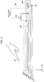
- Fig. 1 is a diagram illustrating a configuration of a detection device 10 according to the embodiment.
- Fig. 2 is a plan view of a detection section 100 included in the detection device 10 according to the embodiment. As illustrated in Figs. 1 and 2 , the detection device 10 includes the detection section 100, a switch 120, and a control circuit 140.
- the detection section 100 is capable of detecting a proximity state of a detection target 20 (such as a finger) relative to a detection surface 10A.
- the detection section 100 has a laminated structure configured by laminating a plurality of components.
- the detection section 100 includes an upper detection electrode 102, an insulation layer 104, a lower detection electrode 106, an insulation layer 107, a shield electrode 108, an insulation layer 110, and a ground electrode 112 in this order from the detection surface 10A (a positive side of a Z axis in Fig. 1 ).
- the upper detection electrode 102 is disposed as an uppermost layer of the detection section 100.
- the lower detection electrode 106 is disposed on a lower side of the upper detection electrode 102 through the insulation layer 104.
- the upper detection electrode 102 and the lower detection electrode 106 detect a proximity state of the detection target 20 relative to the detection surface 10A.
- the upper detection electrode 102 and the lower detection electrode 106 are driven when the control circuit 140 applies alternating voltage.
- an electrostatic capacitance is changed in accordance with a proximity state of the detection target 20
- a current value is changed in accordance with the change in the electrostatic capacitance.
- the current value is detected as a value indicating a proximity state of the detection target 20 by the control circuit 140.
- a thin film conductor such as Indium Tin Oxide (ITO), Indium Zinc Oxide (IZO), or a metallic film (such as silver, copper, and a composite of aluminum and molybdenum), is used.
- ITO Indium Tin Oxide
- IZO Indium Zinc Oxide
- metallic film such as silver, copper, and a composite of aluminum and molybdenum
- the insulation layer 104 is disposed between the upper detection electrode 102 and the lower detection electrode 106 to insulate the upper detection electrode 102 and the lower detection electrode 106 from each other.
- Thin film insulation material may be used as the insulation layer 104.
- an extremely thin resist is applied as the insulation layer 104 in the detection section 100 of this embodiment. By this, the detection section 100 of this embodiment may suppress deterioration of the detection capability of the lower detection electrode 106 using the insulation layer 104.
- the insulation layer 107 is disposed between the lower detection electrode 106 and the shield electrode 108 to insulate the lower detection electrode 106 and the shield electrode 108 from each other. Thin plate insulation material or thin film insulation material may be used as the insulation layer 107.
- the shield electrode 108 is disposed on a lower side of the lower detection electrode 106 through the insulation layer 107.
- the shield electrode driven by the control circuit 140 blocks supply of current from the upper detection electrode 102 and the lower detection electrode 106 to the ground electrode 112 so that electrostatic capacitances detectable by the upper detection electrode 102 and the lower detection electrode 106 are increased.
- a thin plate conductor or a thin film conductor may be used as the shield electrode 108.
- the insulation layer 110 is disposed between the shield electrode 108 and the ground electrode 112 so as to insulate the shield electrode 108 and the ground electrode 112 from each other. Thin plate insulation material or thin film insulation material may be used as the insulation layer 110.
- the ground electrode 112 is disposed as a lowermost layer of the detection section 100.
- the ground electrode 112 is grounded.
- a thin plate conductor or a thin film conductor may be used as the ground electrode 112.
- the switch 120 is electrically connected to the upper detection electrode 102 and the lower detection electrode 106.
- the switch 120 is turned on by a switching signal supplied from the control circuit 140 so that a second state in which the upper detection electrode 102 and the lower detection electrode 106 are short-circuited to each other may be entered.
- the switch 120 is turned off by a switching signal supplied from the control circuit 140 so that a first state in which the upper detection electrode 102 and the lower detection electrode 106 are insulated from each other may be entered.
- the control circuit 140 is an example of a "control device".
- the control circuit 140 is electrically connected to the upper detection electrode 102, the lower detection electrode 106, and the shield electrode 108.
- the control circuit 140 may detect a proximity state of the detection target 20 relative to the detection surface 10A based on a change in an electrostatic capacitance of at least one of the upper detection electrode 102 and the lower detection electrode 106.
- the control circuit 140 controls the switch 120 so as to perform switching between the first state in which the upper detection electrode 102 and the lower detection electrode 106 are insulated from each other and the second state in which the upper detection electrode 102 and the lower detection electrode 106 are short-circuited to each other.
- control circuit 140 may selectively perform switching among a driving state, an open state (non-driving state), and a state of short-circuit with the shield electrode 108 for each of the upper detection electrode 102 and the lower detection electrode 106.
- An integrated circuit (IC), for example, is used as the control circuit 140.
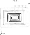
- Fig. 2 is a plan view of a detection section 100 included in the detection device 10 according to the embodiment.
- the lower detection electrode 106 has a detection area larger than that of the upper detection electrode 102 and includes a detection range of the upper detection electrode 102. Specifically, a portion of a detection surface of the lower detection electrode 106 is covered by the upper detection electrode 102.
- the detection section 100 includes a spiral band conductor as the upper detection electrode 102 in the example of Fig. 2
- the number of upper detection electrodes 102 and a shape of the upper detection electrode 102 are not limited to these.
- a plurality of rectangle conductors may be disposed as the upper detection electrode 102 on the detection section 100 in the same plane similarly to the lower detection electrode 106.
- the detection section 100 may have a configuration the same as that of a touch panel employing an electrostatic capacitance method (such as a configuration in which a plurality of detection electrodes are arranged in a matrix), for example, so as to detect a contact position of the detection target 20 on the detection surface 10A.
- a single rectangle conductor is disposed as the lower detection electrode 106 in the detection section 100
- the number of lower detection electrodes 106 and a shape of the lower detection electrode 106 are not limited to these.
- a plurality of conductors may be disposed as the lower detection electrodes 106 on the same plane.
- Fig. 3 is a block diagram illustrating a functional configuration of the control circuit 140 according to the embodiment.
- the control circuit 140 includes an electrode driving section 142, a proximity state detection section 144, a detection signal conversion section 146, an output section 150, and a switching section 152.
- the electrode driving section 142 drives the upper detection electrode 102, the lower detection electrode 106, and the shield electrode 108. Specifically, the electrode driving section 142 drives at least one of the upper detection electrode 102 and the lower detection electrode 106 in accordance with a detection mode of the control circuit 140 and further drives the shield electrode 108. Note that electrodes to be driven by the electrode driving section 142 will be described hereinafter with reference to Fig. 4 for each detection mode. Furthermore, the electrode driving section 142 drives the shield electrode 108 by a driving voltage having the same phase as driving voltages of the upper detection electrode 102 and the lower detection electrode 106.
- the proximity state detection section 144 is an example of a "proximity state detection unit".
- the proximity state detection section 144 detects a current value of an electrode driven by the electrode driving section 142 as a value indicating a proximity state of the detection target 20.
- the proximity state detection section 144 detects a current value of an electrode driven by the electrode driving section 142 (at least one of the upper detection electrode 102 and the lower detection electrode 106) in accordance with a detection mode of the control circuit 140. Note that, when the proximity state of the detection target 20 is changed, an electrostatic capacitance of the electrode driven by the electrode driving section 142 is changed, and accordingly, the current value is changed. Therefore, the current value detected by the proximity state detection section 144 indicates a proximity state of the detection target 20.
- the detection signal conversion section 146 performs a predetermined conversion process on a current value (analog signal) detected by the proximity state detection section 144. For example, the detection signal conversion section 146 performs an analog/digital conversion process on a current value detected by the proximity state detection section 144 as the predetermined conversion process. Note that the detection signal conversion section 146 may perform a process of converting a current value detected by the proximity state detection section 144 into a value of another unit indicating a proximity state of the detection target 20 (such as a proximity distance).
- the output section 150 outputs a current value detected by the proximity state detection section 144 (a current value subjected to the conversion process performed by the detection signal conversion section 146) to an external information processing apparatus as a value indicating a proximity state of the detection target 20.
- the output section 150 may output a detection mode of the control circuit 140 when the current value is detected, in addition to the current value detected by the proximity state detection section 144, to the external information processing apparatus.
- the external information processing apparatus may perform a process corresponding to a detection mode of the control circuit 140, for example.
- the switching section 152 is an example of a "switching unit".
- the switching section 152 switches a detection mode of the control circuit 140 based on a current value detected by the proximity state detection section 144 (that is, an electrostatic capacitance value of an electrode driven by the electrode driving section 142). Specifically, the switching section 152 may change the detection mode of the control circuit 140 in accordance with the proximity state of the detection target 20 on the detection surface 10A.
- the switching section 152 changes the detection mode of the control circuit 140 into a "second distance detection mode" (an example of a "second detection mode") described below.
- the switching section 152 may perform switching to the "second distance detection mode" when the detection target 20 is positioned far away from the detection surface 10A by a predetermined distance in the "proximity detection mode".
- a preferred value corresponding to a detection distance for the switching of a detection mode is stored in a memory in advance as the first threshold value th1, for example.
- the first threshold value th1 may be changed by the external information processing apparatus, for example.
- the switching section 152 switches the detection mode of the control circuit 140 into the "proximity detection mode".
- a preferred value corresponding to a detection distance for the switching of a detection mode is stored in the memory in advance as the second threshold value th2, for example.
- the second threshold value th2 may be changed by the external information processing apparatus, for example.
- the second threshold value th2 may be the same as the first threshold value th1 or may be different from the first threshold value th1.
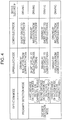
- Fig. 4 is a diagram illustrating a detection mode of the control circuit 140 according to the embodiment. As illustrated in Fig. 4 , the control circuit 140 has the "proximity detection mode” and the “distance detection mode” as the detection modes.
- the “proximity detection mode” is an example of a “first detection mode”.
- the “proximity detection mode” is preferably used to detect the detection target 20 when the detection target 20 is positioned relatively close to the detection surface 10A.
- the “proximity detection mode” is preferably used to detect contact of the detection target 20 on the detection surface 10A.
- the upper detection electrode 102 and the shield electrode 108 are driven in a state in which the upper detection electrode 102 and the lower detection electrode 106 are insulated from each other, and a proximity state of the detection target 20 is detected based on a change in an electrostatic capacitance of the upper detection electrode 102.
- the lower detection electrode 106 is short-circuited to the shield electrode 108 under control of the control circuit 140 in the "proximity detection mode".
- the lower detection electrode 106 may function as a portion of the shield electrode 108 so that capability of blocking of flow of current from the upper detection electrode 102 to the ground electrode 112 may be enhanced.
- the “distance detection mode” is preferably used to detect the detection target 20 when the detection target 20 is positioned relatively far from the detection surface 10A.
- the “distance detection mode” is preferably used to detect a noncontact operation (such as a gesture operation) of the detection target 20 on the detection surface 10A.
- the “distance detection mode” include a “first distance detection mode”, the “second distance detection mode”, and a “third distance detection mode”.
- the “first distance detection mode” is an example of a “fourth detection mode”.
- the “first distance detection mode” has “middle” detection capability.
- the lower detection electrode 106 and the shield electrode 108 are driven in a state in which the upper detection electrode 102 and the lower detection electrode 106 are insulated from each other and the upper detection electrode 102 is short-circuited to the shield electrode 108 (or an open state), and a proximity state of the detection target 20 is detected based on a change in the electrostatic capacitance of the lower detection electrode 106.
- the “second distance mode” is an example of a “second detection mode”.
- the “second distance detection mode” has “large” detection capability.
- the upper detection electrode 102, the lower detection electrode 106, and the shield electrode 108 are driven in a state in which the upper detection electrode 102 and the lower detection electrode 106 are short-circuited to each other, and a proximity state of the detection target 20 is detected based on a change in an electrostatic capacitance of the upper detection electrode 102 and the lower detection electrode 106 which are short-circuited to each other.
- the “third distance detection mode” is an example of a “third detection mode”.
- the “third distance detection mode” has “large” detection capability.
- the upper detection electrode 102, the lower detection electrode 106, and the shield electrode 108 are driven in a state in which the upper detection electrode 102 and the lower detection electrode 106 are insulated from each other, and a proximity state of the detection target 20 is detected based on a change in an electrostatic capacitance of the upper detection electrode 102 and a change in an electrostatic capacitance of the lower detection electrode 106.
- the detection section 100 of this embodiment since the upper detection electrode 102 overlaps on the lower detection electrode 106, a detection area of the lower detection electrode 106 is reduced due to an area of the upper detection electrode 102, and therefore, detection capability of the lower detection electrode 106 may be deteriorated. Therefore, the detection section 100 of this embodiment uses the electrostatic capacitance value of the upper detection electrode 102 in addition to the electrostatic capacitance value of the lower detection electrode 106 in the "second distance detection mode" and the "third distance detection mode", so that the deterioration of the detection capability described above may be compensated for by the electrostatic capacitance value of the upper detection electrode 102.
- a proximity state of the detection target 20 may be detected as if the upper detection electrode 102 does not overlap on the lower detection electrode 106. Accordingly, the detection section 100 of this embodiment may detect a proximity state of the detection target 20 with high accuracy even when the detection target 20 is positioned relatively far from the detection surface 10A.
- a proximity state of the detection target 20 is detected by combining the upper detection electrode 102 and the lower detection electrode 106 in terms of hardware.
- a circuit configuration in which the upper detection electrode 102 and the lower detection electrode 106 are combined in terms of hardware (such as the switch 120) is disposed in the detection device 10.
- the electrode driving section 142 drives the upper detection electrode 102 and the lower detection electrode 106 which are short-circuited to each other as a single detection electrode.
- the proximity state detection section 144 detects a current value of the single detection electrode detected by the proximity state detection section 144 as a value indicating a proximity state of the detection target 20.
- the "third distance detection mode” detects a proximity state of the detection target 20 by combining the electrostatic capacitance value of the upper detection electrode 102 and the electrostatic capacitance value of the lower detection electrode 106 in terms of software.
- a processing program of combining an electrostatic capacitance value of the upper detection electrode 102 and an electrostatic capacitance value of the lower detection electrode 106 is installed in the control circuit 140.
- the electrode driving section 142 drives both the upper detection electrode 102 and the lower detection electrode 106.
- the proximity state detection section 144 calculates a total value of a current value of the upper detection electrode 102 and a current value of the lower detection electrode 106 as a value indicating a proximity state of the detection target 20.
- the "second distance detection mode” or the “third distance detection mode” may be usable in accordance with a use purpose, cost restriction, size restriction, or the like.
- both the “second distance detection mode” and the “third distance detection mode” may be available and the user may arbitrarily select one of the modes.
- both the “second distance detection mode” and the “third distance detection mode” may be available and the “second distance detection mode” and the “third distance detection mode” may be dynamically switched from one to another in accordance with a processing program based on a predetermined switching condition.
- the "first distance detection mode” has detection capability lower than those of the "second distance detection mode” and the “third distance detection mode”
- the “first distance detection mode” is provided in addition to the “second distance detection mode” and the “third distance detection mode” since power consumption of the "first distance detection mode” is smaller than those of the "second distance detection mode” and the “third distance detection mode” and the user may arbitrarily select one of the modes.
- Fig. 5 is a flowchart of a procedure of a process performed by the control circuit 140 according to the embodiment. Note that, although the "second distance detection mode" is used as the “distance detection mode” in this embodiment, other detection modes may be used.
- the switching section 152 switches a detection mode of the control circuit 140 into the "distance detection mode" (step S501). Specifically, the switching section 152 turns on the switch 120 so that the upper detection electrode 102 and the lower detection electrode 106 are short-circuited to each other.
- the electrode driving section 142 drives the upper detection electrode 102 and the lower detection electrode 106 which are short-circuited to each other (step S502).
- the proximity state detection section 144 detects a current value indicating a proximity state of the detection target 20 relative to the detection surface 10A as a change in an electrostatic capacitance of the upper detection electrode 102 and the lower detection electrode 106 driven in step S502 (step S503).
- the detection signal conversion section 146 performs a predetermined conversion process on the current value detected in step S503 (step S504).
- the output section 150 outputs the current value detected in step S503 to the external information processing apparatus (step S505).
- the switching section 152 determines whether the current value detected in step S503 is larger than the predetermined second threshold value th2 (step S506).
- step S506 When it is determined that the current value detected in step S503 is not larger than the predetermined second threshold value th2 in step S506 (step S506: No), the control circuit 140 returns to step S502.
- step S506 when it is determined that the current value detected in step S503 is larger than the predetermined second threshold value th2 in step S506 (step S506: Yes), the switching section 152 switches the detection mode of the control circuit 140 into the "proximity detection mode" (step S507). Specifically, the switching section 152 turns off the switch 120 so that the upper detection electrode 102 and the lower detection electrode 106 are insulated from each other.
- the electrode driving section 142 drives the upper detection electrode 102 (step S508).
- the proximity state detection section 144 detects a current value indicating a proximity state of the detection target 20 relative to the detection surface 10A as a change in an electrostatic capacitance of the upper detection electrode 102 driven in step S509 (step S509).
- the detection signal conversion section 146 performs a predetermined conversion process on the current value detected in step S509 (step S510).
- the output section 150 outputs the current value detected in step S509 to the external information processing apparatus (step S511).
- the switching section 152 determines whether the current value detected in step S509 is smaller than the predetermined first threshold value th1 (step S512).
- step S512 When it is determined that the current value detected in step S510 is not smaller than the predetermined first threshold value th1 in step S512 (step S512: No), the control circuit 140 returns to step S508.
- step S512 Yes
- the control circuit 140 returns to step S501.
- the operation mode of the control circuit 140 is alternately switched between the "distance detection mode” and the "proximity detection mode” in accordance with the proximity state of the detection target 20.
- Fig. 6 is a diagram illustrating a method for correcting a current value employed in the control circuit 140 according to the embodiment.
- a plane configuration of the detection section 100 is illustrated. Note that the insulation layer 104, the insulation layer 107, the insulation layer 110, and the ground electrode 112 are omitted in Fig. 6 for simplicity of the description.
- the numbers of the upper detection electrodes 102 and the lower detection electrodes 106 and shapes of the upper detection electrode 102 and the lower detection electrode 106 are different from those of Fig. 2 .
- a plurality of rectangle lower detection electrodes 106 are arranged in a matrix such that the lower detection electrodes 106 overlap on the shield electrode 108. Furthermore, a plurality of rectangle upper detection electrodes 102 are arranged in a matrix on the plurality of lower detection electrode 106 such that the upper detection electrodes 102 overlap on the lower detection electrodes 106.
- a contact position of the detection target 20 relative to the detection surface 10A is detected in accordance with changes in electrostatic capacitances of the plurality of upper detection electrodes 102 in the "proximity detection mode" described above. Furthermore, in the example of Fig. 6 , a distance of the detection target 20 from the detection surface 10A is detected by changes in electrostatic capacitances of the plurality of upper detection electrodes 102 and the plurality of lower detection electrodes 106 which are short-circuited to each other in the "second distance detection mode" described above.
- a current value in the "second distance detection mode" (that is, a current value of the upper detection electrode 102 and the lower detection electrode 106 which are short-circuited to each other) is ideally equal to a current value of the single lower detection electrode 106 (that is, the upper detection electrode 102 does not overlap on the lower detection electrode 106).
- control circuit 140 may correct the current value of the upper detection electrode 102 and the lower detection electrode 106 which are short-circuited to each other in the "second distance detection mode" to an ideal value.
- a correction coefficient is "1.25". In this case, correction is performed such that the measurement value 2 becomes “100” using the correction coefficient "1.25".
- the control circuit 140 multiplies a current value detected by the proximity state detection section 144 by the correction coefficient "1.25". By this, the current value may be corrected to an ideal value.
- control circuit 140 multiplies a setting value of detection sensitivity of the upper detection electrode 102 and the lower detection electrode 106 by the correction coefficient "1.25". By this, the current value detected by the proximity state detection section 144 may be corrected to an ideal value.
- the detection device 10 includes the upper detection electrode 102, the lower detection electrode 106 disposed under the upper detection electrode 102 in an overlapping manner, the proximity state detection section 144 detecting a proximity state of the detection target 20 relative to the detection surface 10A based on at least one of changes in electrostatic capacitances of the upper detection electrode 102 and the lower detection electrode 106, and the switching section 152 capable of performing switching between the first state in which the upper detection electrode 102 and the lower detection electrode 106 are insulated from each other and the second state in which the upper detection electrode 102 and the lower detection electrode 106 are short-circuited to each other.
- the detection device 10 of this embodiment may compensate for reduction of the detection area of the lower detection electrode 106 using the upper detection electrode 102 by short-circuiting the upper detection electrode 102 and the lower detection electrode 106 to each other.
- increase in size of the detection device 10 may be suppressed since the upper detection electrode 102 and the lower detection electrode 106 are disposed in an overlapping manner. Therefore, according to the detection device 10 of this embodiment, detection capability of the detection device 10 of this embodiment including different detection electrodes of different detection purposes may be suppressed while increase in size of the detection device 10 is suppressed.
- control circuit 140 may be included in the external information processing apparatus installed outside the control circuit 140.
- the upper detection electrode 102 and the lower detection electrode 106 are short-circuited to each other by the switch 120 disposed outside the control circuit 140, a similar switch may be incorporated in the control circuit 140 so as to cause the upper detection electrode 102 and the lower detection electrode 106 to be short-circuited to each other using the switch.
- control circuit 140 may further include a determination section determining a proximity state of the detection target 20 relative to the detection surface 10A based on a current value detected by the proximity state detection section 144.
- the determination section may determine whether the detection target 20 has approached the detection surface 10A based on a current value detected by the proximity state detection section 144. In this case, the determination section may determine whether the detection target 20 has approached the detection surface 10A based on a current value detected by the proximity state detection section 144 and a predetermined threshold value.
- the determination section may determine a proximity distance of the detection target 20 relative to the detection surface 10A based on a current value detected by the proximity state detection section 144. In this case, the determination section may determine a proximity distance of the detection target 20 relative to the detection surface 10A based on a current value detected by the proximity state detection section 144 and a predetermined conversion equation or a predetermined conversion table.
- the output section 150 may output a result of the determination performed by the determination section to the external information processing apparatus.
Landscapes
- Electronic Switches (AREA)
- Geophysics And Detection Of Objects (AREA)
- Measurement Of Length, Angles, Or The Like Using Electric Or Magnetic Means (AREA)
- Switches That Are Operated By Magnetic Or Electric Fields (AREA)
Abstract
Description
- The present invention relates to a detection device and a control device.
- In general, detection devices detecting a proximity state of a detection target relative to a detection surface based on a change in an electrostatic capacitance of a detection electrode disposed on the detection surface have been used. Furthermore, in such a detection device, a technique of disposing a shield electrode on a back surface of a detection electrode in an overlapping manner has been used.
- For example, PTL 1 discloses a technique in which shield electrodes are disposed on back sides of a plurality of detection electrodes, approach or contact of an object on a front surface is detected based on changes in electrostatic capacitances of the shield electrodes and a position of the object is detected based on changes in electrostatic capacitances of the individual detection electrodes in a display device.
- Furthermore, PTL 2 discloses, in an input device including shield electrodes in lower layers of a plurality of driving electrodes, a technique in which a driving voltage having the same phase as a driving voltage of a corresponding one of the shield electrodes is applied to a selected one of the driving electrodes and a driving voltage having a phase opposite to a phase of the driving voltage of the shield electrode is applied to the other driving electrodes.
-
- PTL 1: Japanese Unexamined Patent Application Publication No.
2017-102811 - PTL 2: Japanese Unexamined Patent Application Publication No.
2015-121958 - Here, in the general detection devices, since a detection electrode for detecting contact of a detection target on a detection surface (hereinafter referred to as a "contact detection electrode") and a detection electrode for detecting approach of the detection target to the detection surface (hereinafter referred to as a "proximity detection electrode") are different from each other, detection capability is optimized. However, in the general technique, when the contact detection electrode and the proximity detection electrode are disposed in different positions on the same plane, a size of the detection device may be increased. Furthermore, in the general method, when the contact detection element and the proximity detection element overlap with each other, one of the detection electrodes disposed on an upper side may deteriorate detection capability of the other of the detection electrodes disposed on a lower side. Therefore, in such a detection device including a plurality of detection electrodes having different detection purposes, deterioration of detection capability is to be suppressed while increase in size of the detection device is suppressed.
- A detection device according to an embodiment includes an upper detection electrode, a lower detection electrode disposed under the upper detection electrode in an overlapping manner, a proximity state detection unit configured to detect a proximity state of a detection target relative to a detection surface based on a change in at least one of electrostatic capacitances of the upper detection electrode and the lower detection electrode, and a switching unit configured to perform switching between a first state in which the upper detection electrode and the lower detection electrode are insulated from each other and a second state in which the upper detection electrode and the lower detection electrode are short-circuited to each other.
- According to the present invention, in a detection device including a plurality of detection electrodes having different detection purposes, deterioration in detection capability may be suppressed while increase in size of the detection device is suppressed.
-
- [
Fig. 1] Fig. 1 is a diagram illustrating a configuration of a detection device according to an embodiment. - [
Fig. 2] Fig. 2 is a plan view of a detection section included in the detection device according to the embodiment. - [
Fig. 3] Fig. 3 is a block diagram illustrating a functional configuration of a control circuit according to the embodiment. - [
Fig. 4] Fig. 4 is a diagram illustrating detection modes of the control circuit according to the embodiment. - [
Fig. 5] Fig. 5 is a flowchart of a procedure of a process performed by the control circuit according to the embodiment. - [
Fig. 6] Fig. 6 is a diagram illustrating a method for correcting detection sensitivity of the control circuit according to the embodiment. - Hereinafter, an embodiment will be described with reference to the accompanying drawings.
-
Fig. 1 is a diagram illustrating a configuration of adetection device 10 according to the embodiment.Fig. 2 is a plan view of adetection section 100 included in thedetection device 10 according to the embodiment. As illustrated inFigs. 1 and2 , thedetection device 10 includes thedetection section 100, aswitch 120, and acontrol circuit 140. - The
detection section 100 is capable of detecting a proximity state of a detection target 20 (such as a finger) relative to adetection surface 10A. As illustrated inFigs. 1 and2 , thedetection section 100 has a laminated structure configured by laminating a plurality of components. Specifically, thedetection section 100 includes anupper detection electrode 102, aninsulation layer 104, alower detection electrode 106, aninsulation layer 107, ashield electrode 108, aninsulation layer 110, and aground electrode 112 in this order from thedetection surface 10A (a positive side of a Z axis inFig. 1 ). - The
upper detection electrode 102 is disposed as an uppermost layer of thedetection section 100. Thelower detection electrode 106 is disposed on a lower side of theupper detection electrode 102 through theinsulation layer 104. Theupper detection electrode 102 and thelower detection electrode 106 detect a proximity state of thedetection target 20 relative to thedetection surface 10A. Specifically, theupper detection electrode 102 and thelower detection electrode 106 are driven when thecontrol circuit 140 applies alternating voltage. When an electrostatic capacitance is changed in accordance with a proximity state of thedetection target 20, a current value is changed in accordance with the change in the electrostatic capacitance. The current value is detected as a value indicating a proximity state of thedetection target 20 by thecontrol circuit 140. As theupper detection electrode 102 and thelower detection electrode 106, a thin film conductor, such as Indium Tin Oxide (ITO), Indium Zinc Oxide (IZO), or a metallic film (such as silver, copper, and a composite of aluminum and molybdenum), is used. - The
insulation layer 104 is disposed between theupper detection electrode 102 and thelower detection electrode 106 to insulate theupper detection electrode 102 and thelower detection electrode 106 from each other. Thin film insulation material may be used as theinsulation layer 104. For example, an extremely thin resist is applied as theinsulation layer 104 in thedetection section 100 of this embodiment. By this, thedetection section 100 of this embodiment may suppress deterioration of the detection capability of thelower detection electrode 106 using theinsulation layer 104. - The
insulation layer 107 is disposed between thelower detection electrode 106 and theshield electrode 108 to insulate thelower detection electrode 106 and theshield electrode 108 from each other. Thin plate insulation material or thin film insulation material may be used as theinsulation layer 107. - The
shield electrode 108 is disposed on a lower side of thelower detection electrode 106 through theinsulation layer 107. The shield electrode driven by thecontrol circuit 140 blocks supply of current from theupper detection electrode 102 and thelower detection electrode 106 to theground electrode 112 so that electrostatic capacitances detectable by theupper detection electrode 102 and thelower detection electrode 106 are increased. A thin plate conductor or a thin film conductor may be used as theshield electrode 108. - The
insulation layer 110 is disposed between theshield electrode 108 and theground electrode 112 so as to insulate theshield electrode 108 and theground electrode 112 from each other. Thin plate insulation material or thin film insulation material may be used as theinsulation layer 110. - The
ground electrode 112 is disposed as a lowermost layer of thedetection section 100. Theground electrode 112 is grounded. A thin plate conductor or a thin film conductor may be used as theground electrode 112. - The
switch 120 is electrically connected to theupper detection electrode 102 and thelower detection electrode 106. Theswitch 120 is turned on by a switching signal supplied from thecontrol circuit 140 so that a second state in which theupper detection electrode 102 and thelower detection electrode 106 are short-circuited to each other may be entered. On the other hand, theswitch 120 is turned off by a switching signal supplied from thecontrol circuit 140 so that a first state in which theupper detection electrode 102 and thelower detection electrode 106 are insulated from each other may be entered. - The
control circuit 140 is an example of a "control device". Thecontrol circuit 140 is electrically connected to theupper detection electrode 102, thelower detection electrode 106, and theshield electrode 108. Thecontrol circuit 140 may detect a proximity state of thedetection target 20 relative to thedetection surface 10A based on a change in an electrostatic capacitance of at least one of theupper detection electrode 102 and thelower detection electrode 106. Furthermore, thecontrol circuit 140 controls theswitch 120 so as to perform switching between the first state in which theupper detection electrode 102 and thelower detection electrode 106 are insulated from each other and the second state in which theupper detection electrode 102 and thelower detection electrode 106 are short-circuited to each other. Furthermore, thecontrol circuit 140 may selectively perform switching among a driving state, an open state (non-driving state), and a state of short-circuit with theshield electrode 108 for each of theupper detection electrode 102 and thelower detection electrode 106. An integrated circuit (IC), for example, is used as thecontrol circuit 140. -
Fig. 2 is a plan view of adetection section 100 included in thedetection device 10 according to the embodiment. As illustrated inFig. 2 , in a plan view from the above (the positive direction of the Z axis inFig. 2 ), thelower detection electrode 106 has a detection area larger than that of theupper detection electrode 102 and includes a detection range of theupper detection electrode 102. Specifically, a portion of a detection surface of thelower detection electrode 106 is covered by theupper detection electrode 102. - Although the
detection section 100 includes a spiral band conductor as theupper detection electrode 102 in the example ofFig. 2 , the number ofupper detection electrodes 102 and a shape of theupper detection electrode 102 are not limited to these. For example, a plurality of rectangle conductors may be disposed as theupper detection electrode 102 on thedetection section 100 in the same plane similarly to thelower detection electrode 106. Furthermore, thedetection section 100 may have a configuration the same as that of a touch panel employing an electrostatic capacitance method (such as a configuration in which a plurality of detection electrodes are arranged in a matrix), for example, so as to detect a contact position of thedetection target 20 on thedetection surface 10A. - Furthermore, in the example of
Fig. 2 , although a single rectangle conductor is disposed as thelower detection electrode 106 in thedetection section 100, the number oflower detection electrodes 106 and a shape of thelower detection electrode 106 are not limited to these. For example, in thedetection section 100, a plurality of conductors may be disposed as thelower detection electrodes 106 on the same plane. -
Fig. 3 is a block diagram illustrating a functional configuration of thecontrol circuit 140 according to the embodiment. As illustrated inFig. 3 , thecontrol circuit 140 includes anelectrode driving section 142, a proximity state detection section 144, a detectionsignal conversion section 146, anoutput section 150, and aswitching section 152. - The
electrode driving section 142 drives theupper detection electrode 102, thelower detection electrode 106, and theshield electrode 108. Specifically, theelectrode driving section 142 drives at least one of theupper detection electrode 102 and thelower detection electrode 106 in accordance with a detection mode of thecontrol circuit 140 and further drives theshield electrode 108. Note that electrodes to be driven by theelectrode driving section 142 will be described hereinafter with reference toFig. 4 for each detection mode. Furthermore, theelectrode driving section 142 drives theshield electrode 108 by a driving voltage having the same phase as driving voltages of theupper detection electrode 102 and thelower detection electrode 106. - The proximity state detection section 144 is an example of a "proximity state detection unit". The proximity state detection section 144 detects a current value of an electrode driven by the
electrode driving section 142 as a value indicating a proximity state of thedetection target 20. Specifically, the proximity state detection section 144 detects a current value of an electrode driven by the electrode driving section 142 (at least one of theupper detection electrode 102 and the lower detection electrode 106) in accordance with a detection mode of thecontrol circuit 140. Note that, when the proximity state of thedetection target 20 is changed, an electrostatic capacitance of the electrode driven by theelectrode driving section 142 is changed, and accordingly, the current value is changed. Therefore, the current value detected by the proximity state detection section 144 indicates a proximity state of thedetection target 20. - The detection
signal conversion section 146 performs a predetermined conversion process on a current value (analog signal) detected by the proximity state detection section 144. For example, the detectionsignal conversion section 146 performs an analog/digital conversion process on a current value detected by the proximity state detection section 144 as the predetermined conversion process. Note that the detectionsignal conversion section 146 may perform a process of converting a current value detected by the proximity state detection section 144 into a value of another unit indicating a proximity state of the detection target 20 (such as a proximity distance). - The
output section 150 outputs a current value detected by the proximity state detection section 144 (a current value subjected to the conversion process performed by the detection signal conversion section 146) to an external information processing apparatus as a value indicating a proximity state of thedetection target 20. Note that theoutput section 150 may output a detection mode of thecontrol circuit 140 when the current value is detected, in addition to the current value detected by the proximity state detection section 144, to the external information processing apparatus. By this, the external information processing apparatus may perform a process corresponding to a detection mode of thecontrol circuit 140, for example. - The
switching section 152 is an example of a "switching unit". Theswitching section 152 switches a detection mode of thecontrol circuit 140 based on a current value detected by the proximity state detection section 144 (that is, an electrostatic capacitance value of an electrode driven by the electrode driving section 142). Specifically, theswitching section 152 may change the detection mode of thecontrol circuit 140 in accordance with the proximity state of thedetection target 20 on thedetection surface 10A. - For example, when the current value detected by the proximity state detection section 144 is smaller than a predetermined first threshold value th1 in a "proximity detection mode" described below (an example of a first detection mode), the
switching section 152 changes the detection mode of thecontrol circuit 140 into a "second distance detection mode" (an example of a "second detection mode") described below. By this, theswitching section 152 may perform switching to the "second distance detection mode" when thedetection target 20 is positioned far away from thedetection surface 10A by a predetermined distance in the "proximity detection mode". Note that a preferred value corresponding to a detection distance for the switching of a detection mode is stored in a memory in advance as the first threshold value th1, for example. Furthermore, the first threshold value th1 may be changed by the external information processing apparatus, for example. - Furthermore, when the current value detected by the proximity state detection section 144 is larger than a predetermined second threshold value th2 (that is, the
detection target 20 is not far away from thedetection surface 10A by the predetermined distance) in the "second distance detection mode", for example, theswitching section 152 switches the detection mode of thecontrol circuit 140 into the "proximity detection mode". Note that a preferred value corresponding to a detection distance for the switching of a detection mode is stored in the memory in advance as the second threshold value th2, for example. Furthermore, the second threshold value th2 may be changed by the external information processing apparatus, for example. Moreover, the second threshold value th2 may be the same as the first threshold value th1 or may be different from the first threshold value th1. -
Fig. 4 is a diagram illustrating a detection mode of thecontrol circuit 140 according to the embodiment. As illustrated inFig. 4 , thecontrol circuit 140 has the "proximity detection mode" and the "distance detection mode" as the detection modes. - The "proximity detection mode" is an example of a "first detection mode". The "proximity detection mode" is preferably used to detect the
detection target 20 when thedetection target 20 is positioned relatively close to thedetection surface 10A. For example, the "proximity detection mode" is preferably used to detect contact of thedetection target 20 on thedetection surface 10A. In the "proximity detection mode", theupper detection electrode 102 and theshield electrode 108 are driven in a state in which theupper detection electrode 102 and thelower detection electrode 106 are insulated from each other, and a proximity state of thedetection target 20 is detected based on a change in an electrostatic capacitance of theupper detection electrode 102. Note that thelower detection electrode 106 is short-circuited to theshield electrode 108 under control of thecontrol circuit 140 in the "proximity detection mode". By this, thelower detection electrode 106 may function as a portion of theshield electrode 108 so that capability of blocking of flow of current from theupper detection electrode 102 to theground electrode 112 may be enhanced. - The "distance detection mode" is preferably used to detect the
detection target 20 when thedetection target 20 is positioned relatively far from thedetection surface 10A. For example, the "distance detection mode" is preferably used to detect a noncontact operation (such as a gesture operation) of thedetection target 20 on thedetection surface 10A. The "distance detection mode" include a "first distance detection mode", the "second distance detection mode", and a "third distance detection mode". - The "first distance detection mode" is an example of a "fourth detection mode". The "first distance detection mode" has "middle" detection capability. In the "first distance detection mode", the
lower detection electrode 106 and theshield electrode 108 are driven in a state in which theupper detection electrode 102 and thelower detection electrode 106 are insulated from each other and theupper detection electrode 102 is short-circuited to the shield electrode 108 (or an open state), and a proximity state of thedetection target 20 is detected based on a change in the electrostatic capacitance of thelower detection electrode 106. - The "second distance mode" is an example of a "second detection mode". The "second distance detection mode" has "large" detection capability. In the "second distance detection mode", the
upper detection electrode 102, thelower detection electrode 106, and theshield electrode 108 are driven in a state in which theupper detection electrode 102 and thelower detection electrode 106 are short-circuited to each other, and a proximity state of thedetection target 20 is detected based on a change in an electrostatic capacitance of theupper detection electrode 102 and thelower detection electrode 106 which are short-circuited to each other. - The "third distance detection mode" is an example of a "third detection mode". The "third distance detection mode" has "large" detection capability. In the "third distance detection mode", the
upper detection electrode 102, thelower detection electrode 106, and theshield electrode 108 are driven in a state in which theupper detection electrode 102 and thelower detection electrode 106 are insulated from each other, and a proximity state of thedetection target 20 is detected based on a change in an electrostatic capacitance of theupper detection electrode 102 and a change in an electrostatic capacitance of thelower detection electrode 106. - In the
detection section 100 of this embodiment, since theupper detection electrode 102 overlaps on thelower detection electrode 106, a detection area of thelower detection electrode 106 is reduced due to an area of theupper detection electrode 102, and therefore, detection capability of thelower detection electrode 106 may be deteriorated. Therefore, thedetection section 100 of this embodiment uses the electrostatic capacitance value of theupper detection electrode 102 in addition to the electrostatic capacitance value of thelower detection electrode 106 in the "second distance detection mode" and the "third distance detection mode", so that the deterioration of the detection capability described above may be compensated for by the electrostatic capacitance value of theupper detection electrode 102. Specifically, a proximity state of thedetection target 20 may be detected as if theupper detection electrode 102 does not overlap on thelower detection electrode 106. Accordingly, thedetection section 100 of this embodiment may detect a proximity state of thedetection target 20 with high accuracy even when thedetection target 20 is positioned relatively far from thedetection surface 10A. - Note that, in the "second distance detection mode", a proximity state of the
detection target 20 is detected by combining theupper detection electrode 102 and thelower detection electrode 106 in terms of hardware. Specifically, in the "second distance detection mode", a circuit configuration in which theupper detection electrode 102 and thelower detection electrode 106 are combined in terms of hardware (such as the switch 120) is disposed in thedetection device 10. Specifically, theelectrode driving section 142 drives theupper detection electrode 102 and thelower detection electrode 106 which are short-circuited to each other as a single detection electrode. Then the proximity state detection section 144 detects a current value of the single detection electrode detected by the proximity state detection section 144 as a value indicating a proximity state of thedetection target 20. - On the other hand, the "third distance detection mode" detects a proximity state of the
detection target 20 by combining the electrostatic capacitance value of theupper detection electrode 102 and the electrostatic capacitance value of thelower detection electrode 106 in terms of software. Specifically, in the "third distance detection mode", a processing program of combining an electrostatic capacitance value of theupper detection electrode 102 and an electrostatic capacitance value of thelower detection electrode 106 is installed in thecontrol circuit 140. Specifically, theelectrode driving section 142 drives both theupper detection electrode 102 and thelower detection electrode 106. Then the proximity state detection section 144 calculates a total value of a current value of theupper detection electrode 102 and a current value of thelower detection electrode 106 as a value indicating a proximity state of thedetection target 20. - For example, when the
detection device 10 is converted into a commercial reality, the "second distance detection mode" or the "third distance detection mode" may be usable in accordance with a use purpose, cost restriction, size restriction, or the like. Alternatively, both the "second distance detection mode" and the "third distance detection mode" may be available and the user may arbitrarily select one of the modes. Furthermore, both the "second distance detection mode" and the "third distance detection mode" may be available and the "second distance detection mode" and the "third distance detection mode" may be dynamically switched from one to another in accordance with a processing program based on a predetermined switching condition. - Furthermore, although the "first distance detection mode" has detection capability lower than those of the "second distance detection mode" and the "third distance detection mode", the "first distance detection mode" is provided in addition to the "second distance detection mode" and the "third distance detection mode" since power consumption of the "first distance detection mode" is smaller than those of the "second distance detection mode" and the "third distance detection mode" and the user may arbitrarily select one of the modes.
-
Fig. 5 is a flowchart of a procedure of a process performed by thecontrol circuit 140 according to the embodiment. Note that, although the "second distance detection mode" is used as the "distance detection mode" in this embodiment, other detection modes may be used. - First, the
switching section 152 switches a detection mode of thecontrol circuit 140 into the "distance detection mode" (step S501). Specifically, theswitching section 152 turns on theswitch 120 so that theupper detection electrode 102 and thelower detection electrode 106 are short-circuited to each other. - Subsequently, the
electrode driving section 142 drives theupper detection electrode 102 and thelower detection electrode 106 which are short-circuited to each other (step S502). The proximity state detection section 144 detects a current value indicating a proximity state of thedetection target 20 relative to thedetection surface 10A as a change in an electrostatic capacitance of theupper detection electrode 102 and thelower detection electrode 106 driven in step S502 (step S503). Furthermore, the detectionsignal conversion section 146 performs a predetermined conversion process on the current value detected in step S503 (step S504). Moreover, theoutput section 150 outputs the current value detected in step S503 to the external information processing apparatus (step S505). - Thereafter, the
switching section 152 determines whether the current value detected in step S503 is larger than the predetermined second threshold value th2 (step S506). - When it is determined that the current value detected in step S503 is not larger than the predetermined second threshold value th2 in step S506 (step S506: No), the
control circuit 140 returns to step S502. - On the other hand, when it is determined that the current value detected in step S503 is larger than the predetermined second threshold value th2 in step S506 (step S506: Yes), the
switching section 152 switches the detection mode of thecontrol circuit 140 into the "proximity detection mode" (step S507). Specifically, theswitching section 152 turns off theswitch 120 so that theupper detection electrode 102 and thelower detection electrode 106 are insulated from each other. - Subsequently, the
electrode driving section 142 drives the upper detection electrode 102 (step S508). Then the proximity state detection section 144 detects a current value indicating a proximity state of thedetection target 20 relative to thedetection surface 10A as a change in an electrostatic capacitance of theupper detection electrode 102 driven in step S509 (step S509). Furthermore, the detectionsignal conversion section 146 performs a predetermined conversion process on the current value detected in step S509 (step S510). Moreover, theoutput section 150 outputs the current value detected in step S509 to the external information processing apparatus (step S511). - Then the switching
section 152 determines whether the current value detected in step S509 is smaller than the predetermined first threshold value th1 (step S512). - When it is determined that the current value detected in step S510 is not smaller than the predetermined first threshold value th1 in step S512 (step S512: No), the
control circuit 140 returns to step S508. - On the other hand, when it is determined that the current value detected in step S510 is smaller than the predetermined first threshold value th1 in step S512 (step S512: Yes), the
control circuit 140 returns to step S501. - According to the series of processes illustrated in
Fig. 5 , the operation mode of thecontrol circuit 140 is alternately switched between the "distance detection mode" and the "proximity detection mode" in accordance with the proximity state of thedetection target 20. -
Fig. 6 is a diagram illustrating a method for correcting a current value employed in thecontrol circuit 140 according to the embodiment. InFig. 6 , a plane configuration of thedetection section 100 is illustrated. Note that theinsulation layer 104, theinsulation layer 107, theinsulation layer 110, and theground electrode 112 are omitted inFig. 6 for simplicity of the description. Furthermore, inFig. 6 , the numbers of theupper detection electrodes 102 and thelower detection electrodes 106 and shapes of theupper detection electrode 102 and thelower detection electrode 106 are different from those ofFig. 2 . - In the example of
Fig. 6 , a plurality of rectanglelower detection electrodes 106 are arranged in a matrix such that thelower detection electrodes 106 overlap on theshield electrode 108. Furthermore, a plurality of rectangleupper detection electrodes 102 are arranged in a matrix on the plurality oflower detection electrode 106 such that theupper detection electrodes 102 overlap on thelower detection electrodes 106. - In the example of
Fig. 6 , a contact position of thedetection target 20 relative to thedetection surface 10A is detected in accordance with changes in electrostatic capacitances of the plurality ofupper detection electrodes 102 in the "proximity detection mode" described above. Furthermore, in the example ofFig. 6 , a distance of thedetection target 20 from thedetection surface 10A is detected by changes in electrostatic capacitances of the plurality ofupper detection electrodes 102 and the plurality oflower detection electrodes 106 which are short-circuited to each other in the "second distance detection mode" described above. - Here, the inventors of the present invention realizes that detection sensitivity of a detection electrode is substantially proportional to a detection area of the detection electrode through experiment. Accordingly, a current value in the "second distance detection mode" (that is, a current value of the
upper detection electrode 102 and thelower detection electrode 106 which are short-circuited to each other) is ideally equal to a current value of the single lower detection electrode 106 (that is, theupper detection electrode 102 does not overlap on the lower detection electrode 106). - Therefore, the
control circuit 140 may correct the current value of theupper detection electrode 102 and thelower detection electrode 106 which are short-circuited to each other in the "second distance detection mode" to an ideal value. - For example, a current value of the single
lower detection electrode 106 is measured as a measurement value 1. Then a current value of theupper detection electrode 102 and thelower detection electrode 106 which are short-circuited to each other is measured as a measurement value 2 under a measurement condition the same as that employed when the measurement value 1 is measured. When the measurement value 2 is equal to the measurement value 1, the correction is not required. On the other hand, when the measurement value 2 is smaller than the measurement value 1, a correction coefficient is calculated in accordance with Expression (1).
- When the measurement value 1 is "100" and the measurement value 2 is "80", for example, a correction coefficient is "1.25". In this case, correction is performed such that the measurement value 2 becomes "100" using the correction coefficient "1.25".
- As a first correction method, the
control circuit 140 multiplies a current value detected by the proximity state detection section 144 by the correction coefficient "1.25". By this, the current value may be corrected to an ideal value. - As a second correction method, the
control circuit 140 multiplies a setting value of detection sensitivity of theupper detection electrode 102 and thelower detection electrode 106 by the correction coefficient "1.25". By this, the current value detected by the proximity state detection section 144 may be corrected to an ideal value. - As described above, the
detection device 10 according to this embodiment includes theupper detection electrode 102, thelower detection electrode 106 disposed under theupper detection electrode 102 in an overlapping manner, the proximity state detection section 144 detecting a proximity state of thedetection target 20 relative to thedetection surface 10A based on at least one of changes in electrostatic capacitances of theupper detection electrode 102 and thelower detection electrode 106, and theswitching section 152 capable of performing switching between the first state in which theupper detection electrode 102 and thelower detection electrode 106 are insulated from each other and the second state in which theupper detection electrode 102 and thelower detection electrode 106 are short-circuited to each other. Accordingly, thedetection device 10 of this embodiment may compensate for reduction of the detection area of thelower detection electrode 106 using theupper detection electrode 102 by short-circuiting theupper detection electrode 102 and thelower detection electrode 106 to each other. In particular, according to thedetection device 10 of this embodiment, increase in size of thedetection device 10 may be suppressed since theupper detection electrode 102 and thelower detection electrode 106 are disposed in an overlapping manner. Therefore, according to thedetection device 10 of this embodiment, detection capability of thedetection device 10 of this embodiment including different detection electrodes of different detection purposes may be suppressed while increase in size of thedetection device 10 is suppressed. - Although the embodiment of the present invention is described in detail hereinabove, the present invention is not limited to such embodiments and may be modified or changed within the scope of the present invention disclosed in claims.
- For example, some of the functions of the
control circuit 140 may be included in the external information processing apparatus installed outside thecontrol circuit 140. - Furthermore, although the
upper detection electrode 102 and thelower detection electrode 106 are short-circuited to each other by theswitch 120 disposed outside thecontrol circuit 140, a similar switch may be incorporated in thecontrol circuit 140 so as to cause theupper detection electrode 102 and thelower detection electrode 106 to be short-circuited to each other using the switch. - Furthermore, in the foregoing embodiment, the
control circuit 140 may further include a determination section determining a proximity state of thedetection target 20 relative to thedetection surface 10A based on a current value detected by the proximity state detection section 144. - For example, the determination section may determine whether the
detection target 20 has approached thedetection surface 10A based on a current value detected by the proximity state detection section 144. In this case, the determination section may determine whether thedetection target 20 has approached thedetection surface 10A based on a current value detected by the proximity state detection section 144 and a predetermined threshold value. - Furthermore, the determination section may determine a proximity distance of the
detection target 20 relative to thedetection surface 10A based on a current value detected by the proximity state detection section 144. In this case, the determination section may determine a proximity distance of thedetection target 20 relative to thedetection surface 10A based on a current value detected by the proximity state detection section 144 and a predetermined conversion equation or a predetermined conversion table. - Furthermore, when the determination section is disposed, the
output section 150 may output a result of the determination performed by the determination section to the external information processing apparatus. - This international application claims the priority based on Japanese Patent Application No.
2018-058675 filed on March 26, 2018 -
- 10
- DETECTION DEVICE
- 10A
- DETECTION SURFACE
- 20
- DETECTION TARGET
- 100
- DETECTION SECTION
- 102
- UPPER DETECTION ELECTRODE
- 104
- INSULATION LAYER
- 106
- LOWER DETECTION ELECTRODE
- 108
- SHIELD ELECTRODE
- 110
- INSULATION LAYER
- 112
- GROUND ELECTRODE
- 120
- SWITCH
- 140
- CONTROL CIRCUIT
- 142
- ELECTRODE DRIVING SECTION
- 144
- PROXIMITY STATE DETECTION SECTION (PROXIMITY STATE DETECTION UNIT)
- 146
- DETECTION SIGNAL CONVERSION SECTION
- 150
- OUTPUT SECTION
- 152
- SWITCHING SECTION (SWITCHING UNIT)
Claims (8)
- A detection device comprising:an upper detection electrode;a lower detection electrode disposed under the upper detection electrode in an overlapping manner;a proximity state detection unit configured to detect a proximity state of a detection target relative to a detection surface based on a change in at least one of electrostatic capacitances of the upper detection electrode and the lower detection electrode; anda switching unit configured to perform switching between a first state in which the upper detection electrode and the lower detection electrode are insulated from each other and a second state in which the upper detection electrode and the lower detection electrode are short-circuited to each other.
- The detection device according to claim 1,
wherein the detection device has a first detection mode and a second detection mode,
wherein, in the first detection mode,the switching unit
switches upper detection electrode and the lower detection electrode to the first state, andthe proximity state detection unitwherein, in the second detection mode,
detects a proximity state of the detection target based on a change in an electrostatic capacitance of the upper detection electrode, andthe switching unit
switches the upper detection electrode and the lower detection electrode to the second state, andthe proximity state detection unit
detects a proximity state of the detection target based on a change in an electrostatic capacitance of the upper detection electrode and the lower detection electrode. - The detection device according to claim 2,
wherein the switching unitswitches the first detection mode to the second detection mode when a current value of the upper detection electrode is smaller than a predetermined first threshold value, andswitches the second detection mode to the first detection mode when a current value of the upper detection electrode and the lower detection electrode is larger than a predetermined second threshold value. - The detection device according to claim 2 or 3, further comprising:a shield electrode disposed under the lower detection electrode in an overlapping manner,wherein the switching unit
causes the lower detection electrode to function as a portion of the shield electrode by short-circuiting the shield electrode and the lower detection electrode in the first detection mode. - The detection device according to claim 4, wherein the shield electrode is driven by a driving voltage having the same phase as a driving voltage of the upper detection electrode.
- The detection device according to any one of claims 2 to 5, further comprising:a third detection mode;wherein, in the third detection mode,the switching unit
switches upper detection electrode and the lower detection electrode to the first state, andthe proximity state detection unit
detects a proximity state of the detection target based on a change in an electrostatic capacitance of the upper detection electrode and a change in an electrostatic capacitance of the lower detection electrode. - The detection device according to any one of claims 2 to 6 further comprising:a fourth detection mode,wherein, in a fourth detection mode,the switching unit
switches upper detection electrode and the lower detection electrode to the first state, andthe proximity state detection unit
detects a proximity state of the detection target based on a change in an electrostatic capacitance of the lower detection electrode. - A control device controlling a detection unit including an upper detection electrode and a lower detection electrode disposed under the upper detection electrode in an overlapping manner, the control device further comprising:a proximity state detection unit configured to detect a proximity state of a detection target relative to a detection surface based on a change in at least one of electrostatic capacitances of the upper detection electrode and the lower detection electrode; anda switching unit configured to perform switching between a first state in which the upper detection electrode and the lower detection electrode are insulated from each other and a second state in which the upper detection electrode and the lower detection electrode are short-circuited to each other.
Applications Claiming Priority (2)
| Application Number | Priority Date | Filing Date | Title |
|---|---|---|---|
| JP2018058675 | 2018-03-26 | ||
| PCT/JP2018/046838 WO2019187405A1 (en) | 2018-03-26 | 2018-12-19 | Detection device and control device |
Publications (3)
| Publication Number | Publication Date |
|---|---|
| EP3771972A1 true EP3771972A1 (en) | 2021-02-03 |
| EP3771972A4 EP3771972A4 (en) | 2021-12-15 |
| EP3771972B1 EP3771972B1 (en) | 2023-02-08 |
Family
ID=68061119
Family Applications (1)
| Application Number | Title | Priority Date | Filing Date |
|---|---|---|---|
| EP18912180.9A Active EP3771972B1 (en) | 2018-03-26 | 2018-12-19 | Detection device and control device |
Country Status (5)
| Country | Link |
|---|---|
| US (1) | US11588484B2 (en) |
| EP (1) | EP3771972B1 (en) |
| JP (1) | JP6899485B2 (en) |
| CN (1) | CN111684398B (en) |
| WO (1) | WO2019187405A1 (en) |
Families Citing this family (1)
| Publication number | Priority date | Publication date | Assignee | Title |
|---|---|---|---|---|
| KR102639530B1 (en) * | 2019-07-18 | 2024-02-26 | 삼성전자주식회사 | Touch sensing system and display system including the same |
Family Cites Families (19)
| Publication number | Priority date | Publication date | Assignee | Title |
|---|---|---|---|---|
| JP4833729B2 (en) * | 2006-05-10 | 2011-12-07 | 株式会社フジクラ | Capacitive sensor |
| WO2009013965A1 (en) * | 2007-07-20 | 2009-01-29 | Japan Aviation Electronics Industry Limited | Capacitance sensor and position sensor |
| EP2187241B1 (en) * | 2007-10-04 | 2018-09-19 | Fujikura Ltd. | Capacitive proximity sensor and proximity detection method |
| JP2009199318A (en) * | 2008-02-21 | 2009-09-03 | Alps Electric Co Ltd | Input device |
| US9383867B2 (en) * | 2009-11-09 | 2016-07-05 | Rohm Co., Ltd. | Touch display having proximity sensor electrode pair with each electrode formed on the top face of the display panel so as to overlap the display region |
| CN101882040B (en) * | 2010-03-12 | 2012-12-19 | 敦泰科技有限公司 | Mutually capacitive touch screen with electrodes arranged on double-layer conductive material thin film |
| JP2013015976A (en) * | 2011-07-01 | 2013-01-24 | Saga Univ | Multifunction sensor |
| JP5968275B2 (en) * | 2012-08-07 | 2016-08-10 | 株式会社ジャパンディスプレイ | Display device with touch sensor and electronic device |
| JP5888686B2 (en) * | 2012-11-26 | 2016-03-22 | 学校法人福岡大学 | Proximity / contact sensor |
| JP5884770B2 (en) * | 2013-05-21 | 2016-03-15 | トヨタ自動車株式会社 | Contact detection device |
| JP6184317B2 (en) | 2013-12-24 | 2017-08-23 | アルプス電気株式会社 | Input device |
| JP2016009213A (en) * | 2014-06-20 | 2016-01-18 | ホシデン株式会社 | Capacitive touch panel |
| KR20160008302A (en) * | 2014-07-14 | 2016-01-22 | 삼성전기주식회사 | Multi-axis input device and multi-axis input apparatus |
| JP6234597B2 (en) * | 2014-09-22 | 2017-11-22 | 三菱電機株式会社 | Input device and control method thereof |
| JP2016167252A (en) * | 2015-03-02 | 2016-09-15 | 学校法人福岡大学 | Proximity / contact sensor and information terminal |
| DE112016003753T5 (en) * | 2015-08-18 | 2018-05-03 | Alps Electric Co., Ltd. | Capacitive input device |
| CN105137649B (en) * | 2015-10-23 | 2018-01-12 | 深圳市华星光电技术有限公司 | A kind of liquid crystal display panel |
| JP6698324B2 (en) | 2015-12-04 | 2020-05-27 | 株式会社ジャパンディスプレイ | Display device and input device |
| JP6778576B2 (en) | 2016-10-06 | 2020-11-04 | 株式会社アマダ | Plate material transfer device |
-
2018
- 2018-12-19 EP EP18912180.9A patent/EP3771972B1/en active Active
- 2018-12-19 CN CN201880088664.4A patent/CN111684398B/en active Active
- 2018-12-19 JP JP2020509645A patent/JP6899485B2/en active Active
- 2018-12-19 WO PCT/JP2018/046838 patent/WO2019187405A1/en not_active Ceased
-
2020
- 2020-08-04 US US16/984,319 patent/US11588484B2/en active Active
Also Published As
| Publication number | Publication date |
|---|---|
| US11588484B2 (en) | 2023-02-21 |
| WO2019187405A1 (en) | 2019-10-03 |
| JPWO2019187405A1 (en) | 2020-10-22 |
| EP3771972A4 (en) | 2021-12-15 |
| EP3771972B1 (en) | 2023-02-08 |
| CN111684398A (en) | 2020-09-18 |
| CN111684398B (en) | 2023-08-22 |
| JP6899485B2 (en) | 2021-07-07 |
| US20200366290A1 (en) | 2020-11-19 |
Similar Documents
| Publication | Publication Date | Title |
|---|---|---|
| US9965037B2 (en) | Haptic driving method and apparatus therefor in flexible display device | |
| JP5106268B2 (en) | Touch panel | |
| TWI525513B (en) | Electrode device for display device | |
| JP5264800B2 (en) | Touch panel device | |
| US10216317B2 (en) | Touch screen, display device and method of operating display device | |
| US20190332208A1 (en) | Display device including touch sensor | |
| EP2333648A1 (en) | Position detecting device | |
| JP5848589B2 (en) | Position detection apparatus and position detection method | |
| TW201619796A (en) | Electrode arrangement for gesture detection and tracking | |
| CN114730218A (en) | Haptic presentation panel, haptic presentation touch display, and haptic presentation knob | |
| US9235302B2 (en) | Input device | |
| US9785822B2 (en) | Biometric recognition apparatus with reflection-shielding electrode | |
| US10540038B2 (en) | Display device with improved detection in peripheral region thereof | |
| US20180129339A1 (en) | Touch device | |
| EP3015962A1 (en) | Apparatus for detecting touch | |
| EP3771972B1 (en) | Detection device and control device | |
| JP2016051587A (en) | Capacitance detector | |
| JP2015111317A (en) | Portable device with touch sensor and display device | |
| TW201320599A (en) | Capacitive sensor device and method for calibrating a capacitive sensor device | |
| TWI835361B (en) | System and method of adjusting cursor speed | |
| US11194421B2 (en) | Detection device performing touch detection and fingerprint detection | |
| US10564754B2 (en) | Display device | |
| US20190012014A1 (en) | Display device | |
| US11989370B2 (en) | Electrostatic input device | |
| JP2013145603A (en) | Touch panel device |
Legal Events
| Date | Code | Title | Description |
|---|---|---|---|
| STAA | Information on the status of an ep patent application or granted ep patent |
Free format text: STATUS: THE INTERNATIONAL PUBLICATION HAS BEEN MADE |
|
| PUAI | Public reference made under article 153(3) epc to a published international application that has entered the european phase |
Free format text: ORIGINAL CODE: 0009012 |
|
| STAA | Information on the status of an ep patent application or granted ep patent |
Free format text: STATUS: REQUEST FOR EXAMINATION WAS MADE |
|
| 17P | Request for examination filed |
Effective date: 20200807 |
|
| AK | Designated contracting states |
Kind code of ref document: A1 Designated state(s): AL AT BE BG CH CY CZ DE DK EE ES FI FR GB GR HR HU IE IS IT LI LT LU LV MC MK MT NL NO PL PT RO RS SE SI SK SM TR |
|
| AX | Request for extension of the european patent |
Extension state: BA ME |
|
| DAV | Request for validation of the european patent (deleted) | ||
| DAX | Request for extension of the european patent (deleted) | ||
| A4 | Supplementary search report drawn up and despatched |
Effective date: 20211111 |
|
| RIC1 | Information provided on ipc code assigned before grant |
Ipc: H03K 17/62 20060101ALI20211105BHEP Ipc: H03K 17/955 20060101ALI20211105BHEP Ipc: G06F 3/044 20060101ALI20211105BHEP Ipc: G06F 3/041 20060101AFI20211105BHEP |
|
| GRAP | Despatch of communication of intention to grant a patent |
Free format text: ORIGINAL CODE: EPIDOSNIGR1 |
|
| STAA | Information on the status of an ep patent application or granted ep patent |
Free format text: STATUS: GRANT OF PATENT IS INTENDED |
|
| INTG | Intention to grant announced |
Effective date: 20220825 |
|
| RIN1 | Information on inventor provided before grant (corrected) |
Inventor name: ABE, KEISHI |
|
| GRAS | Grant fee paid |
Free format text: ORIGINAL CODE: EPIDOSNIGR3 |
|
| GRAA | (expected) grant |
Free format text: ORIGINAL CODE: 0009210 |
|
| STAA | Information on the status of an ep patent application or granted ep patent |
Free format text: STATUS: THE PATENT HAS BEEN GRANTED |
|
| AK | Designated contracting states |
Kind code of ref document: B1 Designated state(s): AL AT BE BG CH CY CZ DE DK EE ES FI FR GB GR HR HU IE IS IT LI LT LU LV MC MK MT NL NO PL PT RO RS SE SI SK SM TR |
|
| REG | Reference to a national code |
Ref country code: GB Ref legal event code: FG4D |
|
| REG | Reference to a national code |
Ref country code: CH Ref legal event code: EP Ref country code: AT Ref legal event code: REF Ref document number: 1547609 Country of ref document: AT Kind code of ref document: T Effective date: 20230215 |
|
| REG | Reference to a national code |
Ref country code: DE Ref legal event code: R096 Ref document number: 602018046069 Country of ref document: DE |
|
| REG | Reference to a national code |
Ref country code: IE Ref legal event code: FG4D |
|
| REG | Reference to a national code |
Ref country code: LT Ref legal event code: MG9D |
|
| REG | Reference to a national code |
Ref country code: NL Ref legal event code: MP Effective date: 20230208 |
|
| REG | Reference to a national code |
Ref country code: AT Ref legal event code: MK05 Ref document number: 1547609 Country of ref document: AT Kind code of ref document: T Effective date: 20230208 |
|
| PG25 | Lapsed in a contracting state [announced via postgrant information from national office to epo] |
Ref country code: RS Free format text: LAPSE BECAUSE OF FAILURE TO SUBMIT A TRANSLATION OF THE DESCRIPTION OR TO PAY THE FEE WITHIN THE PRESCRIBED TIME-LIMIT Effective date: 20230208 Ref country code: PT Free format text: LAPSE BECAUSE OF FAILURE TO SUBMIT A TRANSLATION OF THE DESCRIPTION OR TO PAY THE FEE WITHIN THE PRESCRIBED TIME-LIMIT Effective date: 20230609 Ref country code: NO Free format text: LAPSE BECAUSE OF FAILURE TO SUBMIT A TRANSLATION OF THE DESCRIPTION OR TO PAY THE FEE WITHIN THE PRESCRIBED TIME-LIMIT Effective date: 20230508 Ref country code: NL Free format text: LAPSE BECAUSE OF FAILURE TO SUBMIT A TRANSLATION OF THE DESCRIPTION OR TO PAY THE FEE WITHIN THE PRESCRIBED TIME-LIMIT Effective date: 20230208 Ref country code: LV Free format text: LAPSE BECAUSE OF FAILURE TO SUBMIT A TRANSLATION OF THE DESCRIPTION OR TO PAY THE FEE WITHIN THE PRESCRIBED TIME-LIMIT Effective date: 20230208 Ref country code: LT Free format text: LAPSE BECAUSE OF FAILURE TO SUBMIT A TRANSLATION OF THE DESCRIPTION OR TO PAY THE FEE WITHIN THE PRESCRIBED TIME-LIMIT Effective date: 20230208 Ref country code: HR Free format text: LAPSE BECAUSE OF FAILURE TO SUBMIT A TRANSLATION OF THE DESCRIPTION OR TO PAY THE FEE WITHIN THE PRESCRIBED TIME-LIMIT Effective date: 20230208 Ref country code: ES Free format text: LAPSE BECAUSE OF FAILURE TO SUBMIT A TRANSLATION OF THE DESCRIPTION OR TO PAY THE FEE WITHIN THE PRESCRIBED TIME-LIMIT Effective date: 20230208 Ref country code: AT Free format text: LAPSE BECAUSE OF FAILURE TO SUBMIT A TRANSLATION OF THE DESCRIPTION OR TO PAY THE FEE WITHIN THE PRESCRIBED TIME-LIMIT Effective date: 20230208 |
|
| PG25 | Lapsed in a contracting state [announced via postgrant information from national office to epo] |
Ref country code: SE Free format text: LAPSE BECAUSE OF FAILURE TO SUBMIT A TRANSLATION OF THE DESCRIPTION OR TO PAY THE FEE WITHIN THE PRESCRIBED TIME-LIMIT Effective date: 20230208 Ref country code: PL Free format text: LAPSE BECAUSE OF FAILURE TO SUBMIT A TRANSLATION OF THE DESCRIPTION OR TO PAY THE FEE WITHIN THE PRESCRIBED TIME-LIMIT Effective date: 20230208 Ref country code: IS Free format text: LAPSE BECAUSE OF FAILURE TO SUBMIT A TRANSLATION OF THE DESCRIPTION OR TO PAY THE FEE WITHIN THE PRESCRIBED TIME-LIMIT Effective date: 20230608 Ref country code: GR Free format text: LAPSE BECAUSE OF FAILURE TO SUBMIT A TRANSLATION OF THE DESCRIPTION OR TO PAY THE FEE WITHIN THE PRESCRIBED TIME-LIMIT Effective date: 20230509 Ref country code: FI Free format text: LAPSE BECAUSE OF FAILURE TO SUBMIT A TRANSLATION OF THE DESCRIPTION OR TO PAY THE FEE WITHIN THE PRESCRIBED TIME-LIMIT Effective date: 20230208 |
|
| PG25 | Lapsed in a contracting state [announced via postgrant information from national office to epo] |
Ref country code: SM Free format text: LAPSE BECAUSE OF FAILURE TO SUBMIT A TRANSLATION OF THE DESCRIPTION OR TO PAY THE FEE WITHIN THE PRESCRIBED TIME-LIMIT Effective date: 20230208 Ref country code: RO Free format text: LAPSE BECAUSE OF FAILURE TO SUBMIT A TRANSLATION OF THE DESCRIPTION OR TO PAY THE FEE WITHIN THE PRESCRIBED TIME-LIMIT Effective date: 20230208 Ref country code: EE Free format text: LAPSE BECAUSE OF FAILURE TO SUBMIT A TRANSLATION OF THE DESCRIPTION OR TO PAY THE FEE WITHIN THE PRESCRIBED TIME-LIMIT Effective date: 20230208 Ref country code: DK Free format text: LAPSE BECAUSE OF FAILURE TO SUBMIT A TRANSLATION OF THE DESCRIPTION OR TO PAY THE FEE WITHIN THE PRESCRIBED TIME-LIMIT Effective date: 20230208 Ref country code: CZ Free format text: LAPSE BECAUSE OF FAILURE TO SUBMIT A TRANSLATION OF THE DESCRIPTION OR TO PAY THE FEE WITHIN THE PRESCRIBED TIME-LIMIT Effective date: 20230208 |
|
| REG | Reference to a national code |
Ref country code: DE Ref legal event code: R097 Ref document number: 602018046069 Country of ref document: DE |
|
| PG25 | Lapsed in a contracting state [announced via postgrant information from national office to epo] |
Ref country code: SK Free format text: LAPSE BECAUSE OF FAILURE TO SUBMIT A TRANSLATION OF THE DESCRIPTION OR TO PAY THE FEE WITHIN THE PRESCRIBED TIME-LIMIT Effective date: 20230208 |
|
| PLBE | No opposition filed within time limit |
Free format text: ORIGINAL CODE: 0009261 |
|
| STAA | Information on the status of an ep patent application or granted ep patent |
Free format text: STATUS: NO OPPOSITION FILED WITHIN TIME LIMIT |
|
| 26N | No opposition filed |
Effective date: 20231109 |
|
| PG25 | Lapsed in a contracting state [announced via postgrant information from national office to epo] |
Ref country code: SI Free format text: LAPSE BECAUSE OF FAILURE TO SUBMIT A TRANSLATION OF THE DESCRIPTION OR TO PAY THE FEE WITHIN THE PRESCRIBED TIME-LIMIT Effective date: 20230208 |
|
| PG25 | Lapsed in a contracting state [announced via postgrant information from national office to epo] |
Ref country code: IT Free format text: LAPSE BECAUSE OF FAILURE TO SUBMIT A TRANSLATION OF THE DESCRIPTION OR TO PAY THE FEE WITHIN THE PRESCRIBED TIME-LIMIT Effective date: 20230208 |
|
| REG | Reference to a national code |
Ref country code: CH Ref legal event code: PL |
|
| PG25 | Lapsed in a contracting state [announced via postgrant information from national office to epo] |
Ref country code: LU Free format text: LAPSE BECAUSE OF NON-PAYMENT OF DUE FEES Effective date: 20231219 |
|
| PG25 | Lapsed in a contracting state [announced via postgrant information from national office to epo] |
Ref country code: MC Free format text: LAPSE BECAUSE OF FAILURE TO SUBMIT A TRANSLATION OF THE DESCRIPTION OR TO PAY THE FEE WITHIN THE PRESCRIBED TIME-LIMIT Effective date: 20230208 |
|
| GBPC | Gb: european patent ceased through non-payment of renewal fee |
Effective date: 20231219 |
|
| REG | Reference to a national code |
Ref country code: BE Ref legal event code: MM Effective date: 20231231 |
|
| PG25 | Lapsed in a contracting state [announced via postgrant information from national office to epo] |
Ref country code: MC Free format text: LAPSE BECAUSE OF FAILURE TO SUBMIT A TRANSLATION OF THE DESCRIPTION OR TO PAY THE FEE WITHIN THE PRESCRIBED TIME-LIMIT Effective date: 20230208 Ref country code: LU Free format text: LAPSE BECAUSE OF NON-PAYMENT OF DUE FEES Effective date: 20231219 |
|
| REG | Reference to a national code |
Ref country code: IE Ref legal event code: MM4A |
|
| PG25 | Lapsed in a contracting state [announced via postgrant information from national office to epo] |
Ref country code: IE Free format text: LAPSE BECAUSE OF NON-PAYMENT OF DUE FEES Effective date: 20231219 |
|
| PG25 | Lapsed in a contracting state [announced via postgrant information from national office to epo] |
Ref country code: GB Free format text: LAPSE BECAUSE OF NON-PAYMENT OF DUE FEES Effective date: 20231219 |
|
| PG25 | Lapsed in a contracting state [announced via postgrant information from national office to epo] |
Ref country code: BE Free format text: LAPSE BECAUSE OF NON-PAYMENT OF DUE FEES Effective date: 20231231 |
|
| PG25 | Lapsed in a contracting state [announced via postgrant information from national office to epo] |
Ref country code: FR Free format text: LAPSE BECAUSE OF NON-PAYMENT OF DUE FEES Effective date: 20231231 |
|
| PG25 | Lapsed in a contracting state [announced via postgrant information from national office to epo] |
Ref country code: CH Free format text: LAPSE BECAUSE OF NON-PAYMENT OF DUE FEES Effective date: 20231231 |
|
| PG25 | Lapsed in a contracting state [announced via postgrant information from national office to epo] |
Ref country code: IE Free format text: LAPSE BECAUSE OF NON-PAYMENT OF DUE FEES Effective date: 20231219 Ref country code: GB Free format text: LAPSE BECAUSE OF NON-PAYMENT OF DUE FEES Effective date: 20231219 Ref country code: FR Free format text: LAPSE BECAUSE OF NON-PAYMENT OF DUE FEES Effective date: 20231231 Ref country code: CH Free format text: LAPSE BECAUSE OF NON-PAYMENT OF DUE FEES Effective date: 20231231 Ref country code: BE Free format text: LAPSE BECAUSE OF NON-PAYMENT OF DUE FEES Effective date: 20231231 |
|
| PG25 | Lapsed in a contracting state [announced via postgrant information from national office to epo] |
Ref country code: BG Free format text: LAPSE BECAUSE OF FAILURE TO SUBMIT A TRANSLATION OF THE DESCRIPTION OR TO PAY THE FEE WITHIN THE PRESCRIBED TIME-LIMIT Effective date: 20230208 |
|
| PG25 | Lapsed in a contracting state [announced via postgrant information from national office to epo] |
Ref country code: BG Free format text: LAPSE BECAUSE OF FAILURE TO SUBMIT A TRANSLATION OF THE DESCRIPTION OR TO PAY THE FEE WITHIN THE PRESCRIBED TIME-LIMIT Effective date: 20230208 |
|
| PG25 | Lapsed in a contracting state [announced via postgrant information from national office to epo] |
Ref country code: CY Free format text: LAPSE BECAUSE OF FAILURE TO SUBMIT A TRANSLATION OF THE DESCRIPTION OR TO PAY THE FEE WITHIN THE PRESCRIBED TIME-LIMIT; INVALID AB INITIO Effective date: 20181219 |
|
| PG25 | Lapsed in a contracting state [announced via postgrant information from national office to epo] |
Ref country code: HU Free format text: LAPSE BECAUSE OF FAILURE TO SUBMIT A TRANSLATION OF THE DESCRIPTION OR TO PAY THE FEE WITHIN THE PRESCRIBED TIME-LIMIT; INVALID AB INITIO Effective date: 20181219 |
|
| PG25 | Lapsed in a contracting state [announced via postgrant information from national office to epo] |
Ref country code: TR Free format text: LAPSE BECAUSE OF FAILURE TO SUBMIT A TRANSLATION OF THE DESCRIPTION OR TO PAY THE FEE WITHIN THE PRESCRIBED TIME-LIMIT Effective date: 20230208 |
|
| PGFP | Annual fee paid to national office [announced via postgrant information from national office to epo] |
Ref country code: DE Payment date: 20251211 Year of fee payment: 8 |