EP3771071A1 - Wireless charging pad and wireless charging device - Google Patents
Wireless charging pad and wireless charging device Download PDFInfo
- Publication number
- EP3771071A1 EP3771071A1 EP19770317.6A EP19770317A EP3771071A1 EP 3771071 A1 EP3771071 A1 EP 3771071A1 EP 19770317 A EP19770317 A EP 19770317A EP 3771071 A1 EP3771071 A1 EP 3771071A1
- Authority
- EP
- European Patent Office
- Prior art keywords
- wireless charging
- charging pad
- coil
- ferrite plate
- disposed
- Prior art date
- Legal status (The legal status is an assumption and is not a legal conclusion. Google has not performed a legal analysis and makes no representation as to the accuracy of the status listed.)
- Pending
Links
Images


Classifications
-
- B—PERFORMING OPERATIONS; TRANSPORTING
- B60—VEHICLES IN GENERAL
- B60L—PROPULSION OF ELECTRICALLY-PROPELLED VEHICLES; SUPPLYING ELECTRIC POWER FOR AUXILIARY EQUIPMENT OF ELECTRICALLY-PROPELLED VEHICLES; ELECTRODYNAMIC BRAKE SYSTEMS FOR VEHICLES IN GENERAL; MAGNETIC SUSPENSION OR LEVITATION FOR VEHICLES; MONITORING OPERATING VARIABLES OF ELECTRICALLY-PROPELLED VEHICLES; ELECTRIC SAFETY DEVICES FOR ELECTRICALLY-PROPELLED VEHICLES
- B60L53/00—Methods of charging batteries, specially adapted for electric vehicles; Charging stations or on-board charging equipment therefor; Exchange of energy storage elements in electric vehicles
- B60L53/10—Methods of charging batteries, specially adapted for electric vehicles; Charging stations or on-board charging equipment therefor; Exchange of energy storage elements in electric vehicles characterised by the energy transfer between the charging station and the vehicle
- B60L53/12—Inductive energy transfer
- B60L53/122—Circuits or methods for driving the primary coil, e.g. supplying electric power to the coil
-
- H—ELECTRICITY
- H02—GENERATION; CONVERSION OR DISTRIBUTION OF ELECTRIC POWER
- H02J—ELECTRIC POWER NETWORKS; CIRCUIT ARRANGEMENTS OR SYSTEMS FOR SUPPLYING OR DISTRIBUTING ELECTRIC POWER; SYSTEMS FOR STORING ELECTRIC ENERGY
- H02J50/00—Circuit arrangements or systems for wireless supply or distribution of electric power
- H02J50/05—Circuit arrangements or systems for wireless supply or distribution of electric power using capacitive coupling
-
- H—ELECTRICITY
- H02—GENERATION; CONVERSION OR DISTRIBUTION OF ELECTRIC POWER
- H02J—ELECTRIC POWER NETWORKS; CIRCUIT ARRANGEMENTS OR SYSTEMS FOR SUPPLYING OR DISTRIBUTING ELECTRIC POWER; SYSTEMS FOR STORING ELECTRIC ENERGY
- H02J50/00—Circuit arrangements or systems for wireless supply or distribution of electric power
- H02J50/10—Circuit arrangements or systems for wireless supply or distribution of electric power using inductive coupling
- H02J50/12—Circuit arrangements or systems for wireless supply or distribution of electric power using inductive coupling of the resonant type
-
- H—ELECTRICITY
- H02—GENERATION; CONVERSION OR DISTRIBUTION OF ELECTRIC POWER
- H02J—ELECTRIC POWER NETWORKS; CIRCUIT ARRANGEMENTS OR SYSTEMS FOR SUPPLYING OR DISTRIBUTING ELECTRIC POWER; SYSTEMS FOR STORING ELECTRIC ENERGY
- H02J2105/00—Networks for supplying or distributing electric power characterised by their spatial reach or by the load
- H02J2105/30—Networks for supplying or distributing electric power characterised by their spatial reach or by the load the load networks being external to vehicles, i.e. exchanging power with vehicles
- H02J2105/33—Networks for supplying or distributing electric power characterised by their spatial reach or by the load the load networks being external to vehicles, i.e. exchanging power with vehicles exchanging power with road vehicles
- H02J2105/37—Networks for supplying or distributing electric power characterised by their spatial reach or by the load the load networks being external to vehicles, i.e. exchanging power with vehicles exchanging power with road vehicles exchanging power with electric vehicles [EV] or with hybrid electric vehicles [HEV]
-
- H—ELECTRICITY
- H02—GENERATION; CONVERSION OR DISTRIBUTION OF ELECTRIC POWER
- H02J—ELECTRIC POWER NETWORKS; CIRCUIT ARRANGEMENTS OR SYSTEMS FOR SUPPLYING OR DISTRIBUTING ELECTRIC POWER; SYSTEMS FOR STORING ELECTRIC ENERGY
- H02J7/00—Circuit arrangements for charging or discharging batteries or for supplying loads from batteries
- H02J7/70—Circuit arrangements for charging or discharging batteries or for supplying loads from batteries characterised by the mechanical construction
-
- Y—GENERAL TAGGING OF NEW TECHNOLOGICAL DEVELOPMENTS; GENERAL TAGGING OF CROSS-SECTIONAL TECHNOLOGIES SPANNING OVER SEVERAL SECTIONS OF THE IPC; TECHNICAL SUBJECTS COVERED BY FORMER USPC CROSS-REFERENCE ART COLLECTIONS [XRACs] AND DIGESTS
- Y02—TECHNOLOGIES OR APPLICATIONS FOR MITIGATION OR ADAPTATION AGAINST CLIMATE CHANGE
- Y02T—CLIMATE CHANGE MITIGATION TECHNOLOGIES RELATED TO TRANSPORTATION
- Y02T10/00—Road transport of goods or passengers
- Y02T10/60—Other road transportation technologies with climate change mitigation effect
- Y02T10/70—Energy storage systems for electromobility, e.g. batteries
-
- Y—GENERAL TAGGING OF NEW TECHNOLOGICAL DEVELOPMENTS; GENERAL TAGGING OF CROSS-SECTIONAL TECHNOLOGIES SPANNING OVER SEVERAL SECTIONS OF THE IPC; TECHNICAL SUBJECTS COVERED BY FORMER USPC CROSS-REFERENCE ART COLLECTIONS [XRACs] AND DIGESTS
- Y02—TECHNOLOGIES OR APPLICATIONS FOR MITIGATION OR ADAPTATION AGAINST CLIMATE CHANGE
- Y02T—CLIMATE CHANGE MITIGATION TECHNOLOGIES RELATED TO TRANSPORTATION
- Y02T10/00—Road transport of goods or passengers
- Y02T10/60—Other road transportation technologies with climate change mitigation effect
- Y02T10/7072—Electromobility specific charging systems or methods for batteries, ultracapacitors, supercapacitors or double-layer capacitors
-
- Y—GENERAL TAGGING OF NEW TECHNOLOGICAL DEVELOPMENTS; GENERAL TAGGING OF CROSS-SECTIONAL TECHNOLOGIES SPANNING OVER SEVERAL SECTIONS OF THE IPC; TECHNICAL SUBJECTS COVERED BY FORMER USPC CROSS-REFERENCE ART COLLECTIONS [XRACs] AND DIGESTS
- Y02—TECHNOLOGIES OR APPLICATIONS FOR MITIGATION OR ADAPTATION AGAINST CLIMATE CHANGE
- Y02T—CLIMATE CHANGE MITIGATION TECHNOLOGIES RELATED TO TRANSPORTATION
- Y02T90/00—Enabling technologies or technologies with a potential or indirect contribution to GHG emissions mitigation
- Y02T90/10—Technologies relating to charging of electric vehicles
- Y02T90/14—Plug-in electric vehicles
Definitions
- the present invention relates to a wireless charging pad and a wireless charging apparatus.
- a wireless charging system of a mobile terminal requires various electronic components such as a wireless charging pad and a resonance tank for compensating for an impedance.
- a pad of Related Art 1 does not include a resonance part.
- a resonance tank in a wireless charging system according to Related Art 1 is manufactured separately from a wireless charging pad, and, if a power transmitting apparatus is made by a manufacturer different from a manufacturer of a power receiving apparatus, a housing and a heat-dissipating structure should be changed in order to modify a parameter for the resonance part. Meanwhile, a high induced voltage occurs at both ends of a coil.
- the wireless charging pad according to Related Art 1 has a structure in which one end of an wound coil comes out of the pad in order to secure an insulation distance. This structure causes a problem that the wireless charging pad has an increased volume and does not have a flat shape (hereinafter, referred to as the first problem).
- Korean Patent Application Publication No. 10-2016-0008213 discloses a structure for reducing an electromagnetic interference of a wireless power transmitting device in which a magnetic body attached with a PCB is placed at the bottom of a wireless charging pad in order to reduce an electromagnetic interference.
- Related Art 2 With the PCB placed at the bottom of the magnetic body, Related Art 2 is capable of shielding a magnetic flux but results in a problem that volume of the PCB and the device increases (hereinafter, referred to as the second problem).
- the present invention provides a wireless charging pad having a resonance part of which a parameter is capable of being easily modified.
- the present invention provides a wireless charging pad which has a resonance having a parameter capable of being easily modified so that the wireless charging pad is able to be generalized, and which is capable of being manufactured in a slim shape using a flat type capacitor.
- the present invention provides a wireless charging pad capable of being made flat as there are provided a hole for inserting a wire into a plate and a groove for aligning the wire.
- the present invention provides a wireless charging pad capable of addressing heat emission and electric-Magnetic Compatibility (EMC) while accommodating an electronic component within a wireless charging pad.
- EMC electric-Magnetic Compatibility
- the present invention provides a wireless charging pad manufactured in a flat shape and thus having a minimum volume without an additional space for an electronic component.
- the present invention provides a wireless charging pad in which magnetic bodies are provided in two layers to position an electronic component in an empty space.
- a wireless charging pad comprises a resonance tank configured to compensate for impedance.
- the resonance tank comprises a flat type capacitor.
- a wireless charging pad includes: at least one ferrite plate; a coil disposed on the at least one ferrite plate; and a resonance tank having at least one flat type capacitor to compensate for an impedance of the coil.
- the at least one flat type capacitor may be disposed under the ferrite plate.
- the at least one ferrite plate may include a hole penetrating a top surface and a bottom surface of the at least one ferrite plate, and the at least one flat type capacitor may be electrically connected with the coil by a first wire inserted through the hole.
- the at least one ferrite plate may include a groove formed in the bottom surface, and the at least one flat type capacitor may be electrically connected with an external device by a second wire disposed in the groove.
- the at least one flat type capacitor may include: a first capacitor connected in series with the coil by the first wire; and a second capacitor connected in series with the first capacitor and connected with the external device by the second wire.
- the wireless charging pad may further include: an aluminum plate disposed under the ferrite plate; and an insulation sheet interposed between the aluminum plate and the at least one flat type capacitor.
- the at least one ferrite plate may include a plurality of ferrites, and wherein the at least one flat type capacitor may be interposed between any two of the plurality of ferrites.
- the at least one flat type capacitor may include: a first capacitor connected in series with the coil; and a second capacitor connected in series with the first capacitor.
- the coil may include a plurality of sub-coils, the at least one flat type capacitor may include a plurality of capacitors, and the plurality of sub-coils and the plurality of capacitors may be alternately connected in series.
- Each of the plurality of ferrites may have a shape defined by two straight lines, a first arc connected to the two straight lines, and a second arc having a radius greater than a radius of the first arc.
- the wireless charging pad may include magnetic bodies to be layered.
- a wireless charging pad includes: a first ferrite plate; a second ferrite plate disposed to form layers with the first ferrite plate; and a coil wound around surroundings of the first ferrite plate, and disposed over or under the second ferrite plate.
- At least part of the second ferrite plate may be in contact with at least part of the first ferrite plate.
- a continuous magnetic path may be formed in the first ferrite plate and the second ferrite plate.
- the second ferrite plate may provide a space to accommodate at least one electronic component.
- At least part of the first ferrite part may be vertically overlaid with the space.
- the first ferrite plate and the coil may be disposed on a first layer, and the second ferrite plate may be disposed on the second layer.
- the at least one electronic component may be disposed on the second layer, and the at least one electronic component may include at least one of a converter, an inverter, a rectifier, or a resonance tank.
- the second ferrite plate may include a plurality of sub-magnetic bodies, and the coil may include a lead-in wire and a lead-out wire disposed in a gap formed between the plurality of sub-magnetic bodies.
- a first internal impedance value seen from the lead-in wire and the lead-out wire with the at least one electronic component being disposed in the space may be smaller than a second internal impedance value seen from the lead-in wire and the lead-out wire with the at least one electronic component being not disposed in the space.
- the wireless charging pad may further include an insulator disposed between the first ferrite plate and the coil.
- FIG. 1 is a diagram showing an external appearance of a wireless charging system according to an embodiment of the present invention.
- FIG. 2 is a block diagram of a wireless charging system according to an embodiment of the present invention.
- a wireless charging system 100 may include a power transmitting apparatus 10 and a power receiving apparatus 20.
- the wireless charging system 100 may be used for wireless charging of an electric vehicle battery, wireless charging of a robot cleaner, wireless charging of a mobile terminal battery, etc.
- the power transmitting apparatus 10 may be installed at a charging station or the like, and the power receiving apparatus 20 may be provided in a vehicle.
- the power transmitting apparatus 10 may be configured as a portable type, and the power receiving apparatus 20 may be provided in the robot cleaner.
- the power transmitting apparatus 10 may be configured as a portable type, and the power receiving apparatus 20 may be provided in a mobile terminal.
- the power transmitting apparatus 10 may include an AC/DC converter 11, a DC/AC inverter 12, a resonance tank 13, and a transmitting pad 14.
- the AC/DC converter 11 may convert AC electrical energy provided from a grid 1 into DC electrical energy.
- the DC/AC inverter 12 converts the DC electric energy into AC electric energy. In this case, the DC/AC inverter 12 may generate a high-frequency signal of few dozens or hundreds of kHz.
- the resonance tank 13 compensate for impedance appropriately for wireless charging.
- the transmitting pad 14 transmits electrical energy wirelessly.
- the transmitting pad 14 includes a transmitting coil 15.
- the power receiving apparatus 20 may include a receiving pad 21, a resonance tank 22, and a rectifier 23.
- the receiving pad 21 receives electric energy wirelessly.
- the receiving pad 21 includes a receiving coil 25.
- the transmitting pad 14 and the receiving pad 21 include a coil set (the transmitting coil 15 and the receiving coil 25) having magnetic coupling.
- the transmitting pad 14 and the receiving pad 21 delivers electric energy through a medium of a magnetic field without physical electrical contact between electrodes.
- the resonance tank 22 compensates for impedance appropriately for wireless charging.
- the rectifier 21 converts AC electric energy into DC electric energy to supply the DC electric energy to the battery 30.
- FIG. 3 is a diagram for explanation of a wireless charging method according to an embodiment of the present invention.
- the wireless charging system may employ inductive coupling or resonance coupling.
- Inductive coupling works on the principle that, when intensity of a current flowing in a primary coil between two adjacent coils is changed, a magnetic field is changed by the current and in turn a magnetic flux passing through a secondary coil is changed to thereby generate an induced electromotive force on the side of the secondary coil. That is, if two coils are placed close to each other and only a current of the primary coil is changed, an induced electromotive force may be generated even though two wires are not moved spatially. In this case, frequency characteristics are not influenced greatly. However, power efficiency may be affected depending on alignment and distance between a transmitting apparatus (for example, a wireless charging apparatus) including the respective coils and a receiving apparatus (for example, a mobile terminal).
- a transmitting apparatus for example, a wireless charging apparatus
- a receiving apparatus for example, a mobile terminal
- Resonance coupling works on the principle that, when two coils are at a specific distance, a resonant frequency is applied to a primary coil between the two coils to thereby generate variation of a magnetic field and some of the variation is applied to a secondary coil having the same resonant frequency to thereby generate an induced electromotive force.
- a transmitter and a receiver resonate at the same frequency, a magnetic wave is transferred through a near magnetic field.
- the transmitter and the receiver have different frequencies, energy is not transferred therebetween.
- selecting a frequency may be important. Energy is not transferred between resonant frequencies which are at a specific distance or more, and a device to be charged may be selected by selecting a resonant frequency. If a single device is allocated to each resonant frequency, selecting a resonant frequency may be equivalent to selecting a device to be charged.
- Resonance coupling has advantages over inductive coupling in that power efficiency is relatively less affected by alignment of a transmitter, including the respective coils, and a receiver and a distance between the transmitter and the receiver.
- FIG. 4 shows an example of an equivalent circuit of a wireless charging pad according to an embodiment of the present invention.
- a wireless charging pad 500 may be used as a transmitting pad 14 of a power transmitting apparatus 10 or a receiving pad 21 of a power receiving apparatus 20.
- the wireless charging pad 500 may be used for wireless charging of a small-sized device such as a mobile terminal, but it is preferable that the wireless charging pad 500 is used for wireless charging of a large-sized device such as an electric vehicle.
- the wireless charging pad 500 may be used as a power transmitting pad 500a or a power receiving pad 500b.
- the power transmitting pad 500a may include a resonance tank 13 and a power transmitting coil 520a.
- the power transmitting pad 500a may be electrically connected with a power converter 11 and 12.
- the power converter 11 and 12 may include the AC/DC converter 11 and the DC/AC converter 12 described above with reference to FIG. 2 .
- the power receiving pad 500b may include a resonance tank 22 and a power receiving coil 520b.
- the power receiving pad 500b may be electrically connected with a rectifier 23.
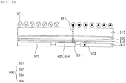
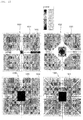
- FIGS. 5 to 6B are diagrams for explanation of a wireless charging pad according to an embodiment of the present invention.
- FIG. 5 is an exemplary exploded perspective view of a wireless charging pad.
- FIG. 6A is an exemplary top view of a wireless charging pad, which primarily shows a coil 520, a ferrite plate 510, and a resonance tank 530.
- FIG. 6B shows a side view of a wireless charging pad, which primarily shows the coil 520, the ferrite plate 510, and the resonance tank 530.
- a wireless charging pad 500 may include: a top case 610, a coil guide 620, at least one coil 520, at least one ferrite plate 510, an aluminum plate 630, an insulation sheet 640, a resonance tank 530, and a bottom case 650.
- a top case 610 may form the external appearance of the wireless charging pad 500 together with the bottom case 650.
- the top case 610 may be coupled to the bottom case 650 to form a space therebetween.
- the coil guide 620, the at least one coil 520, the at least one ferrite plate 510, the aluminum plate 630, the insulation sheet 640, and the resonance tank 530 may be accommodated in the space formed by the top case 610 and the bottom case 650.
- the coil guide 620 may be disposed on the at least one coil 520.
- the coil guide 620 may restrict the at least one coil 520 so that the at least one coil 1520 is fixed and not allowed to move.
- the at least one coil 520 may be formed in spiral, and have a shape that is a circular, elliptical, or polygonal.
- the coil guide 620 may have a shape capable of accommodating a circular, elliptical, or a polygonal shape.
- the coil guide 620 may be integrally formed with the top case 610.
- the coil guide 620 may be omitted.
- the at least one coil 520 may be a coil for power transmission.
- the at least one coil 520 may be disposed on the at least one ferrite plate 510.
- the at least one coil 520 may be described as the transmitting coil 15.
- the at least one coil 520 may be described as the receiving coil 25.
- the at least one coil 520 may be formed in spiral.
- the at least one coil 520 may be wound to thereby have an external appearance that is circular, elliptical, or polygonal.
- the at least one coil 520 may include a first end 521 and a second end 529.
- the first end 521 may function as an input end or an output end of the wireless charging pad 500.
- the second end 529 may be connected with at least one flat type capacitor 600 of the resonance tank 530 by a first wire 611.
- the at least one coil 520 may be positioned between the coil guide 620 and the at least one ferrite plate 510.
- the at least one ferrite plate 510 may have a shape of a circular, elliptical, or polygonal plate.
- the at least one ferrite plate 510 may be formed in plural.
- the at least one ferrite plate 510 may include a hole 511 that penetrates a top surface and a bottom surface of the at least one ferrite plate 510.
- the top surface of the at least one ferrite plate 510 may be defined as a surface that faces at least one of the top case 610, the coil guide 620 or the at least one coil 520.
- the bottom surface of the at least one ferrite plate 510 may be defined as a surface that faces at least one of the aluminum plate 630, the insulation sheet 640, the resonance tank 530, or the bottom case 650.
- the at least one ferrite plate 510 may include a groove 512 formed in the bottom surface thereof.
- the at least one ferrite plate 510 may be positioned between the at least one coil 520 and the resonance tank 530.
- the aluminum plate 630 and the insulation sheet 640 may be positioned between the at least one ferrite plate 510 and the resonance tank 530.
- the aluminum plate 630 may shield a magnetic field.
- the aluminum plate 630 may shield may shield a magnetic field generated in the course of power transmission and/or power reception, so that leakage of the magnetic field is prevented.
- the aluminum plate 630 may perform a heat dissipating function.
- the aluminum plate 630 may induce, to the outside of the wireless charging pad 500, heat that is generated in the at least one coil 520 and/or the at least one ferrite plate 510 in the course of power transmission and/or power reception.
- the aluminum plate 630 may be positioned between the at least one ferrite plate 510 and the bottom case 650.
- the aluminum plate 630 may be disposed under the at least one ferrite plate 510.
- the aluminum plate 630 may have a hole formed therein to insert the first wire 611.
- the insulation sheet 640 may shield an undesired current.
- the insulation sheet 640 may shield a surface current flowing on the at least one ferrite plate 510.
- the insulation sheet 640 may shield a current, so that a capacitor of the resonance tank 530 is electrically isolated from other elements of the wireless charging pad 500.
- the insulation sheet 640 may be positioned between the at least one ferrite plate 510 and the bottom case 650.
- the insulation sheet 640 may be positioned between the aluminum plate 630 and the at least one flat type capacitor 600.
- the insulation sheet 640 may have a hole formed therein to insert the first wire 611.
- the resonance tank 530 may be called a tank circuit, a resonance circuit, a resonance tank, a resonance tank circuit, or the like.
- the resonance tank 530 may be provided to compensate for an impedance of the at least one coil 520.
- the resonance tank 530 may include the at least one flat type capacitor 600.
- a resonance tank 530 according to a conventional technology is included in a circuit, separately from a transmitting pad 14 or a receiving pad 21.
- the resonance tank 530 when the resonance tank 530 according to the conventional technology is coupled to a product made by a different company, it is inevitable to modify a case and a heat dissipating structure in order to modify a parameter for a resonance part included in the circuit.
- the wireless charging pad 500 since the wireless charging pad 500 according to the present invention includes the resonance tank 530, the wireless charging pad 500 may be coupled to a product by a different company if a flat type capacitor is changed. That is, the wireless charging pad 500 has an advantage in that it is easy to modify a parameter for the resonance part. In addition, the parameter for the resonance part may be modified even without changing a cooling structure or an external appearance by changing molding of the wireless charging pad 500.
- the external appearance of the wireless charging pad 500 may be formed flat. Due to the flat external appearance, it is easy (for a transmitting pad) to be installed at the ground or (for a receiving pad) to be installed in a vehicle.
- the at least one flat type capacitor 600 may be disposed under the at least one ferrite plate 510.
- the at least one flat type capacitor 600 may be electrically connected with the at least one coil 520 by the first wire 611 inserted through the hole 511.
- the at least one flat type capacitor 600 may be electrically connected with an external device by a second wire 612 disposed in the groove 512.
- the external device may refer to a device external to the wireless charging pad 500.
- the external device when the wireless charging pad 500 is used as the transmitting pad 14, the external device may be a circuit.
- the circuit may be a concept including at least one of the DC/AC inverter 12, the AC/DC converter 11, or the grid 1.
- the external device may be a circuit.
- the circuit may be a concept including the rectifier 23 or the battery 30.
- the at least one flat type capacitor 600 may be configured in plural.
- the at least one flat type capacitor 600 may include a first capacitor 601 and a second capacitor 602.
- the first capacitor 601 may be connected in series with the at least one coil 520 by the first wire 611.
- the second capacitor 02 may be connected in series with the first capacitor 601.
- the second capacitor 602 may be connected in parallel with the first capacitor 601.
- the second capacitor 602 may be connected with an external device by the second wire 612.
- At least one capacitor 603 or 604 may be connected in series between the first capacitor 601 and the second capacitor 602.
- Capacitance may be adjusted according to the number of plural capacitors connected in series between the first capacitor 601 and the second capacitor 602.
- Capacitance may be adjusted according to in-series or in-parallel connection of plural capacitors including the first capacitor 601 and the second capacitor 602.
- the second wire 612 may include a first end 621 and a second 629.
- the first end 621 may be connected with the at least one flat type capacitor 600.
- the second end 629 may be connected with an external device.
- the second end 629 may function as an input end or an output end of the wireless charging pad 500.
- the second end 629 of the second wire 612 may function as an output end of the wireless charging pad 500.
- the second end 629 of the second wire 612 may function as an input end of the wireless charging pad 500.
- the resonance tank 530 may be positioned between the at least one ferrite plate 510 and the bottom case 650.
- the aluminum plate 630, the insulation sheet 640, and the resonance tank 530 may be arranged in different order from FIG. 5 between the bottom case 650 and the at least one ferrite plate 510.
- the insulation sheet 640, the aluminum plate 630, and the resonance tank 530 may be arranged in order.
- the resonance tank 530, the insulation sheet 640, and the aluminum plate 630 may be arranged in order.
- the resonance tank 530, the aluminum plate 630, and the insulation sheet 640 may be arranged in order.
- the bottom case 650 may form an external appearance of the wireless charging pad 500 together with the top case 610.
- the bottom case 650 may be coupled to the top case 610 to form a space therebetween.
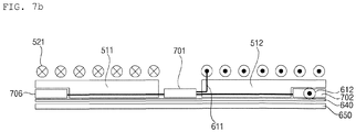
- FIGS. 7A and 7B are diagrams for explanation of a wireless charging pad according to an embodiment of the present invention.
- FIGS. 6A and 6B may apply to a wireless charging pad in FIGS. 7A and 7B .
- the at least one ferrite plate 510 may include a plurality of ferrites 511, 512, 513, 514, 515, and 516.
- the at least one ferrite plate 510 may include first to sixth ferrites 511, 512, 513, 514, 515, and 516.
- Each of the plurality of ferrites 511, 512, 513, 514, 515, and 516 may have a shape defined by two straight lines, a first arc connected to the two straight lines, and a second arc having a radius greater than a radius of the first arc.
- Each of the plurality of ferrites 511, 512, 513, 514, 515, and 516 may be described as a fan shape that is hollow.
- the structure of the ferrites allows the at least one coil 520 to be wound in a circular type, thereby increasing efficiency in wireless power transmission.
- a plurality of flat type capacitor 600 may be interposed between any two of the plurality of ferrites 511, 512, 513, 514, 515, and 516.
- the at least one flat type capacitor 600 may include a plurality of capacitors 701, 702, 703, 704, 705, and 706.
- the at least one flat type capacitor 600 may include first to sixth capacitors 701, 702, 703, 704, 705, and 706.
- the first capacitor 701 may be positioned between the first plate 511 and the second plate 512.
- the first capacitor 701 may be connected in series with the at least one coil 520 by the first wire 611.
- the second capacitor 702 may be positioned between the second plate 512 and the third plate 513.
- the second capacitor 702 may be connected in series with the first capacitor 701.
- the second capacitor 702 may be connected in parallel with the first capacitor 701.
- the second capacitor 702 may be connected with an external device by the second wire 612.
- At least one capacitor 703, 704, 705, or 706 may be connected in series between the first capacitor 701 and the second capacitor 702.
- Capacitance may be adjusted according to the number of plural capacitors connected in series between the first capacitor 701 and the second capacitor 702.
- Capacitance may be adjusted according to in-series or in-parallel connection of plural capacitors including the first capacitor 701 and the second capacitor 702.
- FIGS. 8A to 8C are diagrams for explanation of a wireless charging pad according to an embodiment of the present invention.
- the description about the wireless charging pad in FIGS. 6A and 6B , and the description about the wireless charging pad in FIGS. 7A to 7C may apply to a wireless charging pad in FIGS. 8A to 8C .
- the at least one coil 520 may include a plurality of sub-coils 520a, 520b, 520c, 520d, 520e, and 520f.
- the at least one coil 520 may include first to sixth sub-coils 520a, 520b, 520c, 520d, 520e, and 520f.
- the at least one coil 520 may include sub-coils 520a, 520b, 520c, 520d, 520e, and 520f in the same number of the plural capacitors 701, 702, 703, 704, 705, and 706.
- the at least one flat type capacitor 600 may include the plurality of capacitors 701, 702, 703, 704, 705, and 706.
- the at least one flat type capacitor 600 may include first to sixth capacitors 701, 702, 703, 704, 705, and 706.
- the plurality of sub-coils 520a, 520b, 520c, 520d, 520e, and 520f may be alternately connected in series with the plurality of capacitors , 702, 703, 704, 705, and 706.
- the insulation sheet 640 may be disposed under the at least one ferrite plate 510 and the at least one flat type capacitor 600.
- the aluminum plate 630 may be disposed under the insulation sheet 640.
- FIG. 8C shows an exemplary equivalent circuit for connection between a plurality of sub-coils and a plurality of capacitors.
- the plurality of sub-coils 520a, 520b, 520c, 520d, 520e, and 520f and the plurality of capacitors , 702, 703, 704, 705, and 706 may be alternately connected in series.
- the first sub-coil 520a may be connected with the second capacitor 702.
- the second sub-coil 520b may be connected with the second capacitor 702 and the fifth capacitor 705.
- the third sub-coil 520c may be connected with the fifth capacitor 705 and the first capacitor 701.
- the fourth sub-coil 520d may be connected with the first capacitor 701 and the fourth capacitor 704.
- the fifth sub-coil 520e may be connected with third capacitor 703 and the sixth capacitor 706.
- the sixth sub-coil 520f may be connected with the sixth capacitor 706.
- FIGS. 6A to 8B show examples of the wireless charging pad 500 and the scope of the present invention is not limited by the number of ferrites and the number of capacitors.
- FIGS. 9 and 10 are diagrams for explanation of a flat type capacitor according to an embodiment of the present invention.
- FIG. 9 shows an example of a flat type capacitor 600 that uses a ceramic material.
- Reference numeral 910 refers to a ceramic capacitor 600.
- a flat type ceramic capacitor bank with an optimum size may be configured.
- FIG. 10 shows an example of a flat type capacitor 600 that uses a film.
- electrode plates 1020 are attached to both surfaces of the film dielectric 1010 and deposited, and then, if the both surfaces are connected (x), a film type capacitor 600 having a parallel structure may be achieved.
- the flat type capacitor 600 may be defined as a structure included in the wireless charging pad 500 using a large and thin capacitor, which is not the same as shown in FIGS. 9 and 10 , though.
- the wireless charging pad 500 has a structure of large plates, if the flat type capacitor 600 is disposed under the at least one ferrite plate 510 or interposed between a plurality of plates 511, 512, 513, 514, 515, and 516, it is possible to remove a resonance part from a circuit and minimize increase in volume of the wireless charging pad 500.
- an induced voltage be3tween an input end and an output end of the wireless charging pad is significantly reduced, thereby decreasing the need for an insulation distance.
- FIG. 11 is a diagram for explanation of configuration of a wireless charging pad according to an embodiment of the present invention.
- FIG. 11 shows an exploded perspective view of a wireless charging pad.
- FIG. 11 is described by exemplifying a receiving pad 21.
- Elements of a transmitting pad 14 are deposited on the basis of the ground in order reverse to the order in which elements of the receiving pad 21 are deposited, but the description about FIG. 11 may apply to the transmitting pad 14.
- a wireless charging pad 500 may include a first case 1610, a coil guide 1620, at least one coil 1520, a first magnetic body 1511, a second magnetic body 1512, an aluminum plate 1630, an insulation sheet 1640, and a second case 1650.
- the first case 1610 may form an external appearance of the wireless charging pad 500 together with the second case 1650.
- the first case 1610 may be coupled to the second case 1650 to form a space therebetween.
- the coil guide 1620, the at least one coil 1520, the first magnetic body (or ferrite plate) 1511, the second magnetic body 1512, the aluminum plate 1630, and the insulation sheet 1640 may be accommodated in the space formed by the first case 1610 and the second case 1620.
- the coil guide 1620 may be disposed over or under the at least one coil 1520. When coupled to the at least one coil 1520, the coil guide 1620 may restrict the at least one coil 1520 so that the at least one coil 1520 is fixed and not allowed to move. In some embodiments, the coil guide 1620 may be integrally formed with the first case 1610. In some embodiments, the coil guide 1620 may be omitted.
- the at least one coil 1520 may be formed in spiral and have a shape that is circular, elliptical, or polygona.
- the coil guide 1620 may have a shape capable of accommodating a circular, elliptical, or polygonal shape.
- the at least one coil 1520 may be a coil for power transmission.
- the at least one coil 1520 may transmit or receive power wirelessly.
- the wireless charging pad 500 functions as the transmitting pad 14
- the at least one coil 1520 may be described as the transmitting coil 15.
- the wireless charging pad 500 functions as the receiving pad 15, the at least one coil 1520 may be described as the receiving coil 15.
- the at least one coil 1520 may be formed in spiral.
- the at least one coil 1520 may be wound to thereby have an external appearance that is circular, elliptical, or polygonal.
- the at least one coil 1520 may include a lead-in wire and a lead-out wire.
- the first magnetic body 1511 may have a circular, elliptical, or polygonal shape.
- a magnetic body 510 may be configured as at least one plate. It is preferable that the first magnetic body 1511 uses a ferrite.
- the first magnetic body 1511 may be referred to as a first ferrite plate.
- the first magnetic body 1511 may be disposed to form layers with the second magnetic body 1512.
- the first magnetic body 1511 may be disposed over or under the second magnetic body 1512.
- the first magnetic body 1511 may be disposed on the same layer of the at least one coil 1520.
- the second magnetic body 1512 may have a circular, elliptical, or polygonal shape.
- the magnetic body 510 may be configured as at least one plate.
- the magnetic body 510 may include a plurality of plates arranged side by side. It is preferable that the second magnetic body 1512 uses ferrite.
- the second magnetic body 1512 may be referred to as a second ferrite plate.
- the second magnetic body 1512 may be disposed to form layers with the first magnetic body 1511.
- the second magnetic body 1512 may be disposed over or under the first magnetic body 1511.
- the second magnetic body 1512 may be disposed to form layers with the at least one coil 1520.
- the second magnetic body 1512 may be disposed over or under the at least one coil 1520.
- the insulation sheet 1640 may shield an undesired current.
- the insulation sheet 1640 may shield a surface current flowing in the magnetic body 510.
- the insulation sheet 1640 may shield a current so that a capacitor of a resonance tank is electrically isolated from other elements of the wireless charging pad 500.
- the insulation sheet 1640 may be interposed between the aluminum plate 1630 and the magnetic body 510.
- the insulation sheet 1640 may be formed of any of various insulating materials, but it is preferably that the insulation sheet 1640 is formed of a polycarbonate (PC) material.
- PC polycarbonate
- the aluminum plate 1630 may shield a magnetic field.
- the aluminum plate 1630 may shield a magnetic field generated in the course of power transmission and/or power reception, so that leakage of the magnetic field is prevented.
- the aluminum plate 1630 may perform a heat dissipating function.
- the aluminum plate 1630 may induce, to the outside of the wireless charging pad 500, heat that is generated in the at least one coil 1520 and/or the magnetic bodies 1511 and 1512 in the course of power transmission and/or power reception.
- the aluminum plates 1630 may be interposed between the first and second magnetic bodies 1511 and 1512 and the second case 1650.
- the aluminum plate 1630 may be disposed under the first and second magnetic bodies 1511 and 1512.
- the second case 1650 may form an external appearance of the wireless charging pad 500 together with the first case 1610.
- the second case 1650 may be coupled to the first case 1610 to form a space therebetween.
- FIGS. 12 to 14 are diagrams for explanation of a wireless charging pad according to an embodiment of the present invention.
- FIGS. 12 to 14 are described by exemplifying a receiving pad 21. Elements of a transmitting pad 14 are deposited on the basis of the ground in order reverse to the order in which elements of the receiving pad 21 are deposited, and the description about FIG. 12 to 14 may apply to the transmitting pad 14.
- FIG. 12 is a bottom view of a wireless charging pad according to an embodiment of the present invention
- FIG. 13 is a side view of a wireless charging pad according to an embodiment of the present invention from a direction indicated by an arrow in FIG. 12 .
- a first magnetic body 1511 may be disposed to form layers with a second magnetic body 1512.
- the first magnetic body 1511 may be deposited on the second magnetic body 1512 or the second magnetic body 1512 may be deposited on the first magnetic body 1511. At least part of the first magnetic body 1511 may be in contact with at least part of the second magnetic body 1512.
- the first magnetic body 1511 may be disposed on the same layer of a coil 1520. At least part of the first magnetic body 1511 may be vertically overlaid with a space 1513 of the second magnetic body 1512.
- the second magnetic body 1512 may be disposed to form layers with the first magnetic body 1511. At least part of the second magnetic body 1512 may be in contact with at least part of the first magnetic body 1511. Since the second magnetic boy 1512 and the first magnetic body 1511 are in contact with each other, a continuous magnetic path may be formed in the first magnetic body 1511 and the second magnetic body 1512.
- the second magnetic body 1512 may provide a space 1513 where at least one electronic component is accommodated. Due to the continuous magnetic path in the first magnetic body 1511 and the second magnetic body 1512, an eddy current is prevented from affecting the electronic component accommodated within the second magnetic body 1512, and therefore, influence from EMC is minimized and heat by a magnetic field is not generated in the electronic component. At least part of the space 1513 of the second magnetic body 1512 may be vertically overlaid with the first magnetic body 1511.
- the electronic component may include at least one of a converter, an inverter, a rectifier, or a resonance tank.
- the electronic component may include at least one of the resonance tank 22 or the rectifier 23.
- the wireless charging pad 500 functions as a transmitting pad 14, the electronic component may include at least one of an AC/DC converter, a DC/AC inverter 12, or a resonance tank 13.
- a positional relationship of a first magnetic body 1511, a second magnetic body 1512, and a coil 1520 may be described with reference to layers.
- the first layer 1531 may be described as a layer different from a second layer 1532. As shown in FIG. 13 , the second layer 1532 may be disposed over the first layer 1531 in a direction upward from the ground. In some embodiments, the first layer 1531 may be disposed over the second layer 1532 in the direction upward from the ground.
- the first magnetic body 1511 and the coil 1520 may be disposed on the first layer 1531.
- the second magnetic body 1512 may be disposed on the second layer 1532. Since the first magnetic body 1511, the coil 1520, and the second magnetic body 1512 are disposed as described above, the second magnetic body 1512 may be disposed to form layers with the first magnetic body 1511 and the coil 1520.
- the space 1513 of the second magnetic body 1512 may be positioned on the second layer 1532. Accordingly, an electronic component in the space 1513 may be disposed on the second layer 1532.
- the coil 1520 may be wound around surroundings of the first magnetic body 1511.
- the wireless charging pad 500 may further include an insulator.
- the insulator may be disposed between the fist magnetic body 1511 and the coil 1520.
- the insulator may be formed to surround the first magnetic body 1511, and the coil 1520 may be wound to embrace the insulator. It is preferable that the insulator is formed of a polycarbonate (PC) material.
- the coil 1520 may be disposed over or under the second magnetic body 1512.
- the second magnetic body 1512 may include a plurality of sub-magnetic bodies 1512a, 1512b, 1512c, and 1512d.
- the plurality of sub-magnetic bodies 1512a, 1512b, 1512c, and 1512d may be spaced apart from each other at a predetermined interval. At least part of each of the plurality of sub-magnetic bodies 1512a, 1512b, 1512c, and 1512d may be in contact with at least part of the first magnetic body 1511. At least part of the first magnetic body 1511 may be in contact with at least part of each of the plurality of sub-magnetic bodies 1512a, 1512b, 1512c, and 1512d.
- a magnetic flux entering into the plurality of sub-magnetic bodies 1512a, 1512b, 1512c, and 1512d from a peripheral area does not flow in gaps between the plurality of sub-magnetic bodies 1512a, 1512b, 1512c, and 1512d, where reluctance is unlimited, but flows in the first magnetic boy 1511. Accordingly, a magnetic flux leakage may be reduced significantly.
- first magnetic body 1511 and the second magnetic body 1512 are disposed to be layered and at least part of the second magnetic body 1512 is in contact with at least part of the first magnetic body, a magnetic flux flowing into the internal space 1513 of the second magnetic body 1512 may be reduced significantly.
- the coil 1520 may include a lead-in wire 1521 and a lead-out wire 1522.
- the lead-in wire 1521 and the lead-out wire 1522 of the coil 1520 may be disposed in a gap formed between the plurality of sub-magnetic bodies.
- a first internal impedance value seen in an arrow direction by the lead-in wire 1521 and the lead-out wire 1522 with an electronic component being disposed in the space 1513 is smaller than a second internal impedance value seen by the lead-in wire 1521 and the lead-out wire 1522 with any electronic component being not disposed in the space 1513. While an electronic component is disposed in the space 1513, inductance of the coil 1520 is offset by capacitance of the resonance tank 13 or 22, and thus, an internal impedance value is reduced.
- the second magnetic body 1512 may include a plurality of sub-magnetic bodies 1512e, 1512f, 1512g, 1512h, 1512i, 1512j, 1512k, and 15121.
- the plurality of sub-magnetic bodies 1512e, 1512f, 1512g, 1512h, 1512i, 1512j, 1512k, and 15121 may have different shapes.
- the plurality of sub-magnetic bodies may include a first sub-magnetic body 1512e, a second sub-magnetic body 1512f, and a third sub-magnetic body 1512g.
- the second sub-magnetic body 1512f may be disposed in parallel with the first sub-magnetic body 1512e in a first direction.
- the second sub-magnetic body 1512f may be disposed in parallel with the third sub-magnetic body 1512g in a second direction different from the first direction.
- a first gap 1512m between the first sub-magnetic body 1512e and the second sub-magnetic body 1512f may be different from a second gap 1512n between the second sub-magnetic body 1512f and the third sub-magnetic body 1512g.
- FIG. 15 is a diagram for explanation experimental data for a wireless charging pad according to an embodiment of the present invention.
- reference numeral 1010 indicates a magnetic flux of when there is included only a second magnetic body 1512 comprised of a plurality of sub-magnetic bodies spaced apart from each other at a predetermined interval.
- Reference numeral 1020 indicates a magnetic flux of when a space to accommodate an electronic component is secured in a predetermined area at the center of the wireless charging pad 500 by removing a magnetic body from the second magnetic body 1512 in 1010.
- Reference numeral 1030 indicates a magnetic flux of when the first magnetic body 1511 is disposed to form layers with and be in contact with the second magnetic body 1512 in 1020.
- Reference numeral 1040 indicates a magnetic flux of when there are included sub-magnetic bodies more than in 1030.
- the greatest magnetic flux is found.
- a magnetic path connected between a plurality of sub-magnetic bodies is not secured, and thus, it is found that a magnetic flux linkage of a central area 1011 in 1010 is about 44,000 times greater than a magnetic flux linkage of a central area 1031 in 1030.
- a magnetic flux linkage of an area 1012 between sub-magnetic bodies in 1010 is about 250,000 times greater than a magnetic flux linkage of an area 1032 between sub-magnetic bodies in 1030.
- a Cu bus bar is positioned in the area 1012 between sub-magnetic bodies in 1010, it is found that the bus bar increases in temperature by about 40 degrees or more. Yet, in the case where the Cu bus bar is positioned in the area 1032 between sub-magnetic bodies in 1030, it is found that the bus bar increases in temperature by about 10 degrees or less.
- a magnetic flux linkage of the central area 1021 in 1020 is about 20,000 times greater than a magnetic flux linkage of the central area 1031 in 1030.
- the wireless charging pad 500 is less affected by magnetic flux linkage, and therefore, the wireless charging pad integrated with the electronic component may be provided.
Landscapes
- Engineering & Computer Science (AREA)
- Power Engineering (AREA)
- Computer Networks & Wireless Communication (AREA)
- Transportation (AREA)
- Mechanical Engineering (AREA)
- Charge And Discharge Circuits For Batteries Or The Like (AREA)
Abstract
Description
- The present invention relates to a wireless charging pad and a wireless charging apparatus.
- With relentless effort to study and develop various electronic devices, a wireless charging system for supplying electrical energy to an electronic device is also being studied.
- Many corporation and institutions have been making efforts to develop a wireless charging system of a mobile terminal and a wireless charging system for an electric vehicle. Such a wireless charging system requires various electronic components such as a wireless charging pad and a resonance tank for compensating for an impedance.
- International Patent Application Publication No.
WO 2014/179320 (hereinafter, referred to as Related Art 1) discloses a DDQ coil pad structure. A pad ofRelated Art 1 does not include a resonance part. A resonance tank in a wireless charging system according toRelated Art 1 is manufactured separately from a wireless charging pad, and, if a power transmitting apparatus is made by a manufacturer different from a manufacturer of a power receiving apparatus, a housing and a heat-dissipating structure should be changed in order to modify a parameter for the resonance part. Meanwhile, a high induced voltage occurs at both ends of a coil. The wireless charging pad according toRelated Art 1 has a structure in which one end of an wound coil comes out of the pad in order to secure an insulation distance. This structure causes a problem that the wireless charging pad has an increased volume and does not have a flat shape (hereinafter, referred to as the first problem). - Korean Patent Application Publication No.
10-2016-0008213 - In order to solve the first problem, the present invention provides a wireless charging pad having a resonance part of which a parameter is capable of being easily modified.
- In addition, the present invention provides a wireless charging pad which has a resonance having a parameter capable of being easily modified so that the wireless charging pad is able to be generalized, and which is capable of being manufactured in a slim shape using a flat type capacitor.
- In addition, the present invention provides a wireless charging pad capable of being made flat as there are provided a hole for inserting a wire into a plate and a groove for aligning the wire.
- In order to solve the second problem, the present invention provides a wireless charging pad capable of addressing heat emission and electric-Magnetic Compatibility (EMC) while accommodating an electronic component within a wireless charging pad.
- In addition, the present invention provides a wireless charging pad manufactured in a flat shape and thus having a minimum volume without an additional space for an electronic component.
- In addition, the present invention provides a wireless charging pad in which magnetic bodies are provided in two layers to position an electronic component in an empty space.
- Objects of the present invention should not be limited to the aforementioned objects and other unmentioned objects will be clearly understood by those skilled in the art from the following description.
- A wireless charging pad according to an embodiment of the present invention comprises a resonance tank configured to compensate for impedance. In addition, the resonance tank comprises a flat type capacitor.
- A wireless charging pad according to an embodiment of the present invention includes: at least one ferrite plate; a coil disposed on the at least one ferrite plate; and a resonance tank having at least one flat type capacitor to compensate for an impedance of the coil.
- The at least one flat type capacitor may be disposed under the ferrite plate.
- The at least one ferrite plate may include a hole penetrating a top surface and a bottom surface of the at least one ferrite plate, and the at least one flat type capacitor may be electrically connected with the coil by a first wire inserted through the hole.
- The at least one ferrite plate may include a groove formed in the bottom surface, and the at least one flat type capacitor may be electrically connected with an external device by a second wire disposed in the groove.
- The at least one flat type capacitor may include: a first capacitor connected in series with the coil by the first wire; and a second capacitor connected in series with the first capacitor and connected with the external device by the second wire.
- The wireless charging pad may further include: an aluminum plate disposed under the ferrite plate; and an insulation sheet interposed between the aluminum plate and the at least one flat type capacitor.
- The at least one ferrite plate may include a plurality of ferrites, and wherein the at least one flat type capacitor may be interposed between any two of the plurality of ferrites.
- The at least one flat type capacitor may include: a first capacitor connected in series with the coil; and a second capacitor connected in series with the first capacitor.
- The coil may include a plurality of sub-coils, the at least one flat type capacitor may include a plurality of capacitors, and the plurality of sub-coils and the plurality of capacitors may be alternately connected in series.
- Each of the plurality of ferrites may have a shape defined by two straight lines, a first arc connected to the two straight lines, and a second arc having a radius greater than a radius of the first arc.
- The wireless charging pad may include magnetic bodies to be layered.
- A wireless charging pad according to an embodiment of the present invention includes: a first ferrite plate; a second ferrite plate disposed to form layers with the first ferrite plate; and a coil wound around surroundings of the first ferrite plate, and disposed over or under the second ferrite plate.
- At least part of the second ferrite plate may be in contact with at least part of the first ferrite plate.
- A continuous magnetic path may be formed in the first ferrite plate and the second ferrite plate.
- The second ferrite plate may provide a space to accommodate at least one electronic component.
- At least part of the first ferrite part may be vertically overlaid with the space.
- The first ferrite plate and the coil may be disposed on a first layer, and the second ferrite plate may be disposed on the second layer.
- The at least one electronic component may be disposed on the second layer, and the at least one electronic component may include at least one of a converter, an inverter, a rectifier, or a resonance tank.
- The second ferrite plate may include a plurality of sub-magnetic bodies, and the coil may include a lead-in wire and a lead-out wire disposed in a gap formed between the plurality of sub-magnetic bodies.
- A first internal impedance value seen from the lead-in wire and the lead-out wire with the at least one electronic component being disposed in the space may be smaller than a second internal impedance value seen from the lead-in wire and the lead-out wire with the at least one electronic component being not disposed in the space.
- The wireless charging pad may further include an insulator disposed between the first ferrite plate and the coil.
- The details of other embodiments are included in the following description and the accompanying drawings.
- According to the present invention, there are one or more effects as below.
- First, as a resonance tank is included, it is possible to generalize a wireless charging pad.
- Second, as a flat type capacitor is included in a resonance tank, it is possible to manufacture a wireless charging pad in a slim shape.
- Third, as a hole and a groove are provided in a ferrite plate, it is possible to manufacture a wireless charging pad in a flat shape.
- Fourth, as electronic components such as a resonance tank is included in a wireless charging pad, it is possible to easily modify a parameter for a resonance part and easily generalize a wireless charging pad.
- Fifth, it is possible to minimize a volume of a wireless charging pad even without an additional space for an electronic component such as a resonance tank.
- Sixth, it is possible to manufacture a wireless charging pad in a flat shape.
- Effects of the present invention should not be limited to the aforementioned effects, and effects that have not been mentioned above or additional effects of the present application may become apparent to those having ordinary skill in the art from the description presented below.
-
-
FIG. 1 is a diagram showing an external appearance of a wireless charging system according to an embodiment of the present invention. -
FIG. 2 is a block diagram of a wireless charging system according to an embodiment of the present invention. -
FIG. 3 is a diagram for explanation of a wireless charging method according to an embodiment of the present invention. -
FIG. 4 shows an example of an equivalent circuit of a wireless charging pad according to an embodiment of the present invention. -
FIGS. 5 to 6B are diagrams for explanation of a wireless charging pad according to an embodiment of the present invention. -
FIGS. 7A and7B are diagrams for explanation of a wireless charging pad according to an embodiment of the present invention. -
FIGS. 8A to 8C are diagrams for explanation of a wireless charging pad according to an embodiment of the present invention. -
FIGS. 9 and10 are diagrams for explanation of a flat type capacitor according to an embodiment of the present invention. -
FIG. 11 is a diagram for explanation of configuration of a wireless charging pad according to an embodiment of the present invention. -
FIGS. 12 to 14 are diagrams for explanation of a wireless charging pad according to an embodiment of the present invention. -
FIG. 15 is a diagram for explanation experimental data for a wireless charging pad according to an embodiment of the present invention. - Hereinafter, the embodiments disclosed in the present specification will be described in detail with reference to the accompanying drawings, and the same or similar elements are denoted by the same reference numerals even though they are depicted in different drawings and redundant descriptions thereof will be omitted. In the following description, with respect to constituent elements used in the following description, the suffixes "module" and "unit" are used or combined with each other only in consideration of ease in the preparation of the specification, and do not have or serve as different meanings. Accordingly, the suffixes "module" and "unit" may be interchanged with each other. In addition, in the following description of the embodiments disclosed in the present specification, a detailed description of known functions and configurations incorporated herein will be omitted when it may make the subject matter of the embodiments disclosed in the present specification rather unclear. In addition, the accompanying drawings are provided only for a better understanding of the embodiments disclosed in the present specification and are not intended to limit the technical ideas disclosed in the present specification. Therefore, it should be understood that the accompanying drawings include all modifications, equivalents and substitutions included in the scope and sprit of the present invention.
- It will be understood that although the terms "first," "second," etc., may be used herein to describe various components, these components should not be limited by these terms. These terms are only used to distinguish one component from another component.
- It will be understood that when a component is referred to as being "connected to" or "coupled to" another component, it may be directly connected to or coupled to another component or intervening components may be present. In contrast, when a component is referred to as being "directly connected to" or "directly coupled to" another component, there are no intervening components present.
- As used herein, the singular form is intended to include the plural forms as well, unless the context clearly indicates otherwise.
- In the present application, it will be further understood that the terms "comprises", "includes," etc. specify the presence of stated features, integers, steps, operations, elements, components, or combinations thereof, but do not preclude the presence or addition of one or more other features, integers, steps, operations, elements, components, or combinations thereof.
-
FIG. 1 is a diagram showing an external appearance of a wireless charging system according to an embodiment of the present invention. -
FIG. 2 is a block diagram of a wireless charging system according to an embodiment of the present invention. - Referring to the drawings, a
wireless charging system 100 may include apower transmitting apparatus 10 and apower receiving apparatus 20. Thewireless charging system 100 may be used for wireless charging of an electric vehicle battery, wireless charging of a robot cleaner, wireless charging of a mobile terminal battery, etc. - In the case where the
wireless charging system 100 is used for wireless charging of an electric vehicle battery, thepower transmitting apparatus 10 may be installed at a charging station or the like, and thepower receiving apparatus 20 may be provided in a vehicle. In the case where thewireless charging system 100 is used for wireless charging of a robot cleaner, thepower transmitting apparatus 10 may be configured as a portable type, and thepower receiving apparatus 20 may be provided in the robot cleaner. In the case where thewireless charging system 100 is used for wireless charging of a mobile terminal battery, thepower transmitting apparatus 10 may be configured as a portable type, and thepower receiving apparatus 20 may be provided in a mobile terminal. - The
power transmitting apparatus 10 may include an AC/DC converter 11, a DC/AC inverter 12, aresonance tank 13, and atransmitting pad 14. The AC/DC converter 11 may convert AC electrical energy provided from agrid 1 into DC electrical energy. The DC/AC inverter 12 converts the DC electric energy into AC electric energy. In this case, the DC/AC inverter 12 may generate a high-frequency signal of few dozens or hundreds of kHz. Theresonance tank 13 compensate for impedance appropriately for wireless charging. The transmittingpad 14 transmits electrical energy wirelessly. The transmittingpad 14 includes a transmittingcoil 15. - The
power receiving apparatus 20 may include areceiving pad 21, aresonance tank 22, and arectifier 23. The receivingpad 21 receives electric energy wirelessly. The receivingpad 21 includes a receivingcoil 25. The transmittingpad 14 and the receivingpad 21 include a coil set (the transmittingcoil 15 and the receiving coil 25) having magnetic coupling. The transmittingpad 14 and the receivingpad 21 delivers electric energy through a medium of a magnetic field without physical electrical contact between electrodes. Theresonance tank 22 compensates for impedance appropriately for wireless charging. Therectifier 21 converts AC electric energy into DC electric energy to supply the DC electric energy to thebattery 30. -
FIG. 3 is a diagram for explanation of a wireless charging method according to an embodiment of the present invention. - Referring to
FIG. 3 , the wireless charging system may employ inductive coupling or resonance coupling. - Inductive coupling works on the principle that, when intensity of a current flowing in a primary coil between two adjacent coils is changed, a magnetic field is changed by the current and in turn a magnetic flux passing through a secondary coil is changed to thereby generate an induced electromotive force on the side of the secondary coil. That is, if two coils are placed close to each other and only a current of the primary coil is changed, an induced electromotive force may be generated even though two wires are not moved spatially. In this case, frequency characteristics are not influenced greatly. However, power efficiency may be affected depending on alignment and distance between a transmitting apparatus (for example, a wireless charging apparatus) including the respective coils and a receiving apparatus (for example, a mobile terminal).
- Resonance coupling works on the principle that, when two coils are at a specific distance, a resonant frequency is applied to a primary coil between the two coils to thereby generate variation of a magnetic field and some of the variation is applied to a secondary coil having the same resonant frequency to thereby generate an induced electromotive force. According to this method, if a transmitter and a receiver resonate at the same frequency, a magnetic wave is transferred through a near magnetic field. Thus, if the transmitter and the receiver have different frequencies, energy is not transferred therebetween. In this case, selecting a frequency may be important. Energy is not transferred between resonant frequencies which are at a specific distance or more, and a device to be charged may be selected by selecting a resonant frequency. If a single device is allocated to each resonant frequency, selecting a resonant frequency may be equivalent to selecting a device to be charged.
- Resonance coupling has advantages over inductive coupling in that power efficiency is relatively less affected by alignment of a transmitter, including the respective coils, and a receiver and a distance between the transmitter and the receiver.
-
FIG. 4 shows an example of an equivalent circuit of a wireless charging pad according to an embodiment of the present invention. - A
wireless charging pad 500 according to an embodiment of the present invention may be used as atransmitting pad 14 of apower transmitting apparatus 10 or areceiving pad 21 of apower receiving apparatus 20. Thewireless charging pad 500 may be used for wireless charging of a small-sized device such as a mobile terminal, but it is preferable that thewireless charging pad 500 is used for wireless charging of a large-sized device such as an electric vehicle. - Referring to
FIG. 4 , thewireless charging pad 500 may be used as apower transmitting pad 500a or apower receiving pad 500b. Thepower transmitting pad 500a may include aresonance tank 13 and apower transmitting coil 520a. Thepower transmitting pad 500a may be electrically connected with apower converter power converter DC converter 11 and the DC/AC converter 12 described above with reference toFIG. 2 . Thepower receiving pad 500b may include aresonance tank 22 and apower receiving coil 520b. Thepower receiving pad 500b may be electrically connected with arectifier 23. -
FIGS. 5 to 6B are diagrams for explanation of a wireless charging pad according to an embodiment of the present invention. -
FIG. 5 is an exemplary exploded perspective view of a wireless charging pad. -
FIG. 6A is an exemplary top view of a wireless charging pad, which primarily shows acoil 520, aferrite plate 510, and aresonance tank 530. -
FIG. 6B shows a side view of a wireless charging pad, which primarily shows thecoil 520, theferrite plate 510, and theresonance tank 530. - Referring to
FIGS. 5 to 6B , awireless charging pad 500 may include: atop case 610, acoil guide 620, at least onecoil 520, at least oneferrite plate 510, analuminum plate 630, aninsulation sheet 640, aresonance tank 530, and abottom case 650. - A
top case 610 may form the external appearance of thewireless charging pad 500 together with thebottom case 650. - The
top case 610 may be coupled to thebottom case 650 to form a space therebetween. Thecoil guide 620, the at least onecoil 520, the at least oneferrite plate 510, thealuminum plate 630, theinsulation sheet 640, and theresonance tank 530 may be accommodated in the space formed by thetop case 610 and thebottom case 650. - The
coil guide 620 may be disposed on the at least onecoil 520. - When coupled to the at least one
coil 1520, thecoil guide 620 may restrict the at least onecoil 520 so that the at least onecoil 1520 is fixed and not allowed to move. - The at least one
coil 520 may be formed in spiral, and have a shape that is a circular, elliptical, or polygonal. Thecoil guide 620 may have a shape capable of accommodating a circular, elliptical, or a polygonal shape. - In some embodiments, the
coil guide 620 may be integrally formed with thetop case 610. - In some embodiments, the
coil guide 620 may be omitted. - The at least one
coil 520 may be a coil for power transmission. The at least onecoil 520 may be disposed on the at least oneferrite plate 510. - When the
wireless charging pad 500 functions as the transmittingpad 14, the at least onecoil 520 may be described as the transmittingcoil 15. - When the
wireless charging pad 500 functions as the receivingpad 15, the at least onecoil 520 may be described as the receivingcoil 25. - The at least one
coil 520 may be formed in spiral. - The at least one
coil 520 may be wound to thereby have an external appearance that is circular, elliptical, or polygonal. - The at least one
coil 520 may include afirst end 521 and asecond end 529. - The
first end 521 may function as an input end or an output end of thewireless charging pad 500. - The
second end 529 may be connected with at least oneflat type capacitor 600 of theresonance tank 530 by afirst wire 611. - The at least one
coil 520 may be positioned between thecoil guide 620 and the at least oneferrite plate 510. - The at least one
ferrite plate 510 may have a shape of a circular, elliptical, or polygonal plate. - In some embodiments, the at least one
ferrite plate 510 may be formed in plural. - The at least one
ferrite plate 510 may include ahole 511 that penetrates a top surface and a bottom surface of the at least oneferrite plate 510. - The top surface of the at least one
ferrite plate 510 may be defined as a surface that faces at least one of thetop case 610, thecoil guide 620 or the at least onecoil 520. - The bottom surface of the at least one
ferrite plate 510 may be defined as a surface that faces at least one of thealuminum plate 630, theinsulation sheet 640, theresonance tank 530, or thebottom case 650. - The at least one
ferrite plate 510 may include agroove 512 formed in the bottom surface thereof. - The at least one
ferrite plate 510 may be positioned between the at least onecoil 520 and theresonance tank 530. - In some embodiments, the
aluminum plate 630 and theinsulation sheet 640 may be positioned between the at least oneferrite plate 510 and theresonance tank 530. - The
aluminum plate 630 may shield a magnetic field. - The
aluminum plate 630 may shield may shield a magnetic field generated in the course of power transmission and/or power reception, so that leakage of the magnetic field is prevented. - The
aluminum plate 630 may perform a heat dissipating function. - The
aluminum plate 630 may induce, to the outside of thewireless charging pad 500, heat that is generated in the at least onecoil 520 and/or the at least oneferrite plate 510 in the course of power transmission and/or power reception. - The
aluminum plate 630 may be positioned between the at least oneferrite plate 510 and thebottom case 650. - For example, the
aluminum plate 630 may be disposed under the at least oneferrite plate 510. - Meanwhile, the
aluminum plate 630 may have a hole formed therein to insert thefirst wire 611. - The
insulation sheet 640 may shield an undesired current. - For example, the
insulation sheet 640 may shield a surface current flowing on the at least oneferrite plate 510. - For example, the
insulation sheet 640 may shield a current, so that a capacitor of theresonance tank 530 is electrically isolated from other elements of thewireless charging pad 500. - The
insulation sheet 640 may be positioned between the at least oneferrite plate 510 and thebottom case 650. - For example, the
insulation sheet 640 may be positioned between thealuminum plate 630 and the at least oneflat type capacitor 600. - Meanwhile, the
insulation sheet 640 may have a hole formed therein to insert thefirst wire 611. - The
resonance tank 530 may be called a tank circuit, a resonance circuit, a resonance tank, a resonance tank circuit, or the like. - The
resonance tank 530 may be provided to compensate for an impedance of the at least onecoil 520. - The
resonance tank 530 may include the at least oneflat type capacitor 600. - A
resonance tank 530 according to a conventional technology is included in a circuit, separately from a transmittingpad 14 or areceiving pad 21. - In this case, when the
resonance tank 530 according to the conventional technology is coupled to a product made by a different company, it is inevitable to modify a case and a heat dissipating structure in order to modify a parameter for a resonance part included in the circuit. - Since the
wireless charging pad 500 according to the present invention includes theresonance tank 530, thewireless charging pad 500 may be coupled to a product by a different company if a flat type capacitor is changed. That is, thewireless charging pad 500 has an advantage in that it is easy to modify a parameter for the resonance part. In addition, the parameter for the resonance part may be modified even without changing a cooling structure or an external appearance by changing molding of thewireless charging pad 500. - Since the
wireless charging pad 500 according to the present invention employs a flat type capacitor, the external appearance of thewireless charging pad 500 may be formed flat. Due to the flat external appearance, it is easy (for a transmitting pad) to be installed at the ground or (for a receiving pad) to be installed in a vehicle. - The at least one
flat type capacitor 600 may be disposed under the at least oneferrite plate 510. - The at least one
flat type capacitor 600 may be electrically connected with the at least onecoil 520 by thefirst wire 611 inserted through thehole 511. - The at least one
flat type capacitor 600 may be electrically connected with an external device by asecond wire 612 disposed in thegroove 512. - Due to the above structure, there is an advantage in that a sufficient insulation distance is secured to prevent an induced voltage from occurring at both ends of the coil.
- In addition, due to the above structure, it is possible to provide a flat
wireless charging pad 500 having a small volume. - Meanwhile, the external device may refer to a device external to the
wireless charging pad 500. - For example, when the
wireless charging pad 500 is used as the transmittingpad 14, the external device may be a circuit. In this case, the circuit may be a concept including at least one of the DC/AC inverter 12, the AC/DC converter 11, or thegrid 1. - For example, when the
wireless charging pad 500 is used as the receivingpad 21, the external device may be a circuit. In this case, the circuit may be a concept including therectifier 23 or thebattery 30. - The at least one
flat type capacitor 600 may be configured in plural. - The at least one
flat type capacitor 600 may include afirst capacitor 601 and asecond capacitor 602. - The
first capacitor 601 may be connected in series with the at least onecoil 520 by thefirst wire 611. - The second capacitor 02 may be connected in series with the
first capacitor 601. - In some embodiments, the
second capacitor 602 may be connected in parallel with thefirst capacitor 601. - The
second capacitor 602 may be connected with an external device by thesecond wire 612. - At least one
capacitor first capacitor 601 and thesecond capacitor 602. - Capacitance may be adjusted according to the number of plural capacitors connected in series between the
first capacitor 601 and thesecond capacitor 602. - Capacitance may be adjusted according to in-series or in-parallel connection of plural capacitors including the
first capacitor 601 and thesecond capacitor 602. - Meanwhile, the
second wire 612 may include afirst end 621 and a second 629. - The
first end 621 may be connected with the at least oneflat type capacitor 600. - The
second end 629 may be connected with an external device. - The
second end 629 may function as an input end or an output end of thewireless charging pad 500. - For example, when the
first end 521 of the at least onecoil 520 functions as an input end of thewireless charging pad 500, thesecond end 629 of thesecond wire 612 may function as an output end of thewireless charging pad 500. - For example, when the
first end 521 of the at least onecoil 520 functions as an output end of thewireless charging pad 500, thesecond end 629 of thesecond wire 612 may function as an input end of thewireless charging pad 500. - The
resonance tank 530 may be positioned between the at least oneferrite plate 510 and thebottom case 650. - In some embodiments, the
aluminum plate 630, theinsulation sheet 640, and theresonance tank 530 may be arranged in different order fromFIG. 5 between thebottom case 650 and the at least oneferrite plate 510. - For example, the
insulation sheet 640, thealuminum plate 630, and theresonance tank 530 may be arranged in order. - For example, the
resonance tank 530, theinsulation sheet 640, and thealuminum plate 630 may be arranged in order. - For example, the
resonance tank 530, thealuminum plate 630, and theinsulation sheet 640 may be arranged in order. - The
bottom case 650 may form an external appearance of thewireless charging pad 500 together with thetop case 610. - The
bottom case 650 may be coupled to thetop case 610 to form a space therebetween. -
FIGS. 7A and7B are diagrams for explanation of a wireless charging pad according to an embodiment of the present invention. - The above description about the wireless charging pad in
FIGS. 6A and6B may apply to a wireless charging pad inFIGS. 7A and7B . - Referring to
FIGS. 7A and7B , the at least oneferrite plate 510 may include a plurality offerrites - For example, the at least one
ferrite plate 510 may include first tosixth ferrites - Each of the plurality of
ferrites - Each of the plurality of
ferrites - The structure of the ferrites allows the at least one
coil 520 to be wound in a circular type, thereby increasing efficiency in wireless power transmission. - A plurality of
flat type capacitor 600 may be interposed between any two of the plurality offerrites - The at least one
flat type capacitor 600 may include a plurality ofcapacitors - For example, the at least one
flat type capacitor 600 may include first tosixth capacitors - The
first capacitor 701 may be positioned between thefirst plate 511 and thesecond plate 512. - The
first capacitor 701 may be connected in series with the at least onecoil 520 by thefirst wire 611. - The
second capacitor 702 may be positioned between thesecond plate 512 and thethird plate 513. - The
second capacitor 702 may be connected in series with thefirst capacitor 701. - In some embodiments, the
second capacitor 702 may be connected in parallel with thefirst capacitor 701. - The
second capacitor 702 may be connected with an external device by thesecond wire 612. - At least one
capacitor first capacitor 701 and thesecond capacitor 702. - Capacitance may be adjusted according to the number of plural capacitors connected in series between the
first capacitor 701 and thesecond capacitor 702. - Capacitance may be adjusted according to in-series or in-parallel connection of plural capacitors including the
first capacitor 701 and thesecond capacitor 702. -
FIGS. 8A to 8C are diagrams for explanation of a wireless charging pad according to an embodiment of the present invention. - The description about the wireless charging pad in
FIGS. 6A and6B , and the description about the wireless charging pad inFIGS. 7A to 7C may apply to a wireless charging pad inFIGS. 8A to 8C . - Referring to
FIGS. 8A and8B , the at least onecoil 520 may include a plurality of sub-coils 520a, 520b, 520c, 520d, 520e, and 520f. - For example, the at least one
coil 520 may include first to sixth sub-coils 520a, 520b, 520c, 520d, 520e, and 520f. - For example, the at least one
coil 520 may include sub-coils 520a, 520b, 520c, 520d, 520e, and 520f in the same number of theplural capacitors - The at least one
flat type capacitor 600 may include the plurality ofcapacitors - For example, the at least one
flat type capacitor 600 may include first tosixth capacitors - The plurality of sub-coils 520a, 520b, 520c, 520d, 520e, and 520f may be alternately connected in series with the plurality of capacitors , 702, 703, 704, 705, and 706.
- The
insulation sheet 640 may be disposed under the at least oneferrite plate 510 and the at least oneflat type capacitor 600. - The
aluminum plate 630 may be disposed under theinsulation sheet 640. -
FIG. 8C shows an exemplary equivalent circuit for connection between a plurality of sub-coils and a plurality of capacitors. - As shown in
FIG. 8C , the plurality of sub-coils 520a, 520b, 520c, 520d, 520e, and 520f and the plurality of capacitors , 702, 703, 704, 705, and 706 may be alternately connected in series. - The first sub-coil 520a may be connected with the
second capacitor 702. - The second sub-coil 520b may be connected with the
second capacitor 702 and thefifth capacitor 705. - The third sub-coil 520c may be connected with the
fifth capacitor 705 and thefirst capacitor 701. - The fourth sub-coil 520d may be connected with the
first capacitor 701 and thefourth capacitor 704. - The fifth sub-coil 520e may be connected with
third capacitor 703 and thesixth capacitor 706. - The sixth sub-coil 520f may be connected with the
sixth capacitor 706. - Due to the above structure, there is an advantage in that a portion having excessive inner pressure in the at least one
coil 520 and theresonance tank 530 is eliminated. - Due to the above structure, there is an advantage in that thickness of the
wireless charging pad 500 is reduced. - Meanwhile,
FIGS. 6A to 8B show examples of thewireless charging pad 500 and the scope of the present invention is not limited by the number of ferrites and the number of capacitors. -
FIGS. 9 and10 are diagrams for explanation of a flat type capacitor according to an embodiment of the present invention. -
FIG. 9 shows an example of aflat type capacitor 600 that uses a ceramic material. -
Reference numeral 910 refers to aceramic capacitor 600. - Even by configuring a simple pattern as shown in
FIG. 9 , a desired in-series or in-parallel structure may be achieved. - If a pattern is implemented for a needed capacity, a flat type ceramic capacitor bank with an optimum size may be configured.
-
FIG. 10 shows an example of aflat type capacitor 600 that uses a film. - If a
film dielectric 1010 is used,electrode plates 1020 are attached to both surfaces of thefilm dielectric 1010 and deposited, and then, if the both surfaces are connected (x), afilm type capacitor 600 having a parallel structure may be achieved. - The
flat type capacitor 600 may be defined as a structure included in thewireless charging pad 500 using a large and thin capacitor, which is not the same as shown inFIGS. 9 and10 , though. - Since the
wireless charging pad 500 has a structure of large plates, if theflat type capacitor 600 is disposed under the at least oneferrite plate 510 or interposed between a plurality ofplates wireless charging pad 500. - In addition, an induced voltage be3tween an input end and an output end of the wireless charging pad is significantly reduced, thereby decreasing the need for an insulation distance.
- In addition, if it is necessary to vary a resonance value, it is not necessary to modify a circuit (a power converter, a rectifier, or the like) that is mechanically fixed.
-
FIG. 11 is a diagram for explanation of configuration of a wireless charging pad according to an embodiment of the present invention.FIG. 11 shows an exploded perspective view of a wireless charging pad.FIG. 11 is described by exemplifying areceiving pad 21. Elements of atransmitting pad 14 are deposited on the basis of the ground in order reverse to the order in which elements of the receivingpad 21 are deposited, but the description aboutFIG. 11 may apply to thetransmitting pad 14. - Referring to
FIG. 11 , awireless charging pad 500 may include afirst case 1610, acoil guide 1620, at least onecoil 1520, a firstmagnetic body 1511, a secondmagnetic body 1512, analuminum plate 1630, aninsulation sheet 1640, and asecond case 1650. - The
first case 1610 may form an external appearance of thewireless charging pad 500 together with thesecond case 1650. Thefirst case 1610 may be coupled to thesecond case 1650 to form a space therebetween. Thecoil guide 1620, the at least onecoil 1520, the first magnetic body (or ferrite plate) 1511, the secondmagnetic body 1512, thealuminum plate 1630, and theinsulation sheet 1640 may be accommodated in the space formed by thefirst case 1610 and thesecond case 1620. - The
coil guide 1620 may be disposed over or under the at least onecoil 1520. When coupled to the at least onecoil 1520, thecoil guide 1620 may restrict the at least onecoil 1520 so that the at least onecoil 1520 is fixed and not allowed to move. In some embodiments, thecoil guide 1620 may be integrally formed with thefirst case 1610. In some embodiments, thecoil guide 1620 may be omitted. The at least onecoil 1520 may be formed in spiral and have a shape that is circular, elliptical, or polygona. Thecoil guide 1620 may have a shape capable of accommodating a circular, elliptical, or polygonal shape. - The at least one
coil 1520 may be a coil for power transmission. The at least onecoil 1520 may transmit or receive power wirelessly. When thewireless charging pad 500 functions as the transmittingpad 14, the at least onecoil 1520 may be described as the transmittingcoil 15. When thewireless charging pad 500 functions as the receivingpad 15, the at least onecoil 1520 may be described as the receivingcoil 15. The at least onecoil 1520 may be formed in spiral. The at least onecoil 1520 may be wound to thereby have an external appearance that is circular, elliptical, or polygonal. The at least onecoil 1520 may include a lead-in wire and a lead-out wire. - The first
magnetic body 1511 may have a circular, elliptical, or polygonal shape. Amagnetic body 510 may be configured as at least one plate. It is preferable that the firstmagnetic body 1511 uses a ferrite. The firstmagnetic body 1511 may be referred to as a first ferrite plate. The firstmagnetic body 1511 may be disposed to form layers with the secondmagnetic body 1512. The firstmagnetic body 1511 may be disposed over or under the secondmagnetic body 1512. The firstmagnetic body 1511 may be disposed on the same layer of the at least onecoil 1520. - The second
magnetic body 1512 may have a circular, elliptical, or polygonal shape. Themagnetic body 510 may be configured as at least one plate. For example, themagnetic body 510 may include a plurality of plates arranged side by side. It is preferable that the secondmagnetic body 1512 uses ferrite. The secondmagnetic body 1512 may be referred to as a second ferrite plate. The secondmagnetic body 1512 may be disposed to form layers with the firstmagnetic body 1511. The secondmagnetic body 1512 may be disposed over or under the firstmagnetic body 1511. The secondmagnetic body 1512 may be disposed to form layers with the at least onecoil 1520. The secondmagnetic body 1512 may be disposed over or under the at least onecoil 1520. - The
insulation sheet 1640 may shield an undesired current. For example, theinsulation sheet 1640 may shield a surface current flowing in themagnetic body 510. For example, theinsulation sheet 1640 may shield a current so that a capacitor of a resonance tank is electrically isolated from other elements of thewireless charging pad 500. - The
insulation sheet 1640 may be interposed between thealuminum plate 1630 and themagnetic body 510. Theinsulation sheet 1640 may be formed of any of various insulating materials, but it is preferably that theinsulation sheet 1640 is formed of a polycarbonate (PC) material. - The
aluminum plate 1630 may shield a magnetic field. Thealuminum plate 1630 may shield a magnetic field generated in the course of power transmission and/or power reception, so that leakage of the magnetic field is prevented. Thealuminum plate 1630 may perform a heat dissipating function. Thealuminum plate 1630 may induce, to the outside of thewireless charging pad 500, heat that is generated in the at least onecoil 1520 and/or themagnetic bodies - The
aluminum plates 1630 may be interposed between the first and secondmagnetic bodies second case 1650. For example, thealuminum plate 1630 may be disposed under the first and secondmagnetic bodies - The
second case 1650 may form an external appearance of thewireless charging pad 500 together with thefirst case 1610. Thesecond case 1650 may be coupled to thefirst case 1610 to form a space therebetween. -
FIGS. 12 to 14 are diagrams for explanation of a wireless charging pad according to an embodiment of the present invention. -
FIGS. 12 to 14 are described by exemplifying areceiving pad 21. Elements of atransmitting pad 14 are deposited on the basis of the ground in order reverse to the order in which elements of the receivingpad 21 are deposited, and the description aboutFIG. 12 to 14 may apply to thetransmitting pad 14. -
FIG. 12 is a bottom view of a wireless charging pad according to an embodiment of the present invention, andFIG. 13 is a side view of a wireless charging pad according to an embodiment of the present invention from a direction indicated by an arrow inFIG. 12 . - Referring to
FIGS. 12 and13 , a firstmagnetic body 1511 may be disposed to form layers with a secondmagnetic body 1512. The firstmagnetic body 1511 may be deposited on the secondmagnetic body 1512 or the secondmagnetic body 1512 may be deposited on the firstmagnetic body 1511. At least part of the firstmagnetic body 1511 may be in contact with at least part of the secondmagnetic body 1512. The firstmagnetic body 1511 may be disposed on the same layer of acoil 1520. At least part of the firstmagnetic body 1511 may be vertically overlaid with aspace 1513 of the secondmagnetic body 1512. - The second
magnetic body 1512 may be disposed to form layers with the firstmagnetic body 1511. At least part of the secondmagnetic body 1512 may be in contact with at least part of the firstmagnetic body 1511. Since the secondmagnetic boy 1512 and the firstmagnetic body 1511 are in contact with each other, a continuous magnetic path may be formed in the firstmagnetic body 1511 and the secondmagnetic body 1512. - The second
magnetic body 1512 may provide aspace 1513 where at least one electronic component is accommodated. Due to the continuous magnetic path in the firstmagnetic body 1511 and the secondmagnetic body 1512, an eddy current is prevented from affecting the electronic component accommodated within the secondmagnetic body 1512, and therefore, influence from EMC is minimized and heat by a magnetic field is not generated in the electronic component. At least part of thespace 1513 of the secondmagnetic body 1512 may be vertically overlaid with the firstmagnetic body 1511. - The electronic component may include at least one of a converter, an inverter, a rectifier, or a resonance tank. For example, when the
wireless charging pad 500 functions as a receivingpad 21, the electronic component may include at least one of theresonance tank 22 or therectifier 23. For example, thewireless charging pad 500 functions as atransmitting pad 14, the electronic component may include at least one of an AC/DC converter, a DC/AC inverter 12, or aresonance tank 13. - A positional relationship of a first
magnetic body 1511, a secondmagnetic body 1512, and acoil 1520 may be described with reference to layers. - The
first layer 1531 may be described as a layer different from asecond layer 1532. As shown inFIG. 13 , thesecond layer 1532 may be disposed over thefirst layer 1531 in a direction upward from the ground. In some embodiments, thefirst layer 1531 may be disposed over thesecond layer 1532 in the direction upward from the ground. - The first
magnetic body 1511 and thecoil 1520 may be disposed on thefirst layer 1531. The secondmagnetic body 1512 may be disposed on thesecond layer 1532. Since the firstmagnetic body 1511, thecoil 1520, and the secondmagnetic body 1512 are disposed as described above, the secondmagnetic body 1512 may be disposed to form layers with the firstmagnetic body 1511 and thecoil 1520. - The
space 1513 of the secondmagnetic body 1512 may be positioned on thesecond layer 1532. Accordingly, an electronic component in thespace 1513 may be disposed on thesecond layer 1532. - The
coil 1520 may be wound around surroundings of the firstmagnetic body 1511. Thewireless charging pad 500 may further include an insulator. The insulator may be disposed between the fistmagnetic body 1511 and thecoil 1520. For example, the insulator may be formed to surround the firstmagnetic body 1511, and thecoil 1520 may be wound to embrace the insulator. It is preferable that the insulator is formed of a polycarbonate (PC) material. Thecoil 1520 may be disposed over or under the secondmagnetic body 1512. - Meanwhile, the second
magnetic body 1512 may include a plurality ofsub-magnetic bodies sub-magnetic bodies sub-magnetic bodies magnetic body 1511. At least part of the firstmagnetic body 1511 may be in contact with at least part of each of the plurality ofsub-magnetic bodies sub-magnetic bodies sub-magnetic bodies magnetic boy 1511. Accordingly, a magnetic flux leakage may be reduced significantly. - Since the first
magnetic body 1511 and the secondmagnetic body 1512 are disposed to be layered and at least part of the secondmagnetic body 1512 is in contact with at least part of the first magnetic body, a magnetic flux flowing into theinternal space 1513 of the secondmagnetic body 1512 may be reduced significantly. - The
coil 1520 may include a lead-in wire 1521 and a lead-out wire 1522. The lead-in wire 1521 and the lead-out wire 1522 of thecoil 1520 may be disposed in a gap formed between the plurality of sub-magnetic bodies. - A first internal impedance value seen in an arrow direction by the lead-
in wire 1521 and the lead-out wire 1522 with an electronic component being disposed in thespace 1513, is smaller than a second internal impedance value seen by the lead-in wire 1521 and the lead-out wire 1522 with any electronic component being not disposed in thespace 1513. While an electronic component is disposed in thespace 1513, inductance of thecoil 1520 is offset by capacitance of theresonance tank - Referring to
FIG. 14 , the secondmagnetic body 1512 may include a plurality ofsub-magnetic bodies sub-magnetic bodies - The plurality of sub-magnetic bodies may include a first
sub-magnetic body 1512e, a secondsub-magnetic body 1512f, and a thirdsub-magnetic body 1512g. The secondsub-magnetic body 1512f may be disposed in parallel with the firstsub-magnetic body 1512e in a first direction. The secondsub-magnetic body 1512f may be disposed in parallel with the thirdsub-magnetic body 1512g in a second direction different from the first direction. Afirst gap 1512m between the firstsub-magnetic body 1512e and the secondsub-magnetic body 1512f may be different from asecond gap 1512n between the secondsub-magnetic body 1512f and the thirdsub-magnetic body 1512g. -
FIG. 15 is a diagram for explanation experimental data for a wireless charging pad according to an embodiment of the present invention. - Referring to
FIG. 15 ,reference numeral 1010 indicates a magnetic flux of when there is included only a secondmagnetic body 1512 comprised of a plurality of sub-magnetic bodies spaced apart from each other at a predetermined interval.Reference numeral 1020 indicates a magnetic flux of when a space to accommodate an electronic component is secured in a predetermined area at the center of thewireless charging pad 500 by removing a magnetic body from the secondmagnetic body 1512 in 1010.Reference numeral 1030 indicates a magnetic flux of when the firstmagnetic body 1511 is disposed to form layers with and be in contact with the secondmagnetic body 1512 in 1020.Reference numeral 1040 indicates a magnetic flux of when there are included sub-magnetic bodies more than in 1030. - In 1010, the greatest magnetic flux is found. In 1010, a magnetic path connected between a plurality of sub-magnetic bodies is not secured, and thus, it is found that a magnetic flux linkage of a
central area 1011 in 1010 is about 44,000 times greater than a magnetic flux linkage of acentral area 1031 in 1030. In addition, it is found that a magnetic flux linkage of anarea 1012 between sub-magnetic bodies in 1010 is about 250,000 times greater than a magnetic flux linkage of anarea 1032 between sub-magnetic bodies in 1030. - In the case where a Cu bus bar is positioned in the
area 1012 between sub-magnetic bodies in 1010, it is found that the bus bar increases in temperature by about 40 degrees or more. Yet, in the case where the Cu bus bar is positioned in thearea 1032 between sub-magnetic bodies in 1030, it is found that the bus bar increases in temperature by about 10 degrees or less. - It may be found that a magnetic flux linkage of the
central area 1021 in 1020 is about 20,000 times greater than a magnetic flux linkage of thecentral area 1031 in 1030. - It may be found that a magnetic flux linkage in 1030 is almost equal to a magnetic flux linkage in 1040.
- Although accommodating an electronic component, the
wireless charging pad 500 according to an embodiment of the present invention is less affected by magnetic flux linkage, and therefore, the wireless charging pad integrated with the electronic component may be provided. - In all aspect, the detailed description of present invention is intended to be understood and interpreted as an exemplary embodiment of the present invention without limitation. The scope of the present invention shall be decided based upon a reasonable interpretation of the appended claims of the present invention and shall come within the scope of the appended claims and their equivalents.
Claims (20)
- A wireless charging pad comprising:at least one ferrite plate;a coil disposed on the at least one ferrite plate; anda resonance tank having at least one flat type capacitor to compensate for an impedance of the coil.
- The wireless charging pad of claim 1, wherein the at least one flat type capacitor is disposed under the ferrite plate.
- The wireless charging pad of claim 2,
wherein the at least one ferrite plate comprises a hole penetrating a top surface and a bottom surface of the at least one ferrite plate, and
wherein the at least one flat type capacitor is electrically connected with the coil by a first wire inserted through the hole. - The wireless charging pad of claim 3,
wherein the at least one ferrite plate comprises a groove formed in the bottom surface, and
wherein the at least one flat type capacitor is electrically connected with an external device by a second wire disposed in the groove. - The wireless charging pad of claim 2, wherein the at least one flat type capacitor comprises:a first capacitor connected in series with the coil by the first wire; anda second capacitor connected in series with the first capacitor and connected with the external device by the second wire.
- The wireless charging pad of claim 2, further comprising:an aluminum plate disposed under the ferrite plate; andan insulation sheet interposed between the aluminum plate and the at least one flat type capacitor.
- The wireless charging pad of claim 1,
wherein the at least one ferrite plate comprises a plurality of ferrites, and
wherein the at least one flat type capacitor is interposed between any two of the plurality of ferrites. - The wireless charging pad of claim 7, wherein the at least one flat type capacitor comprises:a first capacitor connected in series with the coil; anda second capacitor connected in series with the first capacitor.
- The wireless charging pad of claim 7,
wherein the coil comprises a plurality of sub-coils,
wherein the at least one flat type capacitor comprises a plurality of capacitors, and
wherein the plurality of sub-coils and the plurality of capacitors are alternately connected in series. - The wireless charging pad of claim 7, wherein each of the plurality of ferrites has a shape defined by two straight lines, a first arc connected to the two straight lines, and a second arc having a radius greater than a radius of the first arc.
- A wireless charging pad comprising:a first ferrite plate;a second ferrite plate disposed to form layers with the first ferrite plate; anda coil wound around surroundings of the first ferrite plate, and disposed over or under the second ferrite plate.
- The wireless charging pad of claim 11, wherein at least part of the second ferrite plate is in contact with at least part of the first ferrite plate.
- The wireless charging pad of claim 12, wherein a continuous magnetic path is formed in the first ferrite plate and the second ferrite plate.
- The wireless charging pad of claim 11, wherein the second ferrite plate provides a space to accommodate at least one electronic component.
- The wireless charging pad of claim 14, wherein at least part of the first ferrite part is vertically overlaid with the space.
- The wireless charging pad of claim 14, wherein the first ferrite plate and the coil are disposed on a first layer, and the second ferrite plate is disposed on the second layer.
- The wireless charging pad of claim 16,
wherein the at least one electronic component is disposed on the second layer, and
wherein the at least one electronic component comprises at least one of a converter, an inverter, a rectifier, or a resonance tank. - The wireless charging pad of claim 11,
wherein the second ferrite plate comprises a plurality of sub-magnetic bodies, and
wherein the coil comprises a lead-in wire and a lead-out wire disposed in a gap formed between the plurality of sub-magnetic bodies. - The wireless charging pad of claim, 18, wherein a first internal impedance value seen from the lead-in wire and the lead-out wire with the at least one electronic component being disposed in the space is smaller than a second internal impedance value seen from the lead-in wire and the lead-out wire with the at least one electronic component being not disposed in the space.
- The wireless charging pad of claim 1, further comprising an insulator disposed between the first ferrite plate and the coil.
Applications Claiming Priority (3)
| Application Number | Priority Date | Filing Date | Title |
|---|---|---|---|
| KR1020180033435A KR102521855B1 (en) | 2018-03-22 | 2018-03-22 | Wireless charging pad and wireless charging apparatus |
| KR1020180092181A KR102546991B1 (en) | 2018-08-08 | 2018-08-08 | Wireless charging pad and wireless charging apparatus |
| PCT/KR2019/003330 WO2019182388A1 (en) | 2018-03-22 | 2019-03-21 | Wireless charging pad and wireless charging device |
Publications (2)
| Publication Number | Publication Date |
|---|---|
| EP3771071A1 true EP3771071A1 (en) | 2021-01-27 |
| EP3771071A4 EP3771071A4 (en) | 2022-03-16 |
Family
ID=67983774
Family Applications (1)
| Application Number | Title | Priority Date | Filing Date |
|---|---|---|---|
| EP19770317.6A Pending EP3771071A4 (en) | 2018-03-22 | 2019-03-21 | WIRELESS CHARGING PAD AND WIRELESS CHARGING DEVICE |
Country Status (4)
| Country | Link |
|---|---|
| US (1) | US11303153B2 (en) |
| EP (1) | EP3771071A4 (en) |
| CN (1) | CN112189293B (en) |
| WO (1) | WO2019182388A1 (en) |
Families Citing this family (5)
| Publication number | Priority date | Publication date | Assignee | Title |
|---|---|---|---|---|
| CN112787416A (en) * | 2021-01-25 | 2021-05-11 | 深圳市磁迹科技有限公司 | Coil assembly for wireless power transmission and wireless charging relay device |
| US20240006919A1 (en) * | 2022-07-01 | 2024-01-04 | Toyota Motor Engineering & Manufacturing North America, Inc. | Compact hybrid metal core and inductor pcb rectifier for ev wireless charging |
| JP7677293B2 (en) * | 2022-09-12 | 2025-05-15 | トヨタ自動車株式会社 | Power transmission coil unit |
| CN116092799A (en) * | 2023-03-07 | 2023-05-09 | 天津理工大学 | Shielding device and method for reducing electromagnetic radiation of wireless charging system |
| CN116160882B (en) * | 2023-03-07 | 2025-04-18 | 重庆大学 | An EV-DWPT system with a passive coil and its compensation capacitor |
Family Cites Families (21)
| Publication number | Priority date | Publication date | Assignee | Title |
|---|---|---|---|---|
| US9013141B2 (en) * | 2009-04-28 | 2015-04-21 | Qualcomm Incorporated | Parasitic devices for wireless power transfer |
| RU2490785C1 (en) * | 2012-01-10 | 2013-08-20 | Корпорация "САМСУНГ ЭЛЕКТРОНИКС Ко., Лтд." | Metamaterial resonance structure |
| WO2013112609A1 (en) * | 2012-01-23 | 2013-08-01 | Utah State University | Switch wear leveling |
| KR101318395B1 (en) * | 2012-07-13 | 2013-10-15 | 한국과학기술원 | Flat coil, power supply and collector device for magnetic induction power transmission |
| JP6319758B2 (en) * | 2013-02-28 | 2018-05-09 | デクセリアルズ株式会社 | Capacitance device, resonance circuit, and electronic equipment |
| US9676285B2 (en) | 2013-05-01 | 2017-06-13 | Qualcomm Incorporated | Vehicle charging pad having reduced thickness |
| KR20160008213A (en) | 2013-05-02 | 2016-01-21 | 할도르 토프쉐 에이/에스 | Gas inlet for soc unit |
| KR101509929B1 (en) * | 2013-09-27 | 2015-04-07 | 현대자동차주식회사 | Wireless power receiving apparatus for electric vehicle |
| US9837204B2 (en) * | 2013-12-17 | 2017-12-05 | Qualcomm Incorporated | Coil topologies for inductive power transfer |
| US10003217B2 (en) * | 2014-03-04 | 2018-06-19 | Qualcomm Incorporated | System and method for reducing emissions for polarized coil systems for wireless inductive power transfer |
| KR102029497B1 (en) * | 2014-11-04 | 2019-11-08 | 삼성전기주식회사 | Multi-layered chip component and board for mounting the same |
| JP6380058B2 (en) * | 2014-11-28 | 2018-08-29 | トヨタ自動車株式会社 | Coil unit |
| RU2623095C2 (en) * | 2014-12-16 | 2017-06-22 | Самсунг Электроникс Ко., Лтд. | Wireless charging system and its application for charging mobile and portable devices |
| US10122192B2 (en) * | 2015-02-17 | 2018-11-06 | Qualcomm Incorporated | Sense coil geometries with improved sensitivity for metallic object detection in a predetermined space |
| US9793743B2 (en) * | 2015-07-14 | 2017-10-17 | Tdk Taiwan Corporation | Wireless charging device for charging a plurality of wireless power receiving apparatus and charging method thereof |
| EP3347968B1 (en) * | 2015-09-11 | 2021-06-30 | Yank Technologies, Inc. | Wireless charging platforms via three-dimensional phased coil arrays |
| JP6299738B2 (en) * | 2015-12-24 | 2018-03-28 | トヨタ自動車株式会社 | Non-contact power transmission device and power transmission system |
| KR101756224B1 (en) * | 2016-01-19 | 2017-07-11 | 인천대학교 산학협력단 | Resonance apparatus for wireless power charge |
| KR101848416B1 (en) * | 2016-05-18 | 2018-04-12 | 주식회사 아모그린텍 | wireless power transmission device for car |
| US10181759B2 (en) * | 2016-09-14 | 2019-01-15 | Qualcomm Incorporated | Dynamic mutual sensing foreign object detection loops |
| CN106876116A (en) * | 2017-03-07 | 2017-06-20 | 张智敏 | New double square structure wireless charge coil |
-
2019
- 2019-03-21 EP EP19770317.6A patent/EP3771071A4/en active Pending
- 2019-03-21 WO PCT/KR2019/003330 patent/WO2019182388A1/en not_active Ceased
- 2019-03-21 CN CN201980034626.5A patent/CN112189293B/en active Active
- 2019-03-22 US US16/361,865 patent/US11303153B2/en active Active
Also Published As
| Publication number | Publication date |
|---|---|
| US11303153B2 (en) | 2022-04-12 |
| CN112189293A (en) | 2021-01-05 |
| US20190296578A1 (en) | 2019-09-26 |
| EP3771071A4 (en) | 2022-03-16 |
| CN112189293B (en) | 2024-05-31 |
| WO2019182388A1 (en) | 2019-09-26 |
Similar Documents
| Publication | Publication Date | Title |
|---|---|---|
| EP3771071A1 (en) | Wireless charging pad and wireless charging device | |
| JP7082775B2 (en) | Wireless power transfer thin coil assembly | |
| JP7753239B2 (en) | Wireless power transmission transmitter, wireless power transmission system and method | |
| US7969045B2 (en) | Installation | |
| JP6233504B2 (en) | ANTENNA DEVICE AND ELECTRONIC DEVICE | |
| EP2546999B1 (en) | Wireless power transmitting device for wireless power communication system | |
| US11515084B2 (en) | Magnetic component and wireless power-transferring device including the same | |
| WO2016007594A1 (en) | Resonators for wireless power transfer systems | |
| WO2018222429A1 (en) | Transmitting assembly for a universal wireless charging device and a method thereof | |
| JP6324362B2 (en) | Wireless transmission equipment | |
| EP3319207B1 (en) | Wireless power transmission device for transmitting power using magnetic field and electric field, and wireless power receiving device for receiving power from the wireless power transmission device | |
| JP5462019B2 (en) | Non-contact power feeding device | |
| KR102408534B1 (en) | Device for inductively charging an electrical storage unit | |
| KR102521855B1 (en) | Wireless charging pad and wireless charging apparatus | |
| EP3669389B1 (en) | Topology of a ferrite shield for inductive coils | |
| CN210123792U (en) | Antenna device and electronic apparatus | |
| CN215644923U (en) | Trap Assemblies and RF Transmission Cable Assemblies | |
| KR20200016084A (en) | Wireless charging pad and wireless charging apparatus | |
| KR102546991B1 (en) | Wireless charging pad and wireless charging apparatus | |
| EP3607636B1 (en) | A system for wireless power transfer between low and high electrical potential, and a high voltage circuit breaker | |
| CN108599394B (en) | Wireless charging system and wireless charging method capable of realizing energy funnel effect | |
| KR20200052034A (en) | Wireless charging pad and wireless charging apparatus | |
| KR102698083B1 (en) | a module of wireless battery charge whith multi layer type having capacity modulation | |
| JP2015053439A (en) | Non-contact power transmission device | |
| KR20200052033A (en) | Wireless charging pad and wireless charging apparatus |
Legal Events
| Date | Code | Title | Description |
|---|---|---|---|
| STAA | Information on the status of an ep patent application or granted ep patent |
Free format text: STATUS: THE INTERNATIONAL PUBLICATION HAS BEEN MADE |
|
| PUAI | Public reference made under article 153(3) epc to a published international application that has entered the european phase |
Free format text: ORIGINAL CODE: 0009012 |
|
| STAA | Information on the status of an ep patent application or granted ep patent |
Free format text: STATUS: REQUEST FOR EXAMINATION WAS MADE |
|
| 17P | Request for examination filed |
Effective date: 20201022 |
|
| AK | Designated contracting states |
Kind code of ref document: A1 Designated state(s): AL AT BE BG CH CY CZ DE DK EE ES FI FR GB GR HR HU IE IS IT LI LT LU LV MC MK MT NL NO PL PT RO RS SE SI SK SM TR |
|
| AX | Request for extension of the european patent |
Extension state: BA ME |
|
| DAV | Request for validation of the european patent (deleted) | ||
| DAX | Request for extension of the european patent (deleted) | ||
| RIC1 | Information provided on ipc code assigned before grant |
Ipc: H02J 50/10 20160101ALI20211104BHEP Ipc: H01F 38/14 20060101ALI20211104BHEP Ipc: H02J 50/70 20160101ALI20211104BHEP Ipc: H02J 50/12 20160101AFI20211104BHEP |
|
| A4 | Supplementary search report drawn up and despatched |
Effective date: 20220210 |
|
| RIC1 | Information provided on ipc code assigned before grant |
Ipc: H02J 50/10 20160101ALI20220204BHEP Ipc: H01F 38/14 20060101ALI20220204BHEP Ipc: H02J 50/70 20160101ALI20220204BHEP Ipc: H02J 50/12 20160101AFI20220204BHEP |