JP7082775B2 - Wireless power transfer thin coil assembly - Google Patents
Wireless power transfer thin coil assembly Download PDFInfo
- Publication number
- JP7082775B2 JP7082775B2 JP2019565876A JP2019565876A JP7082775B2 JP 7082775 B2 JP7082775 B2 JP 7082775B2 JP 2019565876 A JP2019565876 A JP 2019565876A JP 2019565876 A JP2019565876 A JP 2019565876A JP 7082775 B2 JP7082775 B2 JP 7082775B2
- Authority
- JP
- Japan
- Prior art keywords
- conductor pattern
- conductor
- wireless power
- coil
- layer
- Prior art date
- Legal status (The legal status is an assumption and is not a legal conclusion. Google has not performed a legal analysis and makes no representation as to the accuracy of the status listed.)
- Active
Links
- 238000012546 transfer Methods 0.000 title claims description 34
- 239000004020 conductor Substances 0.000 claims description 285
- 230000005540 biological transmission Effects 0.000 claims description 66
- 229910000859 α-Fe Inorganic materials 0.000 claims description 46
- 230000006698 induction Effects 0.000 claims description 37
- 230000004907 flux Effects 0.000 claims description 29
- 230000035699 permeability Effects 0.000 claims description 5
- 230000001939 inductive effect Effects 0.000 claims description 4
- 230000000149 penetrating effect Effects 0.000 claims 1
- 239000010410 layer Substances 0.000 description 162
- 238000004804 winding Methods 0.000 description 20
- 238000010586 diagram Methods 0.000 description 18
- 239000003990 capacitor Substances 0.000 description 17
- 238000004891 communication Methods 0.000 description 16
- 239000000758 substrate Substances 0.000 description 14
- 238000001514 detection method Methods 0.000 description 11
- 239000002131 composite material Substances 0.000 description 10
- 238000004519 manufacturing process Methods 0.000 description 8
- 239000000463 material Substances 0.000 description 6
- 238000000034 method Methods 0.000 description 6
- 230000003287 optical effect Effects 0.000 description 6
- 238000000926 separation method Methods 0.000 description 6
- 229910052751 metal Inorganic materials 0.000 description 5
- 239000002184 metal Substances 0.000 description 5
- 238000007747 plating Methods 0.000 description 5
- 230000007423 decrease Effects 0.000 description 4
- 230000000694 effects Effects 0.000 description 4
- 230000007613 environmental effect Effects 0.000 description 4
- 238000009826 distribution Methods 0.000 description 3
- 230000007246 mechanism Effects 0.000 description 3
- 239000000843 powder Substances 0.000 description 3
- 239000002344 surface layer Substances 0.000 description 3
- 238000013459 approach Methods 0.000 description 2
- 239000011230 binding agent Substances 0.000 description 2
- 230000001427 coherent effect Effects 0.000 description 2
- 238000013461 design Methods 0.000 description 2
- 230000005684 electric field Effects 0.000 description 2
- 230000006872 improvement Effects 0.000 description 2
- 230000001965 increasing effect Effects 0.000 description 2
- 238000009413 insulation Methods 0.000 description 2
- 230000010534 mechanism of action Effects 0.000 description 2
- 239000000203 mixture Substances 0.000 description 2
- CWYNVVGOOAEACU-UHFFFAOYSA-N Fe2+ Chemical compound [Fe+2] CWYNVVGOOAEACU-UHFFFAOYSA-N 0.000 description 1
- 210000001015 abdomen Anatomy 0.000 description 1
- 239000000853 adhesive Substances 0.000 description 1
- 230000001070 adhesive effect Effects 0.000 description 1
- 229910052782 aluminium Inorganic materials 0.000 description 1
- XAGFODPZIPBFFR-UHFFFAOYSA-N aluminium Chemical compound [Al] XAGFODPZIPBFFR-UHFFFAOYSA-N 0.000 description 1
- 230000000712 assembly Effects 0.000 description 1
- 238000000429 assembly Methods 0.000 description 1
- 230000002457 bidirectional effect Effects 0.000 description 1
- 230000015556 catabolic process Effects 0.000 description 1
- 230000006835 compression Effects 0.000 description 1
- 238000007906 compression Methods 0.000 description 1
- 239000002826 coolant Substances 0.000 description 1
- 239000000110 cooling liquid Substances 0.000 description 1
- 230000002500 effect on skin Effects 0.000 description 1
- 238000010292 electrical insulation Methods 0.000 description 1
- 239000004744 fabric Substances 0.000 description 1
- 239000000835 fiber Substances 0.000 description 1
- 239000000945 filler Substances 0.000 description 1
- 239000006261 foam material Substances 0.000 description 1
- 238000002347 injection Methods 0.000 description 1
- 239000007924 injection Substances 0.000 description 1
- 238000001746 injection moulding Methods 0.000 description 1
- 239000011810 insulating material Substances 0.000 description 1
- 238000005304 joining Methods 0.000 description 1
- 239000007788 liquid Substances 0.000 description 1
- 239000000696 magnetic material Substances 0.000 description 1
- 238000012423 maintenance Methods 0.000 description 1
- 239000002480 mineral oil Substances 0.000 description 1
- 235000010446 mineral oil Nutrition 0.000 description 1
- 239000012811 non-conductive material Substances 0.000 description 1
- 230000035515 penetration Effects 0.000 description 1
- 230000009467 reduction Effects 0.000 description 1
- 230000001105 regulatory effect Effects 0.000 description 1
- 229920005989 resin Polymers 0.000 description 1
- 239000011347 resin Substances 0.000 description 1
- 239000007787 solid Substances 0.000 description 1
- 125000006850 spacer group Chemical group 0.000 description 1
- 229920001169 thermoplastic Polymers 0.000 description 1
- 239000004416 thermosoftening plastic Substances 0.000 description 1
- 239000011800 void material Substances 0.000 description 1
Images


Classifications
-
- H—ELECTRICITY
- H01—ELECTRIC ELEMENTS
- H01F—MAGNETS; INDUCTANCES; TRANSFORMERS; SELECTION OF MATERIALS FOR THEIR MAGNETIC PROPERTIES
- H01F27/00—Details of transformers or inductances, in general
- H01F27/28—Coils; Windings; Conductive connections
- H01F27/2804—Printed windings
-
- H04B5/79—
-
- H—ELECTRICITY
- H01—ELECTRIC ELEMENTS
- H01F—MAGNETS; INDUCTANCES; TRANSFORMERS; SELECTION OF MATERIALS FOR THEIR MAGNETIC PROPERTIES
- H01F27/00—Details of transformers or inductances, in general
- H01F27/28—Coils; Windings; Conductive connections
- H01F27/2847—Sheets; Strips
-
- H—ELECTRICITY
- H01—ELECTRIC ELEMENTS
- H01F—MAGNETS; INDUCTANCES; TRANSFORMERS; SELECTION OF MATERIALS FOR THEIR MAGNETIC PROPERTIES
- H01F27/00—Details of transformers or inductances, in general
- H01F27/28—Coils; Windings; Conductive connections
- H01F27/2871—Pancake coils
-
- H—ELECTRICITY
- H01—ELECTRIC ELEMENTS
- H01F—MAGNETS; INDUCTANCES; TRANSFORMERS; SELECTION OF MATERIALS FOR THEIR MAGNETIC PROPERTIES
- H01F27/00—Details of transformers or inductances, in general
- H01F27/34—Special means for preventing or reducing unwanted electric or magnetic effects, e.g. no-load losses, reactive currents, harmonics, oscillations, leakage fields
- H01F27/36—Electric or magnetic shields or screens
- H01F27/361—Electric or magnetic shields or screens made of combinations of electrically conductive material and ferromagnetic material
-
- H—ELECTRICITY
- H01—ELECTRIC ELEMENTS
- H01F—MAGNETS; INDUCTANCES; TRANSFORMERS; SELECTION OF MATERIALS FOR THEIR MAGNETIC PROPERTIES
- H01F27/00—Details of transformers or inductances, in general
- H01F27/34—Special means for preventing or reducing unwanted electric or magnetic effects, e.g. no-load losses, reactive currents, harmonics, oscillations, leakage fields
- H01F27/36—Electric or magnetic shields or screens
- H01F27/363—Electric or magnetic shields or screens made of electrically conductive material
-
- H—ELECTRICITY
- H01—ELECTRIC ELEMENTS
- H01F—MAGNETS; INDUCTANCES; TRANSFORMERS; SELECTION OF MATERIALS FOR THEIR MAGNETIC PROPERTIES
- H01F27/00—Details of transformers or inductances, in general
- H01F27/34—Special means for preventing or reducing unwanted electric or magnetic effects, e.g. no-load losses, reactive currents, harmonics, oscillations, leakage fields
- H01F27/36—Electric or magnetic shields or screens
- H01F27/366—Electric or magnetic shields or screens made of ferromagnetic material
-
- H—ELECTRICITY
- H01—ELECTRIC ELEMENTS
- H01F—MAGNETS; INDUCTANCES; TRANSFORMERS; SELECTION OF MATERIALS FOR THEIR MAGNETIC PROPERTIES
- H01F27/00—Details of transformers or inductances, in general
- H01F27/40—Structural association with built-in electric component, e.g. fuse
- H01F27/402—Association of measuring or protective means
-
- H—ELECTRICITY
- H01—ELECTRIC ELEMENTS
- H01F—MAGNETS; INDUCTANCES; TRANSFORMERS; SELECTION OF MATERIALS FOR THEIR MAGNETIC PROPERTIES
- H01F38/00—Adaptations of transformers or inductances for specific applications or functions
- H01F38/14—Inductive couplings
-
- H—ELECTRICITY
- H01—ELECTRIC ELEMENTS
- H01F—MAGNETS; INDUCTANCES; TRANSFORMERS; SELECTION OF MATERIALS FOR THEIR MAGNETIC PROPERTIES
- H01F5/00—Coils
- H01F5/003—Printed circuit coils
-
- H—ELECTRICITY
- H02—GENERATION; CONVERSION OR DISTRIBUTION OF ELECTRIC POWER
- H02J—CIRCUIT ARRANGEMENTS OR SYSTEMS FOR SUPPLYING OR DISTRIBUTING ELECTRIC POWER; SYSTEMS FOR STORING ELECTRIC ENERGY
- H02J50/00—Circuit arrangements or systems for wireless supply or distribution of electric power
- H02J50/10—Circuit arrangements or systems for wireless supply or distribution of electric power using inductive coupling
- H02J50/12—Circuit arrangements or systems for wireless supply or distribution of electric power using inductive coupling of the resonant type
-
- H—ELECTRICITY
- H01—ELECTRIC ELEMENTS
- H01F—MAGNETS; INDUCTANCES; TRANSFORMERS; SELECTION OF MATERIALS FOR THEIR MAGNETIC PROPERTIES
- H01F27/00—Details of transformers or inductances, in general
- H01F27/28—Coils; Windings; Conductive connections
- H01F27/2804—Printed windings
- H01F2027/2809—Printed windings on stacked layers
-
- H—ELECTRICITY
- H01—ELECTRIC ELEMENTS
- H01F—MAGNETS; INDUCTANCES; TRANSFORMERS; SELECTION OF MATERIALS FOR THEIR MAGNETIC PROPERTIES
- H01F27/00—Details of transformers or inductances, in general
- H01F27/34—Special means for preventing or reducing unwanted electric or magnetic effects, e.g. no-load losses, reactive currents, harmonics, oscillations, leakage fields
- H01F2027/348—Preventing eddy currents
Description
本願は、2017年5月30日付で出願された米国仮特許出願第62/512,544号の優先権を主張するものである。その出願内容は、参照により本明細書に組み込むものとする。 This application claims the priority of US Provisional Patent Application No. 62 / 512,544 filed on May 30, 2017. The contents of the application shall be incorporated herein by reference.
この特許出願は、ワイヤレス電力伝送(無線電力伝送)コイルアセンブリについて説明したものであり、磁界共鳴誘導を使ったワイヤレス充電に関する。本明細書で説明するワイヤレス電力伝送コイルアセンブリは、ワイヤレス電力伝送装置の送電部の一部として、またはワイヤレス電力伝送装置の受電部の一部として使用することができる。 This patent application describes a wireless power transfer (wireless power transfer) coil assembly and relates to wireless charging using magnetic field resonance induction. The wireless power transfer coil assembly described herein can be used as part of the transmission section of a wireless power transfer device or as part of a power receiving section of a wireless power transfer device.
共鳴誘導ワイヤレス充電では、共通のコイル軸に沿って変位された2つの同軸コイルから成る空芯トランス(空芯変圧器)を使用する。電力は、前記2つの伝送コイル間の鎖交磁束により送電装置から受電装置へ送られる。一次コイルに流れる高周波交流電流は、二次コイルに交流電流を誘導する。 Resonance-induced wireless charging uses an air-core transformer consisting of two coaxial coils displaced along a common coil axis. Electric power is transmitted from the power transmission device to the power receiving device by the interlinkage magnetic flux between the two transmission coils. The high frequency alternating current flowing in the primary coil induces an alternating current in the secondary coil.
ワイヤレス電力伝送の動作周波数は、商用電波周波数より著しく高く、通常、20kHz以上であり、直流に対し、ソリッドワイヤでは、表皮効果によりAC損失が著しく増大する。AC抵抗を制限するため、ワイヤレス電力伝送コイル導体は、通常、個別に絶縁された複数の小口径の導体を並列に接続したものとして実装され、一般にロープをよった構成にまとめられる。このタイプのワイヤーは、リッツ線と呼ばれる。リッツ線は、この用途でいくつかの欠点を有する。リッツ線は、個々のワイヤー間に空隙があり、個々のワイヤー絶縁材により占められた断面部分が大きいため、断面積が良好に利用されていない。絶縁材および空隙スペースの体積により、リッツ線の束の内部からは除熱が難しい。最後に、リッツ線はコスト高で、リッツ線に係る組み立て作業、特にワイヤー形成およびコネクタ取り付けには労力がかかる。
この出願の発明に関連する先行技術文献情報としては、以下のものがある(国際出願日以降国際段階で引用された文献及び他国に国内移行した際に引用された文献を含む)。
(先行技術文献)
(特許文献)
(特許文献1) 米国特許出願公開第2013/0222101号明細書
(特許文献2) 米国特許出願公開第2013/0181668号明細書
(特許文献3) 米国特許出願公開第2009/0085706号明細書
(特許文献4) 米国特許出願公開第2016/0094082号明細書
(特許文献5) 米国特許出願公開第2003/0161086号明細書
(特許文献6) 米国特許出願公開第2014/0002015号明細書
(特許文献7) 米国特許出願公開第2014/0177197号明細書
(特許文献8) 米国特許出願公開第2010/0261038号明細書
(特許文献9) 米国特許出願公開第2012/0057322号明細書
(特許文献10) 米国特許出願公開第2017/0033954号明細書
(特許文献11) 米国特許出願公開第2016/0064814号明細書
(特許文献12) 米国特許出願公開第2015/0061591号明細書
The operating frequency of wireless power transmission is significantly higher than the commercial radio frequency, and is usually 20 kHz or higher. In contrast to direct current, solid wire significantly increases AC loss due to the skin effect. To limit AC resistance, wireless power transfer coil conductors are typically mounted as a series of individually insulated small diameter conductors connected in parallel and are generally grouped together in a rope configuration. This type of wire is called a litz wire. Litz wire has some drawbacks in this application. The cross-sectional area of the litz wire is not well utilized because there are gaps between the individual wires and the cross-sectional area occupied by the individual wire insulating materials is large. Due to the volume of insulation and void space, it is difficult to remove heat from inside the litz wire bundle. Finally, litz wire is expensive and laborious to assemble the litz wire, especially wire forming and connector attachment.
The prior art document information related to the invention of this application includes the following (including documents cited at the international stage after the international filing date and documents cited when domestically transferred to another country).
(Prior art document)
(Patent document)
(Patent Document 1) U.S. Patent Application Publication No. 2013/02222101
(Patent Document 2) U.S. Patent Application Publication No. 2013/0181668
(Patent Document 3) U.S. Patent Application Publication No. 2009/985706
(Patent Document 4) U.S. Patent Application Publication No. 2016/0094082
(Patent Document 5) US Patent Application Publication No. 2003/0161086
(Patent Document 6) US Patent Application Publication No. 2014/0002015
(Patent Document 7) U.S. Patent Application Publication No. 2014/0177197
(Patent Document 8) U.S. Patent Application Publication No. 2010/0261038
(Patent Document 9) U.S. Patent Application Publication No. 2012/0057322
(Patent Document 10) US Patent Application Publication No. 2017/0033954
(Patent Document 11) U.S. Patent Application Publication No. 2016/0064814
(Patent Document 12) U.S. Patent Application Publication No. 2015/0061591.
リッツ線の不利な使用を回避して共鳴誘導伝送コイルを設計および構築する方法が望まれている。 A method of designing and constructing a resonant induction transmission coil avoiding the disadvantageous use of litz wire is desired.
共鳴誘導ワイヤレス電力伝送コイルは、耐候性の筐体内に、磁束ガイド用フェライト磁性材料の層で裏打ちされたプリント基板を含む。付加的な構成要素としては、前記耐候性の筐体に含まれる共振キャパシタ(共振コンデンサ)、整流器、および整流後リップルフィルター構成要素などがある。前記複数の独立した個々のプリント基板のトレースは、従来の伝送コイルにある前記複数の独立したリッツ線導体に対応する。トレースの幅は、導体の渦電流および近接効果を最小限に抑えるよう選択される。全体的なトレースパターンにより、複数のトレースにわたる電流の共有が保証される。その結果、本明細書で説明する平面状スパイラルインダクタが得られ、これは低いAC抵抗を有し、従来のプリント基板として容易かつ安価に製造できる。 The resonance induction wireless power transfer coil includes a printed circuit board lined with a layer of ferrite magnetic material for magnetic flux guide in a weatherable housing. Additional components include a resonant capacitor (resonant capacitor), a rectifier, and a post-rectified ripple filter component included in the weatherable housing. The traces of the plurality of independent individual printed circuit boards correspond to the plurality of independent litz wire conductors in the conventional transmission coil. The width of the trace is chosen to minimize eddy currents and proximity effects on the conductor. The overall trace pattern ensures current sharing across multiple traces. The result is a planar spiral inductor as described herein, which has low AC resistance and can be easily and inexpensively manufactured as a conventional printed circuit board.
実施形態例は、ワイヤレス電力伝送コイルを含み、当該ワイヤレス電力伝送コイルは、第1の側面と第2の側面とを有するプリント基板と、前記プリント基板の前記第1の側面上でスパイラル状に巻かれた第1の複数の導体を有する第1の導体パターンと、前記プリント基板の前記第2の側面上でスパイラル状に巻かれた第2の複数の導体を有する第2の導体パターンとを含み、前記第2の導体パターンが前記第1の導体パターンに位置合わせされることにより、前記第1の導体パターンにより生成される磁束が前記第2の導体パターンにより強化される。実施形態例において、前記第1および第2の導体パターンは、互いに相対的に配置され、それにより同じ方向に磁束が伝送される。少なくとも1つの電気接続部が提供され、前記第1および第2の導体パターンの各導体を電気的に接続する。前記電気接続部は、前記プリント基板に透設された少なくとも1つのスルーホール、またはクランプと、ラグと、端子のうち少なくとも1若しくはそれ以上を有することができる。前記スルーホールは、オフセットされためっきスルーホールとすることもできる。 An embodiment includes a wireless power transmission coil, which is spirally wound on a printed substrate having a first side surface and a second side surface and the first side surface of the printed substrate. A first conductor pattern having the first plurality of conductors drawn and a second conductor pattern having the second plurality of conductors spirally wound on the second side surface of the printed substrate are included. By aligning the second conductor pattern with the first conductor pattern, the magnetic flux generated by the first conductor pattern is strengthened by the second conductor pattern. In an embodiment, the first and second conductor patterns are arranged relative to each other, thereby transmitting magnetic flux in the same direction. At least one electrical connection is provided to electrically connect each conductor of the first and second conductor patterns. The electrical connection can have at least one through hole or clamp, a lug, and at least one or more of the terminals that are transparent to the printed circuit board. The through hole may be an offset plated through hole.
実施形態例において、前記第1および第2の導体パターンは、正方形の平坦な平面状スパイラルとして構成された少なくとも2巻きの導体を有し、前記第1および第2の複数の導体は、それぞれ少なくとも2つの独立した導体を有する。 In an embodiment, the first and second conductor patterns have at least two turns of conductors configured as a square flat planar spiral, and the first and second conductors have at least at least two conductors, respectively. It has two independent conductors.
前記トレースの厚さはAC抵抗に寄与するため、動作周波数における表皮深さにより制約される。共鳴誘導ワイヤレス電力動作周波数での表皮深さδは、 Since the thickness of the trace contributes to the AC resistance, it is constrained by the skin depth at the operating frequency. Resonance induction wireless power The skin depth δ at the operating frequency is

前記トレースの幅は、許容される導体の渦電流により制限される。均一な磁場における導電素子の渦電流損失は、 The width of the trace is limited by the eddy currents of the conductor allowed. The eddy current loss of the conductive element in a uniform magnetic field is

前記ワイヤレス電力伝送コイルは、さらに、前記第1および第2の導体パターンの中央または前記第1および第2の導体パターンの外縁部、および前記プリント基板の外縁部に、コイル端子とそれに伴うスルーホールを含むことができる。 The wireless power transfer coil further includes a coil terminal and a through hole associated therewith at the center of the first and second conductor patterns, the outer edge of the first and second conductor patterns, and the outer edge of the printed circuit board. Can be included.
前記ワイヤレス電力伝送コイルは、前記第1および第2の導体パターンを有する2nの層を有する多層コイルスタックも有することができ、ここで、nは正の整数である。第1の構成では、n=1であり、前記多層コイルスタックは、順電流経路導体を提供する第1の導体パターンと、リターン電流経路導体を提供する第2の導体パターンと、前記第1の導体パターンと前記第2の導体パターンとの間に設けられた差動モード誘電体とを有する。 The wireless power transfer coil can also have a multi-layer coil stack with 2n layers having the first and second conductor patterns, where n is a positive integer. In the first configuration, n = 1, and the multilayer coil stack has a first conductor pattern that provides a forward current path conductor, a second conductor pattern that provides a return current path conductor, and the first conductor pattern. It has a differential mode dielectric provided between the conductor pattern and the second conductor pattern.
他の実施形態では、n=2であり、前記多層コイルスタックは、それぞれ、順電流経路導体を提供する第1の導体パターンと、リターン電流経路導体を提供する第2の導体パターンと、順電流経路導体を提供する第3の導体パターンと、リターン電流経路導体を提供する第4の導体パターンと、前記第1の導体パターンと前記第2の導体パターンとの間に設けられた第1の差動モード誘電体と、前記第3の導体パターンと前記第4の導体パターンとの間に設けられた第2の差動モード誘電体と、前記第2の導体パターンと前記第3の導体パターンとの間に設けられた第3の差動モード誘電体とを有する。 In another embodiment, n = 2, the multilayer coil stack has a first conductor pattern that provides a forward current path conductor, a second conductor pattern that provides a return current path conductor, and a forward current, respectively. A third conductor pattern that provides a path conductor, a fourth conductor pattern that provides a return current path conductor, and a first difference provided between the first conductor pattern and the second conductor pattern. The dynamic mode dielectric, the second differential mode dielectric provided between the third conductor pattern and the fourth conductor pattern, the second conductor pattern, and the third conductor pattern. It has a third differential mode conductor provided between the two.
代替実施形態では、前記多層コイルスタックは、それぞれ、順電流経路導体を提供する第1の導体パターンと、リターン電流経路導体を提供する第2の導体パターンと、順電流経路導体を提供する第3の導体パターンと、リターン電流経路導体を提供する第3の導体パターンと、順電流経路導体を提供する第4の導体パターンと、前記第1の導体パターンと前記第2の導体パターンとの間に設けられた第1の差動モード誘電体と、前記第3の導体パターンと前記第4の導体パターンとの間に設けられた第2の差動モード誘電体と、前記第2の導体パターンと前記第3の導体パターンとの間に設けられたコモンモード誘電体とを有する。 In an alternative embodiment, the multilayer coil stack provides a first conductor pattern that provides a forward current path conductor, a second conductor pattern that provides a return current path conductor, and a third conductor pattern that provides a forward current path conductor, respectively. Between the conductor pattern, the third conductor pattern providing the return current path conductor, the fourth conductor pattern providing the forward current path conductor, and the first conductor pattern and the second conductor pattern. A first differential mode dielectric provided, a second differential mode dielectric provided between the third conductor pattern and the fourth conductor pattern, and the second conductor pattern. It has a common mode dielectric provided between the third conductor pattern and the third conductor pattern.
さらに別の実施形態では、前記多層コイルスタックは、それぞれ、順電流経路導体を提供する第1の導体パターンと、順電流経路導体を提供する第2の導体パターンと、リターン電流経路導体を提供する第3の導体パターンと、リターン電流経路導体を提供する第4の導体パターンと、前記第1の導体パターンと前記第2の導体パターンとの間に設けられた第1のコモンモード誘電体と、前記第3の導体パターンと前記第4の導体パターンとの間に設けられた第2のコモンモード誘電体と、前記第2の導体パターンと前記第3の導体パターンとの間に設けられた差動モード誘電体とを有する。 In yet another embodiment, the multilayer coil stack provides a first conductor pattern that provides a forward current path conductor, a second conductor pattern that provides a forward current path conductor, and a return current path conductor, respectively. A third conductor pattern, a fourth conductor pattern that provides a return current path conductor, and a first common mode dielectric provided between the first conductor pattern and the second conductor pattern. The difference between the second common mode dielectric provided between the third conductor pattern and the fourth conductor pattern and the second conductor pattern and the third conductor pattern. It has a dynamic mode conductor.
前記多層コイルスタックは、さらに、各プリント基板の縁部に沿ってオフセットされる独立したタブとして実装された端子を含むことができ、これにより各プリント基板の各導体パターンの独立した端子ペアへの接続が容易になる。また、ビアまたは端子は、各基板の中央を通じて各導体パターンを接続するよう設けることができる。第2の端子も、各プリント基板の中央に沿ってオフセットされる独立したタブとして実装でき、これにより各プリント基板の各導体パターンの独立した端子ペアへの接続が容易になる。 The multi-layer coil stack can further include terminals mounted as independent tabs that are offset along the edges of each printed circuit board, thereby to an independent terminal pair for each conductor pattern on each printed circuit board. Easy to connect. Also, vias or terminals can be provided to connect each conductor pattern through the center of each substrate. The second terminal can also be mounted as an independent tab offset along the center of each printed circuit board, which facilitates connection of each conductor pattern of each printed circuit board to an independent terminal pair.
他の実施形態において、前記端子は、各プリント基板の中央に沿ってオフセットされる独立したタブとして実装でき、これにより各プリント基板の各導体パターンの独立した端子ペアへの接続が容易になる。そのような実施形態において、ビアまたは端子は、各前記回路基板の外縁部を通じて各導体パターンを接続することができる。 In another embodiment, the terminals can be mounted as independent tabs offset along the center of each printed circuit board, which facilitates connection of each conductor pattern of each printed circuit board to an independent terminal pair. In such an embodiment, vias or terminals can connect each conductor pattern through the outer edge of each said circuit board.
前記差動モード誘電体は、導体間の最大電圧差に耐えられるはずである。実施形態例において、前記コモンモード誘電体全体にわたる電圧はゼロに近いため、前記コモンモード誘電体は、製造の許容範囲まで最低限に抑えられる。 The differential mode dielectric should be able to withstand the maximum voltage difference between the conductors. In embodiments, the voltage across the common-mode dielectric is close to zero, so that the common-mode dielectric is kept to a minimum manufacturing tolerance.
前記ワイヤレス電力伝送コイルは、ワイヤレス電力伝送コイルアセンブリに実装され、そのワイヤレス電力伝送コイルアセンブリは、さらに、筐体と、フェライト層と、渦電流シールドとを含む。実施形態例において、前記ワイヤレス電力伝送コイルと、フェライト層と、渦電流シールドとは、前記筐体内に平行に設けられる。 The wireless power transfer coil is mounted in a wireless power transfer coil assembly, which further comprises a housing, a ferrite layer, and an eddy current shield. In the embodiment, the wireless power transmission coil, the ferrite layer, and the eddy current shield are provided in parallel in the housing.
前記フェライト層は、一定の厚さのフェライトバー、タイル、またはプレートに接合されたフェライト裏打ち層を有することにより、前記フェライトバーを単一アセンブリとして一体的に保持し、前記フェライトのタイル密度は、前記ワイヤレス電力伝送コイルの中央付近で連続的または略連続的であり、前記タイル密度は、前記ワイヤレス電力伝送コイルの外周に近づくとともに漸減する。あるいは、前記フェライト層は、フェライト粉末を結合剤と混合し射出成形によって成形された複合フェライト層を含む複合磁気構造を有することができ、前記複合フェライト層は、中央でより厚く、外周でより薄い。他方、前記渦電流シールドは、前記フェライト層で方向転換されなかった残留磁束を捉え散逸させるようなっている誘電体基板上に成膜された導電性シートまたは導電性フィルムを有することができる。前記アセンブリは、前記筐体と前記ワイヤレス電力伝送コイルとの間、前記ワイヤレス電力伝送コイルと前記フェライト層との間、および前記フェライト層と前記渦電流シールドとの間に設けられた機械的に適合性の高い非導電層を含むこともできる。これらの非導電層は、前記ワイヤレス電力伝送コイルおよび前記フェライト層用に、機械的な支持と、除熱と、物理的な離間とを提供するようなっている。 The ferrite layer integrally holds the ferrite bar as a single assembly by having a ferrite bar, tile, or a ferrite backing layer joined to a plate of a certain thickness, and the tile density of the ferrite is It is continuous or substantially continuous near the center of the wireless power transfer coil, and the tile density gradually decreases as it approaches the outer periphery of the wireless power transfer coil. Alternatively, the ferrite layer can have a composite magnetic structure containing a composite ferrite layer formed by injection molding with ferrite powder mixed with a binder, the composite ferrite layer being thicker in the center and thinner at the outer periphery. .. On the other hand, the eddy current shield can have a conductive sheet or film formed on a dielectric substrate that captures and dissipates residual magnetic flux that has not been redirected by the ferrite layer. The assembly is mechanically fitted between the housing and the wireless power transfer coil, between the wireless power transfer coil and the ferrite layer, and between the ferrite layer and the eddy current shield. A non-conductive layer having high properties can also be included. These non-conductive layers are adapted to provide mechanical support, heat removal and physical separation for the wireless power transfer coil and the ferrite layer.
実施形態例において、前記筐体は、さらに、電力制御、通信、および/またはセンサー電子機器を収容する閉鎖容積を含む。前記回路は、共振キャパシタと、電力制御回路と、通信回路と、物体検出機能を提供するようなっている回路とを含むことができる。前記共振キャパシタは、前記フェライト層と前記筐体との間に位置する追加層として実装された薄い多層の金属化した誘電体シートの形態にすることができる。あるいは、前記共振キャパシタは、前記フェライト層の場の強度が低い側に位置する薄い大面積の金属化した誘電体フィルムの形態にすることができる。 In embodiments, the enclosure further comprises a closed volume that accommodates power control, communication, and / or sensor electronics. The circuit may include a resonant capacitor, a power control circuit, a communication circuit, and a circuit designed to provide an object detection function. The resonant capacitor can be in the form of a thin, multi-layered metallized dielectric sheet mounted as an additional layer located between the ferrite layer and the housing. Alternatively, the resonant capacitor can be in the form of a thin, large area, metallized dielectric film located on the lower field side of the ferrite layer.
さらに別の実施形態例において、前記ワイヤレス電力伝送コイルのうちの少なくとも2つは、巻線の電流容量を高めるためにスタックして並列に接続でき、または巻線のインダクタンスを高めるためにスタックして直列に接続できる。 In yet another embodiment, at least two of the wireless power transfer coils can be stacked and connected in parallel to increase the current capacity of the winding, or stacked to increase the inductance of the winding. Can be connected in series.
代替実施形態において、センサー開口部は、前記ワイヤレス電力伝送コイルの中央に位置し、センサー電子機器を含むとともに、前記ワイヤレス電力伝送コイルアセンブリの各側面への、若しくは各側面からのセンサーまたは通信信号の双方向通信を可能にする。前記センサー電子機器は、検出および通信用のライトパイプ、音響導波路、電磁波導波路、または誘電体導波路を含むことができる。また、前記電磁波導波路は、渦電流の発生を回避するようなっているハイパスまたはバンドパス周波数を選択可能な表面を有することができる。また、前記誘電体導波路は、渦電流の発生を回避するようなっている単線グーボー伝送線路として実装できる。 In an alternative embodiment, the sensor opening is located in the center of the wireless power transfer coil and includes the sensor electronic device as well as the sensor or communication signal to or from each side of the wireless power transfer coil assembly. Enables two-way communication. The sensor electronics may include light pipes for detection and communication, acoustic waveguides, electromagnetic waveguides, or dielectric waveguides. Also, the electromagnetic waveguide can have a surface with selectable high-pass or band-pass frequencies that avoids the generation of eddy currents. Further, the dielectric waveguide can be implemented as a single-line goobo transmission line that avoids the generation of eddy currents.
さらに別の代替実施形態において、前記プリント基板は、動作周波数における前記第1の導体パターンの表皮深さの4倍の厚さを超えない厚さを有する、平坦なスパイラルが設けられた導電テープで置き換えることができ、その場合、共鳴誘導ワイヤレス電力動作周波数での表皮深さδは、 In yet another alternative embodiment, the printed circuit board is a conductive tape provided with a flat spiral having a thickness not exceeding four times the skin depth of the first conductor pattern at the operating frequency. It can be replaced, in which case the skin depth δ at the resonance induced wireless power operating frequency is

本明細書で説明するワイヤレス電力伝送コイルアセンブリとそれに伴う方法は、本開示の一部を形成する添付の図面および例と併せて以下の詳細な説明を参照すると、より容易に理解されるであろう。この説明は本明細書に説明し示す具体的な製品、方法、条件、またはパラメータに限定されないこと、また本明細書で使用する用語は単に例をとって特定の実施形態を説明するためのものであり請求項の主題のいずれを限定することも目的としたものではないことを理解すべきである。同様に、考えられる機序または作用機序または改良の理由に関するいかなる説明も、単なる例示を意図したものであり、本明細書で説明する主題は、そのような示唆された機序または作用機序または改良の理由のいずれの正確さもしくは不正確さにも制約されるものではない。本書全体にわたり、前記説明では、方法、ならびにそのような方法を実施するシステムまたはソフトウェアの双方に言及することを理解すべきである。 The wireless power transfer coil assembly and associated methods described herein will be more easily understood with reference to the following detailed description in conjunction with the accompanying drawings and examples that form part of this disclosure. Let's do it. This description is not limited to the specific products, methods, conditions, or parameters described and shown herein, and the terms used herein are merely to illustrate a particular embodiment by way of example. It should be understood that it is not intended to limit any of the subject matter of the claims. Similarly, any explanation for a possible mechanism or mechanism of action or reason for improvement is intended to be merely exemplary, and the subject matter described herein is such a suggested mechanism or mechanism of action. Or it is not constrained by the accuracy or inaccuracy of any of the reasons for improvement. Throughout this book, it should be understood that the above description refers to both methods and the systems or software that implement such methods.
以下、図1~10を参照して例示的な実施形態を詳しく説明する。この説明では、考えられる実施態様例の詳細な一例を提供しているが、これらの詳細事項は例示を目的としたものであり、進歩性のある主題の範囲を画定するものでは決してないことに注意すべきである。 Hereinafter, exemplary embodiments will be described in detail with reference to FIGS. 1 to 10. Although this description provides a detailed example of possible embodiments, these details are for illustration purposes only and do not demarcate the scope of the inventive step subject matter. You should be careful.
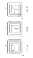
図1は、巻き数3と4分の1の、正方形の平坦な平面状スパイラルとして構成された、中央で給電される両面プリント基板共鳴誘導ワイヤレス電力伝送コイルを含む非自己共振コイル構造を表したものである。実施形態の諸例において、このワイヤレス電力伝送コイルは、少なくとも2回巻きである。図1Aは、4つの独立した導体から成る上面導体パターン100を示したものであるが、2若しくはそれ以上の独立した導体を使用することができる。図1Bは、当該プリント基板を透かして見た底面導体パターン101を示したものである。前記底面導体パターン101は、前記上面導体パターンを垂直な中心線に沿って左から右に反転して90度時計回りに回転したものと同じである。前記導体パターン100、101は、反転させた同一のものである必要はないことが理解されるであろう。ただし、前記上面導体パターン100および底面導体パターン101は、各パターンにより生成される磁束を互いに強化して磁束生成を最大限に高めるよう、十分位置合わせすべきである。図1Cは、上面および底面パターンを重ね合わせたもの102を示している。めっきスルーホール103(一般にビアとしても知られる)は、前記上面100および底部101のトレースパターンを電気接続できる。コイル端子とそれに伴うめっきスルーホール104は、当該コイル102の中央に示されている。基板外の構成要素、例えばコイル共振キャパシタ(コンデンサ)への接続は、複数の並列で独立した導体により行われ、これにより有益な複数の独立した平面状導体構造が延長される。自己共振コイルの場合、端子104は電源に直接接続され、非自己共振コイルにおいて端子は前記共振キャパシタに接続する。また、代替実施形態において、前記上面および底面の層100、101間の接続は、前記めっきスルーホール103の代わりに、電気的構造、例えばクランプ、ラグ、または端子として実装できる。
FIG. 1 represents a non-self-resonant coil structure containing a centrally powered double-sided printed circuit board resonance-guided wireless power transfer coil configured as a square flat planar spiral with three and a quarter turns. It is a thing. In the embodiments of the embodiment, the wireless power transfer coil is wound at least twice. FIG. 1A shows a
図1Cに示したように、上面の導体は、可能な場合、それに対応した底面の導体の上方に直接配置され、そのような配置により均一な磁束伝送が可能になり、前記上面および底面の巻線が同じ磁束分布を捉える。その結果、2つの層および6と2分の1の合計巻き数を有する対称的で平坦なスパイラルインダクタ102が得られる。前記上面100および前記底面101の部分の電流は同じ方向に流れるため、前記上面および底面の層により生成される磁束は強化される。この例では、前記上面導体層の端子104に電流が供給されると、電流は、基板を上から見て時計回りの方向になる。前記底面導体層の端子104に供給される電流は、結果として反時計回りの電流になる。前記上面および底面のスパイラルを接続すると、巻き数が2倍になり、総インダクタンスが4倍に増加する。
As shown in FIG. 1C, the top surface conductors, if possible, are placed directly above the corresponding bottom surface conductors, such placement allows for uniform magnetic flux transmission and winding of the top and bottom surfaces. The lines capture the same magnetic flux distribution. The result is a symmetric,
図2は、巻き数3と4分の1の、正方形の平坦な平面状スパイラルとして構成された、外縁部で給電される両面プリント基板共鳴誘導ワイヤレス電力伝送コイルを含む非自己共振コイル構造の例である。実施形態の諸例において、このワイヤレス電力伝送コイルは、少なくとも2回巻きである。図2Aは、4つの独立した導体から成る上面導体パターン200を示したものであるが、2若しくはそれ以上の独立した導体を使用することができる。図2Bは、当該プリント基板を透かして見た底面導体パターン201を示したものである。前記底面導体パターン201は、前記上面導体パターンを垂直な中心線に沿って左から右に反転して90度時計回りに回転したものと同じである。前記導体パターン200、201は、反転させた同一のものである必要はないことが理解されるであろう。図2Cは、上面および底面パターンを重ね合わせたもの202を示している。めっきスルーホール103(一般にビアとしても知られる)は、前記上面200および底部201のトレースパターンを電気接続できる。コイル端子とそれに伴うめっきスルーホール103は、当該コイル202の外側のコーナーに示されている。基板外の構成要素、例えばコイル共振キャパシタへの接続は、複数の並列で独立した導体104により行われ、これにより有益な複数の独立した平面状導体構造が延長される。自己共振コイルの場合、端子104は電源に直接接続され、非自己共振コイルにおいて端子は前記共振キャパシタに接続する。また、前記上面および底面の層間の接続は、前記めっきスルーホール103の代わりに、電気的構造、例えばクランプ、ラグ、または端子として実装できる。
FIG. 2 shows an example of a non-self-resonant coil structure including a double-sided printed circuit board resonance-guided wireless power transfer coil powered at the outer edge, configured as a square flat planar spiral with three and a quarter turns. Is. In the embodiments of the embodiment, the wireless power transfer coil is wound at least twice. FIG. 2A shows a
図2Cに示したように、上面の導体200は、可能な場合、それに対応した底面の導体201の上方に直接配置され、そのような配置により均一な磁束伝送が可能になり、前記上面および底面の巻線が同じ磁束分布を捉える。その結果、2つの層および6と2分の1の合計巻き数を有する対称的で平坦なスパイラルインダクタ202が得られる。前記上面200および前記底面201の部分の電流は同じ方向に流れるため、前記上面および底面の層により生成される磁束は強化される。この例では、前記上面導体層の端子104に電流が供給されると、電流は、基板を上から見て反時計回りの方向になる。前記底面導体層の端子104に供給される電流は、結果として時計回りの電流になる。前記上面および底面のスパイラルを接続すると、巻き数が2倍になり、総インダクタンスが4倍に増加する。
As shown in FIG. 2C, the
図1および2の実施形態において、単一の巻線導体を構成するよう並列に動作するトレースの数は、動作周波数、トレース材料の導電率、および動作電流により決定される。トレース幅が狭いと、トレース幅の寸法内における導体の渦電流が制限され、個々のトレースの断面全体にわたる均一な電流密度の維持も制限される。均一な磁場における導電素子の渦電流損失は、 In the embodiments of FIGS. 1 and 2, the number of traces operating in parallel to form a single winding conductor is determined by the operating frequency, the conductivity of the trace material, and the operating current. Narrow trace widths limit the eddy currents of the conductor within the dimensions of the trace width and also limit the maintenance of uniform current densities across the cross section of individual traces. The eddy current loss of the conductive element in a uniform magnetic field is

トレースの厚さはAC抵抗に寄与するため、動作周波数における表皮深さにより制約される。一般的な共鳴誘導ワイヤレス電力周波数での表皮深さδは、 The thickness of the trace contributes to the AC resistance and is therefore constrained by the depth of the skin at the operating frequency. The skin depth δ at a typical resonance-induced wireless power frequency is

並列トレースの数は、動作電流、ならびに指定されたトレース断面積および環境条件に関するトレースの電流容量により決定される。図1および2は、4つの並列導体を使った実施形態を示しているが、いかなる数を使用してもよい。巻線全体内の隣接しあうトレース間の分離距離は小さくてよく、同じ巻線全体内においてトレースとそれに隣接するトレース間の電圧はゼロに近いため、プリント基板の製造設計ルールだけに制限される。導体全体間の巻線間の間隔は、隣接しあう巻線間に十分な電圧絶縁性を提供する上で十分なものでなければならない。巻線間の電圧は、巻線の直径同士の比に比例する。プリント基板の誘電層の厚さは、絶縁破壊を防ぐ上で十分でなければならない。 The number of parallel traces is determined by the operating current and the current capacity of the traces for the specified trace cross-sectional area and environmental conditions. Although FIGS. 1 and 2 show an embodiment using four parallel conductors, any number may be used. The separation distance between adjacent traces within the entire winding can be small, and the voltage between a trace and its adjacent traces within the entire winding is close to zero, limiting itself to printed circuit board manufacturing design rules. .. The spacing between the windings across the conductors must be sufficient to provide sufficient voltage insulation between the adjacent windings. The voltage between the windings is proportional to the ratio of the diameters of the windings. The thickness of the dielectric layer of the printed circuit board must be sufficient to prevent dielectric breakdown.
前記上面導体パターン200のより長い外側の導体は、前記底面導体パターン201のより短い内側の導体に接続される。このように導体を内側から外側に切り替えることにより、導体の長さおよびインダクタンスが均一化される。長さとインダクタンスが均一化されることにより、抵抗とリアクタンスが均一化され、導体間の電流分布が均一化される。上面および底側の導体は重ね合わされる。磁束は、導体間の間隙を貫流する。実施形態の例では、すべての導体トレースの長さが等しい。
The longer outer conductor of the
後述するように、図1および2に示した2層構造は、2n層に拡張でき、ここで、nは任意の正の整数である。その2nコイル構造は、自己共振周波数が As will be described later, the two-layer structure shown in FIGS. 1 and 2 can be extended to 2n layers, where n is an arbitrary positive integer. The 2n coil structure has a self-resonant frequency.

図3は、多層多導体ペアの縁部終端コイルを表したものである。この実施形態例において、図3は、それぞれ約3と4分の1~約3と2分の1巻きの個々のコイルを8層スタック(積層)したものを示している。導体パターン300は上面層(層1)、導体パターン301は層2、導体パターン302は層3、導体パターン303は層4、導体パターン304は層5、導体パターン305は層6、導体パターン306は層7、導体パターン307は底面層(層8)である。導体ペア300および301、302および303、304および305、306および307は、図2に示したものと同じ基準に従う。時計回りの電流構成用に、図3A、3C、3E、および3Gのコイル端子104は、入力信号を受信し、図3B、3D、3F、および3Hのコイル端子104は、出力信号を提供する。めっきスルーホール103は、ブラインドビアおよび/またはベリードビアを有して、コイル構成に応じて一定の層を接続するとともに他の層を単離することができる。前記めっきスルーホール103は、すべてが直接互いの上方に位置する必要はないことが理解されるであろう。個々の接続ペアは、独立しためっきスルーホール103パターンとオフセットすることができる。オフセットされためっきスルーホール103を示す一実施形態例を、図3Jに示す。
FIG. 3 shows an edge termination coil of a multi-layered multi-conductor pair. In this embodiment, FIG. 3 shows an 8-layer stack of individual coils with about 3 and 1/4 to about 3 and 1/2 turns, respectively. The
図3Iは、前記複合8層スタックのプリント基板または積層アセンブリを上面から透かして見たものである。導体パターン308は、パターン300~307の重ね合わせである。この実施形態において、めっきスルーホール103は層間で電流を通過させる。コイル端子104は、すべて当該コイルアセンブリの外縁部にある。代替実施形態では、前記コイル構造の中央に開口部が設けられて、導電クランプ機構により、電流が層ペア間を通過できるようにする。
FIG. 3I is a top view of the printed circuit board or laminated assembly of the composite 8-layer stack. The
当業者であれば、図3の前記コイルスタックは、プリント基板(PCB)として実装可能な多層積層されたアセンブリに内設できることが理解されるであろう。 Those skilled in the art will appreciate that the coil stack of FIG. 3 can be installed internally in a multi-layered assembly mountable as a printed circuit board (PCB).
図4は、2nの層を有する多層コイルスタックの4つの例の断面図であり、ここで、「n」は任意の正の整数である。図1、2および3に示した導体パターンは、この図4に示した断面に適用することができる。 FIG. 4 is a cross-sectional view of four examples of a multi-layer coil stack with 2n layers, where "n" is any positive integer. The conductor patterns shown in FIGS. 1, 2 and 3 can be applied to the cross section shown in FIG.
図4Aは、基本的な2層の場合を示しており(n=1)、この場合、400は順電流経路導体、401はリターン電流経路導体、および402は差動モード誘電体である。 FIG. 4A shows the case of two basic layers (n = 1), where 400 is a forward current path conductor, 401 is a return current path conductor, and 402 is a differential mode dielectric.
図4Bは、前記基本的な2層の場合を示しており(n=2)、この場合も、400は順電流経路導体、401はリターン電流経路導体、および402は差動モード誘電体である。この図4Bの実施形態は、本質的に、図4Aに示した2層パネルを2つスタックしたもので、その間に付加的な差動モード誘電層402がある。この実施態様は、交流の順電流およびリターン電流経路導体を含む。図4Bを6層若しくはそれ以上(n=3+)に拡張するため、差動モード誘電体402と、順電流経路導体400と、差動モード誘電体402と、リターン電流経路導体401とを含むパターン404が繰り返される。
FIG. 4B shows the case of the basic two layers (n = 2), in which
図4Cは、基本的な4層の場合を示しており(n=2)、この場合も、400は順電流経路導体、401はリターン電流経路導体、402は差動モード誘電体、そして403はコモンモード誘電層である。この構成は図4Bと同様であるが、順電流が前記上面および底面の層400に流れ、リターン電流が前記内層401に流れるよう、底部の2層が逆転している点で異なる。この結果、前記リターン電流経路導体401が互いに電気的に並列になるため、コモンモード誘電体403が設けられる。図4Cを6層若しくはそれ以上(n=3+)に拡張するため、コモンモード誘電体403と、順電流経路導体400(n=奇数の場合)またはリターン電流経路導体401(n=偶数の場合)のどちらか一方と、差動モード誘電体402と、およびリターン電流経路導体401(n=奇数の場合)または順電流経路導体400(n=偶数の場合)のどちらか一方とを含むパターン405が繰り返される。
FIG. 4C shows the case of a basic four layer (n = 2), where again 400 is a forward current path conductor, 401 is a return current path conductor, 402 is a differential mode dielectric, and 403 is. It is a common mode dielectric layer. This configuration is the same as in FIG. 4B, except that the two bottom layers are reversed so that the forward current flows through the top and
図4Dは、前記基本的な4層の場合を示しており(n=2)、この場合も、400は順電流経路導体、401はリターン電流経路導体、402は差動モード誘電体、そして403はコモンモード誘電層である。この構成は図4Aと同様であるが、前記上面および底面の層が、それぞれ順電流および逆電流を流すため平行に付加された追加層を有する点で異なる。この結果、前記上面の2つの導体400と前記底面の2つの導体401との間にコモンモード誘電体403、およびこの4層スタック中央に1つの差動モード誘電体402が設けられる。図4Dを6層若しくはそれ以上(n=3+)に拡張するため、上面では、コモンモード誘電体403と、順電流経路導体400とを含むパターン406が繰り返される。また、底面では、コモンモード誘電体403と、逆電流経路導体401とを含むパターン407が繰り返される。
FIG. 4D shows the case of the basic four layers (n = 2), again in which 400 is a forward current path conductor, 401 is a return current path conductor, 402 is a differential mode dielectric, and 403. Is a common mode dielectric layer. This configuration is similar to FIG. 4A, except that the top and bottom layers have additional layers added in parallel to carry forward and reverse currents, respectively. As a result, a
図4A~4Dの前記コイル構成を使うと、より多くのコイル層を伴う他の実施形態を作製できることが理解されるであろう。例えば、6つの差動ペアのコイルアセンブリを、図4B、4C,および4Dに示した4層スタックの複数のインスタンスおよび組合せとして実装し、24層コイル設計を提供することができる。 It will be appreciated that the coil configurations of FIGS. 4A-4D can be used to make other embodiments with more coil layers. For example, six differential pairs of coil assemblies can be implemented as multiple instances and combinations of the four-layer stack shown in FIGS. 4B, 4C, and 4D to provide a 24-layer coil design.
図5は、図1~4に示した複数の独立した多層コイル実施態様で構築できるコイルスタックの斜視図である。 FIG. 5 is a perspective view of a coil stack that can be constructed by the plurality of independent multilayer coil embodiments shown in FIGS. 1 to 4.
図5Aは、図1~4に示した複数の独立した多層コイル実施態様で構築できる縁部終端コイルスタックを物理的に表したものである。図5Aの実施形態例では、図3の前記導体パターンを実装した4つの独立な平面状コイルが提供される。アイテム500は、n層の導体パターン300および301を含む平面状コイルであり、ここで、nは正の整数である。アイテム501は、n層の導体パターン302および303を含む平面状コイルである。アイテム502は、n層の導体パターン304および305を含む平面状コイルである。アイテム503は、n層の導体パターン306および307を含む平面状コイルである。コイル端子504は、平面状コイル500~503の独立した「タブ」として実装でき、図示したように前記縁部に沿ってオフセットすることで、独立した端子ペアへの接続を容易にする。信号は、図1~4で例示した実施形態のように、前記基板をその中央を通じて接続するビアまたは端子を使って層間で送信できる。図5Aの実施形態では、前記縁部から内側へスパイラルする縁部パターンが提供され、前記基板は、それら各基板の中央を通じて前記基板を接続するビアまたは端子(図示せず)を通じて信号を送信する。
FIG. 5A physically represents an edge-terminated coil stack that can be constructed in the plurality of independent multilayer coil embodiments shown in FIGS. 1 to 4. In the embodiment of FIG. 5A, four independent planar coils are provided that implement the conductor pattern of FIG.
図5Bは、図1~4に示した複数の独立した多層コイル実施態様で構築できる中央給電コイルスタックを物理的に表したものである。1-4. 図5Bの実施形態例では、図3の前記導体パターンを実装した4つの独立な平面状コイルが提供される。アイテム500は、n層の導体パターン300および301を含む平面状コイルであり、ここで、nは正の整数である。アイテム501は、n層の導体パターン302および303を含む平面状コイルである。アイテム502は、n層の導体パターン304および305を含む平面状コイルである。アイテム503は、n層の導体パターン306および307を含む平面状コイルである。コイル端子504は、平面状コイル500~503の独立した「タブ」として実装でき、図示したように前記中央コアに沿ってオフセットすることで、独立した端子ペアへの接続を容易にする。信号は、図1~4で例示した実施形態のように、前記基板をその中央を通じて接続するビアまたは端子を使って層間で送信できる。図5Bの実施形態では、前記中央から外側へスパイラルする中央給電パターンが提供され、前記基板は、それら各基板の外側のコーナーを通じて前記基板を接続するビアまたは端子(図示せず)を通じて信号を送信する。
FIG. 5B physically represents a central feeding coil stack that can be constructed in the plurality of independent multilayer coil embodiments shown in FIGS. 1 to 4. 1-4. In the embodiment of FIG. 5B, four independent planar coils are provided that implement the conductor pattern of FIG.
図5Cは、縁部終端部および中央終端部の双方を有するコイルスタックを物理的に表したものである。各コイルスタックは、図1~4に示したように、複数の独立した多層コイル実施態様で構築できる。図5Cの実施形態例では、図3の前記導体パターンを実装した4つの独立な平面状コイルが提供される。アイテム500は、n層の導体パターン300および301を含む平面状コイルであり、ここで、nは正の整数である。アイテム501は、n層の導体パターン302および303を含む平面状コイルである。アイテム502は、n層の導体パターン304および305を含む平面状コイルである。アイテム503は、n層の導体パターン306および307を含む平面状コイルである。コイル端子504は、平面状コイル500~503の独立した「タブ」として実装でき、図示したように前記縁部に沿って、ならびに前記中央コアに沿ってオフセットすることで、独立した端子ペアへの接続を容易にする。信号は、図1~4で例示した実施形態のように、前記基板をその中央を通じて接続するビアまたは端子を使って層間で送信できる。図5Cの実施形態では、縁部端子および中央端子の双方を有することにより、縁部給電または中央給電コイルスタックのどちらか一方になるよう前記コイルスタックを構成することができる。
FIG. 5C physically represents a coil stack having both edge and center terminations. Each coil stack can be constructed in a plurality of independent multilayer coil embodiments as shown in FIGS. 1 to 4. In the embodiment of FIG. 5C, four independent planar coils are provided that implement the conductor pattern of FIG.
図5に例示したように複数の独立した多層コイルスタックを利用すると、コイル導体層の総数が大きい場合、製造において費用対効果が得られる。16~24層のプリント基板を1枚製造するよりも、例えば、4~6個の4層コイルスタックを1つのアセンブリへと一体化することができる。付加的な実施形態には「m」個のコイルスタックを含めることができ、ここで、「m」は1より大きい任意の正の整数である(例えば、2つのタブを伴う2つのコイルスタックまたは10のタブを伴う10のコイルスタック)。 Utilizing a plurality of independent multilayer coil stacks as illustrated in FIG. 5 is cost effective in manufacturing when the total number of coil conductor layers is large. Rather than manufacturing one 16-24 layer printed circuit board, for example, 4-6 4-layer coil stacks can be integrated into one assembly. Additional embodiments may include "m" coil stacks, where "m" is any positive integer greater than 1 (eg, two coil stacks with two tabs or 10 coil stacks with 10 tabs).
図6は、図4に示した前記多層平面状コイルスタックの電気的形態である。図6A、6B、6C、6D、および6Iは、終端処理されておらず、したがって層間に直接的な電気接続を有さず、一方、図6E、6F、6G、6H、および6Jは、終端処理されており、構成に応じて層間に直列接続および/または並列接続を有する。 FIG. 6 is an electrical form of the multilayer planar coil stack shown in FIG. FIGS. 6A, 6B, 6C, 6D, and 6I are not terminated and therefore have no direct electrical connection between the layers, while FIGS. 6E, 6F, 6G, 6H, and 6J are terminated. It has a series connection and / or a parallel connection between layers depending on the configuration.
図6Aは、図4Aに示した断面を伴う2層コイルを分布定数素子で表したものである。順電流経路誘導素子600およびリターン電流経路誘導素子601は、前記順電流経路導体400およびリターン経路導体401に対応する。差動モード誘電容量素子602は、前記差動モード誘電体402に対応する。前記コイルの電気端子は603で示す。
FIG. 6A is a two-layer coil with a cross section shown in FIG. 4A represented by a distributed constant element. The forward current
図6Bは、図4Bに示した断面を伴う4層コイルシナリオを分布定数素子で表したものである。順電流経路誘導素子600、リターン電流経路誘導素子601、および差動モード誘電容量素子602は、それぞれ400、401、および402に対応する。前記コイルの電気端子は603で示す。
FIG. 6B represents a four-layer coil scenario with a cross section shown in FIG. 4B with a distributed constant element. The forward current
図6Cは、図4Cに示した断面を伴う4層コイルシナリオを分布定数素子で表したものである。順電流経路誘導素子600、リターン電流経路誘導素子601、および差動モード誘電容量素子602は、それぞれ400、401、および402に対応する。前記コイルの電気端子は603で示す。この構成は図6Bと同様であるが、順電流が前記上面および底面の層600に流れ、リターン電流が前記内層601に流れるよう、底部の2層が逆転している点で異なる。この結果、コモンモード誘電容量素子604は、前記コモンモード誘電体403に対応する。
FIG. 6C represents a four-layer coil scenario with a cross section shown in FIG. 4C with a distributed constant element. The forward current
図6Dは、図4Dに示した断面を伴う4層コイルシナリオを分布定数素子で表したものである。この構成は図6Aと同様であるが、前記上面および底面の層が、それぞれ順電流および逆電流を流すため平行に付加された追加層を有する点で異なる。順電流経路誘導素子600、リターン電流経路誘導素子601、および差動モード誘電容量素子602は、それぞれ400、401、および402に対応する。前記コイルの電気端子は603で示す。前記コモンモード誘電容量素子は604で示す。
FIG. 6D represents a four-layer coil scenario with a cross section shown in FIG. 4D with a distributed constant element. This configuration is similar to FIG. 6A, except that the top and bottom layers have additional layers added in parallel to carry forward and reverse currents, respectively. The forward current
図6E、6F、6G、および6Hは、それぞれ図6A、6B、6C、および6Dと同一であるが、平面状コイル層が、順電流経路およびリターン電流経路誘導素子の直列接続605で相互接続されている点で異なる。任意選択的に、図6Fおよび6Gの中間2層を、破線のコネクタ606で示すように接続することもできる。電気的に、接続部606は不要だが、製造上の利点をもたらす。
6E, 6F, 6G, and 6H are identical to FIGS. 6A, 6B, 6C, and 6D, respectively, but the planar coil layers are interconnected by a
図6Iは、完全に直列共振で端子が2つしかない4層インターリーブコイル構造を分布定数素子で表したものである。この実施形態は、誘導および容量素子が直列LC共振を生じるため、平面状コイル層間にめっきスルーホールを必要としない。 FIG. 6I shows a four-layer interleaved coil structure with completely series resonance and only two terminals by a distributed constant element. This embodiment does not require plating through holes between the planar coil layers because the inductive and capacitive elements cause series LC resonance.
図6Jは、完全に並列共振で端子が2つしかない4層インターリーブコイル構造を分布定数素子で表したものである。この実施形態では、前記誘導素子を層1から層2へ、層3へ、そして層4へと直列に接続するめっきスルーホールを実装していない。この構造の結果、前記直列誘導素子および前記コイル巻線間の並列容量から並列共振が生じる。 FIG. 6J shows a four-layer interleaved coil structure having completely parallel resonance and having only two terminals by a distributed constant element. In this embodiment, the plating through holes that connect the inductive element in series from layer 1, layer 2, layer 3, and layer 4 are not mounted. As a result of this structure, parallel resonance occurs from the parallel capacitance between the series induction element and the coil winding.
図7は、一実施形態例に係る車両側の伝送コイルアセンブリ700の断面を表したものである。この伝送コイルアセンブリ700は、コイルアセンブリカバー701およびコイルアセンブリ筐体702を含む環境的にシールされた筐体内に収容される。図1A~1Cの前記コイル導体を含むプリント基板は、703で示す。コイル導体703の直接上方には、フェライトバーまたはタイルを単一アセンブリとして一体的に保持するフェライトに接合されたフェライト裏打ち層704、非導電接着シート、テープ、フィルム、または布がある。磁束密度は、当該コイルアセンブリの中央で最強になる。フェライト層の空間密度およびフェライトの厚さは、飽和を防ぐうえで十分なものでなければならない。磁束強度は前記コイル外周へ向かって減少するため、フェライト層の空間密度および/または厚さを薄くしながら飽和を回避できる。フェライト層の薄層化は、伝送コイルの重量とコストを軽減する手段として望ましい。一実施形態例において、フェライト層705は、一定の厚さを有するフェライトバーまたはプレートのアレイとして実装される。前記アレイのタイルは、前記コイルの中央で継続的または略継続的である。タイルの密度は、外周に近づくとともに漸減される。このフェライト層のタイルは、必要に応じて間隙を有することにより、コイル端子導体その他の突起または貫通を必要に応じて可能にする。
FIG. 7 shows a cross section of the
一実施形態例において、前記フェライトバータイル705およびフェライト裏打ち層704は、フェライト粉末を結合剤、例えば熱可塑性物質または樹脂、および可能性として追加物質、例えば熱伝導性を改善する導熱性の電気絶縁粉末と混合したものを含む単一複合磁気構造で置き換えられ、その単一複合磁気構造は、最終形態または略最終形態へと射出成形または成形される。磁束は、前記伝送コイル703の中央で最も強くなり、外周へ向かって減少する。これは、前記複合フェライト層705を、磁束が最も強くなる中央ではより厚くすることでフェライト材料の飽和を回避し、外周ではより薄くすることで重量と材料コストを削減できることを意味する。材料組成を空間的に変化させると、位置の関数として熱および磁気特性をカスタマイズできる。冷却液用の流路は、必要な場所に必要に応じて含めることができる。
In one embodiment, the ferrite bartile 705 and the
渦電流シールド706は、前記フェライト層705で方向転換されなかった残留磁束を捉え散逸させる導電性のシートまたは層として実装される。渦電流シールド706は、当該伝送コイルアセンブリ700に構造的強度をもたらす金属製プレートであってよい。この用途には、比透磁率が1に近い非鉄金属が、前記フェライト層705の磁束操作の撹乱を防ぐうえで好適である。あるいは、前記渦電流シールド706は、誘電体基板上に成膜した導電フィルムであってよい。また、前記渦電流シールド706は、前記渦電流シールド706を前記筐体702内面に合着し、または前記筐体をアルミニウムで作製することにより、前記コイルアセンブリ筐体内に一体化できる。
The
層707は、機械的に適合性の高い非導電層であり、前記導体プリント基板703および前記フェライト磁束操作層705用に、熱伝導性および物理的な離間により機械的支持、除熱をもたらす。前記フェライト磁束操作層705は、前記導体プリント基板703または前記渦電流シールド706に接触または略接触してはならず、これは、前者については過度の近接効果による抵抗損失を防ぐためで、後者については過度の渦電流損失を防ぐためである。前記離間層707は、発熱する回路と除熱面間の間隙充填剤として使用される従来の弾性圧縮パッドで作製できる。あるいは、離間層707は、熱伝導性の液体、例えば鉱物油とともに注入されたオープンセル(連通気泡)発泡材として実装できる。前記離間層707に必要に応じて穴またはスロットを設けると、冷却液流が改善される。前記導体プリント基板703には、導体の連続性を保つため、導体トレース間または巻線間にスロットが設けられる。前記コイルアセンブリ筐体701は、他のシステム構成要素、例えば共振キャパシタ、整流器、整流後リップルフィルター構成要素、制御部、通信部、異物および生物検出回路、およびインターフェース電子機器を収容する別個の閉鎖容積708を含むこともできる。
The
図7において、前記プリント基板703は、上面および底面の両面に導電トレースを備えているが、中間層は有していない。複数のプリント基板または多層プリント基板は、並列に接続された巻線と併用して電流容量を高め、または直列に接続された巻線と併用してインダクタンスを高めることができる。
In FIG. 7, the printed
図8は、代替実施形態に係る車両側の伝送コイルアセンブリ800の断面を表したものである。付加的なプリント基板または層を必要に応じて含めると、伝送コイルの位置合わせ、近距離無線通信、異物・生物検出、または電場のファラデーシールド機能を実施できる。共振キャパシタは、表面実装キャパシタのアレイ、容量の増加を可能にする複数のキャパシタ、および定格電圧を含むプリント基板として実装できる。あるいは、前記共振キャパシタは前記フェライト層705と前記コイルアセンブリ筐体702間に位置する追加層として実装された薄い多層の金属化した誘電体シートとして物理的に実現できる。図8では、物体検出PCB 809と、フェライト絶縁層810と、通信PCB 811とが、前記導体プリント基板703と前記コイルアセンブリカバー702との間に示されている。前記コイルアセンブリ筐体702は、他のシステム構成要素、例えば共振キャパシタ、整流器、整流後リップルフィルター構成要素、制御部、通信部、異物および生物検出回路、およびインターフェース電子機器を収容する別個の閉鎖容積708を含むことができる。さらに別の実施形態において、共振キャパシタは、前記伝送コイルアセンブリ800内で前記フェライト層705の場の強度が低い側に位置する薄い大面積の金属化した誘電体フィルムとして実現できる。
FIG. 8 shows a cross section of the
一代替実施形態では、導電テープまたはストリップ(帯状体)の平坦なスパイラルで、前記プリント基板703を置き換える。前記テープまたはストリップは、前記導体面を横切る渦電流を最小限に抑えるため、その幅の次元が入射磁束と平行になるよう配置される。厚さ次元での渦電流を最小化するため、前記導電テープまたはストリップの厚さは、動作周波数における前記トレース導体の表皮深さの4倍よりも厚くならないよう制限される。非導電性スペーサーにより、隣接しあうスパイラル巻線間の分離間隔を保つ。あるいは、除熱を妨げないよう、前記導電テープまたはストリップ導体は絶縁されない。テープまたはストリップの幅を広げると、導体の電流容量が増す。テープまたはストリップのスパイラルを垂直にスタックすると、プリント回路導体が並列に配線されている場合は電流容量を高めることができ、直列に配線されている場合はインダクタンスを高めることができる。
In one alternative embodiment, the printed
当業者であれば、接地側の伝送コイル層を車両側のコイルと同一にすると、製造効率を改善できることが理解されるであろう。図9は、センサー開口部900を加えた車両伝送コイルアセンブリの実施形態例である。センサー電子機器901は開口部導管902内を調べ、その開口部導管902は、センサー導管エンドキャップ903により終端する。
Those skilled in the art will appreciate that manufacturing efficiency can be improved by making the grounded transmission coil layer the same as the vehicle side coil. FIG. 9 is an example of an embodiment of a vehicle transmission coil assembly to which a
市販の共鳴誘導ワイヤレス電源機器は、通常、電流の、および予測される法規制要件を満たす補助システムを必要とする。これらの補助システムは、コイル位置合わせエラー検出、通信、異物検出、および生物検出の機能を含み、これらは、すべて前記伝送コイル作動面の幾何学的中心に設置するのが最適である。ただし、前記作動面の中心は磁束振幅が高いため、配線および電子回路をその位置にすることはできない。 Commercially available resonant induction wireless power supply devices typically require auxiliary systems that meet current and expected regulatory requirements. These auxiliary systems include coil alignment error detection, communication, foreign body detection, and biological detection functions, all of which are best placed at the geometric center of the transmission coil working surface. However, since the magnetic flux amplitude is high at the center of the working surface, the wiring and the electronic circuit cannot be placed at that position.
図9は、これまでに図7で示した伝送コイルアセンブリ700を示したもので、その中央にはセンサー開口部900が備えられている。前記伝送コイルアセンブリの厚さ寸法を貫通するこの開口部900は、この伝送コイルアセンブリの高磁束強度前面から、前記筐体容積708内部の低磁束強度領域への、前記センサーまたは通信信号の双方向通信を可能にする。前記筐体容積708内の前記センサー電子機器は、光学、光学画像、光学動画、超音波のほか、マイクロ波、ミリメートル波(ミリ波)、またはテラヘルツ波の電磁エネルギーを利用できる。902および903で示した構成要素は、それぞれ前記開口部導管および開口部エンドキャップである。前記開口部導管およびエンドキャップの内設は、センサーのモダリティに応じて異なる。光センサーおよび光通信の場合、前記導管は、非導電性の中空管、透明なライトパイプ、または空間的にコヒーレントまたは非コヒーレントな光ファイバーバンドルとすることができる。前記エンドキャップ903は、前記伝送コイルカバー702とともに対環境シール(environmental seal)を提供するが、光学レンズ、例えば広角または魚眼レンズを含むこともできる。前記導管902は、光学部品、例えばレンズも含むことができる。渦電流の発生を防ぐには、非導電材料が好ましい。超音波センサーまたは通信モダリティの場合、前記センサー導管は音響導波路である。前記エンドキャップ903は、上記のように対環境シール(environmental seal)を提供し、音響レンズまたはディフューザーを含むことができる。
FIG. 9 shows the
電磁センサーモダリティの場合、前記センサー導体は、電磁波導波路または伝送線路構造である。従来の金属製導波路または伝送線路構造、例えばストリップライン伝送線路は、強磁場で渦電流が生じるため適さない。そのような構造は、従来の導波路または伝送線路構造に存在する連続的な金属表面をハイパスまたはバンドパス周波数選択的な表面で置き換えることにより、適切なものにできる。あるいは、前記導管伝送線路は、前記フェライト層の低磁気強度側にランチャーを伴う、または連続的な金属表面に代えて周波数選択性で構成されたランチャーを伴うグーボー単線伝送線路として実装することができる。一実施形態例において、前記電磁波導波路は、比誘電率の高いコアが比誘電率の低い媒体に囲まれたものを含む従来の誘電体導波路として実装される。前記エンドキャップ903は、誘電体または人工誘電体レンズを含むことのできる対環境シールを提供する。前記巻線層703および小さいフェライトタイルサイズ用にフレキシブルプリント回路基板を使用し、または柔軟な若しくは非平面状の複合フェライト層705を使用すると、機械的な適合性のため、空気力学的または流体力学的な抗力軽減のため、あるいは車体または円筒形その他の非平面形状を有する物体、例えば自律型水中航走体、砲弾、または同様な物体上への配置用に、非平面状の表面、例えば円筒形の形状に合わせた前記伝送コイルアセンブリを作製できる。
In the case of an electromagnetic sensor modality, the sensor conductor is an electromagnetic waveguide or transmission line structure. Conventional metal waveguide or transmission line structures, such as stripline transmission lines, are not suitable because eddy currents are generated in strong magnetic fields. Such structures can be made appropriate by replacing the continuous metal surfaces present in conventional waveguide or transmission line structures with high-pass or band-pass frequency-selective surfaces. Alternatively, the conduit transmission line can be implemented as a goobo single line transmission line with a launcher on the low magnetic strength side of the ferrite layer, or with a launcher configured with frequency selectivity instead of a continuous metal surface. .. In one embodiment, the electromagnetic wave guide is implemented as a conventional dielectric waveguide including a core having a high relative permittivity surrounded by a medium having a low relative permittivity. The
図10は、代替実施形態に係る、センサー開口部が加えられた車両側の伝送コイルアセンブリ800の断面を表したものである。図8の実施形態のように、付加的なプリント基板または層を必要に応じて含めると、伝送コイルの位置合わせ、近距離無線通信、異物・生物検出、または電場のファラデーシールド機能を実施できる。図10では、図8の実施形態のように、物体検出PCB 809と、フェライト絶縁層810と、通信PCB 811とが、前記導体プリント基板703と前記コイルアセンブリカバー702との間に設けられている。
FIG. 10 shows a cross section of the
以上、種々の実施態様について説明したが、これらは単なる例として示したものであり、限定的なものではないことを理解すべきである。例えば、上述したシステムおよび方法に伴う要素(素子)のいずれも、本明細書において上述した任意の望ましい機能を使用することができる。したがって、好適な実施態様の範囲および要旨は、上述した実施態様例のいずれにも限定されるものではない。 Although various embodiments have been described above, it should be understood that these are merely examples and are not limited. For example, any of the elements associated with the systems and methods described above can use any of the desired functions described herein. Therefore, the scope and gist of the preferred embodiments are not limited to any of the embodiments described above.
Claims (14)
2n層コイルスタックであって、当該nは正の数であり、当該コイルスタックの各層は、
第1の側面と第2の側面とを有する誘電体と、
前記誘電体の前記第1の側面上にスパイラル状に巻かれた第1の複数の導体を有する第1の導体パターンと、
前記誘電体の前記第2の側面上にスパイラル状に巻かれた第2の複数の導体を有する第2の導体パターンであって、当該第2の導体パターンが前記第1の導体パターンに位置合わせされることにより、前記第1の導体パターンにより生成される磁束が当該第2の導体パターンにより強化されるものである、前記第2の導体パターンと
を有し、
前記第1および第2の導体パターンは互いに相対的に配置され、それにより同じ方向に磁束が伝送されるものであり、
前記2n層コイルスタックの各層間の容量は、前記2n層コイルスタックが

共鳴誘導ワイヤレス電力伝送コイル。 Resonance induction wireless power transmission coil
In a 2n layer coil stack, the n is a positive number, and each layer of the coil stack is
A dielectric having a first side surface and a second side surface,
A first conductor pattern having a first plurality of conductors spirally wound on the first side surface of the dielectric.
A second conductor pattern having a second plurality of conductors spirally wound on the second side surface of the dielectric, wherein the second conductor pattern is aligned with the first conductor pattern. By doing so, the magnetic flux generated by the first conductor pattern is enhanced by the second conductor pattern, and has the second conductor pattern.
The first and second conductor patterns are arranged relative to each other, whereby magnetic flux is transmitted in the same direction.
The capacitance between each layer of the 2n layer coil stack is determined by the 2n layer coil stack.
Resonance induction wireless power transfer coil.
前記プリント基板を貫通する少なくとも1つのオフセットされためっきスルーホールを有し、これにより、前記第1および第2の導体パターンの各導体が電気接続されるものである、共鳴誘導ワイヤレス電力伝送コイル。 In the resonance induction wireless power transmission coil according to claim 1, the dielectric has a printed circuit board, and the resonance induction wireless power transmission coil further comprises a printed circuit board.
A resonance induction wireless power transfer coil having at least one offset plated through hole penetrating the printed circuit board, whereby each conductor of the first and second conductor patterns is electrically connected.
クランプ、ラグ、および端子のうち少なくとも1つを有する少なくとも1つの電気接続部を有するものである、共鳴誘導ワイヤレス電力伝送コイル。 In the resonance induction wireless power transmission coil according to claim 1, further
A resonant inductive wireless power transfer coil that has at least one electrical connection with at least one of a clamp, a lug, and a terminal.
前記第1および第2の導体パターンの中央部、または前記第1および第2の導体パターンの外縁部および前記プリント基板の外縁部にコイル端子とそれに伴うスルーホールを有するものである、共鳴誘導ワイヤレス電力伝送コイル。 In the resonance induction wireless power transmission coil according to claim 2, further
Resonance-induced wireless having coil terminals and associated through-holes at the center of the first and second conductor patterns, or at the outer edges of the first and second conductor patterns and the outer edges of the printed circuit board. Power transmission coil.
各プリント基板の縁部または中央部に沿ってオフセットされる独立したタブとして実装された端子を有し、これにより各プリント基板の各導体パターンの独立した端子ペアへの接続が容易になるものである、共鳴誘導ワイヤレス電力伝送コイル。 In the resonance induction wireless power transmission coil according to claim 2, further
It has terminals mounted as independent tabs that are offset along the edges or center of each printed circuit board, which facilitates connection to independent terminal pairs of each conductor pattern on each printed circuit board. There is a resonance induction wireless power transmission coil.
各プリント基板の中央部または縁部を通じて各プリント基板を接続するビアまたは第2の端子を有するものである、共鳴誘導ワイヤレス電力伝送コイル。 In the resonance induction wireless power transmission coil according to claim 11, further
A resonance induction wireless power transfer coil having vias or a second terminal connecting each printed circuit board through the center or edge of each printed circuit board.
前記誘電体は平坦なスパイラルが設けられた導電テープを有し、前記第2の導体パターンは、垂直な中心線に沿って左から右へ反転され、90°回転されている点を除いて前記第1の導体パターンと同じであり、この共鳴誘導ワイヤレス電力伝送コイルは、さらに、
前記第1および第2の導体パターンの各導体を電気接続する少なくとも1つの電気接続部を有し、
前記第1および第2の導体パターンは互いに相対的に配置され、それにより同じ方向に磁束が伝送されるものであり、前記導電テープの厚さは、動作周波数における前記第1の導体パターンの表皮深さの4倍の厚さを超えないものであり、ここで、共鳴誘導ワイヤレス電力動作周波数での表皮深さδは、

共鳴誘導ワイヤレス電力伝送コイル。 The resonance induction wireless power transmission coil according to claim 1.
The dielectric has a conductive tape provided with a flat spiral, the second conductor pattern being flipped from left to right along a vertical centerline and rotated by 90 °. Same as the first conductor pattern, this resonant induction wireless power transfer coil further
It has at least one electrical connection that electrically connects each conductor of the first and second conductor patterns.
The first and second conductor patterns are arranged relative to each other so that magnetic flux is transmitted in the same direction, and the thickness of the conductive tape is the skin of the first conductor pattern at the operating frequency. It does not exceed four times the depth, where the skin depth δ at the resonance induced wireless power operating frequency is
Resonance induction wireless power transfer coil.
筐体と、
請求項1または13記載の共鳴誘導ワイヤレス電力伝送コイルと、
フェライト層と、
渦電流シールドと
を有し、
前記共鳴誘導ワイヤレス電力伝送コイル、前記フェライト層、および前記渦電流シールドは、前記筐体内に平行に設けられるものである、
共鳴誘導ワイヤレス電力伝送コイルアセンブリ。 Resonance induction wireless power transfer coil assembly
With the housing
The resonance induction wireless power transmission coil according to claim 1 or 13 .
Ferrite layer and
Has an eddy current shield and
The resonance induction wireless power transmission coil, the ferrite layer, and the eddy current shield are provided in parallel in the housing.
Resonance induction wireless power transfer coil assembly.
Priority Applications (1)
| Application Number | Priority Date | Filing Date | Title |
|---|---|---|---|
| JP2022069788A JP7350382B2 (en) | 2017-05-30 | 2022-04-21 | Wireless power transmission thin coil assembly |
Applications Claiming Priority (3)
| Application Number | Priority Date | Filing Date | Title |
|---|---|---|---|
| US201762512544P | 2017-05-30 | 2017-05-30 | |
| US62/512,544 | 2017-05-30 | ||
| PCT/US2018/035060 WO2018222669A1 (en) | 2017-05-30 | 2018-05-30 | Wireless power transfer thin profile coil assembly |
Related Child Applications (1)
| Application Number | Title | Priority Date | Filing Date |
|---|---|---|---|
| JP2022069788A Division JP7350382B2 (en) | 2017-05-30 | 2022-04-21 | Wireless power transmission thin coil assembly |
Publications (3)
| Publication Number | Publication Date |
|---|---|
| JP2020522885A JP2020522885A (en) | 2020-07-30 |
| JP2020522885A5 JP2020522885A5 (en) | 2021-12-23 |
| JP7082775B2 true JP7082775B2 (en) | 2022-06-09 |
Family
ID=64456463
Family Applications (2)
| Application Number | Title | Priority Date | Filing Date |
|---|---|---|---|
| JP2019565876A Active JP7082775B2 (en) | 2017-05-30 | 2018-05-30 | Wireless power transfer thin coil assembly |
| JP2022069788A Active JP7350382B2 (en) | 2017-05-30 | 2022-04-21 | Wireless power transmission thin coil assembly |
Family Applications After (1)
| Application Number | Title | Priority Date | Filing Date |
|---|---|---|---|
| JP2022069788A Active JP7350382B2 (en) | 2017-05-30 | 2022-04-21 | Wireless power transmission thin coil assembly |
Country Status (9)
| Country | Link |
|---|---|
| US (1) | US20200168393A1 (en) |
| EP (2) | EP3631819B1 (en) |
| JP (2) | JP7082775B2 (en) |
| KR (1) | KR102405652B1 (en) |
| CN (1) | CN110999028B (en) |
| CA (1) | CA3065782A1 (en) |
| ES (1) | ES2964226T3 (en) |
| PT (1) | PT3631819T (en) |
| WO (1) | WO2018222669A1 (en) |
Families Citing this family (19)
| Publication number | Priority date | Publication date | Assignee | Title |
|---|---|---|---|---|
| JP2020027813A (en) * | 2018-08-09 | 2020-02-20 | 矢崎総業株式会社 | Power transmission unit |
| EP3906604A1 (en) * | 2018-12-31 | 2021-11-10 | 3M Innovative Properties Company | Wireless power transfer |
| US20220416583A1 (en) * | 2019-09-26 | 2022-12-29 | Soreq Nuclear Research Center | Wireless enhanced power transfer |
| US11387678B2 (en) | 2019-09-27 | 2022-07-12 | Apple Inc. | Stacked resonant structures for wireless power systems |
| TWI775022B (en) * | 2019-12-16 | 2022-08-21 | 圓凱科技實業股份有限公司 | Wireless charging mat and manufacturing method thereof |
| JP2023517077A (en) * | 2020-03-10 | 2023-04-21 | ティーシー1 エルエルシー | Systems and methods for wireless power transfer to ventricular assist devices |
| US11784503B2 (en) | 2021-02-22 | 2023-10-10 | Inductev Inc. | Passive arc detection and mitigation in wireless power transfer system |
| US11585836B2 (en) | 2020-03-20 | 2023-02-21 | InductEV, Inc. | Current sensing in a wireless power transfer system |
| CN113539636B (en) * | 2020-04-13 | 2022-12-06 | 鹏鼎控股(深圳)股份有限公司 | Wireless charging coil structure and preparation method thereof |
| US11581755B2 (en) | 2020-07-28 | 2023-02-14 | InductEV, Inc. | Efficiency gains through magnetic field management |
| KR102544750B1 (en) * | 2020-12-22 | 2023-06-16 | 주식회사 유라코퍼레이션 | Wireless Charging System |
| CN113192721A (en) * | 2021-01-21 | 2021-07-30 | 龙腾 | Inductance structure based on printed circuit board, flexible multilayer printed circuit board comprising same and transformer structure comprising same |
| DE102021112455A1 (en) * | 2021-05-12 | 2022-11-17 | Technische Universität Dresden, Körperschaft des öffentlichen Rechts | Coil assemblies and method of manufacturing a coil assembly |
| WO2022265469A1 (en) * | 2021-06-18 | 2022-12-22 | 현대자동차주식회사 | Wireless power transmission device comprising coil structure and power transfer circuit for wireless power transmission, and wireless power reception device |
| WO2023081838A1 (en) * | 2021-11-05 | 2023-05-11 | Siemens Healthcare Diagnostics Inc. | Electromagnetic pcb crossroads topologies for automation track systems |
| TWI801302B (en) * | 2022-08-11 | 2023-05-01 | 台灣電力股份有限公司 | Frequency-selective surface structure for wireless power device |
| KR102540173B1 (en) * | 2022-09-14 | 2023-06-07 | 주식회사 스키아 | Breast region segmentation apparatus and method using magnetic resonance images |
| KR20240038433A (en) * | 2022-09-16 | 2024-03-25 | 주식회사 모다이노칩 | Electronic component |
| CN116469654A (en) * | 2023-04-04 | 2023-07-21 | 广东德维斯电子科技有限公司 | Transformer structure and assembly auxiliary assembly part thereof |
Citations (5)
| Publication number | Priority date | Publication date | Assignee | Title |
|---|---|---|---|---|
| WO2012053439A1 (en) | 2010-10-21 | 2012-04-26 | Tdk株式会社 | Coil component and method for producing same |
| WO2013179639A1 (en) | 2012-05-28 | 2013-12-05 | パナソニック株式会社 | Contactless connector system |
| US20150077208A1 (en) | 2013-09-16 | 2015-03-19 | Ken Goldman | High-q parallel-trace planar spiral coil for biomedical implants |
| JP2015528272A (en) | 2012-06-27 | 2015-09-24 | クアルコム,インコーポレイテッド | Electric vehicle wireless charging with duration monitoring of charging operation mode |
| JP2016093088A (en) | 2014-11-01 | 2016-05-23 | パナソニックIpマネジメント株式会社 | Power transmission device, vehicle having the same and radio power transmission system |
Family Cites Families (37)
| Publication number | Priority date | Publication date | Assignee | Title |
|---|---|---|---|---|
| US20030161086A1 (en) * | 2000-07-18 | 2003-08-28 | X2Y Attenuators, Llc | Paired multi-layered dielectric independent passive component architecture resulting in differential and common mode filtering with surge protection in one integrated package |
| US8169185B2 (en) * | 2006-01-31 | 2012-05-01 | Mojo Mobility, Inc. | System and method for inductive charging of portable devices |
| US7973635B2 (en) * | 2007-09-28 | 2011-07-05 | Access Business Group International Llc | Printed circuit board coil |
| US20100261038A1 (en) * | 2007-11-02 | 2010-10-14 | Nobuyoshi Imaoka | Composite magnetic material for magnet and method for manufacturing such material |
| KR20120029433A (en) * | 2009-05-20 | 2012-03-26 | 코닌클리케 필립스 일렉트로닉스 엔.브이. | Electronic device having an inductive receiver coil with ultra-thin shielding layer and method |
| CN103401321B (en) * | 2009-06-25 | 2016-05-25 | 株式会社村田制作所 | Power delivery system and non-contact charging device |
| WO2011001709A1 (en) * | 2009-07-03 | 2011-01-06 | 株式会社村田製作所 | Antenna and antenna module |
| JP5471283B2 (en) * | 2009-10-19 | 2014-04-16 | Tdk株式会社 | Wireless power feeding device, wireless power receiving device, and wireless power transmission system |
| US8901775B2 (en) * | 2010-12-10 | 2014-12-02 | Everheart Systems, Inc. | Implantable wireless power system |
| US20130181668A1 (en) * | 2010-12-01 | 2013-07-18 | Panasonic Corporation | Non-contact charging module and non-contact charging instrument |
| US8970069B2 (en) * | 2011-03-28 | 2015-03-03 | Tdk Corporation | Wireless power receiver and wireless power transmission system |
| US20120274148A1 (en) * | 2011-04-27 | 2012-11-01 | Samsung Electro-Mechanics Co., Ltd. | Contactless power transmission device and electronic device having the same |
| JP2013062386A (en) * | 2011-09-14 | 2013-04-04 | Tokai Rubber Ind Ltd | Non-contact power transmission device |
| US9240270B2 (en) * | 2011-10-07 | 2016-01-19 | Utah State University | Wireless power transfer magnetic couplers |
| US9160205B2 (en) * | 2012-03-20 | 2015-10-13 | Qualcomm Incorporated | Magnetically permeable structures |
| KR101339486B1 (en) * | 2012-03-29 | 2013-12-10 | 삼성전기주식회사 | Thin film coil and electronic device having the same |
| US20140177197A1 (en) * | 2012-12-26 | 2014-06-26 | Nokia Corporation | Multi-Layered Magnetic Shields |
| WO2014130065A1 (en) * | 2013-02-25 | 2014-08-28 | Access Business Group International Llc | Variable pitch spiral coil |
| US9812774B2 (en) * | 2013-03-05 | 2017-11-07 | Amosense Co., Ltd. | Composite sheet for shielding magnetic field and electromagnetic wave, and antenna module comprising same |
| JP6306288B2 (en) * | 2013-05-13 | 2018-04-04 | 日東電工株式会社 | Coil printed wiring board, power receiving module, battery unit and power receiving communication module |
| CN104184217B (en) * | 2013-08-21 | 2016-08-10 | 深圳市安普盛科技有限公司 | Induction coil and manufacture method, wireless charging system for wireless power transmission |
| WO2015064694A1 (en) | 2013-11-01 | 2015-05-07 | 戸田工業株式会社 | Soft magnetic ferrite resin composition, soft magnetic ferrite resin composition molded body, and power transmission device for non-contact power supply system |
| JP6516765B2 (en) * | 2013-11-11 | 2019-05-22 | ティーシー1 エルエルシー | Resonant power transmission coil with hinge |
| US20150303707A1 (en) * | 2014-04-16 | 2015-10-22 | Witricity Corporation | Wireless energy transfer for mobile device applications |
| CN105576847B (en) * | 2014-11-01 | 2018-05-11 | 松下知识产权经营株式会社 | Power transmission device, the vehicle and Wireless power transmission system for being equipped with power transmission device |
| CN107112789B (en) * | 2015-01-12 | 2020-11-03 | 阿莫绿色技术有限公司 | Heat dissipation unit and wireless power transceiver with same |
| US9912172B2 (en) * | 2015-01-14 | 2018-03-06 | Qualcomm Incorporated | Asymmetrically layered stacked coils and/or chamfered ferrite in wireless power transfer applications |
| JP6596942B2 (en) * | 2015-06-04 | 2019-10-30 | 株式会社Ihi | Coil device |
| US10320586B2 (en) * | 2015-07-14 | 2019-06-11 | At&T Intellectual Property I, L.P. | Apparatus and methods for generating non-interfering electromagnetic waves on an insulated transmission medium |
| KR101926594B1 (en) * | 2015-08-20 | 2018-12-10 | 주식회사 아모텍 | Antenna unit for a wireless charging and wireless charging module having the same |
| KR102405414B1 (en) * | 2015-10-13 | 2022-06-07 | 주식회사 위츠 | Magnetic shileding sheet and wireless power transmitting apparatus including the same |
| US9899879B2 (en) * | 2016-02-15 | 2018-02-20 | Motorola Solutions, Inc. | Systems and methods for controlling wireless power transfer |
| JP6743432B2 (en) * | 2016-03-14 | 2020-08-19 | 株式会社Ihi | Coil device |
| US10374467B2 (en) * | 2016-03-30 | 2019-08-06 | Tdk Corporation | Coil unit, wireless power feeding device, wireless power receiving device and wireless power transmission device |
| KR101772871B1 (en) * | 2016-07-11 | 2017-08-30 | 주식회사 두산 | Composite substrate for antenna module and preparation method thereof |
| TW201816539A (en) * | 2016-10-20 | 2018-05-01 | 華碩電腦股份有限公司 | Wireless charging structure and method for forming the same |
| EP3594974B1 (en) * | 2017-03-10 | 2021-09-15 | Mitsubishi Electric Engineering Company, Limited | Resonance-type power transfer coil |
-
2018
- 2018-05-30 US US16/615,290 patent/US20200168393A1/en active Pending
- 2018-05-30 EP EP18810537.3A patent/EP3631819B1/en active Active
- 2018-05-30 CN CN201880035909.7A patent/CN110999028B/en active Active
- 2018-05-30 KR KR1020197038173A patent/KR102405652B1/en active IP Right Grant
- 2018-05-30 WO PCT/US2018/035060 patent/WO2018222669A1/en active Application Filing
- 2018-05-30 ES ES18810537T patent/ES2964226T3/en active Active
- 2018-05-30 CA CA3065782A patent/CA3065782A1/en active Pending
- 2018-05-30 JP JP2019565876A patent/JP7082775B2/en active Active
- 2018-05-30 PT PT188105373T patent/PT3631819T/en unknown
- 2018-05-30 EP EP21203177.7A patent/EP3968346A1/en active Pending
-
2022
- 2022-04-21 JP JP2022069788A patent/JP7350382B2/en active Active
Patent Citations (5)
| Publication number | Priority date | Publication date | Assignee | Title |
|---|---|---|---|---|
| WO2012053439A1 (en) | 2010-10-21 | 2012-04-26 | Tdk株式会社 | Coil component and method for producing same |
| WO2013179639A1 (en) | 2012-05-28 | 2013-12-05 | パナソニック株式会社 | Contactless connector system |
| JP2015528272A (en) | 2012-06-27 | 2015-09-24 | クアルコム,インコーポレイテッド | Electric vehicle wireless charging with duration monitoring of charging operation mode |
| US20150077208A1 (en) | 2013-09-16 | 2015-03-19 | Ken Goldman | High-q parallel-trace planar spiral coil for biomedical implants |
| JP2016093088A (en) | 2014-11-01 | 2016-05-23 | パナソニックIpマネジメント株式会社 | Power transmission device, vehicle having the same and radio power transmission system |
Also Published As
| Publication number | Publication date |
|---|---|
| EP3631819A1 (en) | 2020-04-08 |
| KR20200012916A (en) | 2020-02-05 |
| EP3631819A4 (en) | 2021-06-02 |
| JP2020522885A (en) | 2020-07-30 |
| EP3631819B1 (en) | 2023-10-18 |
| JP7350382B2 (en) | 2023-09-26 |
| EP3968346A1 (en) | 2022-03-16 |
| WO2018222669A1 (en) | 2018-12-06 |
| CN110999028B (en) | 2023-11-21 |
| US20200168393A1 (en) | 2020-05-28 |
| PT3631819T (en) | 2023-10-27 |
| ES2964226T3 (en) | 2024-04-04 |
| CA3065782A1 (en) | 2018-12-06 |
| CN110999028A (en) | 2020-04-10 |
| KR102405652B1 (en) | 2022-06-03 |
| JP2022115872A (en) | 2022-08-09 |
Similar Documents
| Publication | Publication Date | Title |
|---|---|---|
| JP7082775B2 (en) | Wireless power transfer thin coil assembly | |
| JP2020522885A5 (en) | ||
| US11515084B2 (en) | Magnetic component and wireless power-transferring device including the same | |
| KR101452093B1 (en) | Thin film coil, shield part including the same, and contactless power transmission device having the shield part | |
| EP2980949A1 (en) | Thin-film coil component and charging apparatus and method for manufacturing the component | |
| CN102386684A (en) | Electronic component, power feeding apparatus, power receiving apparatus, and wireless power feeding system | |
| CN103703617A (en) | Magnetic antenna, antenna device, and electronic equipment | |
| JP2004511191A (en) | Devices for transmitting electrical energy or signals | |
| WO2016190708A1 (en) | Wireless power transmitting antenna unit and wireless power transmitting module including same | |
| JP5820515B2 (en) | Multi toroid transformer | |
| EP3669389B1 (en) | Topology of a ferrite shield for inductive coils | |
| CN209447663U (en) | Switching Power Supply and miniature transformer | |
| US10944292B2 (en) | Wireless power supply device | |
| CN109524209A (en) | Switching Power Supply and miniature transformer | |
| KR20200052034A (en) | Wireless charging pad and wireless charging apparatus | |
| US11303153B2 (en) | Wireless charging pad and wireless charging apparatus | |
| CN217115741U (en) | Wireless charging additional device and wireless electric energy transmitting device | |
| US20220215992A1 (en) | Multilayer inductor | |
| KR20200052033A (en) | Wireless charging pad and wireless charging apparatus | |
| KR101473179B1 (en) | transmission line for capacitive coil | |
| CN117597750A (en) | Inductor device for generating or receiving an electromagnetic field | |
| TW201606823A (en) | Thin-film coil, thin-film coil element and charging apparatus |
Legal Events
| Date | Code | Title | Description |
|---|---|---|---|
| A521 | Request for written amendment filed |
Free format text: JAPANESE INTERMEDIATE CODE: A523 Effective date: 20201229 |
|
| A621 | Written request for application examination |
Free format text: JAPANESE INTERMEDIATE CODE: A621 Effective date: 20201229 |
|
| A521 | Request for written amendment filed |
Free format text: JAPANESE INTERMEDIATE CODE: A523 Effective date: 20211109 |
|
| A131 | Notification of reasons for refusal |
Free format text: JAPANESE INTERMEDIATE CODE: A131 Effective date: 20220125 |
|
| A521 | Request for written amendment filed |
Free format text: JAPANESE INTERMEDIATE CODE: A523 Effective date: 20220421 |
|
| TRDD | Decision of grant or rejection written | ||
| A01 | Written decision to grant a patent or to grant a registration (utility model) |
Free format text: JAPANESE INTERMEDIATE CODE: A01 Effective date: 20220517 |
|
| A61 | First payment of annual fees (during grant procedure) |
Free format text: JAPANESE INTERMEDIATE CODE: A61 Effective date: 20220521 |
|
| R150 | Certificate of patent or registration of utility model |
Ref document number: 7082775 Country of ref document: JP Free format text: JAPANESE INTERMEDIATE CODE: R150 |
|
| S533 | Written request for registration of change of name |
Free format text: JAPANESE INTERMEDIATE CODE: R313533 |
|
| R350 | Written notification of registration of transfer |
Free format text: JAPANESE INTERMEDIATE CODE: R350 |
|
| S531 | Written request for registration of change of domicile |
Free format text: JAPANESE INTERMEDIATE CODE: R313531 |
|
| R350 | Written notification of registration of transfer |
Free format text: JAPANESE INTERMEDIATE CODE: R350 |