EP3771028A1 - Semiconductor device and method - Google Patents
Semiconductor device and method Download PDFInfo
- Publication number
- EP3771028A1 EP3771028A1 EP19188375.0A EP19188375A EP3771028A1 EP 3771028 A1 EP3771028 A1 EP 3771028A1 EP 19188375 A EP19188375 A EP 19188375A EP 3771028 A1 EP3771028 A1 EP 3771028A1
- Authority
- EP
- European Patent Office
- Prior art keywords
- encapsulant
- intermediate portion
- openings
- electromagnetic radiation
- antenna portion
- Prior art date
- Legal status (The legal status is an assumption and is not a legal conclusion. Google has not performed a legal analysis and makes no representation as to the accuracy of the status listed.)
- Pending
Links
Images


Classifications
-
- H—ELECTRICITY
- H01—ELECTRIC ELEMENTS
- H01L—SEMICONDUCTOR DEVICES NOT COVERED BY CLASS H10
- H01L23/00—Details of semiconductor or other solid state devices
- H01L23/58—Structural electrical arrangements for semiconductor devices not otherwise provided for, e.g. in combination with batteries
- H01L23/64—Impedance arrangements
- H01L23/66—High-frequency adaptations
-
- H—ELECTRICITY
- H01—ELECTRIC ELEMENTS
- H01Q—ANTENNAS, i.e. RADIO AERIALS
- H01Q1/00—Details of, or arrangements associated with, antennas
- H01Q1/27—Adaptation for use in or on movable bodies
- H01Q1/32—Adaptation for use in or on road or rail vehicles
- H01Q1/3208—Adaptation for use in or on road or rail vehicles characterised by the application wherein the antenna is used
- H01Q1/3233—Adaptation for use in or on road or rail vehicles characterised by the application wherein the antenna is used particular used as part of a sensor or in a security system, e.g. for automotive radar, navigation systems
-
- H—ELECTRICITY
- H01—ELECTRIC ELEMENTS
- H01L—SEMICONDUCTOR DEVICES NOT COVERED BY CLASS H10
- H01L21/00—Processes or apparatus adapted for the manufacture or treatment of semiconductor or solid state devices or of parts thereof
- H01L21/02—Manufacture or treatment of semiconductor devices or of parts thereof
- H01L21/04—Manufacture or treatment of semiconductor devices or of parts thereof the devices having at least one potential-jump barrier or surface barrier, e.g. PN junction, depletion layer or carrier concentration layer
- H01L21/50—Assembly of semiconductor devices using processes or apparatus not provided for in a single one of the subgroups H01L21/06 - H01L21/326, e.g. sealing of a cap to a base of a container
- H01L21/56—Encapsulations, e.g. encapsulation layers, coatings
-
- H—ELECTRICITY
- H01—ELECTRIC ELEMENTS
- H01L—SEMICONDUCTOR DEVICES NOT COVERED BY CLASS H10
- H01L23/00—Details of semiconductor or other solid state devices
- H01L23/16—Fillings or auxiliary members in containers or encapsulations, e.g. centering rings
-
- H—ELECTRICITY
- H01—ELECTRIC ELEMENTS
- H01L—SEMICONDUCTOR DEVICES NOT COVERED BY CLASS H10
- H01L23/00—Details of semiconductor or other solid state devices
- H01L23/28—Encapsulations, e.g. encapsulating layers, coatings, e.g. for protection
- H01L23/31—Encapsulations, e.g. encapsulating layers, coatings, e.g. for protection characterised by the arrangement or shape
- H01L23/3107—Encapsulations, e.g. encapsulating layers, coatings, e.g. for protection characterised by the arrangement or shape the device being completely enclosed
- H01L23/3121—Encapsulations, e.g. encapsulating layers, coatings, e.g. for protection characterised by the arrangement or shape the device being completely enclosed a substrate forming part of the encapsulation
-
- H—ELECTRICITY
- H01—ELECTRIC ELEMENTS
- H01L—SEMICONDUCTOR DEVICES NOT COVERED BY CLASS H10
- H01L23/00—Details of semiconductor or other solid state devices
- H01L23/28—Encapsulations, e.g. encapsulating layers, coatings, e.g. for protection
- H01L23/31—Encapsulations, e.g. encapsulating layers, coatings, e.g. for protection characterised by the arrangement or shape
- H01L23/3107—Encapsulations, e.g. encapsulating layers, coatings, e.g. for protection characterised by the arrangement or shape the device being completely enclosed
- H01L23/3142—Sealing arrangements between parts, e.g. adhesion promotors
-
- H—ELECTRICITY
- H01—ELECTRIC ELEMENTS
- H01L—SEMICONDUCTOR DEVICES NOT COVERED BY CLASS H10
- H01L23/00—Details of semiconductor or other solid state devices
- H01L23/48—Arrangements for conducting electric current to or from the solid state body in operation, e.g. leads, terminal arrangements ; Selection of materials therefor
- H01L23/488—Arrangements for conducting electric current to or from the solid state body in operation, e.g. leads, terminal arrangements ; Selection of materials therefor consisting of soldered or bonded constructions
- H01L23/495—Lead-frames or other flat leads
- H01L23/49534—Multi-layer
-
- H—ELECTRICITY
- H01—ELECTRIC ELEMENTS
- H01L—SEMICONDUCTOR DEVICES NOT COVERED BY CLASS H10
- H01L23/00—Details of semiconductor or other solid state devices
- H01L23/48—Arrangements for conducting electric current to or from the solid state body in operation, e.g. leads, terminal arrangements ; Selection of materials therefor
- H01L23/488—Arrangements for conducting electric current to or from the solid state body in operation, e.g. leads, terminal arrangements ; Selection of materials therefor consisting of soldered or bonded constructions
- H01L23/495—Lead-frames or other flat leads
- H01L23/49575—Assemblies of semiconductor devices on lead frames
-
- H—ELECTRICITY
- H01—ELECTRIC ELEMENTS
- H01L—SEMICONDUCTOR DEVICES NOT COVERED BY CLASS H10
- H01L23/00—Details of semiconductor or other solid state devices
- H01L23/48—Arrangements for conducting electric current to or from the solid state body in operation, e.g. leads, terminal arrangements ; Selection of materials therefor
- H01L23/488—Arrangements for conducting electric current to or from the solid state body in operation, e.g. leads, terminal arrangements ; Selection of materials therefor consisting of soldered or bonded constructions
- H01L23/498—Leads, i.e. metallisations or lead-frames on insulating substrates, e.g. chip carriers
- H01L23/49861—Lead-frames fixed on or encapsulated in insulating substrates
-
- H—ELECTRICITY
- H01—ELECTRIC ELEMENTS
- H01Q—ANTENNAS, i.e. RADIO AERIALS
- H01Q1/00—Details of, or arrangements associated with, antennas
- H01Q1/52—Means for reducing coupling between antennas; Means for reducing coupling between an antenna and another structure
-
- H—ELECTRICITY
- H01—ELECTRIC ELEMENTS
- H01Q—ANTENNAS, i.e. RADIO AERIALS
- H01Q1/00—Details of, or arrangements associated with, antennas
- H01Q1/52—Means for reducing coupling between antennas; Means for reducing coupling between an antenna and another structure
- H01Q1/526—Electromagnetic shields
-
- H—ELECTRICITY
- H01—ELECTRIC ELEMENTS
- H01Q—ANTENNAS, i.e. RADIO AERIALS
- H01Q13/00—Waveguide horns or mouths; Slot antennas; Leaky-waveguide antennas; Equivalent structures causing radiation along the transmission path of a guided wave
- H01Q13/06—Waveguide mouths
-
- H—ELECTRICITY
- H01—ELECTRIC ELEMENTS
- H01Q—ANTENNAS, i.e. RADIO AERIALS
- H01Q13/00—Waveguide horns or mouths; Slot antennas; Leaky-waveguide antennas; Equivalent structures causing radiation along the transmission path of a guided wave
- H01Q13/10—Resonant slot antennas
-
- H—ELECTRICITY
- H01—ELECTRIC ELEMENTS
- H01Q—ANTENNAS, i.e. RADIO AERIALS
- H01Q21/00—Antenna arrays or systems
- H01Q21/06—Arrays of individually energised antenna units similarly polarised and spaced apart
- H01Q21/061—Two dimensional planar arrays
- H01Q21/064—Two dimensional planar arrays using horn or slot aerials
-
- H—ELECTRICITY
- H04—ELECTRIC COMMUNICATION TECHNIQUE
- H04B—TRANSMISSION
- H04B1/00—Details of transmission systems, not covered by a single one of groups H04B3/00 - H04B13/00; Details of transmission systems not characterised by the medium used for transmission
- H04B1/38—Transceivers, i.e. devices in which transmitter and receiver form a structural unit and in which at least one part is used for functions of transmitting and receiving
- H04B1/40—Circuits
-
- H—ELECTRICITY
- H01—ELECTRIC ELEMENTS
- H01L—SEMICONDUCTOR DEVICES NOT COVERED BY CLASS H10
- H01L2223/00—Details relating to semiconductor or other solid state devices covered by the group H01L23/00
- H01L2223/58—Structural electrical arrangements for semiconductor devices not otherwise provided for
- H01L2223/64—Impedance arrangements
- H01L2223/66—High-frequency adaptations
- H01L2223/6605—High-frequency electrical connections
- H01L2223/6616—Vertical connections, e.g. vias
-
- H—ELECTRICITY
- H01—ELECTRIC ELEMENTS
- H01L—SEMICONDUCTOR DEVICES NOT COVERED BY CLASS H10
- H01L2223/00—Details relating to semiconductor or other solid state devices covered by the group H01L23/00
- H01L2223/58—Structural electrical arrangements for semiconductor devices not otherwise provided for
- H01L2223/64—Impedance arrangements
- H01L2223/66—High-frequency adaptations
- H01L2223/6661—High-frequency adaptations for passive devices
- H01L2223/6677—High-frequency adaptations for passive devices for antenna, e.g. antenna included within housing of semiconductor device
-
- H—ELECTRICITY
- H01—ELECTRIC ELEMENTS
- H01L—SEMICONDUCTOR DEVICES NOT COVERED BY CLASS H10
- H01L2224/00—Indexing scheme for arrangements for connecting or disconnecting semiconductor or solid-state bodies and methods related thereto as covered by H01L24/00
- H01L2224/01—Means for bonding being attached to, or being formed on, the surface to be connected, e.g. chip-to-package, die-attach, "first-level" interconnects; Manufacturing methods related thereto
- H01L2224/10—Bump connectors; Manufacturing methods related thereto
- H01L2224/15—Structure, shape, material or disposition of the bump connectors after the connecting process
- H01L2224/16—Structure, shape, material or disposition of the bump connectors after the connecting process of an individual bump connector
- H01L2224/161—Disposition
- H01L2224/16151—Disposition the bump connector connecting between a semiconductor or solid-state body and an item not being a semiconductor or solid-state body, e.g. chip-to-substrate, chip-to-passive
- H01L2224/16221—Disposition the bump connector connecting between a semiconductor or solid-state body and an item not being a semiconductor or solid-state body, e.g. chip-to-substrate, chip-to-passive the body and the item being stacked
- H01L2224/16225—Disposition the bump connector connecting between a semiconductor or solid-state body and an item not being a semiconductor or solid-state body, e.g. chip-to-substrate, chip-to-passive the body and the item being stacked the item being non-metallic, e.g. insulating substrate with or without metallisation
-
- H—ELECTRICITY
- H01—ELECTRIC ELEMENTS
- H01L—SEMICONDUCTOR DEVICES NOT COVERED BY CLASS H10
- H01L2924/00—Indexing scheme for arrangements or methods for connecting or disconnecting semiconductor or solid-state bodies as covered by H01L24/00
- H01L2924/15—Details of package parts other than the semiconductor or other solid state devices to be connected
- H01L2924/161—Cap
- H01L2924/1615—Shape
- H01L2924/16151—Cap comprising an aperture, e.g. for pressure control, encapsulation
-
- H—ELECTRICITY
- H01—ELECTRIC ELEMENTS
- H01L—SEMICONDUCTOR DEVICES NOT COVERED BY CLASS H10
- H01L2924/00—Indexing scheme for arrangements or methods for connecting or disconnecting semiconductor or solid-state bodies as covered by H01L24/00
- H01L2924/15—Details of package parts other than the semiconductor or other solid state devices to be connected
- H01L2924/161—Cap
- H01L2924/162—Disposition
- H01L2924/16251—Connecting to an item not being a semiconductor or solid-state body, e.g. cap-to-substrate
-
- H—ELECTRICITY
- H01—ELECTRIC ELEMENTS
- H01L—SEMICONDUCTOR DEVICES NOT COVERED BY CLASS H10
- H01L2924/00—Indexing scheme for arrangements or methods for connecting or disconnecting semiconductor or solid-state bodies as covered by H01L24/00
- H01L2924/15—Details of package parts other than the semiconductor or other solid state devices to be connected
- H01L2924/181—Encapsulation
-
- H—ELECTRICITY
- H01—ELECTRIC ELEMENTS
- H01Q—ANTENNAS, i.e. RADIO AERIALS
- H01Q1/00—Details of, or arrangements associated with, antennas
- H01Q1/12—Supports; Mounting means
- H01Q1/22—Supports; Mounting means by structural association with other equipment or articles
- H01Q1/2283—Supports; Mounting means by structural association with other equipment or articles mounted in or on the surface of a semiconductor substrate as a chip-type antenna or integrated with other components into an IC package
-
- H—ELECTRICITY
- H01—ELECTRIC ELEMENTS
- H01Q—ANTENNAS, i.e. RADIO AERIALS
- H01Q13/00—Waveguide horns or mouths; Slot antennas; Leaky-waveguide antennas; Equivalent structures causing radiation along the transmission path of a guided wave
- H01Q13/02—Waveguide horns
Definitions
- the present specification relates to a semiconductor device and method.
- mm wave transceivers in small packaged integrated circuits (ICs).
- ICs integrated circuits
- Typical applications for such devices include automotive RADAR and 5G communication systems.
- RADAR ICs with integrated transmitters and receiver are available for automotive radar applications at 77GHz.
- large array antennas are used to realise multiple-input-multiple-output (MIMO) operation. This technique is widely used in modern radar and communication systems.
- MIMO multiple-input-multiple-output
- Mm-wave packaged transceiver ICs are typically soldered on a printed circuit board (PCB). Examples of such devices are shown in Figures 1 and 2 .
- the example device 11 in Figure 1 includes a semiconductor die 30 located in an encapsulant 20.
- the device 11 also includes radiation transmitting and receiving parts 24.
- the radiation transmitting and receiving parts 24 may, for instance, comprise metallic portions located in the encapsulant 20 and electrically connected with the semiconductor die 30 (e.g. see connections 25 in Figure 1 ).
- the encapsulant 20 is mounted on a substrate 40 such as a printed circuit board (PCB) using solder balls 42.
- the solder balls 42 provide for mechanical attachment of the encapsulant 20 to the substrate 40, and can also provide electrical connections between the encapsulant 20 containing the die 30 and the substrate 40.
- the semiconductor device 11 also includes an antenna portion 2, which in the present example comprises a slot antenna array including a plurality of slots 4.
- the antenna portion 2 is at least partially metallic.
- the antenna portion 2 is located on an opposite side of the encapsulant 20 to the substrate 40.
- the slots 4 form openings which are aligned with the radiation transmitting and receiving parts 24, so that electromagnetic radiation passing along the slots 4 is incident upon the radiation transmitting and receiving parts 24.
- the example device 11 in Figure 2 also includes a semiconductor die 30 located in an encapsulant 20.
- the device 11 also includes radiation transmitting and receiving parts 24.
- the radiation transmitting and receiving parts 24 may, for instance, comprise metallic portions located in the encapsulant 20 and electrically connected with the semiconductor die 30 (e.g. see connections 25 in Figure 2 ).
- the encapsulant 20 is mounted on a substrate 40 such as a printed circuit board (PCB) using solder balls 42.
- the solder balls 42 provide for mechanical attachment of the encapsulant 20 to the substrate 40, and can also provide electrical connections between the components located in the encapsulant 20 and the substrate 40.
- the semiconductor device 11 also includes a antenna portion 2, which in the present example again comprises a slot antenna array including a plurality of slots 4. Again, the antenna portion 2 is at least partially metallic.
- the slots 4 form openings which are aligned with the radiation transmitting and receiving parts 24.
- the antenna portion 2 is mounted on an opposite side of the substrate 40 to the side of the substrate 40 upon which the encapsulant 20 is mounted.
- the substrate 40 in this example includes openings 44, which are lined with metal 46.
- the openings 44 are aligned with the slots 4 and the radiation transmitting and receiving parts 24, so that electromagnetic radiation passing along the slots 4 is incident upon the radiation transmitting and receiving parts 24 via the openings.
- an air gap 50 is present between the radiation transmitting and receiving parts 24 of the device and the antenna portion 2 ( Figure 1 ) or the substrate 40 ( Figure 2 ).
- This air gap 50 can lead to discontinuities of the surface currents flowing between the radiation transmitting and receiving parts 24 and the antenna portion 2, causing mismatch, higher insertion losses and radiation, which decreases the isolation between the radiation transmitting and receiving parts 24 in the device 11.
- high isolation >30dB between the mm-wave channel is generally required.
- a semiconductor device comprising:
- a method of making a semiconductor device comprising:
- an electrically contiguous passage for conveying the electromagnetic radiation from the antenna portion to the electromagnetic radiation transmitting and receiving parts in the encapsulant can avoid the presence of mismatch, insertion losses and radiation associated with the presence of an air gap located between the encapsulant and the antenna portion in a semiconductor device.
- the intermediate portion may include a conductive elastomer. This can allow the antenna portion and the encapsulant to be attached together in such a way that the intermediate portion can absorb mechanical stress between the antenna portion and the encapsulant.
- the use of a conductive elastomer in this way can also improve the tolerances for the flatness of the surfaces of the antenna portion and the encapsulant that face each other.
- the conductive elastomer may also serve as a heat sink for moving heat from the encapsulant and the components located therein toward the antenna portion. Furthermore, the conductive elastomer can act as a shield to prevent EMC/EMI radiation.
- the intermediate portion may include a layer of the conductive elastomer. This can simplify the manufacturing process.
- the electromagnetic radiation transmitting and receiving parts may include one or more electrically conductive portions aligned with the opening(s) of the antenna portion and the corresponding opening(s) of the intermediate portion for transmitting and receiving the electromagnetic radiation.
- the encapsulant may include one or more openings lined with an electrically conductive material.
- the or each opening may be aligned with a respective one of the electrically contiguous passages, for conveying the electromagnetic radiation within the encapsulant. Again, this can allow the electromagnetic radiation to be conveyed without experiencing losses associated with gaps in the path that the radiation takes.
- Each of the electrically conductive portions for receiving the electromagnetic radiation may be at least partially located with a respective one of the openings in the encapsulant.
- the encapsulant may be further attached to a substrate.
- the intermediate portion may include a lead frame. This can enable a flip-chip arrangement in the encapsulant.
- the intermediate portion may further include a printed circuit board (PCB).
- the lead frame may be located in between the encapsulant and the printed circuit board.
- the printed circuit board may be located in between the lead frame and the antenna portion.
- the lead frame and the printed circuit board may each include one or more openings forming the corresponding openings of the intermediate portion aligned with the one or more openings of the antenna portion.
- the encapsulant may include one or more electrical connections for electrically connecting the semiconductor die to corresponding connections on the lead frame.
- the opening(s) of the antenna portion and the corresponding opening(s) of the intermediate portion may have substantially the same cross sectional shape and size when viewed along a direction parallel to a surface normal of the first surface of the intermediate portion. Matching the shapes of the various openings can prevent the presence of discontinuities in the path taken by the electromagnetic radiation, thereby to reduce losses.
- the cross sectional shape may, for instance, be square, oblong, circular or elliptical.
- the device may include at least one ring comprising electrically conductive material surrounding the electrically contiguous passage to prevent leakage of the electromagnetic radiation from the electrically contiguous passage.
- the ring(s) may be located in a dielectric portion of a lead frame.
- Figure 3 shows a semiconductor device 10 according to an embodiment of this disclosure.
- the device 10 in Figure 3 includes a semiconductor die 30 located in an encapsulant 20.
- the device 10 also includes one or more radiation transmitting and receiving parts 24.
- the radiation transmitting and receiving parts 24 may, for instance, comprise metallic portions located in the encapsulant 20 and electrically connected with the semiconductor die 30 (these connections are not shown in Figure 3 ).
- the encapsulant 20 is mounted on a substrate 40 such as a printed circuit board (PCB) using solder balls 42.
- the solder balls 42 provide for mechanical attachment of the encapsulant 20 to the substrate 40, and can also provide electrical connections between the components located the encapsulant 20 and the substrate 40.
- the encapsulant 20 may have pads on its underside (i.e. the side facing the substrate 40) to electrically connect with the solder balls.
- the semiconductor die 30 may be electrically connected to the pads using a redistribution layer, bond wires, or the like.
- the semiconductor device 10 also includes an antenna portion 2, which in the present example comprises a slot antenna array including a plurality of slots 4.
- the antenna portion 2 is electrically conductive (e.g. at least partially metallic).
- the antenna portion 2 is located on an opposite side of the encapsulant 20 to the substrate 40.
- the slots 4 form openings which are aligned with the radiation transmitting and receiving parts 24, so that electromagnetic radiation passing along the slots 4 is incident upon the radiation transmitting and receiving parts 24.
- the semiconductor device 10 also includes an intermediate portion 60.
- the intermediate portion is located in between the encapsulant 20 and the antenna portion 2.
- the intermediate portion 60 has a first surface which is attached to the encapsulant 20 (the "topside” of the encapsulant 20 in this embodiment) and a second surface (which is on an opposite side of the intermediate portion 60) which is attached to the ("underside" of the) antenna portion 2.
- the intermediate portion 60 includes one or more openings 62.
- the openings 62 are aligned with the openings formed by the slots 4 of the antenna portion 2. Note that in this embodiment, the openings 62 are also aligned with the radiation transmitting and receiving parts 24 in the encapsulant 20, whereby the openings formed by the slots 4, the openings 62 and the radiation transmitting and receiving parts 24 are all in alignment. This can allow electromagnetic radiation to be conveyed to/from the radiation transmitting and receiving parts 24 in the encapsulant 20 through the antenna portion 2 and the intermediate portion 60.
- the intermediate portion 60 in this embodiment completely fills the space between the encapsulant 20 and the antenna portion 2. Because of this, there is no air gap located between the encapsulant 20 and the antenna portion 2.
- Each opening formed by a slot 4 of the antenna portion 2 and each corresponding opening 62 in the intermediate portion may thus form an electrically contiguous passage for conveying the electromagnetic radiation to the radiation transmitting and receiving parts 24 in the encapsulant 20. In this way, the mismatch, insertion losses and radiation associated with the examples shown in Figure 1 and Figure 2 can be prevented.
- the intermediate portion 60 is provided in the form of a layer.
- the layer may be thinner than the width of the encapsulant 20 and/or the antenna portion 2.
- the intermediate portion 60 may also perform the function of providing a means of attaching the antenna portion 2 to the encapsulant 20.
- the intermediate portion 60 may be provided in the form of a ring around the openings (e.g. in the form of a gasket). This can allow less material to be used and can reduce mechanical stresses between the antenna portion 2 and the encapsulant 20.
- the intermediate portion in this embodiment comprises an elastomer.
- the elastomer is conductive, to allow the electrically contiguous passage for the electromagnetic radiation noted above to the implemented.
- the conductive elastomer may comprise silicone, flurorosilicone, or polyurethane, filled with conductive particles the particles may comprise, for example, Ag, Cu, Al, Ni carbon fibre, etc.).
- the use of a conductive elastomer may also allow the antenna portion 2 to be mounted on the encapsulant 20 in such a way that mechanical stresses between the encapsulant 20 and the antenna portion 2 may be absorbed by the intermediate portion 60.
- Figure 4 shows a semiconductor device 10 according to another embodiment of this disclosure.
- the semiconductor device 10 in this embodiment is similar to the embodiment shown in Figure 3 .
- the device 10 in Figure 4 includes a semiconductor die 30 located in an encapsulant 20.
- the device includes one or more radiation transmitting and receiving parts 24.
- the radiation transmitting and receiving parts 24 in this embodiment include openings in the encapsulant 20. The openings may be lined with an electrically conductive material (e.g. a metal or alloy).
- the radiation transmitting and receiving parts 24 in this embodiment also include an mm wave interface 70 (e.g. dipole or back short).
- the interface 70 may extend laterally within the encapsulant 20 as shown in Figure 4 .
- the antenna is electrically connected to the semiconductor die 30. In this way, electromagnetic radiation can be conveyed through the antenna portion 102 and the intermediate portion 60 and provided to the antenna, for transmission and reception of the signal in the semiconductor die 30.
- the encapsulant 20 is mounted on a substrate 40 such as a printed circuit board (PCB) using solder balls 42.
- the substrate may, for instance, comprise FR4.
- the solder balls 42 provide for mechanical attachment of the encapsulant 20to the substrate 40, and can also provide electrical connections between the components inside the encapsulant 20 and the substrate 40.
- the encapsulant 20 may include pads on its underside (i.e. the side facing the substrate 40) to electrically connect with the solder balls.
- the semiconductor die 30 may be electrically connected to the pads using a redistribution layer, bond wires, or the like.
- the semiconductor device 10 also includes a antenna portion 102, which in the present example comprises three dimensional (3D) antenna.
- the antenna portion 102 includes openings 104 for conveying electromagnetic radiation to the radiation transmitting and receiving parts 24 in the encapsulant 20.
- the antenna portion 102 is electrically conductive (e.g. at least partially metallic).
- the part of the antenna portion 102 including the openings 104 is located on an opposite side of the radiation transmitting and receiving parts 24 to the substrate 40.
- the antenna portion 102 may also include peripheral portions that are attached to the substrate 40 for additional mechanical stability.
- the openings 104 are aligned with the radiation transmitting and receiving parts 24, so that electromagnetic radiation passing along the openings 104 is incident upon the radiation transmitting and receiving parts 24.
- the semiconductor device 10 includes an intermediate portion 60, which is located in between the encapsulant 20 and the part of the antenna portion 102 including the openings 104.
- the intermediate portion 60 has a first surface which is attached to the encapsulant 20 (the "topside” of the encapsulant 20 in this embodiment) and a second surface (which is on an opposite side of the intermediate portion 60) which is attached to the ("underside" of the) part of the antenna portion 102 including the openings 104.
- the intermediate portion 60 includes one or more openings 62.
- the openings 62 are aligned with the openings 104 of the antenna portion 102.
- the openings 62 are again aligned with the radiation transmitting and receiving parts 24 in the encapsulant 20, whereby the openings 104, the openings 62 and the radiation transmitting and receiving parts 24 are all in alignment. This can allow electromagnetic radiation to be conveyed to/from the radiation transmitting and receiving parts 24 in the encapsulant 20 through the antenna portion 102 and the intermediate portion 60.
- the intermediate portion 60 in this embodiment again completely fills the space between the encapsulant 20 and the antenna portion 102. Again, because of this, there is no air gap located between the encapsulant 20 and the antenna portion 102.
- Each opening 104 and each corresponding opening 62 in the intermediate portion may thus form an electrically contiguous passage for conveying the electromagnetic radiation to the radiation transmitting and receiving parts 24 in the encapsulant 20. In this way, the mismatch, insertion losses and radiation associated with the examples shown in Figure 1 and Figure 2 can again be prevented.
- the intermediate portion may be in the form of a rings around the openings (e.g. like a gasket) as noted above in relation to the embodiment of Figure 3 .
- the intermediate portion 60 is again provided in the form of a layer.
- the layer may be thinner than the width of the encapsulant 20 and/or the antenna portion.
- the intermediate portion 60 may also perform the function of providing a means of attaching the antenna portion 102 to the encapsulant 20, noting that the antenna portion may also be attached at its periphery to the substrate 40.
- the intermediate portion in this embodiment again comprises an elastomer.
- the elastomer is conductive, to allow the electrically contiguous passage for the electromagnetic radiation noted above to the implemented.
- the use of an elastomer may also allow the antenna portion 102 to be mounted on the encapsulant 20 in such a way that mechanical stresses between the encapsulant 20 and the antenna portion 102 may be absorbed by the intermediate portion 60.
- Figure 5 which views the semiconductor device 10 along a direction parallel to a surface normal of the abovementioned first surface of the intermediate portion 60, illustrates the alignment of the openings 62 in the intermediate portion 60 with the radiation transmitting and receiving parts 24 in the encapsulant 20 in the embodiments of Figures 3 and 4 .
- the radiation transmitting and receiving parts 24 may be of similar or the same size and shape as the openings 62 in the intermediate portion 60.
- the size and shape of the radiation transmitting and receiving parts 24 and the openings 62 in the intermediate portion 60 may also be matched to the size and shape of the openings 4/104 in the antenna portion 2/102.
- FIG. 6 shows a semiconductor device 10 according to another embodiment of this disclosure. While in the embodiments of Figures 3 to 5 , the antenna portion 2/102 is located on an opposite side (the "topside") of the encapsulant 20 to the substrate 40, in the embodiment of Figure 6 , the antenna portion 2 is located on the same side of the encapsulant 20 as the substrate 40. Accordingly, embodiments of this disclosure can allow for mounting of the antenna portion 2/102 on either side (the "topside” or the "underside") of the encapsulant 20.
- the device 10 in Figure 6 includes a semiconductor die 30 located in an encapsulant 20.
- the device 10 also includes a ball grid array substrate 28 located in the encapsulant 20.
- the semiconductor die 30 is mounted on the ball grid array substrate 28 in a flip chip fashion using solder or copper pillar bumps 32.
- the device 10 also includes one or more radiation receiving parts, which in this embodiment each include an opening 124 in the encapsulant 20.
- the opening(s) 124 may be lined with an electrically conductive material 126 (e.g. a metal or alloy).
- the opening(s) 124 may each terminate at the ball grid array substrate 28, which may be provided with electrically conductive features (e.g. an antenna) for capturing the electromagnetic radiation and passing the associated signal via electrical connections to the semiconductor substrate 30.
- the semiconductor device 10 in this embodiment includes a substrate 40 such as a printed circuit board (PCB).
- the semiconductor device 10 in this embodiment further includes a antenna portion 2, which in the present example comprises a slot antenna array including a plurality of slots.
- the antenna portion 2 is electrically conductive (e.g. at least partially metallic).
- the slots 4 form openings which are aligned with the openings 124 of the radiation transmitting and receiving parts, so that electromagnetic radiation passing along the slots 4 is incident upon the radiation transmitting and receiving parts.
- the antenna portion 2 is located on an opposite side of the substrate 40 to the encapsulant 20.
- the substrate 40 is provided with openings to allow electromagnetic radiation from the slots 4 in the antenna portion 2 to pass to the encapsulant 20.
- the openings in the substrate 40 may be lined with an electrically conductive material 246 (e.g. a metal or alloy).
- the antenna portion 2 in this embodiment is mounted on a surface (the "underside") of the substrate 40. Note that the lining 246 of the openings in the substrate may extend laterally along the surface (the "underside") of the substrate 40, to prevent an air gap at the interface between the slots 4 and the openings in the substrate 40.
- the semiconductor device 10 also includes an intermediate portion.
- the intermediate portion includes two parts.
- the first part of the comprises a lead frame 200.
- the second part of the intermediate portion comprises the substrate 40.
- the intermediate portion is located in between the encapsulant 20 and the antenna portion 2.
- the intermediate portion has a surface (the "topside” of the lead frame 200) which is attached to the encapsulant 20 (the "underside” of the encapsulant 20) and a surface (the "underside” of the substrate 40) which is attached to the ("topside” of the) antenna portion 2.
- a surface (the "underside") of the lead frame 200 is attached to a surface (the "topside") of the substrate 40.
- the lead frame 200 may include a dielectric layer 206 having metalized surface layers 202, 204 provided thereon.
- the layers 202, 204 may be patterned to form electrical connections between the substrate 40 and the components in the encapsulant 20.
- the device 10 may include solder balls 42 or other means for forming electrical connections between the ball grid array substrate 28 and the layer 202 of the lead frame 200.
- the intermediate portion includes one or more openings. These openings are formed by the aforementioned openings in the substrate and corresponding openings that are provided in the lead frame 200. The openings in the substrate 40 and corresponding openings in the lead frame 200 are aligned so as to allow electromagnetic radiation to pass through the intermediate portion.
- the openings in the intermediate portion are aligned with the openings formed by the slots 4 of the antenna portion 2. Accordingly, in this embodiment, the openings formed by the slots 4 in the antenna portion 2, the openings in the intermediate portion and the radiation transmitting and receiving parts 24 in the encapsulant 20 are all aligned to form passages 208 to allow electromagnetic radiation to be conveyed to/from the radiation transmitting and receiving parts 24 in the encapsulant 20 through the antenna portion 2, the substrate and the intermediate portion 60 and thus transmitted and received by the radiation transmitting and receiving parts 124.
- each passage 208 is an electrically contiguous passage for conveying the electromagnetic radiation to the radiation transmitting and receiving parts 124 in the encapsulant 20. In this way, the mismatch, insertion losses and radiation associated with the examples shown in Figure 1 and Figure 2 can be prevented.
- Figure 7 shows a semiconductor device 10 according to a further embodiment of this disclosure.
- the semiconductor device 10 in Figure 7 is similar to the semiconductor device 10 of Figure 6 , and only the significant differences will be described here.
- the device 10 does not include a ball grid array substrate of the kind used in the embodiment of Figure 6 .
- the device 10 includes a land grid array substrate 34.
- the land grid array substrate 34 may be incorporated in the encapsulant 20. This simplifies the device 10 and its electrical connections with the intermediate portion.
- the semiconductor die 30 is mounted on the ("topside" of the) land grid array substrate 34 in a flip chip fashion using solder or copper pillar bumps 33.
- a surface (the "underside") of the land grid array substrate 34 may be attached using solder to the intermediate portion (namely, the "topside” of the lead frame 200).
- the surface (the "underside") of the land grid array substrate 34 that is attached to the lead frame 200 may be provided with electrically conductive features (e.g. antennae) for transmitting and receiving electromagnetic radiation conveyed through the passages 208. These features may form the radiation transmitting and receiving parts of the device in this embodiment.
- the transmitted and received signals may be passed from/to the semiconductor die 30 via electrical connections in the land grid array substrate 34 and the land grid array 33.
- each passage 208 is an electrically contiguous passage for conveying the electromagnetic radiation to the encapsulant 20. In this way, the mismatch, insertion losses and radiation associated with the examples shown in Figure 1 and Figure 2 can be prevented.
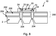
- Figure 8 shows a semiconductor device 10 according to another embodiment of this disclosure.
- the device is similar in some respects to that described above in relation to Figure 4 , and includes a mm wave interface 70 extending laterally within the encapsulant 20 as explained previously.
- the encapsulant 20 is mounted on an intermediate portion comprising a lead frame 200 (no separate substrate is provided).
- the lead frame 200 itself may be substantially as described above in relation to Figures 6 and 7 , and may include the aforementioned dielectric layer 206 having metalized surface layers 202, 204 provided thereon.
- the electrical interconnections between the components in the encapsulant 20 and the lead frame 200 may be implemented in a number of ways in this embodiment. For instance, it is envisaged that wire bonds may be provided between pads on a topside of a redistribution layer in the encapsulant 20 and the lead frame 200.
- the semiconductor device 10 in this embodiment includes a antenna portion 2 comprising a three dimensional (3D) antenna.
- the antenna portion 2 includes openings 204 for conveying electromagnetic radiation to the radiation transmitting and receiving parts in the encapsulant 20.
- the antenna portion 2 is electrically conductive (e.g. at least partially metallic).
- the antenna portion 2 is located on an opposite side of the lead frame 200 to the encapsulant 20.
- the lead frame 200 includes openings that are aligned with the openings 204 in the antenna portion 2 to allow electromagnetic radiation to be conveyed to the radiation transmitting and receiving parts 24 (e.g. the mm wave interface 70) in the encapsulant 20.
- lead frame 200 as an intermediate portion in the present embodiment again allows an electrically contiguous passage, without an air gap, to be formed for conveying the electromagnetic radiation from the antenna portion 2 to the radiation transmitting and receiving parts 24 in the encapsulant 20. In this way, the mismatch, insertion losses and radiation associated with the examples shown in Figure 1 and Figure 2 can be prevented.
- Figures 9A to 9D and Figure 10 each show an arrangement of openings in a semiconductor device 10 according to embodiments of this disclosure.
- the opening(s) of the antenna portion and the corresponding opening(s) of the intermediate portion may have substantially the same cross sectional shape and size when viewed along a direction parallel to a surface normal of a major surface of the intermediate portion. Matching the shapes of the various openings can prevent the presence of discontinuities in the path taken by the electromagnetic radiation, thereby to reduce losses.
- the cross sectional shape may, for instance, be circular ( Figure 9A ), square ( Figure 9B ), oblong ( Figures 9C , and 10 ), or elliptical ( Figure 9D ). Similar considerations apply to each of the embodiments described herein.
- the openings 204 may in some embodiments be integrated into a ground plane of the lead frame 200 as shown in each of Figures 9A to 9D , or may in other embodiments be integrated as a pad as shown in Figure 10 .
- FIG 11 shows an arrangement of rings 44 around the openings 204 in a semiconductor device 10 according to a further embodiment of this disclosure.
- Each ring 44 may be located in the dielectric 206 of the lead frame 200 and may extends between the metalized surface layers 202, 204.
- Each ring may, for instance, comprise a plurality of vias 42 filled with electrically conductive material.
- the vias may, for example, be plate through holes (PTHs) or may comprise metallic (e.g. Cu) via bars.
- PTHs plate through holes
- Cu metallic
- these rings 44 can serve as a further barrier to prevent radiation leakage from the openings 204, thereby preventing the electromagnetic radiation in one opening 204 from reaching another opening 204 in the device (e.g. through the dielectric 206).
- the device includes an encapsulant.
- the device also includes a semiconductor die in the encapsulant.
- the device further includes electromagnetic radiation transmitting and receiving parts in the encapsulant.
- the device also includes an intermediate portion having a first surface and a second surface. The first surface is attached to the encapsulant.
- the device also includes an antenna portion attached to the second surface of the intermediate portion.
- the antenna portion includes one or more openings for conveying electromagnetic radiation.
- the intermediate portion includes one or more corresponding openings aligned with the openings of the antenna portion. Each opening of the antenna portion and each corresponding opening of the intermediate portion forms an electrically contiguous passage for conveying the electromagnetic radiation to the electromagnetic radiation transmitting and receiving parts in the encapsulant.
Abstract
Description
- The present specification relates to a semiconductor device and method.
- Nowadays the trend goes to higher integration of mm wave transceivers in small packaged integrated circuits (ICs). Typical applications for such devices include automotive RADAR and 5G communication systems. As an example, RADAR ICs with integrated transmitters and receiver are available for automotive radar applications at 77GHz. Furthermore, large array antennas are used to realise multiple-input-multiple-output (MIMO) operation. This technique is widely used in modern radar and communication systems.
- Mm-wave packaged transceiver ICs are typically soldered on a printed circuit board (PCB). Examples of such devices are shown in
Figures 1 and 2 . - The
example device 11 inFigure 1 includes a semiconductor die 30 located in anencapsulant 20. Thedevice 11 also includes radiation transmitting and receivingparts 24. The radiation transmitting and receivingparts 24 may, for instance, comprise metallic portions located in theencapsulant 20 and electrically connected with the semiconductor die 30 (e.g. seeconnections 25 inFigure 1 ). - The
encapsulant 20 is mounted on asubstrate 40 such as a printed circuit board (PCB) usingsolder balls 42. Thesolder balls 42 provide for mechanical attachment of theencapsulant 20 to thesubstrate 40, and can also provide electrical connections between theencapsulant 20 containing thedie 30 and thesubstrate 40. - The
semiconductor device 11 also includes anantenna portion 2, which in the present example comprises a slot antenna array including a plurality ofslots 4. Theantenna portion 2 is at least partially metallic. Theantenna portion 2 is located on an opposite side of theencapsulant 20 to thesubstrate 40. - As shown in
Figure 1 , theslots 4 form openings which are aligned with the radiation transmitting and receivingparts 24, so that electromagnetic radiation passing along theslots 4 is incident upon the radiation transmitting and receivingparts 24. - The
example device 11 inFigure 2 also includes a semiconductor die 30 located in anencapsulant 20. Thedevice 11 also includes radiation transmitting and receivingparts 24. The radiation transmitting and receivingparts 24 may, for instance, comprise metallic portions located in theencapsulant 20 and electrically connected with the semiconductor die 30 (e.g. seeconnections 25 inFigure 2 ). - Again, the
encapsulant 20 is mounted on asubstrate 40 such as a printed circuit board (PCB) usingsolder balls 42. Thesolder balls 42 provide for mechanical attachment of theencapsulant 20 to thesubstrate 40, and can also provide electrical connections between the components located in theencapsulant 20 and thesubstrate 40. - The
semiconductor device 11 also includes aantenna portion 2, which in the present example again comprises a slot antenna array including a plurality ofslots 4. Again, theantenna portion 2 is at least partially metallic. - As shown in
Figure 1 , theslots 4 form openings which are aligned with the radiation transmitting and receivingparts 24. Note that in this example, theantenna portion 2 is mounted on an opposite side of thesubstrate 40 to the side of thesubstrate 40 upon which theencapsulant 20 is mounted. Thesubstrate 40 in this example includesopenings 44, which are lined withmetal 46. Theopenings 44 are aligned with theslots 4 and the radiation transmitting and receivingparts 24, so that electromagnetic radiation passing along theslots 4 is incident upon the radiation transmitting and receivingparts 24 via the openings. - It will be appreciated that the examples in
Figures 1 and 2 allow radiation to be transmitted and received from either "above" or "beneath" the encapsulant 20. - In both the examples in
Figures 1 and 2 , anair gap 50 is present between the radiation transmitting and receivingparts 24 of the device and the antenna portion 2 (Figure 1 ) or the substrate 40 (Figure 2 ). Thisair gap 50 can lead to discontinuities of the surface currents flowing between the radiation transmitting and receivingparts 24 and theantenna portion 2, causing mismatch, higher insertion losses and radiation, which decreases the isolation between the radiation transmitting and receivingparts 24 in thedevice 11. In communication and radar systems, high isolation (>30dB) between the mm-wave channel is generally required. - Aspects of the present disclosure are set out in the accompanying independent and dependent claims. Combinations of features from the dependent claims may be combined with features of the independent claims as appropriate and not merely as explicitly set out in the claims.
- According to an aspect of the present disclosure, there is provided a semiconductor device comprising:
- an encapsulant;
- a semiconductor die in the encapsulant;
electromagnetic radiation transmitting and receiving parts in the encapsulant; - an intermediate portion having a first surface and a second surface, wherein the first surface is attached to the encapsulant; and
- an antenna portion attached to the second surface of the intermediate portion,
- wherein the antenna portion includes one or more openings for conveying electromagnetic radiation,
- wherein the intermediate portion includes one or more corresponding openings aligned with the openings of the antenna portion, and
- wherein each opening of the antenna portion and each corresponding opening of the intermediate portion forms an electrically contiguous passage for conveying said electromagnetic radiation to the electromagnetic radiation transmitting and receiving parts in the encapsulant.
- According to another aspect of the present disclosure, there is provided a method of making a semiconductor device, the method comprising:
- encapsulating a semiconductor die and radiation transmitting and receiving parts in an encapsulant;
- providing an intermediate portion having a first surface and a second surface;
- attaching the first surface of the intermediate portion to the encapsulant;
- providing an antenna portion; and
- attaching the antenna portion to the second surface of the intermediate portion,
- wherein the antenna portion includes one or more openings for conveying electromagnetic radiation,
- wherein the intermediate portion includes one or more corresponding openings aligned with the openings of the antenna portion, and
- wherein each opening of the antenna portion and each corresponding opening of the intermediate portion forms an electrically contiguous passage for conveying said electromagnetic radiation to the electromagnetic radiation transmitting and receiving parts in the encapsulant.
- The provision of an electrically contiguous passage for conveying the electromagnetic radiation from the antenna portion to the electromagnetic radiation transmitting and receiving parts in the encapsulant can avoid the presence of mismatch, insertion losses and radiation associated with the presence of an air gap located between the encapsulant and the antenna portion in a semiconductor device.
- The intermediate portion may include a conductive elastomer. This can allow the antenna portion and the encapsulant to be attached together in such a way that the intermediate portion can absorb mechanical stress between the antenna portion and the encapsulant. The use of a conductive elastomer in this way can also improve the tolerances for the flatness of the surfaces of the antenna portion and the encapsulant that face each other. The conductive elastomer may also serve as a heat sink for moving heat from the encapsulant and the components located therein toward the antenna portion. Furthermore, the conductive elastomer can act as a shield to prevent EMC/EMI radiation.
- The intermediate portion may include a layer of the conductive elastomer. This can simplify the manufacturing process.
- The electromagnetic radiation transmitting and receiving parts may include one or more electrically conductive portions aligned with the opening(s) of the antenna portion and the corresponding opening(s) of the intermediate portion for transmitting and receiving the electromagnetic radiation.
- The encapsulant may include one or more openings lined with an electrically conductive material. The or each opening may be aligned with a respective one of the electrically contiguous passages, for conveying the electromagnetic radiation within the encapsulant. Again, this can allow the electromagnetic radiation to be conveyed without experiencing losses associated with gaps in the path that the radiation takes.
- Each of the electrically conductive portions for receiving the electromagnetic radiation may be at least partially located with a respective one of the openings in the encapsulant.
- The encapsulant may be further attached to a substrate.
- The intermediate portion may include a lead frame. This can enable a flip-chip arrangement in the encapsulant.
- The intermediate portion may further include a printed circuit board (PCB). The lead frame may be located in between the encapsulant and the printed circuit board. The printed circuit board may be located in between the lead frame and the antenna portion. The lead frame and the printed circuit board may each include one or more openings forming the corresponding openings of the intermediate portion aligned with the one or more openings of the antenna portion.
- The encapsulant may include one or more electrical connections for electrically connecting the semiconductor die to corresponding connections on the lead frame.
- The opening(s) of the antenna portion and the corresponding opening(s) of the intermediate portion may have substantially the same cross sectional shape and size when viewed along a direction parallel to a surface normal of the first surface of the intermediate portion. Matching the shapes of the various openings can prevent the presence of discontinuities in the path taken by the electromagnetic radiation, thereby to reduce losses. The cross sectional shape may, for instance, be square, oblong, circular or elliptical.
- The device may include at least one ring comprising electrically conductive material surrounding the electrically contiguous passage to prevent leakage of the electromagnetic radiation from the electrically contiguous passage. In some embodiments, the ring(s) may be located in a dielectric portion of a lead frame.
- Embodiments of this disclosure will be described hereinafter, by way of example only, with reference to the accompanying drawings in which like reference signs relate to like elements and in which:
-
Figure 1 shows an example of semiconductor device; -
Figure 2 shows another example of semiconductor device; -
Figure 3 shows a semiconductor device according to an embodiment of this disclosure; -
Figure 4 shows a semiconductor device according to an embodiment of this disclosure; -
Figure 5 shows an arrangement of openings in an elastomer layer according to an embodiment of this disclosure; -
Figure 6 shows a semiconductor device according to another embodiment of this disclosure; -
Figure 7 shows a semiconductor device according to a further embodiment of this disclosure; -
Figure 8 shows a semiconductor device according to another embodiment of this disclosure; -
Figures 9A to 9D each show an arrangement of openings in a semiconductor device according to further embodiments of this disclosure; -
Figure 10 shows an arrangement of openings in a semiconductor device according to another embodiment of this disclosure; and -
Figure 11 shows an arrangement solder balls around openings in a semiconductor device according to a further embodiment of this disclosure. - Embodiments of this disclosure are described in the following with reference to the accompanying drawings.
-
Figure 3 shows asemiconductor device 10 according to an embodiment of this disclosure. - The
device 10 inFigure 3 includes asemiconductor die 30 located in anencapsulant 20. Thedevice 10 also includes one or more radiation transmitting and receivingparts 24. The radiation transmitting and receivingparts 24 may, for instance, comprise metallic portions located in theencapsulant 20 and electrically connected with the semiconductor die 30 (these connections are not shown inFigure 3 ). - In this embodiment, the
encapsulant 20 is mounted on asubstrate 40 such as a printed circuit board (PCB) usingsolder balls 42. Thesolder balls 42 provide for mechanical attachment of theencapsulant 20 to thesubstrate 40, and can also provide electrical connections between the components located theencapsulant 20 and thesubstrate 40. Note that theencapsulant 20 may have pads on its underside (i.e. the side facing the substrate 40) to electrically connect with the solder balls. The semiconductor die 30 may be electrically connected to the pads using a redistribution layer, bond wires, or the like. - The
semiconductor device 10 also includes anantenna portion 2, which in the present example comprises a slot antenna array including a plurality ofslots 4. Theantenna portion 2 is electrically conductive (e.g. at least partially metallic). In this embodiment, theantenna portion 2 is located on an opposite side of theencapsulant 20 to thesubstrate 40. - As shown in
Figure 3 , theslots 4 form openings which are aligned with the radiation transmitting and receivingparts 24, so that electromagnetic radiation passing along theslots 4 is incident upon the radiation transmitting and receivingparts 24. - The
semiconductor device 10 also includes anintermediate portion 60. The intermediate portion is located in between the encapsulant 20 and theantenna portion 2. In particular, theintermediate portion 60 has a first surface which is attached to the encapsulant 20 (the "topside" of theencapsulant 20 in this embodiment) and a second surface (which is on an opposite side of the intermediate portion 60) which is attached to the ("underside" of the)antenna portion 2. - The
intermediate portion 60 includes one ormore openings 62. Theopenings 62 are aligned with the openings formed by theslots 4 of theantenna portion 2. Note that in this embodiment, theopenings 62 are also aligned with the radiation transmitting and receivingparts 24 in theencapsulant 20, whereby the openings formed by theslots 4, theopenings 62 and the radiation transmitting and receivingparts 24 are all in alignment. This can allow electromagnetic radiation to be conveyed to/from the radiation transmitting and receivingparts 24 in theencapsulant 20 through theantenna portion 2 and theintermediate portion 60. - As can be seen in
Figure 3 , theintermediate portion 60 in this embodiment completely fills the space between the encapsulant 20 and theantenna portion 2. Because of this, there is no air gap located between the encapsulant 20 and theantenna portion 2. Each opening formed by aslot 4 of theantenna portion 2 and eachcorresponding opening 62 in the intermediate portion may thus form an electrically contiguous passage for conveying the electromagnetic radiation to the radiation transmitting and receivingparts 24 in theencapsulant 20. In this way, the mismatch, insertion losses and radiation associated with the examples shown inFigure 1 and Figure 2 can be prevented. - In the present embodiment, the
intermediate portion 60 is provided in the form of a layer. The layer may be thinner than the width of theencapsulant 20 and/or theantenna portion 2. Theintermediate portion 60 may also perform the function of providing a means of attaching theantenna portion 2 to theencapsulant 20. - It is envisaged that in some embodiments, the
intermediate portion 60 may be provided in the form of a ring around the openings (e.g. in the form of a gasket). This can allow less material to be used and can reduce mechanical stresses between theantenna portion 2 and theencapsulant 20. - The intermediate portion in this embodiment comprises an elastomer. The elastomer is conductive, to allow the electrically contiguous passage for the electromagnetic radiation noted above to the implemented. For instance, the conductive elastomer may comprise silicone, flurorosilicone, or polyurethane, filled with conductive particles the particles may comprise, for example, Ag, Cu, Al, Ni carbon fibre, etc.). The use of a conductive elastomer may also allow the
antenna portion 2 to be mounted on theencapsulant 20 in such a way that mechanical stresses between the encapsulant 20 and theantenna portion 2 may be absorbed by theintermediate portion 60. -
Figure 4 shows asemiconductor device 10 according to another embodiment of this disclosure. In some respects, thesemiconductor device 10 in this embodiment is similar to the embodiment shown inFigure 3 . - The
device 10 inFigure 4 includes asemiconductor die 30 located in anencapsulant 20. The device includes one or more radiation transmitting and receivingparts 24. The radiation transmitting and receivingparts 24 in this embodiment include openings in theencapsulant 20. The openings may be lined with an electrically conductive material (e.g. a metal or alloy). The radiation transmitting and receivingparts 24 in this embodiment also include an mm wave interface 70 (e.g. dipole or back short). Theinterface 70 may extend laterally within theencapsulant 20 as shown inFigure 4 . The antenna is electrically connected to the semiconductor die 30. In this way, electromagnetic radiation can be conveyed through theantenna portion 102 and theintermediate portion 60 and provided to the antenna, for transmission and reception of the signal in the semiconductor die 30. - In this embodiment, the
encapsulant 20 is mounted on asubstrate 40 such as a printed circuit board (PCB) usingsolder balls 42. The substrate may, for instance, comprise FR4. Thesolder balls 42 provide for mechanical attachment of the encapsulant 20to thesubstrate 40, and can also provide electrical connections between the components inside theencapsulant 20 and thesubstrate 40. Again, theencapsulant 20 may include pads on its underside (i.e. the side facing the substrate 40) to electrically connect with the solder balls. The semiconductor die 30 may be electrically connected to the pads using a redistribution layer, bond wires, or the like. - The
semiconductor device 10 also includes aantenna portion 102, which in the present example comprises three dimensional (3D) antenna. Theantenna portion 102 includesopenings 104 for conveying electromagnetic radiation to the radiation transmitting and receivingparts 24 in theencapsulant 20. Theantenna portion 102 is electrically conductive (e.g. at least partially metallic). In this embodiment, the part of theantenna portion 102 including theopenings 104 is located on an opposite side of the radiation transmitting and receivingparts 24 to thesubstrate 40. Theantenna portion 102 may also include peripheral portions that are attached to thesubstrate 40 for additional mechanical stability. - As shown in
Figure 4 , theopenings 104 are aligned with the radiation transmitting and receivingparts 24, so that electromagnetic radiation passing along theopenings 104 is incident upon the radiation transmitting and receivingparts 24. - Again, the
semiconductor device 10 includes anintermediate portion 60, which is located in between the encapsulant 20 and the part of theantenna portion 102 including theopenings 104. In particular, theintermediate portion 60 has a first surface which is attached to the encapsulant 20 (the "topside" of theencapsulant 20 in this embodiment) and a second surface (which is on an opposite side of the intermediate portion 60) which is attached to the ("underside" of the) part of theantenna portion 102 including theopenings 104. - Again, the
intermediate portion 60 includes one ormore openings 62. Theopenings 62 are aligned with theopenings 104 of theantenna portion 102. Note that in this embodiment, theopenings 62 are again aligned with the radiation transmitting and receivingparts 24 in theencapsulant 20, whereby theopenings 104, theopenings 62 and the radiation transmitting and receivingparts 24 are all in alignment. This can allow electromagnetic radiation to be conveyed to/from the radiation transmitting and receivingparts 24 in theencapsulant 20 through theantenna portion 102 and theintermediate portion 60. - As can be seen in
Figure 4 , theintermediate portion 60 in this embodiment again completely fills the space between the encapsulant 20 and theantenna portion 102. Again, because of this, there is no air gap located between the encapsulant 20 and theantenna portion 102. Eachopening 104 and eachcorresponding opening 62 in the intermediate portion may thus form an electrically contiguous passage for conveying the electromagnetic radiation to the radiation transmitting and receivingparts 24 in theencapsulant 20. In this way, the mismatch, insertion losses and radiation associated with the examples shown inFigure 1 and Figure 2 can again be prevented. It is envisaged that the intermediate portion may be in the form of a rings around the openings (e.g. like a gasket) as noted above in relation to the embodiment ofFigure 3 . - In the present embodiment, the
intermediate portion 60 is again provided in the form of a layer. The layer may be thinner than the width of theencapsulant 20 and/or the antenna portion. Theintermediate portion 60 may also perform the function of providing a means of attaching theantenna portion 102 to theencapsulant 20, noting that the antenna portion may also be attached at its periphery to thesubstrate 40. - The intermediate portion in this embodiment again comprises an elastomer. The elastomer is conductive, to allow the electrically contiguous passage for the electromagnetic radiation noted above to the implemented. The use of an elastomer may also allow the
antenna portion 102 to be mounted on theencapsulant 20 in such a way that mechanical stresses between the encapsulant 20 and theantenna portion 102 may be absorbed by theintermediate portion 60. -
Figure 5 , which views thesemiconductor device 10 along a direction parallel to a surface normal of the abovementioned first surface of theintermediate portion 60, illustrates the alignment of theopenings 62 in theintermediate portion 60 with the radiation transmitting and receivingparts 24 in theencapsulant 20 in the embodiments ofFigures 3 and 4 . Note that the radiation transmitting and receivingparts 24 may be of similar or the same size and shape as theopenings 62 in theintermediate portion 60. The size and shape of the radiation transmitting and receivingparts 24 and theopenings 62 in theintermediate portion 60 may also be matched to the size and shape of theopenings 4/104 in theantenna portion 2/102. -
Figure 6 shows asemiconductor device 10 according to another embodiment of this disclosure. While in the embodiments ofFigures 3 to 5 , theantenna portion 2/102 is located on an opposite side (the "topside") of theencapsulant 20 to thesubstrate 40, in the embodiment ofFigure 6 , theantenna portion 2 is located on the same side of theencapsulant 20 as thesubstrate 40. Accordingly, embodiments of this disclosure can allow for mounting of theantenna portion 2/102 on either side (the "topside" or the "underside") of theencapsulant 20. - The
device 10 inFigure 6 includes asemiconductor die 30 located in anencapsulant 20. In this embodiment, thedevice 10 also includes a ballgrid array substrate 28 located in theencapsulant 20. The semiconductor die 30 is mounted on the ballgrid array substrate 28 in a flip chip fashion using solder or copper pillar bumps 32. - The
device 10 also includes one or more radiation receiving parts, which in this embodiment each include anopening 124 in theencapsulant 20. The opening(s) 124 may be lined with an electrically conductive material 126 (e.g. a metal or alloy). The opening(s) 124 may each terminate at the ballgrid array substrate 28, which may be provided with electrically conductive features (e.g. an antenna) for capturing the electromagnetic radiation and passing the associated signal via electrical connections to thesemiconductor substrate 30. - The
semiconductor device 10 in this embodiment includes asubstrate 40 such as a printed circuit board (PCB). Thesemiconductor device 10 in this embodiment further includes aantenna portion 2, which in the present example comprises a slot antenna array including a plurality of slots. Theantenna portion 2 is electrically conductive (e.g. at least partially metallic). As shown inFigure 6 , theslots 4 form openings which are aligned with theopenings 124 of the radiation transmitting and receiving parts, so that electromagnetic radiation passing along theslots 4 is incident upon the radiation transmitting and receiving parts. - In this embodiment, the
antenna portion 2 is located on an opposite side of thesubstrate 40 to theencapsulant 20. Thesubstrate 40 is provided with openings to allow electromagnetic radiation from theslots 4 in theantenna portion 2 to pass to theencapsulant 20. The openings in thesubstrate 40 may be lined with an electrically conductive material 246 (e.g. a metal or alloy). Theantenna portion 2 in this embodiment is mounted on a surface (the "underside") of thesubstrate 40. Note that the lining 246 of the openings in the substrate may extend laterally along the surface (the "underside") of thesubstrate 40, to prevent an air gap at the interface between theslots 4 and the openings in thesubstrate 40. - The
semiconductor device 10 also includes an intermediate portion. Note that in this embodiment, the intermediate portion includes two parts. The first part of the comprises alead frame 200. The second part of the intermediate portion comprises thesubstrate 40. Accordingly, in this embodiment, the intermediate portion is located in between the encapsulant 20 and theantenna portion 2. In particular, the intermediate portion has a surface (the "topside" of the lead frame 200) which is attached to the encapsulant 20 (the "underside" of the encapsulant 20) and a surface (the "underside" of the substrate 40) which is attached to the ("topside" of the)antenna portion 2. As can also be seen inFigure 6 , a surface (the "underside") of thelead frame 200 is attached to a surface (the "topside") of thesubstrate 40. - The
lead frame 200 may include adielectric layer 206 having metalized surface layers 202, 204 provided thereon. Thelayers substrate 40 and the components in theencapsulant 20. Note that thedevice 10 may includesolder balls 42 or other means for forming electrical connections between the ballgrid array substrate 28 and thelayer 202 of thelead frame 200. - The intermediate portion includes one or more openings. These openings are formed by the aforementioned openings in the substrate and corresponding openings that are provided in the
lead frame 200. The openings in thesubstrate 40 and corresponding openings in thelead frame 200 are aligned so as to allow electromagnetic radiation to pass through the intermediate portion. - The openings in the intermediate portion are aligned with the openings formed by the
slots 4 of theantenna portion 2. Accordingly, in this embodiment, the openings formed by theslots 4 in theantenna portion 2, the openings in the intermediate portion and the radiation transmitting and receivingparts 24 in theencapsulant 20 are all aligned to formpassages 208 to allow electromagnetic radiation to be conveyed to/from the radiation transmitting and receivingparts 24 in theencapsulant 20 through theantenna portion 2, the substrate and theintermediate portion 60 and thus transmitted and received by the radiation transmitting and receivingparts 124. - As can be seen in
Figure 6 , theintermediate portion 60 in this embodiment fills the space between the encapsulant 20 and theantenna portion 2. Because of this, there is no air gap located between the encapsulant 20 and theantenna portion 2. In particular, eachpassage 208 is an electrically contiguous passage for conveying the electromagnetic radiation to the radiation transmitting and receivingparts 124 in theencapsulant 20. In this way, the mismatch, insertion losses and radiation associated with the examples shown inFigure 1 and Figure 2 can be prevented. -
Figure 7 shows asemiconductor device 10 according to a further embodiment of this disclosure. Thesemiconductor device 10 inFigure 7 is similar to thesemiconductor device 10 ofFigure 6 , and only the significant differences will be described here. In particular, in the embodiment ofFigure 7 , thedevice 10 does not include a ball grid array substrate of the kind used in the embodiment ofFigure 6 . Instead, thedevice 10 includes a landgrid array substrate 34. The landgrid array substrate 34 may be incorporated in theencapsulant 20. This simplifies thedevice 10 and its electrical connections with the intermediate portion. The semiconductor die 30 is mounted on the ("topside" of the) landgrid array substrate 34 in a flip chip fashion using solder or copper pillar bumps 33. - A surface (the "underside") of the land
grid array substrate 34 may be attached using solder to the intermediate portion (namely, the "topside" of the lead frame 200). The surface (the "underside") of the landgrid array substrate 34 that is attached to thelead frame 200 may be provided with electrically conductive features (e.g. antennae) for transmitting and receiving electromagnetic radiation conveyed through thepassages 208. These features may form the radiation transmitting and receiving parts of the device in this embodiment. The transmitted and received signals may be passed from/to the semiconductor die 30 via electrical connections in the landgrid array substrate 34 and theland grid array 33. - As can be seen in
Figure 7 , theintermediate portion 60 in this embodiment again fills the space between the encapsulant 20 and theantenna portion 2. Because of this, there is no air gap located between the encapsulant 20 and theantenna portion 2. In particular, eachpassage 208 is an electrically contiguous passage for conveying the electromagnetic radiation to theencapsulant 20. In this way, the mismatch, insertion losses and radiation associated with the examples shown inFigure 1 and Figure 2 can be prevented. -
Figure 8 shows asemiconductor device 10 according to another embodiment of this disclosure. In this embodiment, the device is similar in some respects to that described above in relation toFigure 4 , and includes amm wave interface 70 extending laterally within theencapsulant 20 as explained previously. However, in the present embodiment, theencapsulant 20 is mounted on an intermediate portion comprising a lead frame 200 (no separate substrate is provided). - The
lead frame 200 itself may be substantially as described above in relation toFigures 6 and 7 , and may include theaforementioned dielectric layer 206 having metalized surface layers 202, 204 provided thereon. The electrical interconnections between the components in theencapsulant 20 and thelead frame 200 may be implemented in a number of ways in this embodiment. For instance, it is envisaged that wire bonds may be provided between pads on a topside of a redistribution layer in theencapsulant 20 and thelead frame 200. - The
semiconductor device 10 in this embodiment includes aantenna portion 2 comprising a three dimensional (3D) antenna. Theantenna portion 2 includesopenings 204 for conveying electromagnetic radiation to the radiation transmitting and receiving parts in theencapsulant 20. Theantenna portion 2 is electrically conductive (e.g. at least partially metallic). In this embodiment, theantenna portion 2 is located on an opposite side of thelead frame 200 to theencapsulant 20. As before, thelead frame 200 includes openings that are aligned with theopenings 204 in theantenna portion 2 to allow electromagnetic radiation to be conveyed to the radiation transmitting and receiving parts 24 (e.g. the mm wave interface 70) in theencapsulant 20. The use of thelead frame 200 as an intermediate portion in the present embodiment again allows an electrically contiguous passage, without an air gap, to be formed for conveying the electromagnetic radiation from theantenna portion 2 to the radiation transmitting and receivingparts 24 in theencapsulant 20. In this way, the mismatch, insertion losses and radiation associated with the examples shown inFigure 1 and Figure 2 can be prevented. -
Figures 9A to 9D andFigure 10 each show an arrangement of openings in asemiconductor device 10 according to embodiments of this disclosure. As can be seen from these figures, the opening(s) of the antenna portion and the corresponding opening(s) of the intermediate portion may have substantially the same cross sectional shape and size when viewed along a direction parallel to a surface normal of a major surface of the intermediate portion. Matching the shapes of the various openings can prevent the presence of discontinuities in the path taken by the electromagnetic radiation, thereby to reduce losses. The cross sectional shape may, for instance, be circular (Figure 9A ), square (Figure 9B ), oblong (Figures 9C , and10 ), or elliptical (Figure 9D ). Similar considerations apply to each of the embodiments described herein. Theopenings 204 may in some embodiments be integrated into a ground plane of thelead frame 200 as shown in each ofFigures 9A to 9D , or may in other embodiments be integrated as a pad as shown inFigure 10 . -
Figure 11 shows an arrangement ofrings 44 around theopenings 204 in asemiconductor device 10 according to a further embodiment of this disclosure. Eachring 44 may be located in the dielectric 206 of thelead frame 200 and may extends between the metalized surface layers 202, 204. Each ring may, for instance, comprise a plurality ofvias 42 filled with electrically conductive material. The vias may, for example, be plate through holes (PTHs) or may comprise metallic (e.g. Cu) via bars. An example arrangement ofvias 42 is shown in the detail on the right hand side ofFigure 11 . - The provision of these
rings 44 can serve as a further barrier to prevent radiation leakage from theopenings 204, thereby preventing the electromagnetic radiation in oneopening 204 from reaching anotheropening 204 in the device (e.g. through the dielectric 206). - Accordingly, there has been described a semiconductor device and a method of making the same. The device includes an encapsulant. The device also includes a semiconductor die in the encapsulant. The device further includes electromagnetic radiation transmitting and receiving parts in the encapsulant. The device also includes an intermediate portion having a first surface and a second surface. The first surface is attached to the encapsulant. The device also includes an antenna portion attached to the second surface of the intermediate portion. The antenna portion includes one or more openings for conveying electromagnetic radiation. The intermediate portion includes one or more corresponding openings aligned with the openings of the antenna portion. Each opening of the antenna portion and each corresponding opening of the intermediate portion forms an electrically contiguous passage for conveying the electromagnetic radiation to the electromagnetic radiation transmitting and receiving parts in the encapsulant.
- Although particular embodiments of this disclosure have been described, it will be appreciated that many modifications/additions and/or substitutions may be made within the scope of the claims.
Claims (15)
- A semiconductor device comprising:an encapsulant;a semiconductor die in the encapsulant;electromagnetic radiation transmitting and receiving parts in the encapsulant;an intermediate portion having a first surface and a second surface, wherein the first surface is attached to the encapsulant; andan antenna portion attached to the second surface of the intermediate portion,wherein the antenna portion includes one or more openings for conveying electromagnetic radiation,
wherein the intermediate portion includes one or more corresponding openings aligned with the openings of the antenna portion, and
wherein each opening of the antenna portion and each corresponding opening of the intermediate portion forms an electrically contiguous passage for conveying said electromagnetic radiation to the electromagnetic radiation transmitting and receiving parts in the encapsulant. - The device of claim 1, wherein the intermediate portion comprises a conductive elastomer.
- The device of claim 2, wherein the intermediate portion comprises a layer of said conductive elastomer.
- The device of any preceding claim, wherein the electromagnetic radiation transmitting and receiving parts comprise one or more electrically conductive portions aligned with the opening(s) of the antenna portion and the corresponding opening(s) of the intermediate portion for transmitting and receiving said electromagnetic radiation.
- The device of any preceding claim, wherein the encapsulant includes one or more openings lined with an electrically conductive material, wherein the or each opening is aligned with a respective one of said electrically contiguous passages, for conveying the electromagnetic radiation within the encapsulant.
- The device of claim 5 when dependent on claim 4, wherein each of said electrically conductive portions for receiving said electromagnetic radiation is at least partially located with a respective one of said openings in said encapsulant.
- The device of any preceding claim, wherein the encapsulant is further attached to a substrate.
- The device of claim 1, wherein the intermediate portion comprises a lead frame.
- The device of claim 8, wherein:the intermediate portion further comprises a printed circuit board (PCB),the lead frame is located in between the encapsulant and the printed circuit board,the printed circuit board is located in between the lead frame and the antenna portion, andthe lead frame and the printed circuit board each include one or more openings forming the corresponding openings of the intermediate portion aligned with the one or more openings of the antenna portion.
- The device of claim 8 or claim 9, wherein the device includes one or more electrical connections in the encapsulant for electrically connecting the semiconductor die to corresponding connections on the lead frame.
- The device of any preceding claim, comprising at least one ring comprising electrically conductive material surrounding said electrically contiguous passage to prevent leakage of said electromagnetic radiation from the electrically contiguous passage.
- The device of any preceding claim, wherein the opening(s) of the antenna portion and the corresponding opening(s) of the intermediate portion have substantially the same cross sectional shape and size when viewed along a direction parallel to a surface normal of said first surface of said intermediate portion.
- The device of claim 12, wherein said cross sectional shape is square, oblong, circular or elliptical.
- A method of making a semiconductor device, the method comprising:encapsulating a semiconductor die and radiation transmitting and receiving parts in an encapsulant;providing an intermediate portion having a first surface and a second surface;attaching the first surface of the intermediate portion to the encapsulant;providing an antenna portion; andattaching the antenna portion to the second surface of the intermediate portion,wherein the antenna portion includes one or more openings for conveying electromagnetic radiation,
wherein the intermediate portion includes one or more corresponding openings aligned with the openings of the antenna portion, and
wherein each opening of the antenna portion and each corresponding opening of the intermediate portion forms an electrically contiguous passage for conveying said electromagnetic radiation to the electromagnetic radiation transmitting and receiving parts in the encapsulant. - The method of claim 14, wherein the intermediate portion comprises a conductive elastomer.
Priority Applications (3)
| Application Number | Priority Date | Filing Date | Title |
|---|---|---|---|
| EP19188375.0A EP3771028A1 (en) | 2019-07-25 | 2019-07-25 | Semiconductor device and method |
| CN202010683626.2A CN112289779A (en) | 2019-07-25 | 2020-07-15 | Semiconductor device and method |
| US16/935,629 US11749624B2 (en) | 2019-07-25 | 2020-07-22 | Semiconductor device and method |
Applications Claiming Priority (1)
| Application Number | Priority Date | Filing Date | Title |
|---|---|---|---|
| EP19188375.0A EP3771028A1 (en) | 2019-07-25 | 2019-07-25 | Semiconductor device and method |
Publications (1)
| Publication Number | Publication Date |
|---|---|
| EP3771028A1 true EP3771028A1 (en) | 2021-01-27 |
Family
ID=67438913
Family Applications (1)
| Application Number | Title | Priority Date | Filing Date |
|---|---|---|---|
| EP19188375.0A Pending EP3771028A1 (en) | 2019-07-25 | 2019-07-25 | Semiconductor device and method |
Country Status (3)
| Country | Link |
|---|---|
| US (1) | US11749624B2 (en) |
| EP (1) | EP3771028A1 (en) |
| CN (1) | CN112289779A (en) |
Families Citing this family (1)
| Publication number | Priority date | Publication date | Assignee | Title |
|---|---|---|---|---|
| US20230127033A1 (en) * | 2021-10-25 | 2023-04-27 | Nxp Usa, Inc. | Semiconductor device with low loss waveguide interface and method therefor |
Citations (4)
| Publication number | Priority date | Publication date | Assignee | Title |
|---|---|---|---|---|
| US20020074654A1 (en) * | 2000-11-28 | 2002-06-20 | Kyocera Corporation | Wiring substrate, wiring board, and wiring substrate mounting structure |
| US6707138B2 (en) * | 1999-12-01 | 2004-03-16 | Amkor Technology, Inc. | Semiconductor device including metal strap electrically coupled between semiconductor die and metal leadframe |
| US20090066590A1 (en) * | 2007-09-07 | 2009-03-12 | Atsushi Yamada | Wireless communication device |
| US20120068316A1 (en) * | 2009-05-08 | 2012-03-22 | Telefonaktiebolaget L M Ericsson (Publ) | Transition from a chip to a waveguide port |
Family Cites Families (6)
| Publication number | Priority date | Publication date | Assignee | Title |
|---|---|---|---|---|
| KR100498708B1 (en) | 2004-11-08 | 2005-07-01 | 옵토팩 주식회사 | Electronic package for semiconductor device and packaging method thereof |
| US9219041B2 (en) | 2012-03-29 | 2015-12-22 | International Business Machines Corporation | Electronic package for millimeter wave semiconductor dies |
| US8998454B2 (en) * | 2013-03-15 | 2015-04-07 | Sumitomo Electric Printed Circuits, Inc. | Flexible electronic assembly and method of manufacturing the same |
| US9000599B2 (en) * | 2013-05-13 | 2015-04-07 | Intel Corporation | Multichip integration with through silicon via (TSV) die embedded in package |
| US9583811B2 (en) | 2014-08-07 | 2017-02-28 | Infineon Technologies Ag | Transition between a plastic waveguide and a semiconductor chip, where the semiconductor chip is embedded and encapsulated within a mold compound |
| WO2017160284A1 (en) * | 2016-03-16 | 2017-09-21 | Intel Corporation | Stairstep interposers with integrated shielding for electronics packages |
-
2019
- 2019-07-25 EP EP19188375.0A patent/EP3771028A1/en active Pending
-
2020
- 2020-07-15 CN CN202010683626.2A patent/CN112289779A/en active Pending
- 2020-07-22 US US16/935,629 patent/US11749624B2/en active Active
Patent Citations (4)
| Publication number | Priority date | Publication date | Assignee | Title |
|---|---|---|---|---|
| US6707138B2 (en) * | 1999-12-01 | 2004-03-16 | Amkor Technology, Inc. | Semiconductor device including metal strap electrically coupled between semiconductor die and metal leadframe |
| US20020074654A1 (en) * | 2000-11-28 | 2002-06-20 | Kyocera Corporation | Wiring substrate, wiring board, and wiring substrate mounting structure |
| US20090066590A1 (en) * | 2007-09-07 | 2009-03-12 | Atsushi Yamada | Wireless communication device |
| US20120068316A1 (en) * | 2009-05-08 | 2012-03-22 | Telefonaktiebolaget L M Ericsson (Publ) | Transition from a chip to a waveguide port |
Also Published As
| Publication number | Publication date |
|---|---|
| US11749624B2 (en) | 2023-09-05 |
| US20210028131A1 (en) | 2021-01-28 |
| CN112289779A (en) | 2021-01-29 |
Similar Documents
| Publication | Publication Date | Title |
|---|---|---|
| CN108231750B (en) | Radio frequency device package and forming method thereof | |
| KR101397748B1 (en) | Radio frequency(rf) integated circuit(ic) packages with integrated aperture-coupled patch antenna(s) | |
| TWI631834B (en) | Integrated circuit with electromagnetic communication | |
| US20210335724A1 (en) | Semiconductor Device with Partial EMI Shielding and Method of Making the Same | |
| US9941226B2 (en) | Integrated millimeter-wave chip package | |
| US7514774B2 (en) | Stacked multi-chip package with EMI shielding | |
| US8729680B2 (en) | Semiconductor device | |
| US8039930B2 (en) | Package structure for wireless communication module | |
| CN106935572B (en) | Method for improving BGA package isolation in radio frequency and millimeter wave products | |
| US7842546B2 (en) | Integrated circuit module and method of packaging same | |
| TWI557854B (en) | Integrated millimeter-wave chip package | |
| TW202203500A (en) | Low-cost, ipd and laminate based antenna array module | |
| US11749624B2 (en) | Semiconductor device and method | |
| KR20230064550A (en) | antenna-In-Package devices and methods of making | |
| KR102362243B1 (en) | Radio frequency package module and electronic apparatus including the same | |
| US11830798B2 (en) | Semiconductor device package | |
| KR20210018052A (en) | Antenna module and electronic device including thereof | |
| JP2012182682A (en) | High frequency device and high frequency module | |
| EP4336550A1 (en) | Semiconductor device with through package via and method therefor | |
| US20230317644A1 (en) | Routable multilevel package with multiple integrated antennas | |
| US20240071991A1 (en) | Method for making electronic package | |
| JP2007235149A (en) | Semiconductor device and electronic device | |
| CN117711956A (en) | Antenna structure in integrated package | |
| CN117594456A (en) | Semiconductor device and method for partial EMI shielding | |
| CN117219620A (en) | Semiconductor device and method using selective shielding of FOD material |
Legal Events
| Date | Code | Title | Description |
|---|---|---|---|
| PUAI | Public reference made under article 153(3) epc to a published international application that has entered the european phase |
Free format text: ORIGINAL CODE: 0009012 |
|
| STAA | Information on the status of an ep patent application or granted ep patent |
Free format text: STATUS: THE APPLICATION HAS BEEN PUBLISHED |
|
| AK | Designated contracting states |
Kind code of ref document: A1 Designated state(s): AL AT BE BG CH CY CZ DE DK EE ES FI FR GB GR HR HU IE IS IT LI LT LU LV MC MK MT NL NO PL PT RO RS SE SI SK SM TR |
|
| AX | Request for extension of the european patent |
Extension state: BA ME |
|
| STAA | Information on the status of an ep patent application or granted ep patent |
Free format text: STATUS: REQUEST FOR EXAMINATION WAS MADE |
|
| 17P | Request for examination filed |
Effective date: 20210727 |
|
| RBV | Designated contracting states (corrected) |
Designated state(s): AL AT BE BG CH CY CZ DE DK EE ES FI FR GB GR HR HU IE IS IT LI LT LU LV MC MK MT NL NO PL PT RO RS SE SI SK SM TR |
|
| STAA | Information on the status of an ep patent application or granted ep patent |
Free format text: STATUS: EXAMINATION IS IN PROGRESS |
|
| 17Q | First examination report despatched |
Effective date: 20230125 |