EP3769409B1 - Ansteuern eines metall-oxid-halbleiter-feldeffekttransistors - Google Patents
Ansteuern eines metall-oxid-halbleiter-feldeffekttransistors Download PDFInfo
- Publication number
- EP3769409B1 EP3769409B1 EP19727861.7A EP19727861A EP3769409B1 EP 3769409 B1 EP3769409 B1 EP 3769409B1 EP 19727861 A EP19727861 A EP 19727861A EP 3769409 B1 EP3769409 B1 EP 3769409B1
- Authority
- EP
- European Patent Office
- Prior art keywords
- drain
- mosfet
- body diode
- source
- voltage
- Prior art date
- Legal status (The legal status is an assumption and is not a legal conclusion. Google has not performed a legal analysis and makes no representation as to the accuracy of the status listed.)
- Active
Links
Images

Classifications
-
- H—ELECTRICITY
- H02—GENERATION; CONVERSION OR DISTRIBUTION OF ELECTRIC POWER
- H02M—APPARATUS FOR CONVERSION BETWEEN AC AND AC, BETWEEN AC AND DC, OR BETWEEN DC AND DC, AND FOR USE WITH MAINS OR SIMILAR POWER SUPPLY SYSTEMS; CONVERSION OF DC OR AC INPUT POWER INTO SURGE OUTPUT POWER; CONTROL OR REGULATION THEREOF
- H02M1/00—Details of apparatus for conversion
- H02M1/08—Circuits specially adapted for the generation of control voltages for semiconductor devices incorporated in static converters
- H02M1/083—Circuits specially adapted for the generation of control voltages for semiconductor devices incorporated in static converters for the ignition at the zero crossing of the voltage or the current
-
- H—ELECTRICITY
- H02—GENERATION; CONVERSION OR DISTRIBUTION OF ELECTRIC POWER
- H02M—APPARATUS FOR CONVERSION BETWEEN AC AND AC, BETWEEN AC AND DC, OR BETWEEN DC AND DC, AND FOR USE WITH MAINS OR SIMILAR POWER SUPPLY SYSTEMS; CONVERSION OF DC OR AC INPUT POWER INTO SURGE OUTPUT POWER; CONTROL OR REGULATION THEREOF
- H02M1/00—Details of apparatus for conversion
- H02M1/08—Circuits specially adapted for the generation of control voltages for semiconductor devices incorporated in static converters
-
- H—ELECTRICITY
- H02—GENERATION; CONVERSION OR DISTRIBUTION OF ELECTRIC POWER
- H02M—APPARATUS FOR CONVERSION BETWEEN AC AND AC, BETWEEN AC AND DC, OR BETWEEN DC AND DC, AND FOR USE WITH MAINS OR SIMILAR POWER SUPPLY SYSTEMS; CONVERSION OF DC OR AC INPUT POWER INTO SURGE OUTPUT POWER; CONTROL OR REGULATION THEREOF
- H02M3/00—Conversion of DC power input into DC power output
- H02M3/02—Conversion of DC power input into DC power output without intermediate conversion into AC
- H02M3/04—Conversion of DC power input into DC power output without intermediate conversion into AC by static converters
- H02M3/10—Conversion of DC power input into DC power output without intermediate conversion into AC by static converters using discharge tubes with control electrode or semiconductor devices with control electrode
- H02M3/145—Conversion of DC power input into DC power output without intermediate conversion into AC by static converters using discharge tubes with control electrode or semiconductor devices with control electrode using devices of a triode or transistor type requiring continuous application of a control signal
- H02M3/155—Conversion of DC power input into DC power output without intermediate conversion into AC by static converters using discharge tubes with control electrode or semiconductor devices with control electrode using devices of a triode or transistor type requiring continuous application of a control signal using semiconductor devices only
- H02M3/156—Conversion of DC power input into DC power output without intermediate conversion into AC by static converters using discharge tubes with control electrode or semiconductor devices with control electrode using devices of a triode or transistor type requiring continuous application of a control signal using semiconductor devices only with automatic control of output voltage or current, e.g. switching regulators
- H02M3/158—Conversion of DC power input into DC power output without intermediate conversion into AC by static converters using discharge tubes with control electrode or semiconductor devices with control electrode using devices of a triode or transistor type requiring continuous application of a control signal using semiconductor devices only with automatic control of output voltage or current, e.g. switching regulators including plural semiconductor devices as final control devices for a single load
- H02M3/1588—Conversion of DC power input into DC power output without intermediate conversion into AC by static converters using discharge tubes with control electrode or semiconductor devices with control electrode using devices of a triode or transistor type requiring continuous application of a control signal using semiconductor devices only with automatic control of output voltage or current, e.g. switching regulators including plural semiconductor devices as final control devices for a single load comprising at least one synchronous rectifier element
-
- H—ELECTRICITY
- H03—ELECTRONIC CIRCUITRY
- H03K—PULSE TECHNIQUE
- H03K17/00—Electronic switching or gating, i.e. not by contact-making and –breaking
- H03K17/08—Modifications for protecting switching circuit against overcurrent or overvoltage
- H03K17/082—Modifications for protecting switching circuit against overcurrent or overvoltage by feedback from the output to the control circuit
- H03K17/0822—Modifications for protecting switching circuit against overcurrent or overvoltage by feedback from the output to the control circuit in field-effect transistor switches
-
- H—ELECTRICITY
- H03—ELECTRONIC CIRCUITRY
- H03K—PULSE TECHNIQUE
- H03K17/00—Electronic switching or gating, i.e. not by contact-making and –breaking
- H03K17/16—Modifications for eliminating interference voltages or currents
- H03K17/161—Modifications for eliminating interference voltages or currents in field-effect transistor switches
- H03K17/165—Modifications for eliminating interference voltages or currents in field-effect transistor switches by feedback from the output circuit to the control circuit
-
- H—ELECTRICITY
- H02—GENERATION; CONVERSION OR DISTRIBUTION OF ELECTRIC POWER
- H02M—APPARATUS FOR CONVERSION BETWEEN AC AND AC, BETWEEN AC AND DC, OR BETWEEN DC AND DC, AND FOR USE WITH MAINS OR SIMILAR POWER SUPPLY SYSTEMS; CONVERSION OF DC OR AC INPUT POWER INTO SURGE OUTPUT POWER; CONTROL OR REGULATION THEREOF
- H02M1/00—Details of apparatus for conversion
- H02M1/0048—Circuits or arrangements for reducing losses
- H02M1/0054—Transistor switching losses
- H02M1/0058—Transistor switching losses by employing soft switching techniques, i.e. commutation of transistors when applied voltage is zero or when current flow is zero
-
- Y—GENERAL TAGGING OF NEW TECHNOLOGICAL DEVELOPMENTS; GENERAL TAGGING OF CROSS-SECTIONAL TECHNOLOGIES SPANNING OVER SEVERAL SECTIONS OF THE IPC; TECHNICAL SUBJECTS COVERED BY FORMER USPC CROSS-REFERENCE ART COLLECTIONS [XRACs] AND DIGESTS
- Y02—TECHNOLOGIES OR APPLICATIONS FOR MITIGATION OR ADAPTATION AGAINST CLIMATE CHANGE
- Y02B—CLIMATE CHANGE MITIGATION TECHNOLOGIES RELATED TO BUILDINGS, e.g. HOUSING, HOUSE APPLIANCES OR RELATED END-USER APPLICATIONS
- Y02B70/00—Technologies for an efficient end-user side electric power management and consumption
- Y02B70/10—Technologies improving the efficiency by using switched-mode power supplies [SMPS], i.e. efficient power electronics conversion e.g. power factor correction or reduction of losses in power supplies or efficient standby modes
Definitions
- the invention relates to a method and a control arrangement for controlling a metal-oxide-semiconductor field-effect transistor (MOSFET), in particular a MOSFET based on a wide-bandgap semiconductor.
- MOSFET metal-oxide-semiconductor field-effect transistor
- a MOSFET is reverse conductive and has a p-n junction between bulk and drain which, when the bulk and source are electrically connected, acts as an intrinsic diode, known as the inverse diode or the body diode of the MOSFET. Reverse currents flow through the body diode when the MOSFET is turned off. Since the body diode has a high resistance, this results in high losses. Significant losses of this type can occur in particular in a power converter designed using MOSFET technology if, in the event of a fault, all of the converter's MOSFETs are turned off and reverse currents from a supply network connected to the converter or a load connected to the converter flow through the body diodes of the converter's MOSFETs.
- MOSFETs based on semiconductors with a wide band gap, for example silicon carbide or gallium nitride, which are subject to high current loads.
- the problem arises that reverse currents through the MOSFETs can lead to high losses if all MOSFETs are switched off due to a fault.
- DE 11 2016 002 958 T2 discloses a method for controlling an electric power steering apparatus comprising a plurality of inverter bridges each connected to a multiphase motor configured to provide power assist for steering a vehicle.
- the method includes, upon detection of a failure within one of the inverter bridges, controlling current flow within the faulty inverter bridge and using one or more of the other inverter bridges to provide power assist.
- the invention is based on the object of specifying a method and a control arrangement for controlling a MOSFET, which are improved with regard to the reduction of losses caused by reverse currents.
- the object is achieved according to the invention by a method having the features of claim 1 and a control arrangement having the features of claim 5.
- the method according to the invention relates to the control of a MOSFET, in particular a MOSFET based on a semiconductor with a wide band gap, with a drain connection, a source connection, a gate connection and a body diode, wherein the MOSFET is arranged in a power converter having several MOSFETs.
- the invention therefore provides for switching on a MOSFET after the occurrence of a fault that has led to all MOSFETs of the power converter being switched off, if its body diode is conductive and therefore current-carrying.
- By switching on the MOSFET reverse currents that would flow through the body diode alone when the MOSFET is switched off are at least partially guided through the MOSFET channel between the source connection and the drain connection, so that reverse currents flowing through the body diode and the losses caused by them are greatly reduced.
- the body diode is electrically blocking, the MOSFET is controlled as usual depending on a control signal, so that the control of the MOSFET is not changed in this case.
- the invention further provides that a first voltage threshold value is specified for a drain-source voltage between the drain terminal and the source terminal of the MOSFET, the drain-source voltage is detected and it is concluded that the body diode is electrically conductive when the drain-source voltage falls below the first voltage threshold value. Furthermore, a second voltage threshold value is specified for the drain-source voltage and it is concluded that the body diode is electrically blocking when the drain-source voltage falls below the second voltage threshold value. For example, both voltage thresholds are negative and the second voltage threshold is greater than the first voltage threshold.
- the aforementioned aspects of the invention use the drain-source voltage to detect whether the body diode of the MOSFET is electrically conductive or blocking.
- voltage threshold values are used, which, when exceeded or undershot, signal that the body diode is electrically conductive or blocking.
- One embodiment of the invention provides that a first current threshold value is specified for a drain-source current intensity of a drain-source current flowing in a forward direction of the body diode between the drain terminal and the source terminal of the MOSFET, the drain-source current intensity is detected and it is concluded that the body diode is electrically conductive when the drain-source current intensity exceeds the first current threshold value. Furthermore, a second current threshold value for the drain-source current intensity, which is smaller than the first current threshold value, can be specified and it can be concluded that the body diode is electrically blocking when the drain-source current intensity falls below the second current threshold value.
- the invention provides that the direction of a drain-source current flowing between the drain terminal and the source terminal of the MOSFET is detected and it is concluded that the body diode is electrically conductive when the drain-source current flows in a forward direction of the body diode. Furthermore, it can be concluded that the body diode is electrically blocking when the drain-source current flows opposite to the forward direction of the body diode.
- the invention uses the drain-source current to detect whether the body diode is electrically conductive or blocking is.
- current threshold values are used for the current strength of the drain-source current in the forward direction of the body diode; if the threshold is exceeded or not reached, this signals that the body diode is electrically conductive or blocking.
- the drain-source current strength is measured, for example, using a shunt resistor that is arranged in the current path of the drain-source current.
- the direction of the drain-source current is recorded to determine whether the body diode is electrically conductive or blocking.
- the direction of the drain-source current is determined, for example, by counting the voltage pulses triggered or by a flip-flop that changes its state with each voltage pulse triggered.
- a control arrangement according to the invention for carrying out the method according to the invention comprises a monitoring unit which is designed to determine whether the body diode is electrically conductive or blocking, and a control unit which is designed, after the occurrence of a fault which has led to all MOSFETs of the power converter being switched off, to switch on the MOSFET if the monitoring unit determines that the body diode is electrically conductive, and to control the MOSFET as a function of the control signal if the body diode is electrically blocking.
- the monitoring unit is designed to detect the drain-source voltage and to determine, based on the drain-source voltage, whether the body diode is electrically conductive or blocking.
- Embodiments of the control arrangement according to the invention provide that the monitoring unit is designed to detect the drain-source current intensity and to determine, based on the drain-source current intensity, whether the body diode is electrically conductive or blocking, and/or that the monitoring unit is designed to detect the direction of the drain-source current and to determine, based on the direction of the drain-source current, whether the body diode is electrically conductive or blocking.
- a further embodiment of the control arrangement according to the invention provides that the monitoring unit is designed to inform the control unit by means of an additional control signal whether the body diode is electrically conductive or blocking, and the control unit has an output stage for controlling the MOSFET depending on the additional control signal and the control signal.
- An alternative embodiment of the control arrangement according to the invention provides that the monitoring unit is designed to inform the control unit by means of an additional control signal whether the body diode is electrically conductive or blocking, and the control unit has a first output stage for controlling the MOSFET depending on the control signal in the event that the body diode is electrically blocking, and a second output stage for controlling the MOSFET depending on the additional control signal in the event that the body diode is electrically conductive.
- a control arrangement according to the invention enables the implementation of the method according to the invention.
- the advantages of a control arrangement according to the invention therefore correspond to the advantages of the method according to the invention already mentioned above and are not listed separately again here.
- the invention modifies the control of a MOSFET only after the occurrence of a fault that has led to all MOSFETs of the power converter being switched off in the event that the body diode is electrically conductive.
- a control arrangement is used that extends the usual control to include the additional function of switching the MOSFET on after the occurrence of the fault if the body diode is electrically conductive.
- the usual control of the MOSFET and the usual protection concept remain unaffected by the invention.
- a power converter according to the invention in particular a traction power converter, has several MOSFETs, in particular several each based on a semiconductor with a wide band gap MOSFET, and for each MOSFET a control arrangement according to the invention for controlling the MOSFET.
- the invention is particularly suitable for controlling a MOSFET of a traction converter, since current loads on a MOSFET of a traction converter, in particular due to reverse currents, can be very high and can therefore cause high losses.
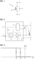
- FIG 1 shows a circuit diagram of a MOSFET 1 with a drain terminal D, a source terminal S, a gate terminal G and a body diode 2.
- the MOSFET 1 is designed as a normally blocking n-channel MOSFET based on a semiconductor with a wide band gap, for example silicon carbide or gallium nitride. Reverse currents, i.e. currents that are directed (according to the technical current direction) from the source terminal S to the drain terminal D, flow through the body diode 2 when the MOSFET 1 is switched off.
- FIG 2 shows a circuit diagram of a FIG 1 designed MOSFET 1 and a first embodiment of a control arrangement 3 according to the invention for controlling the MOSFET 1.
- the control arrangement 3 comprises a monitoring unit 5 and a control unit 7.
- the monitoring unit 5 is designed to determine whether the body diode 2 of the MOSFET 1 is electrically conductive or blocking and to communicate this to the control unit 7. To do this, the monitoring unit 5 detects a drain-source voltage U between the drain connection D and the source connection S of the MOSFET 1 and outputs a binary additional control signal S2 to the control unit 7 that is dependent on the drain-source voltage U and assumes the value 0 or the value 1.
- the value 1 of the additional control signal S2 signals that the body diode 2 is electrically conductive.
- the value 0 of the additional control signal S2 signals that the body diode 2 is electrically blocking.
- FIG 3 shows the additional control signal S2 output by the monitoring unit 5 as a function of the drain-source voltage U.
- the additional control signal S2 takes on the value 1 if the drain-source voltage U falls below a predetermined first voltage threshold U1.
- the additional control signal S2 takes on the value 0 if the drain-source voltage U exceeds a predetermined second voltage threshold U2.
- Both voltage thresholds U1, U2 are negative, with the second voltage threshold U2 being greater than the first voltage threshold U1.
- the first voltage threshold U1 has a value of approximately -1 V and the second voltage threshold U2 has a value of approximately -0.5 V.
- the additional control signal S2 is not changed, i.e. it retains its current value.
- the MOSFET 1 is arranged in a power converter 19, which has several MOSFETs 1 (see also FIG 4 ).
- the control unit 7 controls the MOSFET 1 depending on a binary control signal S1, which takes on the value 0 or the value 1, and after the occurrence of an error which has led to all MOSFETs 1 of the power converter 19 being switched off, additionally depending on the additional control signal S2.
- the control unit 7 has an OR gate 9 and an output stage 11.
- the control signal S1 and the additional control signal S2 are fed to the OR gate 9.
- the OR gate 9 outputs the value 0 to the output stage 11 if both the control signal S1 and the additional control signal S2 take on the value 0. Otherwise, the OR gate 9 outputs the value 1 to the output stage 11.
- the output stage 11 switches the MOSFET 1 on by placing a positive switch-on voltage between the gate connection G and the source connection S of the MOSFET 1. Otherwise, the output stage 11 switches off the MOSFET 1 by applying a switch-off voltage between the gate terminal G and the source terminal S of the MOSFET 1.
- FIG 4 shows a circuit diagram of a power converter 19 with a MOSFET 1 and a second embodiment of a control arrangement 3 according to the invention for controlling the MOSFET 1.
- the power converter 19 is, for example, a traction power converter with further MOSFETs 1 (not shown here), which are connected in a known manner to form half or full bridges, and a further control arrangement 3 for each further MOSFET 1.
- control arrangements 3 of this embodiment differ from that in FIG 2 shown embodiment merely by the design of the control units 7.
- a control unit 7 of this embodiment has two output stages 11, 13 and a switch 15.
- a control signal S1 is fed to a first output stage 11.
- the additional control signal S2 output by the monitoring unit 5 of the respective control arrangement 3 is fed to the second output stage 13.
- the switch 15 separates an output of the first output stage 11 from the gate terminal G of the MOSFET 1 controlled by the control arrangement 3 when the additional control signal S2 assumes the value 1.
- the MOSFET 1 is switched on by the second output stage 13 in that the second output stage 13 applies a positive switch-on voltage between the gate terminal G and the source terminal S of the MOSFET 1.
- the output of the first output stage 11 is connected by the switch 15 to the gate terminal G of the MOSFET 1 controlled by the control arrangement 3 and the MOSFET 1 is controlled by the first output stage 11, i.e. no voltage is applied by the second output stage 13 between the gate terminal G and the source terminal S of the MOSFET 1 and the MOSFET 1 is switched on by the first output stage 11 when the control signal S1 assumes the value 1 and switched off when the control signal S1 assumes the value 0.
- the control signals S1 for the MOSFET 1 of the power converter 19 are generated by a controller 17 of the power converter 19. It can be provided that the control of the MOSFET 1 is only activated by the second output stages 13 as a function of the additional control signals S2 if the controller 17 gives the release for this.
- FIG 5 shows a flow chart of an embodiment of the method according to the invention for controlling a MOSFET 1 with a FIG 2 or FIG 4 executed control arrangement 3.
- the voltage threshold values U1, U2 for the drain-source voltage U are specified.
- the drain-source voltage U is detected by the monitoring unit 5 and the additional control signal S2 is determined as a function of the drain-source voltage U in the manner described above with reference to FIG 3 described manner and output to the control unit 7.
- a third method step 23 the MOSFET 1 is switched on by the control unit 7 after the occurrence of a fault which has led to all MOSFETs 1 of the power converter 19 being switched off, i.e. a switch-on voltage is applied between the gate terminal G and the source terminal S of the MOSFET 1 if the additional control signal S2 assumes the value 1. Otherwise, the MOSFET 1 is controlled by the control unit 7 depending on the control signal S1, i.e. the switch-on voltage is applied between the gate terminal G and the source terminal S of the MOSFET 1 if the control signal S1 assumes the value 1, or a switch-off voltage is applied between the gate terminal G and the source terminal S of the MOSFET 1 if the control signal S1 assumes the value 0.
- the method continues with the second method step 22.
- control arrangement 3 according to the invention and of the method according to the invention described above with reference to the figures can be modified in various ways to form alternative exemplary embodiments.
- monitoring unit 5 can be designed in a different way than in the exemplary embodiments described above with reference to the figures.
- the monitoring unit 5 can be designed to detect and evaluate a drain-source current intensity of a drain-source current flowing in a forward direction of the body diode 2 between the drain terminal D and the source terminal S instead of the drain-source voltage U.
- a first current threshold value for the drain-source current intensity and a second current threshold value for the drain-source current intensity, which is smaller than the first current threshold value are specified.
- the additional control signal S2 is set to the value 1 if the drain-source current intensity exceeds the first current threshold value.
- the additional control signal S2 is set to the value 0 if the drain-source current intensity exceeds the first current threshold value. If the drain-source current is between the two current threshold values, the additional control signal S2 is not changed, i.e. it retains its current value.
- the drain-source current is measured, for example, with a shunt resistor that is arranged in the current path of the drain-source current.
- the monitoring unit 5 can be designed to detect a direction of the drain-source current.
- the additional control signal S2 is set to the value 1 if the drain-source current flows in the forward direction of the body diode 2. Otherwise, the additional control signal S2 is set to the value 0.
- the direction of the drain-source current is determined using a ferromagnetic core that triggers a voltage pulse every time the direction of the drain-source current changes. The direction of the drain-source current is determined, for example, by counting the voltage pulses triggered or by a flip-flop that changes its state every time a voltage pulse is triggered.
- FIG 4 Alternative embodiments of a power converter 19 result from replacing the FIG 4 shown control arrangement 3 by a control arrangement 3 of the embodiment described in Figure 2 or one of the aforementioned modified embodiments.
Landscapes
- Engineering & Computer Science (AREA)
- Power Engineering (AREA)
- Power Conversion In General (AREA)
- Electronic Switches (AREA)
- Insulated Gate Type Field-Effect Transistor (AREA)
- Emergency Protection Circuit Devices (AREA)
Description
- Die Erfindung betrifft ein Verfahren und eine Ansteueranordnung zum Ansteuern eines Metall-Oxid-Halbleiter-Feldeffekttransistors (MOSFET = Metal-Oxide-Semiconductor Field-Effect Transistor), insbesondere eines auf einem Halbleiter mit breitem Bandabstand (Wide-Bandgap Semiconductor) basierenden MOSFET.
- Ein MOSFET ist rückwärts leitfähig und weist einen p-n-Übergang zwischen Bulk und Drain auf, der bei elektrischer Verbindung von Bulk und Source als eine intrinsische Diode wirkt, die als Inversdiode oder als Bodydiode des MOSFET bezeichnet wird. Rückwärtsströme fließen durch die Bodydiode, wenn der MOSFET ausgeschaltet ist. Da die Bodydiode einen hohen Widerstand aufweist, entstehen dabei hohe Verluste. Beträchtliche Verluste dieser Art können insbesondere in einem in MOSFET-Technologie ausgeführten Stromrichter auftreten, wenn in einem Fehlerfall alle MOSFET des Stromrichters ausgeschaltet werden und Rückwärtsströme aus einem mit dem Stromrichter verbundenen Vorsorgungsnetz oder einer mit dem Stromrichter verbundenen Last durch Bodydioden der MOSFET des Stromrichters fließen. Gegenwärtig werden in bestimmten Stromrichtern, beispielsweise in Traktionsstromrichtern, vermehrt MOSFET eingesetzt, die auf Halbleitern mit breitem Bandabstand, beispielsweise auf Siliciumcarbid oder Galliumnitrid, basieren und hohen Strombelastungen ausgesetzt sind. Insbesondere in diesen Stromrichtern entsteht daher das Problem, dass Rückwärtsströme durch die MOSFET bei einem fehlerbedingten Ausschalten aller MOSFET zu hohen Verlusten führen können.
- Das Dokument Texas Instruments: "UCD7138 4-A and 6-A Single-Channel Synchronous-Rectifier Driver With Body-Diode Conduction Sensing and Reporting", 31. Mai 2015 (2015-05-31), URL: http://www.ti.com/lit/ds/symlink/ucd7138.pdf offenbart einen MOSFET-Treiber mit einem Gate-Treiber, einer Schaltung zum Erfassen eines Bodydiodenleitzustands und einer Schaltung zum Optimieren einer Einschaltverzögerung.
-
DE 11 2016 002 958 T2 offenbart ein Verfahren zum Steuern einer elektrischen Servolenkungsvorrichtung, die mehrere Wechselrichterbrücken umfasst, die jeweils mit einem Mehrphasenmotor verbunden sind, der zum Bereitstellen einer Leistungsunterstützung zur Lenkung eines Fahrzeugs konfiguriert ist. Das Verfahren umfasst nach einer Detektion eines Ausfalls innerhalb einer der Wechselrichterbrücken ein Steuern des Stromflusses innerhalb der fehlerhaften Wechselrichterbrücke und ein Verwenden einer oder mehrerer der anderen Wechselrichterbrücken, damit eine Leistungsunterstützung bereitgestellt wird. - Helen Ding: "IR11688 Smart Rectifier(TM) Control 1C Design Notes", 31. Juli 2015 (2015-07-31), Seiten 1-35, XP055715572, gefunden im Internet: URL:https://www.infineon.com/dgdl/lnfineon-ApplicationNote-1R11688-SmartRectifier-Control-1C-DesignNotes-AN-v01_00-EN.pdf fileld=5546d46253f65057015418afca1 d4d20 [gefunden am 2020-07-16] offenbart ein Verfahren zum Ansteuern eines MOSFET.
- Der Erfindung liegt die Aufgabe zugrunde, ein Verfahren und eine Ansteueranordnung zum Ansteuern eines MOSFET anzugeben, die hinsichtlich der Reduzierung von durch Rückwärtsströme verursachten Verlusten verbessert sind.
- Die Aufgabe wird erfindungsgemäß durch ein Verfahren mit den Merkmalen des Anspruchs 1 und eine Ansteueranordnung mit den Merkmalen des Anspruchs 5 gelöst.
- Vorteilhafte Ausgestaltungen der Erfindung sind Gegenstand der Unteransprüche.
- Das erfindungsgemäße Verfahren betrifft das Ansteuern eines MOSFET, insbesondere eines auf einem Halbleiter mit breitem Bandabstand basierenden MOSFET, mit einem Drain-Anschluss, einem Source-Anschluss, einem Gate-Anschluss und einer Body-diode, wobei der MOSFET in einem mehrere MOSFET aufweisenden Stromrichter angeordnet ist. Dabei wird nach dem Auftreten eines Fehlerfalls, der zu einem Ausschalten aller MOSFET des Stromrichters geführt hat, überwacht, ob die Bodydiode des MOSFET elektrisch leitend ist. Der MOSFET wird eingeschaltet, wenn die Bodydiode elektrisch leitend ist, und der MOSFET wird in Abhängigkeit von einem Ansteuersignal angesteuert, wenn die Bodydiode elektrisch sperrend ist.
- Die Erfindung sieht also vor, nach dem Auftreten eines Fehlerfalls, der zu einem Ausschalten aller MOSFET des Stromrichters geführt hat, einen MOSFET einzuschalten, wenn seine Bodydiode leitend und somit stromführend ist. Durch das Einschalten des MOSFET werden Rückwärtsströme, die im ausgeschalteten Zustand des MOSFET allein durch die Bodydiode fließen würden, zumindest teilweise durch den MOSFET-Kanal zwischen dem Source-Anschluss und dem Drain-Anschluss geführt, so dass durch die Bodydiode fließende Rückwärtsströme und die dadurch verursachten Verluste stark reduziert werden. Wenn die Bodydiode elektrisch sperrend ist, wird der MOSFET wie üblich in Abhängigkeit von einem Ansteuersignal angesteuert, so dass die Ansteuerung des MOSFET in diesem Fall nicht geändert wird.
- Die Erfindung sieht ferner vor, dass ein erster Spannungs-Schwellenwert für eine Drain-Source-Spannung zwischen dem Drain-Anschluss und dem Source-Anschluss des MOSFET vorgegeben wird, die Drain-Source-Spannung erfasst wird und darauf geschlossen wird, dass die Bodydiode elektrisch leitend ist, wenn die Drain-Source-Spannung den ersten Spannungs-Schwellenwert unterschreitet. Ferner wird ein zweiter Spannungs-Schwellenwert für die Drain-Source-Spannung vorgegeben und darauf geschlossen, dass die Bodydiode elektrisch sperrend ist, wenn die Drain-Source-Spannung den zweiten Spannungs-Schwellenwert überschreitet. Beispielsweise sind beide Spannungs-Schwellenwerte negativ und der zweite Spannungs-Schwellenwert ist größer als der erste Spannungs-Schwellenwert.
- Die vorgenannten Aspekte der Erfindung nutzen die Drain-Source-Spannung, um zu erkennen, ob die Bodydiode des MOSFET elektrisch leitend oder sperrend ist. Dazu werden Spannungs-Schwellenwerte verwendet, deren Unter- beziehungsweise Überschreiten signalisieren, dass die Bodydiode elektrisch leitend beziehungsweise sperrend ist.
- Eine Ausgestaltung der Erfindung sieht vor, dass ein erster Strom-Schwellenwert für eine Drain-Source-Stromstärke eines in einer Durchlassrichtung der Bodydiode zwischen dem Drain-Anschluss und dem Source-Anschluss des MOSFET fließenden Drain-Source-Stroms vorgegeben wird, die Drain-Source-Stromstärke erfasst wird und darauf geschlossen wird, dass die Bodydiode elektrisch leitend ist, wenn die Drain-Source-Stromstärke den ersten Strom-Schwellenwert überschreitet. Ferner kann ein zweiter Strom-Schwellenwert für die Drain-Source-Stromstärke, der kleiner als der erste Strom-Schwellenwert ist, vorgegeben werden und darauf geschlossen werden, dass die Bodydiode elektrisch sperrend ist, wenn die Drain-Source-Stromstärke den zweiten Strom-Schwellenwert unterschreitet.
- Die Erfindung sieht vor, dass die Richtung eines zwischen dem Drain-Anschluss und dem Source-Anschluss des MOSFET fließenden Drain-Source-Stroms erfasst wird und darauf geschlossen wird, dass die Bodydiode elektrisch leitend ist, wenn der Drain-Source-Strom in einer Durchlassrichtung der Bodydiode fließt. Ferner kann darauf geschlossen werden, dass die Body-diode elektrisch sperrend ist, wenn der Drain-Source-Strom entgegengesetzt zu der Durchlassrichtung der Bodydiode fließt.
- Die Erfindung nutzt dabei den Drain-Source-Strom, um zu erkennen, ob die Bodydiode elektrisch leitend oder sperrend ist. Dazu werden Strom-Schwellenwerte für die Stromstärke des Drain-Source-Stroms in der Durchlassrichtung der Bodydiode verwendet, deren Unter- beziehungsweise Überschreiten signalisieren, dass die Bodydiode elektrisch leitend beziehungsweise sperrend ist. Die Drain-Source-Stromstärke wird beispielsweise mit einem Shuntwiderstand gemessen, der in dem Strompfad des Drain-Source-Stroms angeordnet ist. Alternativ oder zusätzlich wird die Richtung des Drain-Source-Stroms erfasst, um zu erkennen, ob die Bodydiode elektrisch leitend oder sperrend ist. Die Richtung des Drain-Source-Stroms wird beispielsweise durch eine Zählung der ausgelösten Spannungsimpulse oder durch ein Flipflop, das bei jedem ausgelösten Spannungsimpuls seinen Zustand ändert, bestimmt.
- Eine erfindungsgemäße Ansteueranordnung zur Durchführung des erfindungsgemäßen Verfahrens umfasst eine Überwachungseinheit, die dazu ausgebildet ist, zu ermitteln, ob die Bodydiode elektrisch leitend oder sperrend ist, und eine Steuereinheit, die dazu ausgebildet ist, nach dem Auftreten eines Fehlerfalls, der zu einem Ausschalten aller MOSFET des Stromrichters geführt hat, den MOSFET einzuschalten, wenn die Überwachungseinheit ermittelt, dass die Bodydiode elektrisch leitend ist, und den MOSFET in Abhängigkeit von dem Ansteuersignal anzusteuern, wenn die Bodydiode elektrisch sperrend ist.
- Die Überwachungseinheit ist dazu ausgebildet, die Drain-Source-Spannung zu erfassen und anhand der Drain-Source-Spannung zu ermitteln, ob die Bodydiode elektrisch leitend oder sperrend ist. Ausgestaltungen der erfindungsgemäßen Ansteueranordnung sehen vor, dass die Überwachungseinheit dazu ausgebildet ist, die Drain-Source-Stromstärke zu erfassen und anhand der Drain-Source-Stromstärke zu ermitteln, ob die Bodydiode elektrisch leitend oder sperrend ist, oder/und dass die Überwachungseinheit dazu ausgebildet ist, die Richtung des Drain-Source-Stroms zu erfassen und anhand der Richtung des Drain-Source-Stroms zu ermitteln, ob die Bodydiode elektrisch leitend oder sperrend ist.
- Eine weitere Ausgestaltung der erfindungsgemäßen Ansteueranordnung sieht vor, dass die Überwachungseinheit dazu ausgebildet ist, der Steuereinheit durch ein Zusatzansteuersignal mitzuteilen, ob die Bodydiode elektrisch leitend oder sperrend ist, und die Steuereinheit eine Endstufe zur Ansteuerung des MOSFET in Abhängigkeit von dem Zusatzansteuersignal und dem Ansteuersignal aufweist. Eine dazu alternative Ausgestaltung der erfindungsgemäßen Ansteueranordnung sieht vor, dass die Überwachungseinheit dazu ausgebildet ist, der Steuereinheit durch ein Zusatzansteuersignal mitzuteilen, ob die Body-diode elektrisch leitend oder sperrend ist, und die Steuereinheit eine erste Endstufe zur Ansteuerung des MOSFET in Abhängigkeit von dem Ansteuersignal im Fall, dass die Bodydiode elektrisch sperrend ist, und eine zweite Endstufe zur Ansteuerung des MOSFET in Abhängigkeit von dem Zusatzansteuersignal im Fall, dass die Bodydiode elektrisch leitend ist, aufweist.
- Eine erfindungsgemäße Ansteueranordnung ermöglicht die Durchführung des erfindungsgemäßen Verfahrens. Die Vorteile einer erfindungsgemäßen Ansteueranordnung entsprechen daher den oben bereits genannten Vorteilen des erfindungsgemäßen Verfahrens und werden hier nicht noch einmal gesondert aufgeführt.
- Insgesamt modifiziert die Erfindung die Ansteuerung eines MOSFET nur nach dem Auftreten eines Fehlerfalls, der zu einem Ausschalten aller MOSFET des Stromrichters geführt hat, in dem Fall, dass die Bodydiode elektrisch leitend ist. Dazu wird eine Ansteueranordnung verwendet, die die übliche Ansteuerung um die Zusatzfunktion erweitert, den MOSFET nach dem Auftreten des Fehlerfalls einzuschalten, wenn die Bodydiode elektrisch leitend ist. Abgesehen davon bleiben die übliche Ansteuerung des MOSFET und das übliche Schutzkonzept von der Erfindung unberührt.
- Ein erfindungsgemäßer Stromrichter, insbesondere ein Traktionsstromrichter, weist mehrere MOSFET, insbesondere mehrere jeweils auf einem Halbleiter mit breitem Bandabstand basierende MOSFET, und für jeden MOSFET eine erfindungsgemäße Ansteueranordnung zum Ansteuern des MOSFET auf. Die Erfindung eignet sich insbesondere für das Ansteuern eines MOSFET eines Traktionsstromrichters, da Strombelastungen eines MOSFET eines Traktionsstromrichters, insbesondere durch Rückwärtsströme, sehr hoch sein können und daher hohe Verluste verursachen können.
- Die oben beschriebenen Eigenschaften, Merkmale und Vorteile dieser Erfindung sowie die Art und Weise, wie diese erreicht werden, werden klarer und deutlicher verständlich im Zusammenhang mit der folgenden Beschreibung von Ausführungsbeispielen, die im Zusammenhang mit den Zeichnungen näher erläutert werden. Dabei zeigen:
- FIG 1
- einen Schaltplan eines MOSFET,
- FIG 2
- einen Schaltplan eines MOSFET und eines ersten Ausführungsbeispiels einer Ansteueranordnung zum Ansteuern des MOSFET,
- FIG 3
- ein Zusatzansteuersignal in Abhängigkeit von einer Drain-Source-Spannung eines MOSFET,
- FIG 4
- einen Schaltplan eines Stromrichters,
- FIG 5
- ein Ablaufdiagramm eines Verfahrens zum Ansteuern eines MOSFET.
- Einander entsprechende Teile sind in den Figuren mit denselben Bezugszeichen versehen.
-
FIG 1 zeigt einen Schaltplan eines MOSFET 1 mit einem Drain-Anschluss D, einem Source-Anschluss S, einem Gate-Anschluss G und einer Bodydiode 2. Der MOSFET 1 ist als ein normal sperrender n-Kanal-MOSFET ausgebildet, der auf einem Halbleiter mit breitem Bandabstand, beispielsweise auf Siliciumcarbid oder Galliumnitrid, basiert. Rückwärtsströme, das heißt Ströme, die (gemäß technischer Stromrichtung) von dem Source-Anschluss S zu dem Drain-Anschluss D gerichtet sind, fließen im ausgeschalteten Zustand des MOSFET 1 durch die Bodydiode 2. -
FIG 2 zeigt einen Schaltplan eines wie inFIG 1 ausgebildeten MOSFET 1 und eines ersten Ausführungsbeispiels einer erfindungsgemäßen Ansteueranordnung 3 zum Ansteuern des MOSFET 1. - Die Ansteueranordnung 3 umfasst eine Überwachungseinheit 5 und eine Steuereinheit 7. Die Überwachungseinheit 5 ist dazu ausgebildet, zu ermitteln, ob die Bodydiode 2 des MOSFET 1 elektrisch leitend oder sperrend ist, und dies der Steuereinheit 7 mitzuteilen. Dazu erfasst die Überwachungseinheit 5 eine Drain-Source-Spannung U zwischen dem Drain-Anschluss D und dem Source-Anschluss S des MOSFET 1 und gibt ein von der Drain-Source-Spannung U abhängiges binäres Zusatzansteuersignal S2 an die Steuereinheit 7 aus, das den Wert 0 oder den Wert 1 annimmt. Der Wert 1 des Zusatzansteuersignals S2 signalisiert, dass die Bodydiode 2 elektrisch leitend ist. Der Wert 0 des Zusatzansteuersignals S2 signalisiert, dass die Bodydiode 2 elektrisch sperrend ist.
-
FIG 3 zeigt das von der Überwachungseinheit 5 ausgegebene Zusatzansteuersignal S2 in Abhängigkeit von der Drain-Source-Spannung U. Das Zusatzansteuersignal S2 nimmt den Wert 1 an, wenn die Drain-Source-Spannung U einen vorgegebenen ersten Spannungs-Schwellenwert U1 unterschreitet. Das Zusatzansteuersignal S2 nimmt den Wert 0 an, wenn die Drain-Source-Spannung U einen vorgegebenen zweiten Spannungs-Schwellenwert U2 überschreitet. Beide Spannungs-Schwellenwerte U1, U2 sind negativ, wobei der zweite Spannungs-Schwellenwert U2 größer als der erste Spannungs-Schwellenwert U1 ist. Beispielsweise hat der erste Spannungs-Schwellenwert U1 einen Wert von etwa -1 V und der zweite Spannungs-Schwellenwert U2 hat einen Wert von etwa -0,5 V. Bei Werten der Drain-Source-Spannung U, die zwischen den beiden Spannungs-Schwellenwerten U1, U2 liegen, wird das Zusatzansteuersignal S2 nicht geändert, das heißt behält seinen momentanen Wert bei. - Der MOSFET 1 ist in einem Stromrichter 19 angeordnet, der mehrere MOSFET 1 aufweist (siehe dazu auch
FIG 4 ). Die Steuereinheit 7 steuert den MOSFET 1 in Abhängigkeit von einem binären Ansteuersignal S1, das den Wert 0 oder den Wert 1 annimmt, und nach dem Auftreten eines Fehlerfalls, der zu einem Ausschalten aller MOSFET 1 des Stromrichters 19 geführt hat, zusätzlich in Abhängigkeit von dem Zusatzansteuersignal S2 an. Dazu weist die Steuereinheit 7 ein Oder-Gatter 9 und eine Endstufe 11 auf. Dem Oder-Gatter 9 werden das Ansteuersignal S1 und das Zusatzansteuersignal S2 zugeführt. Das Oder-Gatter 9 gibt den Wert 0 an die Endstufe 11 aus, wenn sowohl das Ansteuersignal S1 als auch das Zusatzansteuersignal S2 den Wert 0 annehmen. Andernfalls gibt das Oder-Gatter 9 den Wert 1 an die Endstufe 11 aus. Wenn das Oder-Gatter 9 den Wert 1 ausgibt, schaltet die Endstufe 11 den MOSFET 1 ein, indem sie eine positive Einschaltspannung zwischen den Gate-Anschluss G und den Source-Anschluss S des MOSFET 1 legt. Andernfalls schaltet die Endstufe 11 den MOSFET 1 aus, indem sie eine Ausschaltspannung zwischen den Gate-Anschluss G und den Source-Anschluss S des MOSFET 1 legt. -
FIG 4 zeigt einen Schaltplan eines Stromrichters 19 mit einem MOSFET 1 und einem zweiten Ausführungsbeispiel einer erfindungsgemäßen Ansteueranordnung 3 zum Ansteuern des MOSFET 1. Der Stromrichter 19 ist beispielsweise ein Traktionsstromrichter mit weiteren (hier nicht dargestellten) MOSFET 1, die in bekannter Weise zu Halb- oder Vollbrücken verschaltet sind, und einer weiteren Ansteueranordnung 3 für jeden weiteren MOSFET 1. - Die Ansteueranordnungen 3 dieses Ausführungsbeispiels unterscheiden sich von dem in
FIG 2 gezeigten Ausführungsbeispiel lediglich durch die Ausführung der Steuereinheiten 7. Eine Steuereinheit 7 dieses Ausführungsbeispiels weist zwei Endstufen 11, 13 und einen Schalter 15 auf. Einer ersten Endstufe 11 wird ein Ansteuersignal S1 zugeführt. Der zweiten Endstufe 13 wird nach dem Auftreten eines Fehlerfalls, der zu einem Ausschalten aller MOSFET 1 des Stromrichters 19 geführt hat, das von der Überwachungseinheit 5 der jeweiligen Ansteueranordnung 3 ausgegebene Zusatzansteuersignal S2 zugeführt. Der Schalter 15 trennt einen Ausgang der ersten Endstufe 11 von dem Gate-Anschluss G des von der Ansteueranordnung 3 angesteuerten MOSFET 1, wenn das Zusatzansteuersignal S2 den Wert 1 annimmt. In diesem Fall wird der MOSFET 1 von der zweiten Endstufe 13 eingeschaltet, indem die zweite Endstufe 13 eine positive Einschaltspannung zwischen den Gate-Anschluss G und den Source-Anschluss S des MOSFET 1 legt. Wenn das Zusatzansteuersignal S2 den Wert 0 annimmt, wird der Ausgang der ersten Endstufe 11 durch den Schalter 15 mit dem Gate-Anschluss G des von der Ansteueranordnung 3 angesteuerten MOSFET 1 verbunden und der MOSFET 1 wird durch die erste Endstufe 11 angesteuert, das heißt von der zweiten Endstufe 13 wird keine Spannung zwischen den Gate-Anschluss G und den Source-Anschluss S des MOSFET 1 gelegt und der MOSFET 1 wird von der ersten Endstufe 11 eingeschaltet, wenn das Ansteuersignal S1 den Wert 1 annimmt, und ausgeschaltet, wenn das Ansteuersignal S1 den Wert 0 annimmt. - Die Ansteuersignale S1 für die MOSFET 1 des Stromrichters 19 werden von einer Steuerung 17 des Stromrichters 19 erzeugt. Es kann vorgesehen sein, dass die Ansteuerung der MOSFET 1 in Abhängigkeit von den Zusatzansteuersignalen S2 durch die zweiten Endstufen 13 nur aktiviert wird, wenn die Steuerung 17 dazu eine Freigabe erteilt.
-
FIG 5 zeigt ein Ablaufdiagramm eines Ausführungsbeispiels des erfindungsgemäßen Verfahrens zum Ansteuern eines MOSFET 1 mit einer gemäßFIG 2 oderFIG 4 ausgeführten Ansteueranordnung 3. - In einem ersten Verfahrensschritt 21 werden die Spannungs-Schwellenwerte U1, U2 für die Drain-Source-Spannung U vorgegeben.
- In einem zweiten Verfahrensschritt 22 werden von der Überwachungseinheit 5 die Drain-Source-Spannung U erfasst und das Zusatzansteuersignal S2 in Abhängigkeit von der Drain-Source-Spannung U in der oben anhand von
FIG 3 beschriebenen Weise gebildet und an die Steuereinheit 7 ausgegeben. - In einem dritten Verfahrensschritt 23 wird der MOSFET 1 von der Steuereinheit 7 nach dem Auftreten eines Fehlerfalls, der zu einem Ausschalten aller MOSFET 1 des Stromrichters 19 geführt hat, eingeschaltet, das heißt es wird eine Einschaltspannung zwischen den Gate-Anschluss G und den Source-Anschluss S des MOSFET 1 gelegt, wenn das Zusatzansteuersignal S2 den Wert 1 annimmt. Andernfalls wird der MOSFET 1 von der Steuereinheit 7 in Abhängigkeit von dem Ansteuersignal S1 angesteuert, das heißt es wird die Einschaltspannung zwischen den Gate-Anschluss G und den Source-Anschluss S des MOSFET 1 gelegt, wenn das Ansteuersignal S1 den Wert 1 annimmt, oder eine Ausschaltspannung zwischen den Gate-Anschluss G und den Source-Anschluss S des MOSFET 1 gelegt, wenn das Ansteuersignal S1 den Wert 0 annimmt. Nach dem dritten Verfahrensschritt 23 wird das Verfahren mit dem zweiten Verfahrensschritt 22 fortgesetzt.
- Die oben anhand der Figuren beschriebenen Ausführungsbeispiele einer erfindungsgemäßen Ansteueranordnung 3 und des erfindungsgemäßen Verfahrens können auf verschiedene Weisen zu alternativen Ausführungsbeispielen modifiziert werden. Insbesondere kann die Überwachungseinheit 5 in anderer Weise als in den oben anhand der Figuren beschriebenen Ausführungsbeispielen ausgebildet sein.
- Beispielsweise kann die Überwachungseinheit 5 dazu ausgebildet sein, statt der Drain-Source-Spannung U eine Drain-Source-Stromstärke eines in einer Durchlassrichtung der Body-diode 2 zwischen dem Drain-Anschluss D und dem Source-Anschluss S fließenden Drain-Source-Stroms zu erfassen und auszuwerten. In diesem Fall werden ein erster Strom-Schwellenwert für die Drain-Source-Stromstärke und ein zweiter Strom-Schwellenwert für die Drain-Source-Stromstärke, der kleiner als der erste Strom-Schwellenwert ist, vorgegeben. Das Zusatzansteuersignal S2 wird auf den Wert 1 gesetzt, wenn die Drain-Source-Stromstärke den ersten Strom-Schwellenwert überschreitet. Das Zusatzansteuersignal S2 wird auf den Wert 0 gesetzt, wenn die Drain-Source-Stromstärke den ersten Strom-Schwellenwert unterschreitet. Bei Werten der Drain-Source-Stromstärke, die zwischen den beiden Strom-Schwellenwerten liegen, wird das Zusatzansteuersignal S2 nicht geändert, das heißt behält seinen momentanen Wert bei. Die Drain-Source-Stromstärke wird beispielsweise mit einem Shuntwiderstand gemessen, der in dem Strompfad des Drain-Source-Stroms angeordnet ist.
- Alternativ kann die Überwachungseinheit 5 dazu ausgebildet sein, eine Richtung des Drain-Source-Stroms zu erfassen. In diesem Fall wird das Zusatzansteuersignal S2 auf den Wert 1 gesetzt, wenn der Drain-Source-Strom in der Durchlassrichtung der Bodydiode 2 fließt. Andernfalls wird das Zusatzansteuersignal S2 auf den Wert 0 gesetzt. Beispielsweise wird die Richtung des Drain-Source-Stroms unter Verwendung eines ferromagnetischen Kerns ermittelt, der bei jedem Richtungswechsel des Drain-Source-Stroms einen Spannungsimpuls auslöst. Die Richtung des Drain-Source-Stroms wird beispielsweise durch eine Zählung der ausgelösten Spannungsimpulse oder durch ein Flipflop, das bei jedem ausgelösten Spannungsimpuls seinen Zustand ändert, bestimmt.
- Zu
FIG 4 alternative Ausführungsbeispiele eines Stromrichters 19 ergeben sich durch Ersetzen der inFIG 4 gezeigten Ansteueranordnung 3 durch eine Ansteueranordnung 3 des in Figur 2 beschriebenen Ausführungsbeispiels oder eines der vorgenannten modifizierten Ausführungsbeispiele. - Obwohl die Erfindung im Detail durch bevorzugte Ausführungsbeispiele näher illustriert und beschrieben wurde, so ist die Erfindung nicht durch die offenbarten Beispiele eingeschränkt und andere Variationen können vom Fachmann hieraus abgeleitet werden, ohne den Schutzumfang der Ansprüche zu verlassen.
Claims (7)
- Verfahren zum Ansteuern eines MOSFET (1), insbesondere eines auf einem Halbleiter mit breitem Bandabstand basierenden MOSFET (1), eines mehrere MOSFET (1) aufweisenden Stromrichters (19), wobei nach dem Auftreten eines Fehlerfalls, der zu einem Ausschalten aller MOSFET (1) des Stromrichters (19) geführt hat,- überwacht wird, ob die Bodydiode (2) des MOSFET (1) elektrisch leitend ist,- der MOSFET (1) eingeschaltet wird, wenn die Bodydiode (2) elektrisch leitend ist, und- der MOSFET (1) in Abhängigkeit von einem Ansteuersignal (S1) angesteuert wird, wenn die Bodydiode (2) elektrisch sperrend ist,- wobei eine Drain-Source-Spannung (U) zwischen dem Drain-Anschluss (D) und dem Source-Anschluss (S) des MOSFET (1) erfasst wird,
dadurch gekennzeichnet,- dass ein erster Spannungs-Schwellenwert (U1) für die Drain-Source-Spannung (U) vorgegeben wird und darauf geschlossen wird, dass die Bodydiode (2) elektrisch leitend ist, wenn die Drain-Source-Spannung (U) den ersten Spannungs-Schwellenwert (U1) unterschreitet,- dass ein zweiter Spannungs-Schwellenwert (U2) für die Drain-Source-Spannung (U) vorgegeben wird und darauf geschlossen wird, dass die Bodydiode (2) elektrisch sperrend ist, wenn die Drain-Source-Spannung (U) den zweiten Spannungs-Schwellenwert (U2) überschreitet,- dass die Richtung eines zwischen dem Drain-Anschluss (D) und dem Source-Anschluss (S) des MOSFET (1) fließenden Drain-Source-Stroms erfasst wird und darauf geschlossen wird, dass die Bodydiode (2) elektrisch leitend ist, wenn der Drain-Source-Strom in einer Durchlassrichtung der Body-diode (2) fließt,- dass darauf geschlossen wird, dass die Bodydiode (2) elektrisch sperrend ist, wenn der Drain-Source-Strom entgegengesetzt zu der Durchlassrichtung der Bodydiode (2) fließt,- dass in einem ersten Verfahrensschritt (21) die Spannungs-Schwellenwerte (U1, U2) für die Drain-Source-Spannung (U) vorgegeben werden, wobei in einem zweiten Verfahrensschritt (22) von einer Überwachungseinheit (5) die Drain-Source-Spannung (U) erfasst und ein Zusatzansteuersignal (S2) in Abhängigkeit von der Drain-Source-Spannung (U) gebildet und an eine Steuereinheit (7) ausgegeben werden und wobei in einem dritten Verfahrensschritt (23) der MOSFET (1) von der Steuereinheit (7) nach dem Auftreten eines Fehlerfalls, der zu einem Ausschalten aller MOSFET (1) des Stromrichters (19) geführt hat, eingeschaltet wird und- dass eine Einschaltspannung zwischen den Gate-Anschluss (G) und den Source-Anschluss (S) des MOSFET (1) gelegt wird, wenn das Zusatzansteuersignal (S2) den Wert 1 annimmt, wobei der Wert 1 des Zusatzansteuersignals (S2) signalisiert, dass die Bodydiode (2) elektrisch leitend ist, und wobei der Wert 1 des Zusatzansteuersignals (S2) signalisiert, dass die Bodydiode (2) elektrisch leitend ist, und dass andernfalls der MOSFET (1) von der Steuereinheit (7) in Abhängigkeit von dem Ansteuersignal (S1) angesteuert wird, wobei die Einschaltspannung zwischen den Gate-Anschluss (G) und den Source-Anschluss (S) des MOSFET (1) gelegt wird, wenn das Ansteuersignal (S1) den Wert 1 annimmt, oder eine Ausschaltspannung zwischen den Gate-Anschluss (G) und den Source-Anschluss (S) des MOSFET (1) gelegt wird, wenn das Ansteuersignal (S1) den Wert 0 annimmt, wobei nach dem dritten Verfahrensschritt (23) das Verfahren mit dem zweiten Verfahrensschritt (22) fortgesetzt wird. - Verfahren nach Anspruch 1, wobei beide Spannungs-Schwellenwerte (Ul, U2) negativ sind, wobei der zweite Spannungs-Schwellenwert (U2) größer als der erste Spannungs-Schwellenwert (Ul) ist.
- Verfahren nach einem der vorhergehenden Ansprüche, wobei ein erster Strom-Schwellenwert für eine Drain-Source-Stromstärke eines in einer Durchlassrichtung der Bodydiode (2) zwischen dem Drain-Anschluss (D) und dem Source-Anschluss (S) des MOSFET (1) fließenden Drain-Source-Stroms vorgegeben wird, die Drain-Source-Stromstärke erfasst wird und darauf geschlossen wird, dass die Bodydiode (2) elektrisch leitend ist, wenn die Drain-Source-Stromstärke den ersten Strom-Schwellenwert überschreitet.
- Verfahren nach Anspruch 3, wobei ein zweiter Strom-Schwellenwert für die Drain-Source-Stromstärke, der kleiner als der erste Strom-Schwellenwert ist, vorgegeben wird und darauf geschlossen wird, dass die Bodydiode (2) elektrisch sperrend ist, wenn die Drain-Source-Stromstärke den zweiten Strom-Schwellenwert unterschreitet.
- Ansteueranordnung (3), die dazu ausgebildet ist, das Verfahren nach einem der vorhergehenden Ansprüche durchzuführen, die Ansteueranordnung (3) umfassend- eine Überwachungseinheit (5), die dazu ausgebildet ist, zu ermitteln, ob die Bodydiode (2) elektrisch leitend oder sperrend ist, und- eine Steuereinheit (7), die dazu ausgebildet ist, nach dem Auftreten eines Fehlerfalls, der zu einem Ausschalten aller MOSFET (1) des Stromrichters (19) geführt hat, den MOSFET (1) einzuschalten, wenn die Überwachungseinheit (5) ermittelt, dass die Bodydiode (2) elektrisch leitend ist, und den MOSFET (1) in Abhängigkeit von dem Ansteuersignal (S1) anzusteuern, wenn die Bodydiode (2) elektrisch sperrend ist,- wobei die Überwachungseinheit (5) dazu ausgebildet ist, die Drain-Source-Spannung (U) zu erfassen und anhand der Drain-Source-Spannung (U) zu ermitteln, ob die Bodydiode (2) elektrisch leitend oder sperrend ist,- wobei die Überwachungseinheit (5) dazu ausgebildet ist, die Drain-Source-Stromstärke zu erfassen und anhand der Drain-Source-Stromstärke zu ermitteln, ob die Bodydiode (2) elektrisch leitend oder sperrend ist und- wobei die Überwachungseinheit (5) dazu ausgebildet ist, die Richtung des Drain-Source-Stroms zu erfassen und anhand der Richtung des Drain-Source-Stroms zu ermitteln, ob die Body-diode (2) elektrisch leitend oder sperrend ist und- wobei die Überwachungseinheit (5) dazu ausgebildet ist, der Steuereinheit (7) durch ein Zusatzansteuersignal (S2) mitzuteilen, ob die Bodydiode (2) elektrisch leitend oder sperrend ist, und wobei die Steuereinheit (7) eine Endstufe (11) zur Ansteuerung des MOSFET (1) in Abhängigkeit von dem Zusatzansteuersignal (S2) und dem Ansteuersignal (S1) aufweist oder wobei die Überwachungseinheit (5) dazu ausgebildet ist, der Steuereinheit (7) durch ein Zusatzansteuersignal (S2) mitzuteilen, ob die Bodydiode (2) elektrisch leitend oder sperrend ist, und wobei die Steuereinheit (7) eine erste Endstufe (11) zur Ansteuerung des MOSFET (1) in Abhängigkeit von dem Ansteuersignal (S1) im Fall, dass die Bodydiode (2) elektrisch sperrend ist, und eine zweite Endstufe (13) zur Ansteuerung des MOSFET (1) in Abhängigkeit von dem Zusatzansteuersignal (S2) im Fall, dass die Bodydiode (2) elektrisch leitend ist, aufweist.
- Stromrichter (19) mit mehreren MOSFET (1), wobei der Stromrichter (19) für jeden MOSFET (1) eine gemäß einem der vorhergehenden Ansprüche ausgebildete Ansteueranordnung (3) zum Ansteuern des MOSFET (1) aufweist.
- Stromrichter (19) nach Anspruch 6, wobei der Stromrichter (19) ein Traktionsstromrichter ist.
Applications Claiming Priority (2)
| Application Number | Priority Date | Filing Date | Title |
|---|---|---|---|
| EP18174802.1A EP3576269A1 (de) | 2018-05-29 | 2018-05-29 | Ansteuern eines metall-oxid-halbleiter-feldeffekttransistors |
| PCT/EP2019/062457 WO2019228808A1 (de) | 2018-05-29 | 2019-05-15 | Ansteuern eines metall-oxid-halbleiter-feldeffekttransistors |
Publications (3)
| Publication Number | Publication Date |
|---|---|
| EP3769409A1 EP3769409A1 (de) | 2021-01-27 |
| EP3769409C0 EP3769409C0 (de) | 2025-02-19 |
| EP3769409B1 true EP3769409B1 (de) | 2025-02-19 |
Family
ID=62486446
Family Applications (2)
| Application Number | Title | Priority Date | Filing Date |
|---|---|---|---|
| EP18174802.1A Withdrawn EP3576269A1 (de) | 2018-05-29 | 2018-05-29 | Ansteuern eines metall-oxid-halbleiter-feldeffekttransistors |
| EP19727861.7A Active EP3769409B1 (de) | 2018-05-29 | 2019-05-15 | Ansteuern eines metall-oxid-halbleiter-feldeffekttransistors |
Family Applications Before (1)
| Application Number | Title | Priority Date | Filing Date |
|---|---|---|---|
| EP18174802.1A Withdrawn EP3576269A1 (de) | 2018-05-29 | 2018-05-29 | Ansteuern eines metall-oxid-halbleiter-feldeffekttransistors |
Country Status (6)
| Country | Link |
|---|---|
| US (1) | US20210211123A1 (de) |
| EP (2) | EP3576269A1 (de) |
| CN (1) | CN112204865A (de) |
| CA (1) | CA3101845C (de) |
| RU (1) | RU2763377C1 (de) |
| WO (1) | WO2019228808A1 (de) |
Families Citing this family (1)
| Publication number | Priority date | Publication date | Assignee | Title |
|---|---|---|---|---|
| CN114123737A (zh) * | 2021-11-03 | 2022-03-01 | 哈尔滨工业大学(深圳) | 一种降低mosfet功率损耗的系统与方法 |
Citations (1)
| Publication number | Priority date | Publication date | Assignee | Title |
|---|---|---|---|---|
| DE112016002958T5 (de) * | 2015-07-27 | 2018-03-15 | Trw Limited | Steuerung für elektrische servolenkung |
Family Cites Families (6)
| Publication number | Priority date | Publication date | Assignee | Title |
|---|---|---|---|---|
| US6060943A (en) * | 1998-04-14 | 2000-05-09 | Nmb (Usa) Inc. | Circuit simulating a diode |
| GB2376357B (en) * | 2001-06-09 | 2005-05-04 | 3D Instr Ltd | Power converter and method for power conversion |
| US7906948B2 (en) * | 2007-07-23 | 2011-03-15 | Intersil Americas Inc. | Threshold voltage monitoring and control in synchronous power converters |
| JP5522824B2 (ja) * | 2009-03-17 | 2014-06-18 | Fdk株式会社 | スイッチング素子の損失低減回路 |
| CN202334466U (zh) * | 2011-12-09 | 2012-07-11 | 重庆电子工程职业学院 | 切换开关电路 |
| RU2647792C1 (ru) * | 2016-11-24 | 2018-03-19 | Федеральное государственное бюджетное образовательное учреждение высшего образования "Московский государственный университет путей сообщения Императора Николая II" МГУПС (МИИТ) | Способ синхронизации системы управления тяговыми преобразователями с питающим напряжением тяговой сети |
-
2018
- 2018-05-29 EP EP18174802.1A patent/EP3576269A1/de not_active Withdrawn
-
2019
- 2019-05-15 US US17/059,130 patent/US20210211123A1/en not_active Abandoned
- 2019-05-15 EP EP19727861.7A patent/EP3769409B1/de active Active
- 2019-05-15 CA CA3101845A patent/CA3101845C/en active Active
- 2019-05-15 CN CN201980036328.XA patent/CN112204865A/zh active Pending
- 2019-05-15 RU RU2020143234A patent/RU2763377C1/ru active
- 2019-05-15 WO PCT/EP2019/062457 patent/WO2019228808A1/de not_active Ceased
Patent Citations (1)
| Publication number | Priority date | Publication date | Assignee | Title |
|---|---|---|---|---|
| DE112016002958T5 (de) * | 2015-07-27 | 2018-03-15 | Trw Limited | Steuerung für elektrische servolenkung |
Non-Patent Citations (6)
| Title |
|---|
| AKIMASA NIWA ET AL: "A Dead-Time-Controlled Gate Driver Using Current-Sense FET Integrated in SiC MOSFET", IEEE TRANSACTIONS ON POWER ELECTRONICS, vol. 33, no. 4, 1 April 2018 (2018-04-01), USA, pages 3258 - 3267, XP055524760, ISSN: 0885-8993, DOI: 10.1109/TPEL.2017.2704620 * |
| HELEN DING: "IR1161 [mu]SmartRectifier(TM) Control IC", 23 July 2015 (2015-07-23), pages 2015 - 7, XP055524762, Retrieved from the Internet <URL:https://www.infineon.com/dgdl/an_201507_pl16_011.pdf?fileId=5546d462533600a4015355907db10f27> [retrieved on 20181119] * |
| HELEN DING: "IR11688 Smart Rectifier(TM) Control IC Design Notes", 31 July 2015 (2015-07-31), pages 1 - 35, XP055715572, Retrieved from the Internet <URL:https://www.infineon.com/dgdl/Infineon-ApplicationNote-IR11688-SmartRectifier-Control-IC-DesignNotes-AN-v01_00-EN.pdf?fileId=5546d46253f65057015418afca1d4d20> [retrieved on 20200716] * |
| INFINEON TECHNOLOGIES AG: "Smartrectifier IR11688S DUAL SYNCHRONOUS RECTIFICATION CONTROL IC", 17 May 2017 (2017-05-17), XP093022799, Retrieved from the Internet <URL:https://www.infineon.com/dgdl/ir11688spbf.pdf?fileId=5546d462533600a4015355c47c70165c> [retrieved on 20230210] * |
| INSTRUMENTS TEXAS: "UCD7138 4-A and 6-A Single-Channel Synchronous-Rectifier Driver With Body-Diode Conduction Sensing and Reporting", 31 May 2015 (2015-05-31), XP055524770, Retrieved from the Internet <URL:http://www.ti.com/lit/ds/symlink/ucd7138.pdf> [retrieved on 20181119] * |
| NIWA AKIMASA ET AL: "Novel dead time controlled gate driver using the current sensor of SiC-MOSFET", IECON 2015 - 41ST ANNUAL CONFERENCE OF THE IEEE INDUSTRIAL ELECTRONICS SOCIETY, IEEE, 9 November 2015 (2015-11-09), pages 1651 - 1656, XP032855493, DOI: 10.1109/IECON.2015.7392338 * |
Also Published As
| Publication number | Publication date |
|---|---|
| RU2763377C1 (ru) | 2021-12-28 |
| WO2019228808A1 (de) | 2019-12-05 |
| CN112204865A (zh) | 2021-01-08 |
| EP3576269A1 (de) | 2019-12-04 |
| CA3101845C (en) | 2023-12-19 |
| EP3769409C0 (de) | 2025-02-19 |
| CA3101845A1 (en) | 2019-12-05 |
| EP3769409A1 (de) | 2021-01-27 |
| US20210211123A1 (en) | 2021-07-08 |
Similar Documents
| Publication | Publication Date | Title |
|---|---|---|
| DE102014219882B4 (de) | Stromversorgungseinrichtung | |
| DE10020981B4 (de) | Motor-Steuergerät mit Fehlerschutzschaltung | |
| EP2980659B1 (de) | Vorrichtung und Verfahren zum Überwachen und Schalten eines Lastkreises | |
| EP2980660B1 (de) | Verfahren und Vorrichtung zum Überwachen und Schalten eines Lastkreises | |
| DE102009016627A1 (de) | Ohne Ansteuerung sperrendes Schaltsystem | |
| DE19825211A1 (de) | Halbleiterschaltung und Leistungstransistor-Schutzschaltung | |
| DE3001632A1 (de) | Transistor-schutzschaltung | |
| EP1147596B1 (de) | Verfahren zur verringerung von verlusten beim kommutierungsvorgang | |
| EP0766395A2 (de) | Leistungstransistor mit Kurzschlussschutz | |
| DE112014004979B4 (de) | Halbleitervorrichtung | |
| DE102012209284B4 (de) | Halbleitervorrichtung | |
| DE102016101075A1 (de) | Motorantrieb mit einer Funktion zum Erkennen eines Fehlers im dynamischen Bremsschaltkreis | |
| DE102011055545B4 (de) | Testvorrichtung | |
| DE102012220127B4 (de) | Halbleiterschaltvorrichtung | |
| EP3455933B1 (de) | Spannungswandler mit verpolungsschutzdiode | |
| EP3754346A1 (de) | Detektionsvorrichtung, schaltvorrichtung, elektrisches versorgungssystem, detektionsverfahren und verfahren | |
| EP2523296A1 (de) | Schaltungsanordnung zum Bereitstellen eines Überspannungsschutzes und Verfahren zu deren Betrieb | |
| EP4094358A1 (de) | Trennschalter und verfahren zum trennen von anschlüssen | |
| DE102018108138A1 (de) | Niederspannungs-Schutzschaltgerät | |
| DE102021208466B4 (de) | Trennschaltereinheit | |
| EP2893603B1 (de) | Verfahren zur ansteuerung eines aktiven brückengleichrichters bei lastabwurf, gleichrichteranordnung und computerprogrammprodukt | |
| EP3576269A1 (de) | Ansteuern eines metall-oxid-halbleiter-feldeffekttransistors | |
| DE102019127798A1 (de) | Elektronische schaltung mit zwei spannungsversorgungsschaltungen | |
| DE102015215878A1 (de) | Schutzvorrichtung für eine elektrische Last, Spannungskonverter mit einer Schutzvorrichtung und Verfahren zum Schutz einer elektrischen Last | |
| DE102016210798B3 (de) | Leistungshalbleiterschaltung |
Legal Events
| Date | Code | Title | Description |
|---|---|---|---|
| STAA | Information on the status of an ep patent application or granted ep patent |
Free format text: STATUS: UNKNOWN |
|
| STAA | Information on the status of an ep patent application or granted ep patent |
Free format text: STATUS: THE INTERNATIONAL PUBLICATION HAS BEEN MADE |
|
| PUAI | Public reference made under article 153(3) epc to a published international application that has entered the european phase |
Free format text: ORIGINAL CODE: 0009012 |
|
| STAA | Information on the status of an ep patent application or granted ep patent |
Free format text: STATUS: REQUEST FOR EXAMINATION WAS MADE |
|
| 17P | Request for examination filed |
Effective date: 20201021 |
|
| AK | Designated contracting states |
Kind code of ref document: A1 Designated state(s): AL AT BE BG CH CY CZ DE DK EE ES FI FR GB GR HR HU IE IS IT LI LT LU LV MC MK MT NL NO PL PT RO RS SE SI SK SM TR |
|
| AX | Request for extension of the european patent |
Extension state: BA ME |
|
| STAA | Information on the status of an ep patent application or granted ep patent |
Free format text: STATUS: EXAMINATION IS IN PROGRESS |
|
| 17Q | First examination report despatched |
Effective date: 20210802 |
|
| DAV | Request for validation of the european patent (deleted) | ||
| DAX | Request for extension of the european patent (deleted) | ||
| GRAP | Despatch of communication of intention to grant a patent |
Free format text: ORIGINAL CODE: EPIDOSNIGR1 |
|
| STAA | Information on the status of an ep patent application or granted ep patent |
Free format text: STATUS: GRANT OF PATENT IS INTENDED |
|
| INTG | Intention to grant announced |
Effective date: 20240328 |
|
| GRAJ | Information related to disapproval of communication of intention to grant by the applicant or resumption of examination proceedings by the epo deleted |
Free format text: ORIGINAL CODE: EPIDOSDIGR1 |
|
| STAA | Information on the status of an ep patent application or granted ep patent |
Free format text: STATUS: EXAMINATION IS IN PROGRESS |
|
| INTC | Intention to grant announced (deleted) | ||
| GRAP | Despatch of communication of intention to grant a patent |
Free format text: ORIGINAL CODE: EPIDOSNIGR1 |
|
| STAA | Information on the status of an ep patent application or granted ep patent |
Free format text: STATUS: GRANT OF PATENT IS INTENDED |
|
| INTG | Intention to grant announced |
Effective date: 20240927 |
|
| GRAS | Grant fee paid |
Free format text: ORIGINAL CODE: EPIDOSNIGR3 |
|
| GRAA | (expected) grant |
Free format text: ORIGINAL CODE: 0009210 |
|
| STAA | Information on the status of an ep patent application or granted ep patent |
Free format text: STATUS: THE PATENT HAS BEEN GRANTED |
|
| AK | Designated contracting states |
Kind code of ref document: B1 Designated state(s): AL AT BE BG CH CY CZ DE DK EE ES FI FR GB GR HR HU IE IS IT LI LT LU LV MC MK MT NL NO PL PT RO RS SE SI SK SM TR |
|
| REG | Reference to a national code |
Ref country code: GB Ref legal event code: FG4D Free format text: NOT ENGLISH |
|
| REG | Reference to a national code |
Ref country code: CH Ref legal event code: EP |
|
| REG | Reference to a national code |
Ref country code: IE Ref legal event code: FG4D Free format text: LANGUAGE OF EP DOCUMENT: GERMAN |
|
| REG | Reference to a national code |
Ref country code: DE Ref legal event code: R096 Ref document number: 502019012956 Country of ref document: DE |
|
| U01 | Request for unitary effect filed |
Effective date: 20250219 |
|
| U07 | Unitary effect registered |
Designated state(s): AT BE BG DE DK EE FI FR IT LT LU LV MT NL PT RO SE SI Effective date: 20250225 |
|
| U20 | Renewal fee for the european patent with unitary effect paid |
Year of fee payment: 7 Effective date: 20250520 |
|
| PG25 | Lapsed in a contracting state [announced via postgrant information from national office to epo] |
Ref country code: RS Free format text: LAPSE BECAUSE OF FAILURE TO SUBMIT A TRANSLATION OF THE DESCRIPTION OR TO PAY THE FEE WITHIN THE PRESCRIBED TIME-LIMIT Effective date: 20250519 |
|
| PG25 | Lapsed in a contracting state [announced via postgrant information from national office to epo] |
Ref country code: PL Free format text: LAPSE BECAUSE OF FAILURE TO SUBMIT A TRANSLATION OF THE DESCRIPTION OR TO PAY THE FEE WITHIN THE PRESCRIBED TIME-LIMIT Effective date: 20250219 |
|
| PG25 | Lapsed in a contracting state [announced via postgrant information from national office to epo] |
Ref country code: ES Free format text: LAPSE BECAUSE OF FAILURE TO SUBMIT A TRANSLATION OF THE DESCRIPTION OR TO PAY THE FEE WITHIN THE PRESCRIBED TIME-LIMIT Effective date: 20250219 |
|
| PG25 | Lapsed in a contracting state [announced via postgrant information from national office to epo] |
Ref country code: NO Free format text: LAPSE BECAUSE OF FAILURE TO SUBMIT A TRANSLATION OF THE DESCRIPTION OR TO PAY THE FEE WITHIN THE PRESCRIBED TIME-LIMIT Effective date: 20250519 Ref country code: IS Free format text: LAPSE BECAUSE OF FAILURE TO SUBMIT A TRANSLATION OF THE DESCRIPTION OR TO PAY THE FEE WITHIN THE PRESCRIBED TIME-LIMIT Effective date: 20250619 |
|
| PG25 | Lapsed in a contracting state [announced via postgrant information from national office to epo] |
Ref country code: HR Free format text: LAPSE BECAUSE OF FAILURE TO SUBMIT A TRANSLATION OF THE DESCRIPTION OR TO PAY THE FEE WITHIN THE PRESCRIBED TIME-LIMIT Effective date: 20250219 |
|
| PG25 | Lapsed in a contracting state [announced via postgrant information from national office to epo] |
Ref country code: GR Free format text: LAPSE BECAUSE OF FAILURE TO SUBMIT A TRANSLATION OF THE DESCRIPTION OR TO PAY THE FEE WITHIN THE PRESCRIBED TIME-LIMIT Effective date: 20250520 |
|
| PG25 | Lapsed in a contracting state [announced via postgrant information from national office to epo] |
Ref country code: SM Free format text: LAPSE BECAUSE OF FAILURE TO SUBMIT A TRANSLATION OF THE DESCRIPTION OR TO PAY THE FEE WITHIN THE PRESCRIBED TIME-LIMIT Effective date: 20250219 |
|
| PG25 | Lapsed in a contracting state [announced via postgrant information from national office to epo] |
Ref country code: CZ Free format text: LAPSE BECAUSE OF FAILURE TO SUBMIT A TRANSLATION OF THE DESCRIPTION OR TO PAY THE FEE WITHIN THE PRESCRIBED TIME-LIMIT Effective date: 20250219 |
|
| PG25 | Lapsed in a contracting state [announced via postgrant information from national office to epo] |
Ref country code: SK Free format text: LAPSE BECAUSE OF FAILURE TO SUBMIT A TRANSLATION OF THE DESCRIPTION OR TO PAY THE FEE WITHIN THE PRESCRIBED TIME-LIMIT Effective date: 20250219 |
|
| REG | Reference to a national code |
Ref country code: CH Ref legal event code: H13 Free format text: ST27 STATUS EVENT CODE: U-0-0-H10-H13 (AS PROVIDED BY THE NATIONAL OFFICE) Effective date: 20251223 |
|
| PLBE | No opposition filed within time limit |
Free format text: ORIGINAL CODE: 0009261 |
|
| STAA | Information on the status of an ep patent application or granted ep patent |
Free format text: STATUS: NO OPPOSITION FILED WITHIN TIME LIMIT |
|
| PG25 | Lapsed in a contracting state [announced via postgrant information from national office to epo] |
Ref country code: CH Free format text: LAPSE BECAUSE OF NON-PAYMENT OF DUE FEES Effective date: 20250531 |
|
| 26N | No opposition filed |
Effective date: 20251120 |
|
| GBPC | Gb: european patent ceased through non-payment of renewal fee |
Effective date: 20250519 |
|
| PG25 | Lapsed in a contracting state [announced via postgrant information from national office to epo] |
Ref country code: MC Free format text: LAPSE BECAUSE OF FAILURE TO SUBMIT A TRANSLATION OF THE DESCRIPTION OR TO PAY THE FEE WITHIN THE PRESCRIBED TIME-LIMIT Effective date: 20250219 |
|
| PG25 | Lapsed in a contracting state [announced via postgrant information from national office to epo] |
Ref country code: GB Free format text: LAPSE BECAUSE OF NON-PAYMENT OF DUE FEES Effective date: 20250519 |
|
| PG25 | Lapsed in a contracting state [announced via postgrant information from national office to epo] |
Ref country code: IE Free format text: LAPSE BECAUSE OF NON-PAYMENT OF DUE FEES Effective date: 20250515 |