EP3767539A1 - Chipless rfid tag using hybrid coding - Google Patents
Chipless rfid tag using hybrid coding Download PDFInfo
- Publication number
- EP3767539A1 EP3767539A1 EP20182119.6A EP20182119A EP3767539A1 EP 3767539 A1 EP3767539 A1 EP 3767539A1 EP 20182119 A EP20182119 A EP 20182119A EP 3767539 A1 EP3767539 A1 EP 3767539A1
- Authority
- EP
- European Patent Office
- Prior art keywords
- ring
- glyph
- disk
- patterned conductor
- chipless
- Prior art date
- Legal status (The legal status is an assumption and is not a legal conclusion. Google has not performed a legal analysis and makes no representation as to the accuracy of the status listed.)
- Granted
Links
Images







Classifications
-
- G—PHYSICS
- G06—COMPUTING OR CALCULATING; COUNTING
- G06K—GRAPHICAL DATA READING; PRESENTATION OF DATA; RECORD CARRIERS; HANDLING RECORD CARRIERS
- G06K7/00—Methods or arrangements for sensing record carriers, e.g. for reading patterns
- G06K7/10—Methods or arrangements for sensing record carriers, e.g. for reading patterns by electromagnetic radiation, e.g. optical sensing; by corpuscular radiation
- G06K7/14—Methods or arrangements for sensing record carriers, e.g. for reading patterns by electromagnetic radiation, e.g. optical sensing; by corpuscular radiation using light without selection of wavelength, e.g. sensing reflected white light
- G06K7/1404—Methods for optical code recognition
- G06K7/1408—Methods for optical code recognition the method being specifically adapted for the type of code
- G06K7/143—Glyph-codes
-
- G—PHYSICS
- G06—COMPUTING OR CALCULATING; COUNTING
- G06K—GRAPHICAL DATA READING; PRESENTATION OF DATA; RECORD CARRIERS; HANDLING RECORD CARRIERS
- G06K19/00—Record carriers for use with machines and with at least a part designed to carry digital markings
- G06K19/02—Record carriers for use with machines and with at least a part designed to carry digital markings characterised by the selection of materials, e.g. to avoid wear during transport through the machine
-
- G—PHYSICS
- G06—COMPUTING OR CALCULATING; COUNTING
- G06K—GRAPHICAL DATA READING; PRESENTATION OF DATA; RECORD CARRIERS; HANDLING RECORD CARRIERS
- G06K19/00—Record carriers for use with machines and with at least a part designed to carry digital markings
- G06K19/06—Record carriers for use with machines and with at least a part designed to carry digital markings characterised by the kind of the digital marking, e.g. shape, nature, code
- G06K19/067—Record carriers with conductive marks, printed circuits or semiconductor circuit elements, e.g. credit or identity cards also with resonating or responding marks without active components
- G06K19/07—Record carriers with conductive marks, printed circuits or semiconductor circuit elements, e.g. credit or identity cards also with resonating or responding marks without active components with integrated circuit chips
- G06K19/0723—Record carriers with conductive marks, printed circuits or semiconductor circuit elements, e.g. credit or identity cards also with resonating or responding marks without active components with integrated circuit chips the record carrier comprising an arrangement for non-contact communication, e.g. wireless communication circuits on transponder cards, non-contact smart cards or RFIDs
- G06K19/0726—Record carriers with conductive marks, printed circuits or semiconductor circuit elements, e.g. credit or identity cards also with resonating or responding marks without active components with integrated circuit chips the record carrier comprising an arrangement for non-contact communication, e.g. wireless communication circuits on transponder cards, non-contact smart cards or RFIDs the arrangement including a circuit for tuning the resonance frequency of an antenna on the record carrier
-
- G—PHYSICS
- G06—COMPUTING OR CALCULATING; COUNTING
- G06K—GRAPHICAL DATA READING; PRESENTATION OF DATA; RECORD CARRIERS; HANDLING RECORD CARRIERS
- G06K19/00—Record carriers for use with machines and with at least a part designed to carry digital markings
- G06K19/06—Record carriers for use with machines and with at least a part designed to carry digital markings characterised by the kind of the digital marking, e.g. shape, nature, code
- G06K19/06187—Record carriers for use with machines and with at least a part designed to carry digital markings characterised by the kind of the digital marking, e.g. shape, nature, code with magnetically detectable marking
- G06K19/06196—Constructional details
-
- G—PHYSICS
- G06—COMPUTING OR CALCULATING; COUNTING
- G06K—GRAPHICAL DATA READING; PRESENTATION OF DATA; RECORD CARRIERS; HANDLING RECORD CARRIERS
- G06K19/00—Record carriers for use with machines and with at least a part designed to carry digital markings
- G06K19/06—Record carriers for use with machines and with at least a part designed to carry digital markings characterised by the kind of the digital marking, e.g. shape, nature, code
- G06K19/067—Record carriers with conductive marks, printed circuits or semiconductor circuit elements, e.g. credit or identity cards also with resonating or responding marks without active components
- G06K19/0672—Record carriers with conductive marks, printed circuits or semiconductor circuit elements, e.g. credit or identity cards also with resonating or responding marks without active components with resonating marks
-
- G—PHYSICS
- G06—COMPUTING OR CALCULATING; COUNTING
- G06K—GRAPHICAL DATA READING; PRESENTATION OF DATA; RECORD CARRIERS; HANDLING RECORD CARRIERS
- G06K19/00—Record carriers for use with machines and with at least a part designed to carry digital markings
- G06K19/06—Record carriers for use with machines and with at least a part designed to carry digital markings characterised by the kind of the digital marking, e.g. shape, nature, code
- G06K19/067—Record carriers with conductive marks, printed circuits or semiconductor circuit elements, e.g. credit or identity cards also with resonating or responding marks without active components
- G06K19/07—Record carriers with conductive marks, printed circuits or semiconductor circuit elements, e.g. credit or identity cards also with resonating or responding marks without active components with integrated circuit chips
- G06K19/077—Constructional details, e.g. mounting of circuits in the carrier
-
- G—PHYSICS
- G06—COMPUTING OR CALCULATING; COUNTING
- G06K—GRAPHICAL DATA READING; PRESENTATION OF DATA; RECORD CARRIERS; HANDLING RECORD CARRIERS
- G06K19/00—Record carriers for use with machines and with at least a part designed to carry digital markings
- G06K19/06—Record carriers for use with machines and with at least a part designed to carry digital markings characterised by the kind of the digital marking, e.g. shape, nature, code
- G06K19/067—Record carriers with conductive marks, printed circuits or semiconductor circuit elements, e.g. credit or identity cards also with resonating or responding marks without active components
- G06K19/07—Record carriers with conductive marks, printed circuits or semiconductor circuit elements, e.g. credit or identity cards also with resonating or responding marks without active components with integrated circuit chips
- G06K19/077—Constructional details, e.g. mounting of circuits in the carrier
- G06K19/07749—Constructional details, e.g. mounting of circuits in the carrier the record carrier being capable of non-contact communication, e.g. constructional details of the antenna of a non-contact smart card
- G06K19/07758—Constructional details, e.g. mounting of circuits in the carrier the record carrier being capable of non-contact communication, e.g. constructional details of the antenna of a non-contact smart card arrangements for adhering the record carrier to further objects or living beings, functioning as an identification tag
-
- H—ELECTRICITY
- H04—ELECTRIC COMMUNICATION TECHNIQUE
- H04B—TRANSMISSION
- H04B5/00—Near-field transmission systems, e.g. inductive or capacitive transmission systems
- H04B5/70—Near-field transmission systems, e.g. inductive or capacitive transmission systems specially adapted for specific purposes
- H04B5/77—Near-field transmission systems, e.g. inductive or capacitive transmission systems specially adapted for specific purposes for interrogation
-
- H—ELECTRICITY
- H04—ELECTRIC COMMUNICATION TECHNIQUE
- H04B—TRANSMISSION
- H04B5/00—Near-field transmission systems, e.g. inductive or capacitive transmission systems
- H04B5/20—Near-field transmission systems, e.g. inductive or capacitive transmission systems characterised by the transmission technique; characterised by the transmission medium
-
- H—ELECTRICITY
- H04—ELECTRIC COMMUNICATION TECHNIQUE
- H04B—TRANSMISSION
- H04B5/00—Near-field transmission systems, e.g. inductive or capacitive transmission systems
- H04B5/40—Near-field transmission systems, e.g. inductive or capacitive transmission systems characterised by components specially adapted for near-field transmission
- H04B5/45—Transponders
Definitions
- the present disclosure is directed to radio frequency identification (RFID).
- RFID radio frequency identification
- RFID tag is a type of identification device. When interrogated by a reading device which is also called an interrogator, RFID tags reflect or retransmit a radio frequency signal to return an encoded identification (ID) to the interrogator.
- RFID tag devices may be of two basic types. Chipped RFID tags include a microchip that stores data. Chipless RFID tags do not contain a microchip but instead rely on magnetic materials or transistorless thin film circuits to store data.
- Embodiments described herein involve a chipless patterned conductor comprising one or more glyphs.
- Each glyph comprises a disk and a ring structure comprising at least one ring surrounding the disk.
- One or more of a spacing between the disk and the at least one ring and a width of the at least one ring is configured to determine a characteristic resonant frequency of the glyph.
- At least one notch is disposed in at least one of the disk and at least one ring of the ring structure. The at least one notch is configured such that the magnitude of resonances in the glyph are dependent on polarization direction.
- a method of forming a chipless patterned conductor comprises forming at least one glyph.
- the at least one glyph is formed by forming a disk and forming a ring structure comprising least one ring surrounding the disk.
- One or more of a spacing between the disk and the at least one ring and a width of the at least one ring is configured to determine a characteristic resonant frequency of the glyph.
- At least one notch is formed in at least one of the disk and at least one ring of the ring structure. The at least one notch is configured such that the magnitude of resonances in the glyph are dependent on polarization direction.
- a system for reading a patterned conductor comprises 21.
- a system for reading a patterned conductor comprising a transmitter configured to transmit an electromagnetic radiation signal towards the patterned conductor, the patterned conductor comprising one or more glyphs.
- Each glyph comprises a disk and a ring structure comprising at least one ring surrounding the disk.
- One or more of a spacing between the disk and the at least one ring and a width of the at least one ring is configured to determine a characteristic resonant frequency of the glyph.
- At least one notch is disposed in at least one of the disk and at least one ring of the ring structure. The at least one notch is configured such that the magnitude of resonances in the glyph are dependent on polarization direction.
- Each glyph is configured to backscatter at least a portion of the electromagnetic radiation based on the characteristic resonant frequency and the magnitude of resonances.
- a receiver is configured to receive a backscattered signal.
- a processor is configured to associate the backscattered signal with a digital signature.
- Chipless RFID Radio frequency identification
- Chipless RFID tags have the potential to replace barcode. There is potential to enhance the performance of chipless RFID in terms of increasing encoding capacity, simplifying fabrication, and lowering costs.
- the coding efficiency of chipless RFID may be improved by using a hybrid encoding technique by combining polarization sensitivity with multiple frequency encoding in a single conductive glyph. According to embodiments described herein this is done in the millimeter-wave (mm-wave) regime, though the technique is not limited to this frequency range and higher or lower frequencies can also be used.
- mm-wave millimeter-wave
- One motivation of this design is to improve the coding efficiency of chipless RFID tags.
- Some embodiments involve the integration of multiple simple glyphs where each glyph can hold few bits. Increasing the capacity of each single glyph increases the capacity of the full tag by extension.
- data can be encoded a within a frequency band by creating some resonances in the backscattered signal at certain frequencies.
- Embodiments described herein are based on the concept of slot ring resonators where all rings have a common center creating a concentric configuration. To do so, the slot ring resonators with various diameters are designed to encode different frequency signatures in which each signature represents a bit. Harmonic resonances are not observed in the backscattered signal as the current paths of the even and odd harmonics are canceled due to the symmetric configuration of the design. Therefore, the complete frequency band can be used to encode data. To add polarization diversity to the designed tag, two symmetric rectangular notches are created in the inner circular disk and/or in one or more of the rings. According to embodiments described herein, the hybrid tag may not have a ground plane and therefore the field lines are not concentrated into the substrate.
- a patterned conductor comprises one or more glyphs in accordance with embodiments described herein.
- the glyph is a patterned conductive material disposed on a dielectric substrate.
- the reverse side of the substrate has a continuous conductor (e.g., a "ground plane").
- FIG. 1A illustrates an example of a glyph 100.
- the glyph 100 includes a disk 110 having two rings 120, 122 surrounding the disk. According to embodiments described herein, at least one ring and a width of the at least one ring is configured to determine a characteristic resonant frequency of the glyph.
- FIG. 1B illustrates an example of a glyph 105 in accordance with embodiments described herein.
- the glyph 105 of FIG. 1B includes a disk 130 with two notches 132, 134.
- the notches 132, 134 are configured such that the magnitude of resonances in the glyph are dependent on polarization direction.
- a patterned conductor can be printed that is sensitive to both polarization and frequency.
- the hybrid (polarization-and frequency) configuration may enhance the coding efficiency and working in the mm-wave regime brings the advantage of a smaller glyph size.
- the patterned conductor comprises one or more glyphs that are placed in a credit card size (e.g., 85.60 ⁇ 53.98 mm) tag to increase the total coding efficiency. Both larger and smaller size tags are also realizable.
- the hybrid tag doesn't need a ground plane which results in simplifying and reducing the cost of fabrication.
- Embodiments described herein may involve a patterned conductor that can radiate without a ground plane because the rings serve as counter electrodes for the central notched disk and the wave is guided between two strips or within the notch width.
- a simple glyph includes a notched circular patch surrounded by a slot ring.
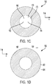
- FIGS. 1C and 1D show examples of glyphs having both a notched disk and rings surrounding the notched disk. Specifically, FIG. 1C shows a glyph 150 having both frequency diversity and polarization where frequency diversity is defined as having multiple resonant frequencies.
- the glyph 150 has a disk 160 with two notches 162, 164.
- the notches 162, 164 are disposed on opposite sides of the disk 160 and are oriented to correspond to X-polarization, but Y-polarization is doable by rotating the tag for 90° as shown in FIG. 1D .
- Two rings 170, 172 surround the notched disk 160.
- FIG. 1D illustrates another glyph 155 having both frequency diversity and polarization diversity.
- the glyph 155 has a disk 180 with two notches 182, 184.
- the notches 182, 184 are disposed on opposite sides of the disk 180.
- Two rings 190, 192 surround the notched disk 180. While the examples shown in FIGS. 1C and 1D show a disk having two notches and two rings, it is to be understood that there can be more or fewer notches and more or fewer rings.
- the disk is not notched and/or one or more of the slot rings includes an opening and/or a notch.
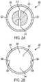
- FIG. 2A illustrates an example of a glyph 200 that includes a disk 210 having two notches 212, 214.
- the disk 210 is surrounded by a ring 220 having two notches 222, 224 completely through the ring 220.
- the notches 212, 214 in the disk 210 are in a Y-orientation and the notches 222, 224 in the ring 220 are in an X-orientation.
- the number of notches in the disk 210 and the number of notches in the ring 220 may be different.
- FIG. 2B shows a glyph 230 having a disk 240 with two notches 242, 244 in a Y-orientation.
- the disk 240 is surrounded by a ring 250 having two notches 252, 254 that do not go completely through the ring 250.
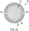
- FIG. 2C illustrates an example of a glyph 260 that includes a disk 270.
- the disk 270 is surrounded by an inner ring 280 and an outer ring 290.
- the outer ring 290 has two notches 292, 294 that go completely through the outer ring 290. While the example of FIG. 2C shows notches in the outer ring, it is to be understood that the notches could be disposed in the inner ring 280 or in the inner ring 280 and the outer ring 290.
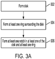
- FIG. 3A shows a process for forming a chipless patterned conductor in accordance with embodiments described herein.
- a disk is formed 302.
- At least one ring surrounding the disk is formed 304.
- One or more of a spacing between the disk and the at least one ring and a width of the at least one ring is configured to determine a characteristic resonant frequency of the glyph.
- At least one notch is formed 306 in at least one of the disk and at least one ring of the ring structure. The at least one notch is configured such that the magnitude of resonances in the glyph are dependent on polarization direction.
- the patterned conductor may be configured to operate in any frequency band including C band (4-8 GHz), X band (8-12 GHz), Ku, K and Ka (12-40 GHz), Q band (33-50), V band (50-75 GHz), and/or W band (75-110 GHz). While specific frequency ranges are included here, it is to be understood that the frequency range may be greater than 110 GHz and/or lower than 4 GHz.
- the at least one glyph is formed on a substrate and the at least one glyph with the substrate is transferred to an object, e.g., a box.
- the substrate may be a sticker that can be transferred to the object.
- the glyph is formed directly on an object.
- the glyph may be formed on a package, a paper cup, a pallet, and/or an article of clothing.
- the at least one glyph may be formed by printing the at least one glyph from a conductive material.
- the glyph may be fabricated from printed inks comprising one or more of silver and copper. In some cases, the printed inks could include one or more of nickel, carbon, carbon nanotubes, and silver nanowires.
- the glyph is fabricated by etching metal on a dielectric substrate.
- the glyph may be fabricated by etching one or more of copper and aluminum.
- the glyph may be fabricated by etching a transparent conductor such as indium-tin oxide, for example.
- the glyph is fabricated with a thermal transfer process using conductive ribbons of one or more of copper, aluminum, gold, and/or silver, for example.
- the glyph is fabricated through vapor deposition.
- the glyph may be fabricated using a sputtering and/or a thermal evaporation process.
- the substrate onto which the conductor is patterned may be a high-performance dielectric such as Taconic TLX- 8, a low cost polymer such as mylar, polyethylene tetrapthalate (PET) and/or polyethylene naphthalate (PEN,) and/or another substrate material such as polyimide, glass or paper, and/or any of the above pre-coated on the reverse side with a conductive film.
- a high-performance dielectric such as Taconic TLX- 8
- a low cost polymer such as mylar, polyethylene tetrapthalate (PET) and/or polyethylene naphthalate (PEN,)
- PET polyethylene naphthalate
- another substrate material such as polyimide, glass or paper
- the at least one glyph is formed from a conductive foil and the at least one glyph 310 is transferred to a substrate 320 as shown in FIG. 3B .
- the substrate 325 has a first side 327 and an opposing second side 329.
- a conductive layer 330 disposed on the second side 329 of the substrate 325 and the glyph 315 is transferred to the first side 327 of the substrate 325, as shown in FIG 3C .
- the conductive layer is a ground plane.
- FIGS 3D illustrate an embodiment having more than one glyph in accordance with embodiments described herein.
- FIG. 3D shows a substrate layer 362 having a first side 364 and an opposing second side 366.
- a first glyph 352 is disposed on the first side 364 of the substrate layer 362 and a second glyph 372 is disposed on the second side 366 of the substrate layer 362.
- FIG. 3E shows another example having more than one glyph.
- a first glyph 380 is disposed on a first side 392 of a first substrate layer 382.
- a conductive layer 384 is disposed between a second side 392 of the first substrate layer 392 and a first side 394 of a second substrate layer 386.
- a second glyph 388 is disposed on the second side 396 of the second substrate layer 386.
- FIGS. 4A and 4B show a more detailed view of a hybrid glyph in accordance with embodiments described herein.
- the glyph 400 has a radius, R, in a range of about 1.5 mm to about 2.5 mm. According to various implementations, R is about 1.5 mm. In some cases, R is less than 1.5 mm or greater than 2.5 mm.
- the disk 420 has a radius, R D , in a range of about 0.4 mm to about 0.8 mm. According to various implementations, R D is about 0.45 mm.
- the disk has a first notch 422 and a second notch 424.
- the first notch 422 has a length, L 1 and a width W N1 .
- the second notch 424 has a length, L 2 and a width W N2 .
- W N1 is substantially equal to W N2 and/or L 1 is substantially equal to L 2 . In some cases, L 1 is a different value than L 2 and/or W N1 is a different value than W N2 .
- L 1 and L 2 are in a range of about 0.4 mm to about 0.795 mm. According to various implementations, L 1 and/or L 2 is about 0.405 mm. According to embodiments described herein, W N1 and W N2 are in a range of about 0.1 mm to about 0.6 mm. According to various implementations, W N1 and/or W N2 is about 0.05 mm.
- a first ring 430 and a second ring 432 surround the disk 420.
- the first ring 430 has a width, W R1 in a range of about 0.05 mm to about 0.1 mm. According to various implementations, W R1 is about 0.105.
- the second ring 432 has a width, W R2 in a range of about 0.04 mm to about 0.08 mm. According to various implementations, W R2 is about 0.0495. In some cases, W R1 is substantially equal to W R2 .
- a first gap has a width, W G1 in a range of about 0.025 mm to about 0.05 mm.
- a second gap has a width, W G2 in a range of about 0.018 mm to about 0.03 mm. According to various implementations, W G1 is about 0.025 mm and/or W G2 is about 0.018 mm. In some cases, W G1 is substantially equal to W G2 .
- At least one of the dimensions of the glyph are selected according to an optimization process.
- the dimensions may be selected to have a resonance at a specific frequency. This may be accomplished by determining one or more of an approximate radius of the disk using Equation (1), where widths of the notches, and/or the widths of the rings are determined through an optimization process.
- Equation (1) 1.8412 c 2 ⁇ f r ⁇ r
- c is the speed of light in free space
- f r is the design resonant frequency
- ⁇ r is the dielectric constant of the substrate used for design.
- the glyph is then designed using the estimated dimensions.
- a simulation is performed using available commercial electromagnetic simulation tools and the frequency behavior of the design is monitored.
- the dimensions are then tuned to get resonance at the desired frequencies.
- FIG. 5 shows a simulation setup 500 for the hybrid chipless patterned conductor in accordance with embodiments described herein.
- a linearly polarized plane wave 520 is used for excitation of the patterned conductor 510.
- one or more probes may located at a specified distance away from the patterned conductor 510.
- the probes may be located about 10 cm away from the patterned conductor 510.
- the tag is disposed on a substrate 530.
- the tag may be disposed on a 5 mil Taconic TLX- 8 substrate with permittivity, ⁇ r , of about 2.55 and loss, ⁇ , of about 0.0017.
- An optimization process may be run to optimize the size of the rings and the notched disk to have resonances at the desired frequency.
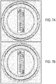
- FIG. 7A illustrates the surface current distribution at about 57 GHz of the configuration shown in FIG. 1A.
- FIG. 7B illustrates the surface current distribution at about 64 GHz of the configuration shown in FIG. 1A.
- FIG. 7A and 7B show the relationship between the coupling of the adjacent slots and the resonances. It can be observed that the current density vector of adjacent slots is opposite and generates magnetic resonance. The width of the slots influences the coupling strength and the resonance frequency. The smaller slot width is shifting down the resonance frequency while a larger slot width results in shifting up the resonances.
- FIG. 8 shows the simulation results of the backscattered electric field of the patterned conductor of FIG. 1B excited by an X-polarized plane for notches oriented horizontally 810 as in FIG. 1C and notches rotated 90° and oriented vertically 820 as in FIG. 1D .
- the surface current distribution at about 60 GHz of the configuration shown in FIG. 1B is shown in FIG. 9 .
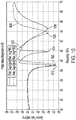
- FIG. 10 shows the simulation results of the backscattered electric field for a patterned conductor having a glyph with notches that are perpendicular 1010 to the direction of the incident electric field (90° rotation) as in FIG. 1C and for a patterned conductor having a glyph with notches that are oriented the same direction 1020 as the incident electric field (180° rotation) as in FIG. 1D .
- the notches are oriented perpendicularly to the incident electric field
- three resonances 1012, 1014, 1016 are observed in the monitored frequency band.
- the resonances at 57 GHz 1012 and at 64 GHz 1016 are due to the rings and the resonance observed at 60 GHz 1014 is the effect of the notched disk.
- the resonances 1022, 1026 that are due to the rings are observed.
- Binary data can be coded by the presence or the absence of the resonances.
- the removal of a notch and/or the removal of a ring can be denoted as logic "0" where the appearance of a notch is denoted as logic "1".
- each glyph of the patterned conductor can represent 3 bits for each of the three resonances.
- the number of combinations that can be encoded for each glyph using both frequency and polarization diversity is equal to 8.
- the minimum number of glyphs, considering enough separation between each, is 40 glyphs. Therefore, the tag has the ability to store 120 bits of data.
- FIGS. 11A-11C show the surface current distribution at the resonant frequencies for the hybrid configuration shown in FIG. 1C where the notches are oriented perpendicularly to the incident electric field. Specifically, FIG. 11A illustrates the surface current distribution at about 57 GHz, FIG. 11B illustrates the surface current distribution at about 60 GHz, and FIG. 11C illustrates the surface current distribution at about 64 GHz.
- a chipless RFID tag comprises an array of patterned conductors.
- FIG. 12 illustrates an example array of patterned conductors.
- the array of patterned conductors may have one or more glyphs of varying ring sizes, ring spacings, and/or notch orientations.
- FIG. 13 shows a chipless RFID system 1300 that is configured to read the one or more patterned conductors.
- a transmitter configured to transmit an electromagnetic radiation signal towards the patterned conductor.
- the system includes a receiver configured to receive a backscattered signal.
- a processor coupled to the receiver is configured to associate the backscattered signal with a digital signature using information stored in a storage device 1340.
- the RFID system 1300 may include one or more network interfaces 1350 for communicating with other devices via a network.
- the system may include other input/output devices 1360 that enable user interaction with the system 1300 (e.g., display, keyboard, mouse, speakers, buttons, etc.
- FIG. 13 is a high level representation of possible components of a RFID system for illustrative purposes. It is to be understood that the RFID system shown in FIG. 13 may contain other components.
Landscapes
- Engineering & Computer Science (AREA)
- Physics & Mathematics (AREA)
- General Physics & Mathematics (AREA)
- Theoretical Computer Science (AREA)
- Computer Hardware Design (AREA)
- Microelectronics & Electronic Packaging (AREA)
- Computer Networks & Wireless Communication (AREA)
- Electromagnetism (AREA)
- Health & Medical Sciences (AREA)
- General Health & Medical Sciences (AREA)
- Toxicology (AREA)
- Artificial Intelligence (AREA)
- Computer Vision & Pattern Recognition (AREA)
- Signal Processing (AREA)
- Control Of Motors That Do Not Use Commutators (AREA)
- Aerials With Secondary Devices (AREA)
Abstract
Description
- The present disclosure is directed to radio frequency identification (RFID).
- The radio frequency identification (RFID) tag is a type of identification device. When interrogated by a reading device which is also called an interrogator, RFID tags reflect or retransmit a radio frequency signal to return an encoded identification (ID) to the interrogator. RFID tag devices may be of two basic types. Chipped RFID tags include a microchip that stores data. Chipless RFID tags do not contain a microchip but instead rely on magnetic materials or transistorless thin film circuits to store data.
- Embodiments described herein involve a chipless patterned conductor comprising one or more glyphs. Each glyph comprises a disk and a ring structure comprising at least one ring surrounding the disk. One or more of a spacing between the disk and the at least one ring and a width of the at least one ring is configured to determine a characteristic resonant frequency of the glyph. At least one notch is disposed in at least one of the disk and at least one ring of the ring structure. The at least one notch is configured such that the magnitude of resonances in the glyph are dependent on polarization direction.
- A method of forming a chipless patterned conductor comprises forming at least one glyph. The at least one glyph is formed by forming a disk and forming a ring structure comprising least one ring surrounding the disk. One or more of a spacing between the disk and the at least one ring and a width of the at least one ring is configured to determine a characteristic resonant frequency of the glyph. At least one notch is formed in at least one of the disk and at least one ring of the ring structure. The at least one notch is configured such that the magnitude of resonances in the glyph are dependent on polarization direction.
- A system for reading a patterned conductor comprises
21. A system for reading a patterned conductor comprising a transmitter configured to transmit an electromagnetic radiation signal towards the patterned conductor, the patterned conductor comprising one or more glyphs. Each glyph comprises a disk and a ring structure comprising at least one ring surrounding the disk. One or more of a spacing between the disk and the at least one ring and a width of the at least one ring is configured to determine a characteristic resonant frequency of the glyph. At least one notch is disposed in at least one of the disk and at least one ring of the ring structure. The at least one notch is configured such that the magnitude of resonances in the glyph are dependent on polarization direction. Each glyph is configured to backscatter at least a portion of the electromagnetic radiation based on the characteristic resonant frequency and the magnitude of resonances. A receiver is configured to receive a backscattered signal. A processor is configured to associate the backscattered signal with a digital signature. - The above summary is not intended to describe each embodiment or every implementation. A more complete understanding will become apparent and appreciated by referring to the following detailed description and claims in conjunction with the accompanying drawings.
-
-
FIGS. 1A and 1B illustrate example glyphs in accordance with embodiments described herein; -
FIGS. 1C and 1D show examples of hybrid glyphs having both a notched disk and rings surrounding the notched disk in accordance with embodiments described herein; -
FIGS. 2A-2C illustrate examples of a glyph in which one or more of the rings has at least one notch in accordance with embodiments described herein; -
FIG. 3A shows a process for forming a chipless patterned conductor in accordance with embodiments described herein; -
FIGS. 3B and 3C illustrate examples of a glyph disposed on a substrate in accordance with embodiments described herein; -
FIGS. 3D and 3E illustrate embodiments having more than one glyph in accordance with embodiments described herein; -
FIGS. 4A and 4B show a more detailed view of a hybrid glyph in accordance with embodiments described herein; -
FIG. 5 shows a simulation setup for the hybrid chipless patterned conductor in accordance with embodiments described herein; -
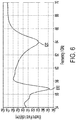
FIG. 6 illustrates deep notches that are observed at the resonance frequencies of the ring resonators in accordance with embodiments described herein; -
FIG. 7A shows the surface current distribution at about 57 GHz of the configuration shown inFIG. 1A in accordance with embodiments described herein; -
FIG. 7B illustrates the surface current distribution at about 64 GHz of the configuration shown inFIG. 1A in accordance with embodiments described herein; -
FIG. 8 shows the simulation results of the backscattered electric field of the patterned conductor ofFIG. 1B excited by an X-polarized plane for notches oriented horizontally as inFIG. 1C and notches rotated 90° and oriented vertically as inFIG. 1D in accordance with embodiments described herein; -
FIG. 9 illustrates the surface current distribution at about 60 GHz of the configuration shown inFIG. 1B in accordance with embodiments described herein; -
FIG. 10 show the simulation results of the backscattered electric field for a patterned conductor having notches are perpendicular to the direction of the incident electric field (90° rotation) as inFIG. 1C and for a patterned conductor having notches that are oriented the same direction as the incident electric field (180° rotation) as inFIG. 1D in accordance with embodiments described herein; -
FIG. 11A illustrates the surface current distribution at about 57 GHz for the hybrid glyph in accordance with embodiments described herein; -
FIG. 11B illustrates the surface current distribution at about 60 GHz for the hybrid glyph in accordance with embodiments described herein; -
FIG. 11C illustrates the surface current distribution at about 64 GHz for the hybrid glyph in accordance with embodiments described herein; -
FIG. 12 illustrates an example array of glyphs in accordance with embodiments described herein. -
FIG. 13 shows a block diagram of an RFID system capable of implementing embodiments described herein. - The figures are not necessarily to scale. Like numbers used in the figures refer to like components. However, it will be understood that the use of a number to refer to a component in a given figure is not intended to limit the component in another figure labeled with the same number.
- Radio frequency identification (RFID) technologies have many different applications. Chipless RFID is a wireless data capturing technique applying electromagnetic waves to extract the encoded data in a tag. Chipless RFID tags have the potential to replace barcode. There is potential to enhance the performance of chipless RFID in terms of increasing encoding capacity, simplifying fabrication, and lowering costs.
- According to embodiments described herein, the coding efficiency of chipless RFID may be improved by using a hybrid encoding technique by combining polarization sensitivity with multiple frequency encoding in a single conductive glyph. According to embodiments described herein this is done in the millimeter-wave (mm-wave) regime, though the technique is not limited to this frequency range and higher or lower frequencies can also be used. One motivation of this design is to improve the coding efficiency of chipless RFID tags. In general, there are different methods to increase the coding capacity in a RFID tag design process. Some embodiments involve the integration of multiple simple glyphs where each glyph can hold few bits. Increasing the capacity of each single glyph increases the capacity of the full tag by extension.
- According to embodiments described herein data can be encoded a within a frequency band by creating some resonances in the backscattered signal at certain frequencies. Embodiments described herein are based on the concept of slot ring resonators where all rings have a common center creating a concentric configuration. To do so, the slot ring resonators with various diameters are designed to encode different frequency signatures in which each signature represents a bit. Harmonic resonances are not observed in the backscattered signal as the current paths of the even and odd harmonics are canceled due to the symmetric configuration of the design. Therefore, the complete frequency band can be used to encode data. To add polarization diversity to the designed tag, two symmetric rectangular notches are created in the inner circular disk and/or in one or more of the rings. According to embodiments described herein, the hybrid tag may not have a ground plane and therefore the field lines are not concentrated into the substrate.
- A patterned conductor comprises one or more glyphs in accordance with embodiments described herein. The glyph is a patterned conductive material disposed on a dielectric substrate. According to some embodiments, the reverse side of the substrate has a continuous conductor (e.g., a "ground plane").
FIG. 1A illustrates an example of aglyph 100. Theglyph 100 includes adisk 110 having tworings -
FIG. 1B illustrates an example of aglyph 105 in accordance with embodiments described herein. Theglyph 105 ofFIG. 1B includes adisk 130 with twonotches notches - According to various embodiments, a patterned conductor can be printed that is sensitive to both polarization and frequency. The hybrid (polarization-and frequency) configuration may enhance the coding efficiency and working in the mm-wave regime brings the advantage of a smaller glyph size. According to embodiments described herein, the patterned conductor comprises one or more glyphs that are placed in a credit card size (e.g., 85.60 × 53.98 mm) tag to increase the total coding efficiency. Both larger and smaller size tags are also realizable. In some cases, the hybrid tag doesn't need a ground plane which results in simplifying and reducing the cost of fabrication. Embodiments described herein may involve a patterned conductor that can radiate without a ground plane because the rings serve as counter electrodes for the central notched disk and the wave is guided between two strips or within the notch width.
- According to embodiments described herein, a simple glyph includes a notched circular patch surrounded by a slot ring.
FIGS. 1C and 1D show examples of glyphs having both a notched disk and rings surrounding the notched disk. Specifically,FIG. 1C shows aglyph 150 having both frequency diversity and polarization where frequency diversity is defined as having multiple resonant frequencies. - . The
glyph 150 has adisk 160 with twonotches notches disk 160 and are oriented to correspond to X-polarization, but Y-polarization is doable by rotating the tag for 90° as shown inFIG. 1D . Two rings 170, 172 surround the notcheddisk 160.FIG. 1D illustrates anotherglyph 155 having both frequency diversity and polarization diversity. Theglyph 155 has adisk 180 with twonotches notches disk 180. Two rings 190, 192 surround the notcheddisk 180. While the examples shown inFIGS. 1C and 1D show a disk having two notches and two rings, it is to be understood that there can be more or fewer notches and more or fewer rings. - According to some embodiments, the disk is not notched and/or one or more of the slot rings includes an opening and/or a notch.
FIG. 2A illustrates an example of aglyph 200 that includes adisk 210 having twonotches disk 210 is surrounded by aring 220 having twonotches ring 220. In this example thenotches disk 210 are in a Y-orientation and thenotches ring 220 are in an X-orientation. In some configurations, the number of notches in thedisk 210 and the number of notches in thering 220 may be different.FIG. 2B shows aglyph 230 having adisk 240 with twonotches disk 240 is surrounded by aring 250 having twonotches ring 250.FIG. 2C illustrates an example of aglyph 260 that includes adisk 270. Thedisk 270 is surrounded by aninner ring 280 and anouter ring 290. Theouter ring 290 has twonotches outer ring 290. While the example ofFIG. 2C shows notches in the outer ring, it is to be understood that the notches could be disposed in theinner ring 280 or in theinner ring 280 and theouter ring 290. -
FIG. 3A shows a process for forming a chipless patterned conductor in accordance with embodiments described herein. A disk is formed 302. At least one ring surrounding the disk is formed 304. One or more of a spacing between the disk and the at least one ring and a width of the at least one ring is configured to determine a characteristic resonant frequency of the glyph. At least one notch is formed 306 in at least one of the disk and at least one ring of the ring structure. The at least one notch is configured such that the magnitude of resonances in the glyph are dependent on polarization direction. - The patterned conductor may be configured to operate in any frequency band including C band (4-8 GHz), X band (8-12 GHz), Ku, K and Ka (12-40 GHz), Q band (33-50), V band (50-75 GHz), and/or W band (75-110 GHz). While specific frequency ranges are included here, it is to be understood that the frequency range may be greater than 110 GHz and/or lower than 4 GHz.
- According to embodiments described herein, the at least one glyph is formed on a substrate and the at least one glyph with the substrate is transferred to an object, e.g., a box. For example, the substrate may be a sticker that can be transferred to the object. According to various implementations, the glyph is formed directly on an object. For example, the glyph may be formed on a package, a paper cup, a pallet, and/or an article of clothing. The at least one glyph may be formed by printing the at least one glyph from a conductive material. For example, the glyph may be fabricated from printed inks comprising one or more of silver and copper. In some cases, the printed inks could include one or more of nickel, carbon, carbon nanotubes, and silver nanowires. According to various configurations, a post-printing annealing process takes place. According to various embodiments, the glyph is fabricated by etching metal on a dielectric substrate. For example, the glyph may be fabricated by etching one or more of copper and aluminum. The glyph may be fabricated by etching a transparent conductor such as indium-tin oxide, for example. In some implementations, the glyph is fabricated with a thermal transfer process using conductive ribbons of one or more of copper, aluminum, gold, and/or silver, for example. According to some embodiments, the glyph is fabricated through vapor deposition. For example, the glyph may be fabricated using a sputtering and/or a thermal evaporation process. In any of these processes the substrate onto which the conductor is patterned may be a high-performance dielectric such as Taconic TLX- 8, a low cost polymer such as mylar, polyethylene tetrapthalate (PET) and/or polyethylene naphthalate (PEN,) and/or another substrate material such as polyimide, glass or paper, and/or any of the above pre-coated on the reverse side with a conductive film.
- While various techniques are described herein that can be used to form the patterned conductor, it is to be understood that any technique can be used alone or in combination with any other process.
- In some configurations, the at least one glyph is formed from a conductive foil and the at least one
glyph 310 is transferred to asubstrate 320 as shown inFIG. 3B . According to various implementations, thesubstrate 325 has afirst side 327 and an opposingsecond side 329. Aconductive layer 330 disposed on thesecond side 329 of thesubstrate 325 and theglyph 315 is transferred to thefirst side 327 of thesubstrate 325, as shown inFIG 3C . According to various configurations, the conductive layer is a ground plane. -
FIGS 3D illustrate an embodiment having more than one glyph in accordance with embodiments described herein.FIG. 3D shows asubstrate layer 362 having afirst side 364 and an opposingsecond side 366. Afirst glyph 352 is disposed on thefirst side 364 of thesubstrate layer 362 and a second glyph 372 is disposed on thesecond side 366 of thesubstrate layer 362.FIG. 3E shows another example having more than one glyph. Afirst glyph 380 is disposed on afirst side 392 of afirst substrate layer 382. Aconductive layer 384 is disposed between asecond side 392 of thefirst substrate layer 392 and afirst side 394 of asecond substrate layer 386. Asecond glyph 388 is disposed on thesecond side 396 of thesecond substrate layer 386. -
FIGS. 4A and 4B show a more detailed view of a hybrid glyph in accordance with embodiments described herein. Theglyph 400 has a radius, R, in a range of about 1.5 mm to about 2.5 mm. According to various implementations, R is about 1.5 mm. In some cases, R is less than 1.5 mm or greater than 2.5 mm. - The
disk 420 has a radius, RD, in a range of about 0.4 mm to about 0.8 mm. According to various implementations, RD is about 0.45 mm. In this example, the disk has afirst notch 422 and asecond notch 424. Thefirst notch 422 has a length, L1 and a width WN1. Thesecond notch 424 has a length, L2 and a width WN2. According to embodiments described herein WN1 is substantially equal to WN2 and/or L1 is substantially equal to L2. In some cases, L1 is a different value than L2 and/or WN1 is a different value than WN2. According to embodiments described herein L1 and L2 are in a range of about 0.4 mm to about 0.795 mm. According to various implementations, L1 and/or L2 is about 0.405 mm. According to embodiments described herein, WN1 and WN2 are in a range of about 0.1 mm to about 0.6 mm. According to various implementations, WN1 and/or WN2 is about 0.05 mm. - A
first ring 430 and asecond ring 432 surround thedisk 420. Thefirst ring 430 has a width, WR1 in a range of about 0.05 mm to about 0.1 mm. According to various implementations, WR1 is about 0.105. Thesecond ring 432 has a width, WR2 in a range of about 0.04 mm to about 0.08 mm. According to various implementations, WR2 is about 0.0495. In some cases, WR1 is substantially equal to WR2. A first gap has a width, WG1 in a range of about 0.025 mm to about 0.05 mm. A second gap has a width, WG2 in a range of about 0.018 mm to about 0.03 mm. According to various implementations, WG1 is about 0.025 mm and/or WG2 is about 0.018 mm. In some cases, WG1 is substantially equal to WG2. - According to embodiments described herein, at least one of the dimensions of the glyph are selected according to an optimization process. For example, the dimensions may be selected to have a resonance at a specific frequency. This may be accomplished by determining one or more of an approximate radius of the disk using Equation (1), where widths of the notches, and/or the widths of the rings are determined through an optimization process.

- Here, c is the speed of light in free space, fr is the design resonant frequency and εr is the dielectric constant of the substrate used for design.
- The glyph is then designed using the estimated dimensions. A simulation is performed using available commercial electromagnetic simulation tools and the frequency behavior of the design is monitored. The dimensions are then tuned to get resonance at the desired frequencies.
-
FIG. 5 shows asimulation setup 500 for the hybrid chipless patterned conductor in accordance with embodiments described herein. A linearlypolarized plane wave 520 is used for excitation of the patternedconductor 510. To monitor the backscattered electric field, far-field one or more probes may located at a specified distance away from the patternedconductor 510. For example, the probes may be located about 10 cm away from the patternedconductor 510. The tag is disposed on asubstrate 530. For example, the tag may be disposed on a 5 mil Taconic TLX- 8 substrate with permittivity, εr, of about 2.55 and loss, δ, of about 0.0017. An optimization process may be run to optimize the size of the rings and the notched disk to have resonances at the desired frequency. - When a plane wave impinges the rings shown in
FIG. 1A , a frequency selective behavior with peaks followed by deep notches are observed at the resonance frequencies of the ring resonators as depicted inFIG. 6 where twodeep notches first resonance 610 occurs at about 57 GHz which relates to thebigger ring 122. Thesecond resonance 620, which is due to thesmaller ring 120 happens at about 64 GHz. The innercircular disk 110 falls outside the desired frequency band, therefore those two resonances are just due to the rings. - The surface current distribution at about 57 GHz of the configuration shown in
FIG. 1A is illustrated inFIG. 7A. FIG. 7B illustrates the surface current distribution at about 64 GHz of the configuration shown inFIG. 1A.FIG. 7A and 7B show the relationship between the coupling of the adjacent slots and the resonances. It can be observed that the current density vector of adjacent slots is opposite and generates magnetic resonance. The width of the slots influences the coupling strength and the resonance frequency. The smaller slot width is shifting down the resonance frequency while a larger slot width results in shifting up the resonances. -
FIG. 8 shows the simulation results of the backscattered electric field of the patterned conductor ofFIG. 1B excited by an X-polarized plane for notches oriented horizontally 810 as inFIG. 1C and notches rotated 90° and oriented vertically 820 as inFIG. 1D . The surface current distribution at about 60 GHz of the configuration shown inFIG. 1B is shown inFIG. 9 . -
FIG. 10 shows the simulation results of the backscattered electric field for a patterned conductor having a glyph with notches that are perpendicular 1010 to the direction of the incident electric field (90° rotation) as inFIG. 1C and for a patterned conductor having a glyph with notches that are oriented thesame direction 1020 as the incident electric field (180° rotation) as inFIG. 1D . In thecase 1010 where the notches are oriented perpendicularly to the incident electric field, threeresonances GHz 1016 are due to the rings and the resonance observed at 60GHz 1014 is the effect of the notched disk. In thecase 1020 where the notches are oriented in the same direction as the incident electric field, only theresonances - Binary data can be coded by the presence or the absence of the resonances. For example, the removal of a notch and/or the removal of a ring can be denoted as logic "0" where the appearance of a notch is denoted as logic "1". This is just one example of how logic can be encoded in the patterned conductor. Here, it is shown that each glyph of the patterned conductor can represent 3 bits for each of the three resonances. The number of combinations that can be encoded for each glyph using both frequency and polarization diversity is equal to 8. In a credit card size chipless tag the minimum number of glyphs, considering enough separation between each, is 40 glyphs. Therefore, the tag has the ability to store 120 bits of data.
-
FIGS. 11A-11C show the surface current distribution at the resonant frequencies for the hybrid configuration shown inFIG. 1C where the notches are oriented perpendicularly to the incident electric field. Specifically,FIG. 11A illustrates the surface current distribution at about 57 GHz,FIG. 11B illustrates the surface current distribution at about 60 GHz, andFIG. 11C illustrates the surface current distribution at about 64 GHz. - According to embodiments described herein, a chipless RFID tag comprises an array of patterned conductors.
FIG. 12 illustrates an example array of patterned conductors. The array of patterned conductors may have one or more glyphs of varying ring sizes, ring spacings, and/or notch orientations. -
FIG. 13 shows achipless RFID system 1300 that is configured to read the one or more patterned conductors. A transmitter configured to transmit an electromagnetic radiation signal towards the patterned conductor. The system includes a receiver configured to receive a backscattered signal. A processor coupled to the receiver is configured to associate the backscattered signal with a digital signature using information stored in astorage device 1340. TheRFID system 1300 may include one ormore network interfaces 1350 for communicating with other devices via a network. The system may include other input/output devices 1360 that enable user interaction with the system 1300 (e.g., display, keyboard, mouse, speakers, buttons, etc.FIG. 13 is a high level representation of possible components of a RFID system for illustrative purposes. It is to be understood that the RFID system shown inFIG. 13 may contain other components. - Unless otherwise indicated, all numbers expressing feature sizes, amounts, and physical properties used in the specification and claims are to be understood as being modified in all instances by the term "about." Accordingly, unless indicated to the contrary, the numerical parameters set forth in the foregoing specification and attached claims are approximations that can vary depending upon the desired properties sought to be obtained by those skilled in the art utilizing the teachings disclosed herein. The use of numerical ranges by endpoints includes all numbers within that range (e.g. 1 to 5 includes 1, 1.5, 2, 2.75, 3, 3.80, 4, and 5) and any range within that range.
- The various embodiments described above may be implemented using circuitry and/or software modules that interact to provide particular results. One of skill in the computing arts can readily implement such described functionality, either at a modular level or as a whole, using knowledge generally known in the art. For example, the flowcharts illustrated herein may be used to create computer-readable instructions/code for execution by a processor. Such instructions may be stored on a computer-readable medium and transferred to the processor for execution as is known in the art.
- The foregoing description of the example embodiments have been presented for the purposes of illustration and description. It is not intended to be exhaustive or to limit the inventive concepts to the precise form disclosed. Many modifications and variations are possible in light of the above teachings. Any or all features of the disclosed embodiments can be applied individually or in any combination, not meant to be limiting but purely illustrative. It is intended that the scope be limited by the claims appended herein and not with the detailed description.
Claims (23)
- A chipless patterned conductor, comprising:
one or more glyphs, each glyph comprising:a disk;a ring structure comprising at least one ring surrounding the disk, wherein one or more of a spacing between the disk and the at least one ring and a width of the at least one ring is configured to determine a characteristic resonant frequency of the glyph; andat least one notch in at least one of the disk and at least one ring of the ring structure, the at least one notch configured such that the magnitude of resonances in the glyph are dependent on polarization direction. - The chipless patterned conductor of claim 1, wherein the ring structure is configured to resonate in a band of about 40 GHz to about 75-110 GHz.
- The chipless patterned conductor of claim 1, wherein the ring structure comprises a first ring and a second ring.
- The chipless patterned conductor of claim 3, wherein a width of the first ring is different than a width of the second ring
- The chipless patterned conductor of claim 3, wherein a width of the first ring is substantially the same as the width of the second ring.
- The chipless patterned conductor of claim 3, wherein a spacing between the first ring and the disk is different than a spacing between the second ring and the disk.
- The chipless patterned conductor of claim 1, wherein the disk has two notches.
- The chipless patterned conductor of claim 7, wherein the two notches are on opposite sides of the disk.
- The chipless patterned conductor of claim 1, further comprising:a ground plane; anda dielectric layer disposed between the one or more glyphs and the ground plane.
- The chipless patterned conductor of claim 1, wherein the ring structure comprises a first ring and a second ring surrounding the first ring, the second ring configured to serve as a counter electrode for the first ring and the disk.
- The chipless patterned conductor of claim 1, wherein the one or more glyphs comprises a plurality of glyphs.
- The chipless patterned conductor of claim 11, wherein a first glyph of the plurality of glyphs has one or more of first ring configuration and a first notch configuration and the second glyph of the plurality of glyphs has one or more of a second ring configuration different than the first ring configurations and a second notch configuration different than the first notch configuration.
- The chipless patterned conductor of claim 1, wherein the ring structure comprises a first ring and a second ring surrounding the first ring and the at least one notch is disposed in the second ring.
- A method of forming a chipless patterned conductor, comprising:
forming at least one glyph, comprising:forming a disk;forming a ring structure comprising least one ring surrounding the disk, wherein one or more of a spacing between the disk and the at least one ring and a width of the at least one ring is configured to determine a characteristic resonant frequency of the glyph; andforming at least one notch in at least one of the disk and at least one ring of the ring structure, the at least one notch configured such that the magnitude of resonances in the glyph are dependent on polarization direction. - The method of claim 14, further comprising forming the at least one glyph on a substrate and transferring the at least one glyph to an object.
- The method of claim 14, wherein forming the at least one glyph comprises forming the at least one glyph directly on an object.
- The method of claim 14, wherein forming the at least one glyph comprises printing the at least one glyph from a conductive material.
- The method of claim 14, wherein forming the at least one glyph comprises:forming the at least one glyph from a conductive foil; andtransferring the at least one glyph to a substrate.
- The method of claim 18, wherein the substrate has a first side and an opposite second side and a conductive layer disposed on the second side of the substrate, wherein transferring the at least one glyph to the substrate comprises transferring the at least one glyph to the first side of the substrate.
- The method of claim 18, wherein the substrate has a first side and an opposite second side and the at least one glyph comprises a first glyph and a second glyph, wherein the first glyph is disposed on the first side of the substrate and the second glyph is disposed on the second side of the substrate.
- The method of claim 20, wherein the substrate comprises a first substrate layer and a second substrate layer and a conductive layer is disposed between the first substrate layer and the second substrate layer.
- The method of claim 14, further comprising:depositing a conductive ground plane on a substrate;depositing a dielectric layer on the conductive ground plane; andforming the at least one glyph on the dielectric layer.
- A system for reading a patterned conductor comprising:a transmitter configured to transmit an electromagnetic radiation signal towards the patterned conductor, the patterned conductor comprising one or more glyphs each glyph comprising:a disk;a ring structure comprising at least one ring surrounding the disk, wherein one or more of a spacing between the disk and the at least one ring and a width of the at least one ring is configured to determine a characteristic resonant frequency of the glyph; andat least one notch in at least one of the disk and at least one ring of the ring structure, the at least one notch configured such that the magnitude of resonances in the glyph are dependent on polarization direction, wherein each glyph is configured to backscatter at least a portion of the electromagnetic radiation based on the characteristic resonant frequency and the magnitude of resonances;a receiver configured to receive a backscattered signal; anda processor configured to associate the backscattered signal with a digital signature.
Applications Claiming Priority (1)
| Application Number | Priority Date | Filing Date | Title |
|---|---|---|---|
| US16/515,628 US11163967B2 (en) | 2019-07-18 | 2019-07-18 | Chipless RFID tag using hybrid coding |
Publications (2)
| Publication Number | Publication Date |
|---|---|
| EP3767539A1 true EP3767539A1 (en) | 2021-01-20 |
| EP3767539B1 EP3767539B1 (en) | 2023-08-09 |
Family
ID=71143611
Family Applications (1)
| Application Number | Title | Priority Date | Filing Date |
|---|---|---|---|
| EP20182119.6A Active EP3767539B1 (en) | 2019-07-18 | 2020-06-24 | Chipless rfid tag using hybrid coding |
Country Status (6)
| Country | Link |
|---|---|
| US (1) | US11163967B2 (en) |
| EP (1) | EP3767539B1 (en) |
| JP (1) | JP7419170B2 (en) |
| KR (1) | KR102639845B1 (en) |
| CN (1) | CN112241773B (en) |
| TW (1) | TWI836095B (en) |
Families Citing this family (8)
| Publication number | Priority date | Publication date | Assignee | Title |
|---|---|---|---|---|
| CN114258544A (en) * | 2019-08-26 | 2022-03-29 | 柯尼卡美能达株式会社 | Label (R) |
| JP2021089725A (en) * | 2019-11-27 | 2021-06-10 | コニカミノルタ株式会社 | tag |
| CN112241776B (en) * | 2020-09-04 | 2022-06-10 | 浙江大学 | Groove type ultra-wideband depolarized chipless RFID (radio frequency identification) tag |
| US12393822B2 (en) * | 2021-05-13 | 2025-08-19 | Board Of Trustees Of Michigan State University | Harmonic RF tag for wireless measurement of multiple products |
| US11856419B2 (en) | 2021-08-17 | 2023-12-26 | Xerox Corporation | Method and system for commissioning environmental sensors |
| US11595226B1 (en) | 2021-08-17 | 2023-02-28 | Xerox Corporation | Method and system for collecting sensor data in buildings |
| US12114386B2 (en) | 2021-08-17 | 2024-10-08 | Xerox Corporation | Building environmental sensor method and system for collecting data from same |
| US20250322199A1 (en) * | 2024-04-11 | 2025-10-16 | Iconex Llc | Chipless RFID-Enabled Liner Free Labels and Rolls of Liner Free Labels |
Citations (2)
| Publication number | Priority date | Publication date | Assignee | Title |
|---|---|---|---|---|
| US20130015248A1 (en) * | 2010-02-11 | 2013-01-17 | Universite De Savoie | Chipless passive rfid tag |
| US20180114041A1 (en) * | 2015-04-13 | 2018-04-26 | Rfid Technologies Pty Ltd | Rfid tag and reader |
Family Cites Families (12)
| Publication number | Priority date | Publication date | Assignee | Title |
|---|---|---|---|---|
| US7842004B2 (en) * | 2007-10-31 | 2010-11-30 | Codman & Shurtleff, Inc. | Wireless pressure setting indicator |
| US7843317B2 (en) * | 2008-03-05 | 2010-11-30 | International Business Machines Corporation | Environmentally sensitive electronic device |
| KR101120957B1 (en) * | 2010-06-25 | 2012-03-05 | 건국대학교 산학협력단 | Chipless rfid tag |
| JP5724671B2 (en) | 2011-03-22 | 2015-05-27 | 株式会社村田製作所 | Antenna device, RFID tag, and communication terminal device |
| US9690962B2 (en) * | 2014-01-10 | 2017-06-27 | Vdw Design, Llc | Radio-frequency identification tags |
| CN106295765B (en) * | 2016-08-12 | 2023-08-22 | 华南理工大学 | Ultra-wideband polarization-variable chipless RFID tag |
| CN106486739A (en) * | 2016-11-04 | 2017-03-08 | 华南理工大学 | A kind of dual polarization chipless RFID label antenna based on coaxial straight-flanked ring |
| WO2018218313A1 (en) | 2017-06-02 | 2018-12-06 | Monash University | Improved chipless rfid system and method |
| CN208705916U (en) | 2018-01-26 | 2019-04-05 | 同济大学 | A kind of chipless RFID electronic tag expanding information capacity |
| CN108682969A (en) * | 2018-03-16 | 2018-10-19 | 南京理工大学 | A kind of anti-metal RFID tag of passive chipless |
| CN108629398A (en) * | 2018-05-14 | 2018-10-09 | 北京邮电大学 | A kind of Chip-free label structure |
| CN109902788A (en) * | 2019-01-30 | 2019-06-18 | 南京理工大学 | A CSRR-based chipless RFID tag |
-
2019
- 2019-07-18 US US16/515,628 patent/US11163967B2/en active Active
-
2020
- 2020-06-15 TW TW109120084A patent/TWI836095B/en active
- 2020-06-16 CN CN202010548486.8A patent/CN112241773B/en active Active
- 2020-06-17 KR KR1020200073645A patent/KR102639845B1/en active Active
- 2020-06-17 JP JP2020104341A patent/JP7419170B2/en active Active
- 2020-06-24 EP EP20182119.6A patent/EP3767539B1/en active Active
Patent Citations (2)
| Publication number | Priority date | Publication date | Assignee | Title |
|---|---|---|---|---|
| US20130015248A1 (en) * | 2010-02-11 | 2013-01-17 | Universite De Savoie | Chipless passive rfid tag |
| US20180114041A1 (en) * | 2015-04-13 | 2018-04-26 | Rfid Technologies Pty Ltd | Rfid tag and reader |
Also Published As
| Publication number | Publication date |
|---|---|
| TW202105254A (en) | 2021-02-01 |
| US20210019484A1 (en) | 2021-01-21 |
| KR102639845B1 (en) | 2024-02-26 |
| EP3767539B1 (en) | 2023-08-09 |
| TWI836095B (en) | 2024-03-21 |
| KR20210010317A (en) | 2021-01-27 |
| CN112241773A (en) | 2021-01-19 |
| JP2021018808A (en) | 2021-02-15 |
| CN112241773B (en) | 2023-09-22 |
| JP7419170B2 (en) | 2024-01-22 |
| US11163967B2 (en) | 2021-11-02 |
Similar Documents
| Publication | Publication Date | Title |
|---|---|---|
| EP3767539B1 (en) | Chipless rfid tag using hybrid coding | |
| Islam et al. | A novel compact printable dual-polarized chipless RFID system | |
| Noor et al. | High‐density chipless RFID tag for temperature sensing | |
| JP4452865B2 (en) | Wireless IC tag device and RFID system | |
| Islam et al. | Real-world implementation challenges of a novel dual-polarized compact printable chipless RFID tag | |
| WO2015032310A1 (en) | Nanotube patterns for chipless rfid tags and methods of making the same | |
| Havlicek et al. | Enhancing the per-unit-length data density in near-field chipless-RFID systems with sequential bit reading | |
| US20150310327A1 (en) | Rfid reader and transponders | |
| Babaeian et al. | Compact multi‐band chipless RFID resonators for identification and authentication applications | |
| EP3631689B1 (en) | A chipless rfid tag, a chipless rfid system, and a method for encoding data on a chipless rfid tag | |
| Shao et al. | Chipless RFID tags fabricated by fully printing of metallic inks | |
| Hashmi et al. | Design, analysis, and realisation of chipless RFID tag for orientation independent configurations | |
| Ni et al. | Hybrid coding chipless tag based on impedance loading | |
| Hossain et al. | Multi‐resonator application on size reduction for retransmission‐based chipless RFID tag | |
| Mekki et al. | Development of a new 24-bit high-performance chipless RFID tag for accurate identification in IoT systems | |
| Islam et al. | Compact printable orientation independent chipless RFID tag | |
| Islam et al. | Compact printable chipless RFID tags using polarization diversity | |
| Islam et al. | Design of a 16-bit ultra-low cost fully printable slot-loaded dual-polarized chipless RFID tag | |
| Michel et al. | Multifunctional modular antenna for near‐field ultra‐high frequency radio frequency identification readers | |
| Wittkopf et al. | Chipless RFID with fully inkjet printed tags: a practical case study for low cost smart packaging applications | |
| Sajitha et al. | Polarization independent chipless RFID tag | |
| Dey et al. | Design and analysis of a novel low cost high data capacity chipless RFID tag on plastic substrate | |
| CN201117815Y (en) | A Low-Cost Broadband Small-Sized High-Gain Linearly Polarized Antenna | |
| JP5720271B2 (en) | Case for optical recording medium, boost antenna, and management system | |
| Ben Abdallah et al. | Design of a planar slot tag antennas with circular polarization for ultra‐high frequency radio frequency identification applications |
Legal Events
| Date | Code | Title | Description |
|---|---|---|---|
| PUAI | Public reference made under article 153(3) epc to a published international application that has entered the european phase |
Free format text: ORIGINAL CODE: 0009012 |
|
| STAA | Information on the status of an ep patent application or granted ep patent |
Free format text: STATUS: THE APPLICATION HAS BEEN PUBLISHED |
|
| AK | Designated contracting states |
Kind code of ref document: A1 Designated state(s): AL AT BE BG CH CY CZ DE DK EE ES FI FR GB GR HR HU IE IS IT LI LT LU LV MC MK MT NL NO PL PT RO RS SE SI SK SM TR |
|
| AX | Request for extension of the european patent |
Extension state: BA ME |
|
| STAA | Information on the status of an ep patent application or granted ep patent |
Free format text: STATUS: REQUEST FOR EXAMINATION WAS MADE |
|
| 17P | Request for examination filed |
Effective date: 20210720 |
|
| RBV | Designated contracting states (corrected) |
Designated state(s): AL AT BE BG CH CY CZ DE DK EE ES FI FR GB GR HR HU IE IS IT LI LT LU LV MC MK MT NL NO PL PT RO RS SE SI SK SM TR |
|
| STAA | Information on the status of an ep patent application or granted ep patent |
Free format text: STATUS: EXAMINATION IS IN PROGRESS |
|
| 17Q | First examination report despatched |
Effective date: 20220627 |
|
| GRAP | Despatch of communication of intention to grant a patent |
Free format text: ORIGINAL CODE: EPIDOSNIGR1 |
|
| STAA | Information on the status of an ep patent application or granted ep patent |
Free format text: STATUS: GRANT OF PATENT IS INTENDED |
|
| INTG | Intention to grant announced |
Effective date: 20230303 |
|
| GRAS | Grant fee paid |
Free format text: ORIGINAL CODE: EPIDOSNIGR3 |
|
| GRAA | (expected) grant |
Free format text: ORIGINAL CODE: 0009210 |
|
| STAA | Information on the status of an ep patent application or granted ep patent |
Free format text: STATUS: THE PATENT HAS BEEN GRANTED |
|
| AK | Designated contracting states |
Kind code of ref document: B1 Designated state(s): AL AT BE BG CH CY CZ DE DK EE ES FI FR GB GR HR HU IE IS IT LI LT LU LV MC MK MT NL NO PL PT RO RS SE SI SK SM TR |
|
| REG | Reference to a national code |
Ref country code: GB Ref legal event code: FG4D |
|
| REG | Reference to a national code |
Ref country code: CH Ref legal event code: EP |
|
| REG | Reference to a national code |
Ref country code: IE Ref legal event code: FG4D |
|
| REG | Reference to a national code |
Ref country code: DE Ref legal event code: R096 Ref document number: 602020015276 Country of ref document: DE |
|
| REG | Reference to a national code |
Ref country code: LT Ref legal event code: MG9D |
|
| REG | Reference to a national code |
Ref country code: NL Ref legal event code: MP Effective date: 20230809 |
|
| REG | Reference to a national code |
Ref country code: AT Ref legal event code: MK05 Ref document number: 1598340 Country of ref document: AT Kind code of ref document: T Effective date: 20230809 |
|
| PG25 | Lapsed in a contracting state [announced via postgrant information from national office to epo] |
Ref country code: GR Free format text: LAPSE BECAUSE OF FAILURE TO SUBMIT A TRANSLATION OF THE DESCRIPTION OR TO PAY THE FEE WITHIN THE PRESCRIBED TIME-LIMIT Effective date: 20231110 |
|
| PG25 | Lapsed in a contracting state [announced via postgrant information from national office to epo] |
Ref country code: IS Free format text: LAPSE BECAUSE OF FAILURE TO SUBMIT A TRANSLATION OF THE DESCRIPTION OR TO PAY THE FEE WITHIN THE PRESCRIBED TIME-LIMIT Effective date: 20231209 |
|
| PG25 | Lapsed in a contracting state [announced via postgrant information from national office to epo] |
Ref country code: SE Free format text: LAPSE BECAUSE OF FAILURE TO SUBMIT A TRANSLATION OF THE DESCRIPTION OR TO PAY THE FEE WITHIN THE PRESCRIBED TIME-LIMIT Effective date: 20230809 Ref country code: RS Free format text: LAPSE BECAUSE OF FAILURE TO SUBMIT A TRANSLATION OF THE DESCRIPTION OR TO PAY THE FEE WITHIN THE PRESCRIBED TIME-LIMIT Effective date: 20230809 Ref country code: PT Free format text: LAPSE BECAUSE OF FAILURE TO SUBMIT A TRANSLATION OF THE DESCRIPTION OR TO PAY THE FEE WITHIN THE PRESCRIBED TIME-LIMIT Effective date: 20231211 Ref country code: NO Free format text: LAPSE BECAUSE OF FAILURE TO SUBMIT A TRANSLATION OF THE DESCRIPTION OR TO PAY THE FEE WITHIN THE PRESCRIBED TIME-LIMIT Effective date: 20231109 Ref country code: NL Free format text: LAPSE BECAUSE OF FAILURE TO SUBMIT A TRANSLATION OF THE DESCRIPTION OR TO PAY THE FEE WITHIN THE PRESCRIBED TIME-LIMIT Effective date: 20230809 Ref country code: LV Free format text: LAPSE BECAUSE OF FAILURE TO SUBMIT A TRANSLATION OF THE DESCRIPTION OR TO PAY THE FEE WITHIN THE PRESCRIBED TIME-LIMIT Effective date: 20230809 Ref country code: LT Free format text: LAPSE BECAUSE OF FAILURE TO SUBMIT A TRANSLATION OF THE DESCRIPTION OR TO PAY THE FEE WITHIN THE PRESCRIBED TIME-LIMIT Effective date: 20230809 Ref country code: IS Free format text: LAPSE BECAUSE OF FAILURE TO SUBMIT A TRANSLATION OF THE DESCRIPTION OR TO PAY THE FEE WITHIN THE PRESCRIBED TIME-LIMIT Effective date: 20231209 Ref country code: HR Free format text: LAPSE BECAUSE OF FAILURE TO SUBMIT A TRANSLATION OF THE DESCRIPTION OR TO PAY THE FEE WITHIN THE PRESCRIBED TIME-LIMIT Effective date: 20230809 Ref country code: GR Free format text: LAPSE BECAUSE OF FAILURE TO SUBMIT A TRANSLATION OF THE DESCRIPTION OR TO PAY THE FEE WITHIN THE PRESCRIBED TIME-LIMIT Effective date: 20231110 Ref country code: FI Free format text: LAPSE BECAUSE OF FAILURE TO SUBMIT A TRANSLATION OF THE DESCRIPTION OR TO PAY THE FEE WITHIN THE PRESCRIBED TIME-LIMIT Effective date: 20230809 Ref country code: AT Free format text: LAPSE BECAUSE OF FAILURE TO SUBMIT A TRANSLATION OF THE DESCRIPTION OR TO PAY THE FEE WITHIN THE PRESCRIBED TIME-LIMIT Effective date: 20230809 |
|
| PG25 | Lapsed in a contracting state [announced via postgrant information from national office to epo] |
Ref country code: PL Free format text: LAPSE BECAUSE OF FAILURE TO SUBMIT A TRANSLATION OF THE DESCRIPTION OR TO PAY THE FEE WITHIN THE PRESCRIBED TIME-LIMIT Effective date: 20230809 |
|
| PG25 | Lapsed in a contracting state [announced via postgrant information from national office to epo] |
Ref country code: ES Free format text: LAPSE BECAUSE OF FAILURE TO SUBMIT A TRANSLATION OF THE DESCRIPTION OR TO PAY THE FEE WITHIN THE PRESCRIBED TIME-LIMIT Effective date: 20230809 |
|
| PG25 | Lapsed in a contracting state [announced via postgrant information from national office to epo] |
Ref country code: SM Free format text: LAPSE BECAUSE OF FAILURE TO SUBMIT A TRANSLATION OF THE DESCRIPTION OR TO PAY THE FEE WITHIN THE PRESCRIBED TIME-LIMIT Effective date: 20230809 Ref country code: RO Free format text: LAPSE BECAUSE OF FAILURE TO SUBMIT A TRANSLATION OF THE DESCRIPTION OR TO PAY THE FEE WITHIN THE PRESCRIBED TIME-LIMIT Effective date: 20230809 Ref country code: ES Free format text: LAPSE BECAUSE OF FAILURE TO SUBMIT A TRANSLATION OF THE DESCRIPTION OR TO PAY THE FEE WITHIN THE PRESCRIBED TIME-LIMIT Effective date: 20230809 Ref country code: EE Free format text: LAPSE BECAUSE OF FAILURE TO SUBMIT A TRANSLATION OF THE DESCRIPTION OR TO PAY THE FEE WITHIN THE PRESCRIBED TIME-LIMIT Effective date: 20230809 Ref country code: DK Free format text: LAPSE BECAUSE OF FAILURE TO SUBMIT A TRANSLATION OF THE DESCRIPTION OR TO PAY THE FEE WITHIN THE PRESCRIBED TIME-LIMIT Effective date: 20230809 Ref country code: CZ Free format text: LAPSE BECAUSE OF FAILURE TO SUBMIT A TRANSLATION OF THE DESCRIPTION OR TO PAY THE FEE WITHIN THE PRESCRIBED TIME-LIMIT Effective date: 20230809 Ref country code: SK Free format text: LAPSE BECAUSE OF FAILURE TO SUBMIT A TRANSLATION OF THE DESCRIPTION OR TO PAY THE FEE WITHIN THE PRESCRIBED TIME-LIMIT Effective date: 20230809 |
|
| REG | Reference to a national code |
Ref country code: DE Ref legal event code: R097 Ref document number: 602020015276 Country of ref document: DE |
|
| PG25 | Lapsed in a contracting state [announced via postgrant information from national office to epo] |
Ref country code: IT Free format text: LAPSE BECAUSE OF FAILURE TO SUBMIT A TRANSLATION OF THE DESCRIPTION OR TO PAY THE FEE WITHIN THE PRESCRIBED TIME-LIMIT Effective date: 20230809 |
|
| PLBE | No opposition filed within time limit |
Free format text: ORIGINAL CODE: 0009261 |
|
| STAA | Information on the status of an ep patent application or granted ep patent |
Free format text: STATUS: NO OPPOSITION FILED WITHIN TIME LIMIT |
|
| 26N | No opposition filed |
Effective date: 20240513 |
|
| PG25 | Lapsed in a contracting state [announced via postgrant information from national office to epo] |
Ref country code: SI Free format text: LAPSE BECAUSE OF FAILURE TO SUBMIT A TRANSLATION OF THE DESCRIPTION OR TO PAY THE FEE WITHIN THE PRESCRIBED TIME-LIMIT Effective date: 20230809 |
|
| PG25 | Lapsed in a contracting state [announced via postgrant information from national office to epo] |
Ref country code: BG Free format text: LAPSE BECAUSE OF FAILURE TO SUBMIT A TRANSLATION OF THE DESCRIPTION OR TO PAY THE FEE WITHIN THE PRESCRIBED TIME-LIMIT Effective date: 20230809 |
|
| PG25 | Lapsed in a contracting state [announced via postgrant information from national office to epo] |
Ref country code: BG Free format text: LAPSE BECAUSE OF FAILURE TO SUBMIT A TRANSLATION OF THE DESCRIPTION OR TO PAY THE FEE WITHIN THE PRESCRIBED TIME-LIMIT Effective date: 20230809 |
|
| REG | Reference to a national code |
Ref country code: DE Ref legal event code: R119 Ref document number: 602020015276 Country of ref document: DE |
|
| PG25 | Lapsed in a contracting state [announced via postgrant information from national office to epo] |
Ref country code: MC Free format text: LAPSE BECAUSE OF FAILURE TO SUBMIT A TRANSLATION OF THE DESCRIPTION OR TO PAY THE FEE WITHIN THE PRESCRIBED TIME-LIMIT Effective date: 20230809 |
|
| REG | Reference to a national code |
Ref country code: CH Ref legal event code: PL |
|
| PG25 | Lapsed in a contracting state [announced via postgrant information from national office to epo] |
Ref country code: LU Free format text: LAPSE BECAUSE OF NON-PAYMENT OF DUE FEES Effective date: 20240624 |
|
| GBPC | Gb: european patent ceased through non-payment of renewal fee |
Effective date: 20240624 |
|
| PG25 | Lapsed in a contracting state [announced via postgrant information from national office to epo] |
Ref country code: DE Free format text: LAPSE BECAUSE OF NON-PAYMENT OF DUE FEES Effective date: 20250101 |
|
| PG25 | Lapsed in a contracting state [announced via postgrant information from national office to epo] |
Ref country code: IE Free format text: LAPSE BECAUSE OF NON-PAYMENT OF DUE FEES Effective date: 20240624 |
|
| PG25 | Lapsed in a contracting state [announced via postgrant information from national office to epo] |
Ref country code: CH Free format text: LAPSE BECAUSE OF NON-PAYMENT OF DUE FEES Effective date: 20240630 Ref country code: BE Free format text: LAPSE BECAUSE OF NON-PAYMENT OF DUE FEES Effective date: 20240630 |
|
| PG25 | Lapsed in a contracting state [announced via postgrant information from national office to epo] |
Ref country code: GB Free format text: LAPSE BECAUSE OF NON-PAYMENT OF DUE FEES Effective date: 20240624 |
|
| REG | Reference to a national code |
Ref country code: BE Ref legal event code: MM Effective date: 20240630 |
|
| PG25 | Lapsed in a contracting state [announced via postgrant information from national office to epo] |
Ref country code: CY Free format text: LAPSE BECAUSE OF FAILURE TO SUBMIT A TRANSLATION OF THE DESCRIPTION OR TO PAY THE FEE WITHIN THE PRESCRIBED TIME-LIMIT; INVALID AB INITIO Effective date: 20200624 |
|
| PG25 | Lapsed in a contracting state [announced via postgrant information from national office to epo] |
Ref country code: HU Free format text: LAPSE BECAUSE OF FAILURE TO SUBMIT A TRANSLATION OF THE DESCRIPTION OR TO PAY THE FEE WITHIN THE PRESCRIBED TIME-LIMIT; INVALID AB INITIO Effective date: 20200624 |
|
| PG25 | Lapsed in a contracting state [announced via postgrant information from national office to epo] |
Ref country code: TR Free format text: LAPSE BECAUSE OF FAILURE TO SUBMIT A TRANSLATION OF THE DESCRIPTION OR TO PAY THE FEE WITHIN THE PRESCRIBED TIME-LIMIT Effective date: 20230809 |
|
| PGFP | Annual fee paid to national office [announced via postgrant information from national office to epo] |
Ref country code: FR Payment date: 20260521 Year of fee payment: 7 |