EP3764203B1 - Signal transmission method and system, active stylus, touch screen, and readable storage medium - Google Patents
Signal transmission method and system, active stylus, touch screen, and readable storage medium Download PDFInfo
- Publication number
- EP3764203B1 EP3764203B1 EP19920633.5A EP19920633A EP3764203B1 EP 3764203 B1 EP3764203 B1 EP 3764203B1 EP 19920633 A EP19920633 A EP 19920633A EP 3764203 B1 EP3764203 B1 EP 3764203B1
- Authority
- EP
- European Patent Office
- Prior art keywords
- signal
- circuit
- dsss
- inverting
- resistor
- Prior art date
- Legal status (The legal status is an assumption and is not a legal conclusion. Google has not performed a legal analysis and makes no representation as to the accuracy of the status listed.)
- Active
Links
Images






Classifications
-
- G—PHYSICS
- G06—COMPUTING OR CALCULATING; COUNTING
- G06F—ELECTRIC DIGITAL DATA PROCESSING
- G06F3/00—Input arrangements for transferring data to be processed into a form capable of being handled by the computer; Output arrangements for transferring data from processing unit to output unit, e.g. interface arrangements
- G06F3/01—Input arrangements or combined input and output arrangements for interaction between user and computer
- G06F3/03—Arrangements for converting the position or the displacement of a member into a coded form
- G06F3/033—Pointing devices displaced or positioned by the user, e.g. mice, trackballs, pens or joysticks; Accessories therefor
- G06F3/0354—Pointing devices displaced or positioned by the user, e.g. mice, trackballs, pens or joysticks; Accessories therefor with detection of two-dimensional [2D] relative movements between the device, or an operating part thereof, and a plane or surface, e.g. 2D mice, trackballs, pens or pucks
- G06F3/03545—Pens or stylus
-
- G—PHYSICS
- G06—COMPUTING OR CALCULATING; COUNTING
- G06F—ELECTRIC DIGITAL DATA PROCESSING
- G06F3/00—Input arrangements for transferring data to be processed into a form capable of being handled by the computer; Output arrangements for transferring data from processing unit to output unit, e.g. interface arrangements
- G06F3/01—Input arrangements or combined input and output arrangements for interaction between user and computer
- G06F3/03—Arrangements for converting the position or the displacement of a member into a coded form
- G06F3/033—Pointing devices displaced or positioned by the user, e.g. mice, trackballs, pens or joysticks; Accessories therefor
- G06F3/0354—Pointing devices displaced or positioned by the user, e.g. mice, trackballs, pens or joysticks; Accessories therefor with detection of two-dimensional [2D] relative movements between the device, or an operating part thereof, and a plane or surface, e.g. 2D mice, trackballs, pens or pucks
-
- G—PHYSICS
- G06—COMPUTING OR CALCULATING; COUNTING
- G06F—ELECTRIC DIGITAL DATA PROCESSING
- G06F3/00—Input arrangements for transferring data to be processed into a form capable of being handled by the computer; Output arrangements for transferring data from processing unit to output unit, e.g. interface arrangements
- G06F3/01—Input arrangements or combined input and output arrangements for interaction between user and computer
- G06F3/03—Arrangements for converting the position or the displacement of a member into a coded form
- G06F3/033—Pointing devices displaced or positioned by the user, e.g. mice, trackballs, pens or joysticks; Accessories therefor
- G06F3/038—Control and interface arrangements therefor, e.g. drivers or device-embedded control circuitry
- G06F3/0383—Signal control means within the pointing device
-
- G—PHYSICS
- G06—COMPUTING OR CALCULATING; COUNTING
- G06F—ELECTRIC DIGITAL DATA PROCESSING
- G06F3/00—Input arrangements for transferring data to be processed into a form capable of being handled by the computer; Output arrangements for transferring data from processing unit to output unit, e.g. interface arrangements
- G06F3/01—Input arrangements or combined input and output arrangements for interaction between user and computer
- G06F3/03—Arrangements for converting the position or the displacement of a member into a coded form
- G06F3/041—Digitisers, e.g. for touch screens or touch pads, characterised by the transducing means
- G06F3/0416—Control or interface arrangements specially adapted for digitisers
- G06F3/04162—Control or interface arrangements specially adapted for digitisers for exchanging data with external devices, e.g. smart pens, via the digitiser sensing hardware
-
- G—PHYSICS
- G06—COMPUTING OR CALCULATING; COUNTING
- G06F—ELECTRIC DIGITAL DATA PROCESSING
- G06F3/00—Input arrangements for transferring data to be processed into a form capable of being handled by the computer; Output arrangements for transferring data from processing unit to output unit, e.g. interface arrangements
- G06F3/01—Input arrangements or combined input and output arrangements for interaction between user and computer
- G06F3/03—Arrangements for converting the position or the displacement of a member into a coded form
- G06F3/041—Digitisers, e.g. for touch screens or touch pads, characterised by the transducing means
- G06F3/044—Digitisers, e.g. for touch screens or touch pads, characterised by the transducing means by capacitive means
- G06F3/0441—Digitisers, e.g. for touch screens or touch pads, characterised by the transducing means by capacitive means using active external devices, e.g. active pens, for receiving changes in electrical potential transmitted by the digitiser, e.g. tablet driving signals
Definitions
- the present disclosure relates to touch technologies, and more particularly, to a method and a system for transmitting a signal, an active stylus, a touch screen and a readable storage medium.
- a touch screen may send a direct sequence spread spectrum (DSSS) signal to a stylus end to communicate with the stylus end, so as to perform operations such as synchronizing with the stylus end and sending a command to the stylus end.
- DSSS direct sequence spread spectrum
- DSSS signal transmission is usually applied in a radio frequency environment, that is, the DSSS signal is transmitted and received through a high-frequency antenna.
- conditions such as impedance of a screen sensor itself limit spectrum spreading of the DSSS signal, so a mode of transmitting and receiving the DSSS signal through the high-frequency antenna is not applicable to the active stylus touch system that has strict requirements on a structure, a size and power consumption, and the like.
- a patent application US 20170192534A1 discloses relevant technologies regarding to the active stylus pen
- a patent application US 20160226540A1 discloses relevant technologies regarding to a reception circuit
- paper "Implementation and Experimental Demonstration of A Real-time 7-DSSS VLC System Based on FPGA” discloses relevant technologies regarding to using the 7-DSSS technique in VLC system.
- a first embodiment of the present disclosure relates to a method for transmitting a signal, applied to products such as a mobile phone, a tablet personal computer and a computer which have an active stylus and a touch function.
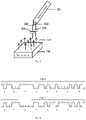
- FIG. 1 shows an application scenario of the method for transmitting a signal according to this embodiment.
- FIG. 1 shows an application scenario of the method for transmitting a signal according to this embodiment.
- a touch screen 104 and an electrode 102 of an active stylus 101 may form a coupling capacitor 103
- the touch screen 104 may use a transmitting (TX)/ receiving (RX) sensor to send a DSSS signal
- the active stylus 101 uses the coupling capacitor 103 to receive the DSSS signal sent by the touch screen 104, and then parses the DSSS signal, so as to implement information interaction between the active stylus 101 and the touch screen 104.
- a flow chart of the method for transmitting a signal according to this embodiment may be as shown in FIG. 2 and include the following steps.
- the DSSS signal sent by the touch screen is received through the coupling capacitor formed between the active stylus and the touch screen.
- the touch screen may perform spread-spectrum coding on a signal to be transmitted to generate the DSSS signal, the touch screen may use the TX/RX sensor to send the DSSS signal, and the active stylus uses the coupling capacitor to receive the DSSS signal sent by the touch screen.
- the coupling capacitor formed between the active stylus and the touch screen may be the coupling capacitor 103 shown in FIG. 1 .
- FIG. 3 also shows a schematic diagram of the coupling capacitor formed between the active stylus and the touch screen.
- the active stylus 101 includes a main electrode 302 and a secondary electrode 303, and the coupling capacitor formed between the active stylus and the touch screen includes: a coupling capacitor 305 formed between the main electrode 302 and the touch screen 104, or a coupling capacitor 306 formed between the secondary electrode 303 and the touch screen 104.
- the active stylus 101 may receive the DSSS signal through the coupling capacitor 305, or may also receive the DSSS signal through the coupling capacitor 306.
- a spread-spectrum coded form of DSSS signals corresponding to "0" and "1" in the USI may be adopted.
- "0” is represented by a 31-bit code 0x58F9A42B
- "1” is represented by a 31-bit code 0x27065BD4
- a duration for which each bit lasts is 1 us.
- This embodiment only takes spread-spectrum coding of DSSS signals in the USI as an example, but is not limited to such type of spread-spectrum coding in the actual application.
- the received DSSS signal is parsed to obtain the signal to be transmitted.
- the DSSS signal received by the active stylus through a coupling capacitor 501 is input to a Comparator Counter DSSS Mixer (CCDM) parsing system 502 in the active stylus, and the CCDM parsing system 502 parses the received DSSS signal to obtain the signal to be transmitted.
- CCDM Comparator Counter DSSS Mixer
- the CCDM parsing system 502 includes: a pre-amplifier circuit 503, a hysteresis comparing circuit 504, and a digital demodulating circuit 505.
- the pre-amplifier circuit 503 pre-amplifies the received DSSS signal, and inputs the pre-amplified DSSS signal into the hysteresis comparing circuit 504.
- the hysteresis comparing circuit 504 restores the pre-amplified DSSS signal to obtain a restored DSSS signal, and inputs the restored DSSS signal into the digital demodulating circuit 505.
- the digital demodulating circuit 505 demodulates the restored DSSS signal, and parses out specific coding information of the DSSS signal, that is, the signal to be transmitted.
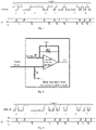
- the pre-amplifier circuit 503 may be an Analog Front End (AFE) circuit, and the AFE circuit may be an inverting amplifier circuit, for example, a low-impedance inverting amplifier circuit shown in FIG. 6 .
- the DSSS signal is used as an input signal of an inverting input end of an operational amplifier (OPA) in the low-impedance inverting amplifier circuit.
- OPA operational amplifier
- a waveform diagram of the input signal and an output signal of the low-impedance inverting amplifier circuit may be as shown in FIG. 7 .
- the input signal is a DSSS signal coded according to the USI, with code 0 as an example, and the output signal is an inverting amplified signal VI.
- VP is a positive output amplitude of the inverting amplified signal
- VN is a negative output amplitude of the inverting amplified signal
- Voltage Common Mode Input (VCMI) is a common mode input voltage
- an output amplitude of the inverting amplified signal may be controlled by configuring parameters of devices such as a resistor and a capacitor in the diagram.
- the AFE circuit may be a non-inverting amplifier circuit, for example, a high-impedance non-inverting amplifier circuit as shown in FIG. 8 .
- the DSSS signal is used as an input signal of a non-inverting input end of an OPA in the high-impedance non-inverting amplifier circuit.
- a waveform diagram of the input signal and an output signal of the high-impedance non-inverting amplifier circuit may be as shown in FIG. 9 .
- the input signal is a DSSS signal coded according to the USI protocol, with code 1 as an example, and the output signal is a non-inverting amplified signal VI, and an output amplitude of the inverting amplified signal may be controlled by configuring parameters of devices such as a resistor and a capacitor in the diagram.
- the hysteresis comparing circuit 504 may be a non-inverting hysteresis comparing circuit or an inverting hysteresis comparing circuit, and the hysteresis comparing circuit 504 will be specifically described below with two examples.
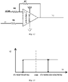
- the hysteresis comparing circuit 504 may be a non-inverting hysteresis comparing circuit in FIG. 10 .
- the non-inverting hysteresis comparing circuit may restore the pre-amplified signal to an original DSSS signal.
- VI as the output signal of the AFE circuit, is used as an input signal of a non-inverting end of a comparator in the hysteresis comparing circuit 504, and V2 is an output signal of the hysteresis comparing circuit.
- a waveform diagram of the input signal and an output signal of the non-inverting hysteresis comparing circuit may be as shown in FIG.
- the hysteresis comparing circuit 504 may also be an inverting hysteresis comparing circuit in FIG. 12 .
- the inverting hysteresis comparing circuit may restore the pre-amplified signal to an inverting signal of the original DSSS signal.
- VI as the output signal of the AFE circuit, is used as an input signal of an inverting end of a comparator in the hysteresis comparing circuit 504.
- the pre-amplifier circuit 503 and the hysteresis comparing circuit 504 may be combined in various modes, for example, the modes of combining the pre-amplifier circuit 503 and the hysteresis comparing circuit 504 may be: combining a high-impedance non-inverting amplifier circuit and a non-inverting hysteresis comparing circuit, combining a high-impedance non-inverting amplifier circuit and an inverting hysteresis comparing circuit, combining a low-impedance inverting amplifier circuit and a non-inverting hysteresis comparing circuit, and combining a low-impedance inverting amplifier circuit and an inverting hysteresis comparing circuit.
- any combination of the pre-amplifier circuit 503 and the hysteresis comparing circuit 504 may restore the original DSSS signal to the non-inverting signal or an inverting signal of the original DSSS signal, for example, if several-bit codes of the original signal are "01101", the restored code is still "01101" for the so-called non-inverting signal, and the restored inverted code is "10010" for the so-called inverting signal.
- the digital demodulating circuit 505 can carry out demodulating the restored signal, and if the restored signal is an inverting signal, the original signal can be obtained only by adding an inverting function to the digital demodulating circuit 505.
- the mode of combining the pre-amplifier circuit 503 and the hysteresis comparing circuit 504 is: combining a low-impedance inverting amplifier circuit 5031 and an inverting hysteresis comparing circuit 5041.
- the DSSS signal received through the coupling capacitor formed between the active stylus and the touch screen is input into an inverting input end of an OPA in the low-impedance inverting amplifier circuit 5031, and an output signal VI of the OPA is input into an inverting input end of the inverting hysteresis comparing circuit 5041.
- FIG. 15 a waveform diagram of an inverting input signal (that is, the DSSS signal) and an output signal VI of the low-impedance inverting amplifier circuit 5031, and an output signal V2 of the inverting hysteresis comparing circuit 5041 is as shown in FIG. 15 , where the DSSS signal takes a DSSS code in the USI protocol as an example, and the DSSS code in FIG. 15 takes a 31-bit code 0x58F9A42B of the code "0" as an example, which, however, is not limited thereto in the actual application. As can be seen from FIG.
- a combination of the low-impedance inverting amplifier circuit 5031 and the inverting hysteresis comparing circuit 5041 may pre-amplify the original DSSS signal and restore the the pre-amplified DSSS signal to a non-inverting signal of the original DSSS signal.
- the mode of combining the pre-amplifier circuit 503 and the hysteresis comparing circuit 504 is: combining a low-impedance inverting amplifier circuit 5032 and a non-inverting hysteresis comparing circuit 5042.
- a DSSS signal is input into an inverting input end of an OPA in the low-impedance inverting amplifier circuit 5032, and an output signal VI of the OPA is input into a non-inverting input end of the non-inverting hysteresis comparing circuit 5042.
- FIG. 17 a waveform diagram of an inverting input signal (that is, the DSSS signal) and the output signal VI of the low-impedance inverting amplifier circuit 5032, and an output signal V2 of the non-inverting hysteresis comparing circuit 5042 is as shown in FIG. 17 , where the DSSS signal takes a DSSS code in the USI protocol as an example, and the DSSS code in FIG. 17 takes a 31-bit code 0x58F9A42B of the code "0" as an example, which, however, is not limited thereto in the actual application. As can be seen from FIG.
- a combination of the low-impedance inverting amplifier circuit 5032 and the non-inverting hysteresis comparing circuit 5042 may pre-amplify the original DSSS signal and restore the pre-amplified DSSS signal to an inverting signal of the original DSSS signal.
- the signal V2 output from the hysteresis comparing circuit 504 is input into the digital demodulating circuit 505, and the digital demodulating circuit 505 demodulates the signal V2 to obtain a signal to be transmitted, thereby implementing information interaction between the touch screen and the active stylus.
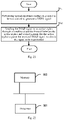
- step 202 may refer to FIG. 18 , which includes the following steps.
- the pre-amplifier circuit pre-amplifies the received DSSS signal.
- the pre-amplified DSSS signal is input into the hysteresis comparing circuit, and the hysteresis comparing circuit restores the pre-amplified DSSS signal to obtain the restored DSSS signal.
- the restored DSSS signal is input into the digital demodulating circuit, and the digital demodulating circuit demodulates the restored DSSS signal and outputs the signal to be transmitted.
- step 601 to step 603 have been described above, and no details will be repeated here.
- the DSSS signal sent by the touch screen is received through the coupling capacitor formed between the active stylus and the touch screen in this embodiment, where the DSSS signal is a spread-spectrum coded signal to be transmitted, and the active stylus parses the received DSSS signal to obtain the signal to be transmitted.
- the DSSS signal is received through capacitive coupling, which can be well applied to DSSS signal transmission in a touch system.
- only one stage of the pre-amplifier circuit, one stage of the hysteresis comparing circuit, and one stage of the digital demodulating circuit are required to perform parsing the received DSSS signal, which renders a simple circuit structure, a small quantity of hardware resources, and relatively low power consumption, and is very applicable to an interactive system of the active stylus and the touch screen that has strict requirements on a circuit size and power consumption, and the like.
- a second embodiment of the present disclosure relates to a method for transmitting a signal.
- This embodiment mainly describes an implementation process of step 603 in the first embodiment in detail, that is to say, specifically describes how to demodulate the restored DSSS signal by the digital demodulating circuit.
- the digital demodulating circuit may adopt a corresponding algorithm to implement a corresponding function thereof.
- FIG. 19 shows a flow chart of a specific algorithm, including the following steps.
- the digital demodulating circuit samples the restored DSSS signal to obtain an original coded signal.
- a restored DSSS signal output by a hysteresis comparing circuit may be sampled at a sampling frequency of N Mhz to obtain an original coded signal 1.
- the original coded signal 1 includes a first type signal, a second type signal and a third type signal, where the first type signal is a spread spectrum code 0x58F9A428 corresponding to "0" in a signal to be transmitted, the second type signal is a spread spectrum code 0x27065BD4 corresponding to "1" in the signal to be transmitted, and the third type signal is an unwanted signal.
- a bitwise XOR operation is performed on the original coded signal and a preset autocorrelation demodulated signal.
- the autocorrelation demodulated signal is shifted as a whole backward by 1 bit, where B is the number of bits of the autocorrelation demodulated signal, that is, the autocorrelation demodulated signal 2 is shifted as a whole on a time axis, so that all the collected B bits of the original coded signal may be subjected to a bitwise XOR operation with the corresponding autocorrelation demodulated signal.
- the autocorrelation demodulated signal may be a first type signal or a second type signal, the autocorrelation demodulated signal takes the first type signal as an example in this embodiment, and as shown in FIG.
- a waveform diagram of the autocorrelation demodulated signal 2 is a waveform diagram of "code 0".
- "0" or "1" is coded with 31-bit data, and a duration at which each bit lasts is 1 us, then the number of points obtained by sampling each bit is N, so the autocorrelation demodulated signal 2 is stored in a 31 ⁇ N wave table.
- the autocorrelation demodulated signal 2 is shifted bitwise, and the above-described bitwise XOR operation performed on the original coded signal 1 and the autocorrelation demodulated signal 2 is repeated.
- a result of the bitwise XOR operation is accumulated to obtain an accumulation result.
- the bitwise XOR result of the collected B bits of the original coded signal and the B-bit autocorrelation demodulated signal are accumulated to obtain the accumulation result.
- an obtained accumulation result is close to 31 ⁇ N.
- an obtained accumulation result is close to 0.
- an XOR operation is performed on the unwanted signal in the original coded signal 1 and the autocorrelation demodulated signal 2
- an obtained accumulation result is close to 31 ⁇ N/2.
- the restored DSSS signal is demodulated according to the accumulation result.
- the restored DSSS signal may be demodulated according to a comparison result between the accumulation result and respective preset thresholds.
- the preset thresholds may include a first preset threshold and a second preset threshold, where the second preset threshold is greater than the first preset threshold.
- the first preset threshold Threshold_L may be a natural number greater than or equal to 0, and less than or equal to B ⁇ N/2, that is, 0 ⁇ Threshold_L ⁇ B ⁇ N/2.
- the second preset threshold Threshold_H may be a natural number greater than B ⁇ N/2, and less than or equal to B ⁇ N, that is, B ⁇ N/2 ⁇ Threshold_H ⁇ B ⁇ N, where B is the number of bits of the autocorrelation demodulated signal. Since the autocorrelation demodulated signal according to this embodiment takes a 31-bit data code as an example, in this embodiment, B is 31, where N is a sampling frequency at which the digital demodulating circuit samples the restored DSSS signal. In other words, in this embodiment, 0 ⁇ Threshold_L ⁇ 31 ⁇ N/2, and 31 ⁇ N/2 ⁇ Threshold_H ⁇ 31 ⁇ N.
- the B bits of the original coded signal is identified as the first type signal. If the accumulation result is detected to be greater than or equal to Threshold_H, then the B bits of the original coded signal is identified as the second type signal. If the accumulation result is detected to be greater than Threshold_L and less than Threshold H, then the B bits of the original coded signal is identified as the unwanted signal.
- Threshold_L and Threshold H the B bits of the original coded signal is identified as the unwanted signal.
- the unwanted signal may be identified.
- the unwanted signals are sampled at moments T0, T1, T2, Tm and Tn, code 1 is sampled when the moment Tm+1 starts, and code 0 is sampled when the moment Tn+1 starts.
- a time at which the collected B bits of the original coded signal starts may also be used as a time at which the identified first type signal starts. If the detected accumulation result is greater than or equal to the second preset threshold, then the time at which the collected B bits of the original coded signal starts may also be used as a time at which the identified second type signal starts.
- a code 1 may be identified, and it can be known that a time at which the code "1" starts is a time at which the collected segment of the original coded signal starts, for example, "an effective signal code 1 starts at the moment Tm+1" marked in the diagram.
- a code 0 may be identified, and it can be known that a time at which the code "0" starts is a time at which the collected segment of the original coded signal starts, for example "an effective signal code 0 starts at the moment Tn+1" marked in the diagram.
- the digital demodulating circuit may demodulate the DSSS signal restored by the hysteresis comparing circuit in this embodiment, detect when the DSSS signal starts, to implement timing synchronization between the touch screen and the active stylus according to the DSSS signal, for better information interaction between the touch screen and the active stylus.
- a third embodiment of the present disclosure which however does not form part of the claimed invention, relates to a method for transmitting a signal, applied to a touch screen.
- a specific flow chart is as shown in FIG. 21 , which includes the following steps.
- spread-spectrum coding is performed on a signal to be transmitted to generate a DSSS signal.
- the DSSS signal is sent to an active stylus through a coupling capacitor formed between the active stylus and a touch screen, for the active stylus to parse the received DSSS signal, to obtain the signal to be transmitted.
- the method for transmitting a signal according to this embodiment is applied to the touch screen
- the method for transmitting a signal according to the first embodiment and the second embodiment are applied to the active stylus, so this embodiment may be implemented in cooperation with the first embodiment and the second embodiment.
- the related technical details as mentioned in the first embodiment and the second embodiment are still valid in this embodiment, and in order to reduce repetition, no details will be repeated here.
- the related technical details as mentioned in this embodiment may also be applied to the first embodiment and the second embodiment.
- the DSSS signal is transmitted through the coupling capacitor formed between the active stylus and the touch screen, which can be well applied to DSSS signal transmission in a touch system in this embodiment.
- only one stage of the pre-amplifier circuit, one stage of the hysteresis comparing circuit, and one stage of the digital demodulating circuit are required to implement parsing the received DSSS signal, which renders a simple circuit structure, a small quantity of hardware resources, and relatively low power consumption, and is very applicable to an interactive system of the active stylus and the touch screen that has strict requirements on a circuit size and power consumption, and the like.
- a fourth embodiment of the present disclosure relates to an active stylus, as shown in FIG. 22 , which includes: at least one processor 901, and a memory 902 connected and in communication with the at least one processor 901, where the memory 902 stores instructions executable by the at least one processor 901, and the instructions, when executed by the at least one processor 901, cause the at least one processor 901 to perform the above-described method for transmitting a signal applied to the active stylus.
- the memory 902 and the processor 901 are connected with each other by means of a bus, the bus may include any number of interconnected buses and bridges, and the bus connects together various circuits of one or more processors and the memory 902.
- the bus may also connect together various other circuits such as peripheral devices, voltage regulators and power management circuits, which are all well known in the art, and thus, will not be described further herein.
- a bus interface provides an interface between the bus and a transceiver.
- the transceiver may be a single element, or may also be a plurality of elements, such as a plurality of receivers and transmitters, which provides a unit for communicating with various other apparatuses over a transmission medium.
- Data processed by the processor 901 is transmitted on a wireless medium through an antenna, and further, the antenna also receives the data from the processor 901 and transmits the data to the processor 901.
- the processor 901 is responsible for managing the bus and general processing, and may further provide various functions, including timing, peripheral interfaces, voltage regulation, power management, and other control functions.
- the memory 902 may be configured to store data used by the processor 901 when the processor 901 executes operations.
- a fifth embodiment of the present disclosure which however does not form part of the claimed invention, relates to a touch screen, as shown in FIG. 23 , including: at least one processor 1001, and a memory 1002 connected and in communication with the at least one processor 1001, where the memory 1002 stores instructions executable by the at least one processor 1001, the instructions, when executed by the at least one processor 1001, causes the at least one processor 1001 to perform the above-described method for transmitting a signal applied to the touch screen.
- the memory 1002 and the processor 1001 are connected with each other by means of a bus, the bus may include any number of interconnected buses and bridges, and the bus connects together various circuits of one or more processors and the memory 1002.
- the bus may also connect together various other circuits such as peripheral devices, voltage regulators and power management circuits, which are all well known in the art, and thus, will not be described further herein.
- a bus interface provides an interface between the bus and a transceiver.
- the transceiver may be a single element, or may also be a plurality of elements, such as a plurality of receivers and transmitters, which provides a unit for communicating with various other apparatuses over a transmission medium.
- Data processed by the processor 1001 is transmitted on a wireless medium through an antenna, and further, the antenna also receives the data from the processor 1001 and transmits the data to the processor 1001.
- the processor 1001 is responsible for managing the bus and general processing, and may further provide various functions, including timing, peripheral interfaces, voltage regulation, power management, and other control functions.
- the memory 1002 may be configured to store data used by the processor 1001 when the processor 1001 executes operations.
- a sixth embodiment of the present disclosure which however does not form part of the claimed invention, relates to a system for transmitting a signal, as shown in FIG. 24 , including: a touch screen 1101 and an active stylus 1102.
- the touch screen 1101 is configured to perform spread-spectrum coding on a signal to be transmitted to generate a DSSS signal.
- the touch screen 1101 is further configured to send the DSSS signal to the active stylus 1102 through a coupling capacitor 1103 formed between the touch screen 1101 and the active stylus 1102.
- the active stylus 1102 is configured to parse the received DSSS signal to obtain the signal to be transmitted.
- this embodiment is a system embodiment corresponding to the first embodiment, the second embodiment and the third embodiment, and this embodiment may be implemented in cooperation with the first embodiment, the second embodiment and the third embodiment.
- the related technical details as mentioned in the first embodiment, the second embodiment and the third embodiment are still valid in this embodiment, and in order to reduce repetition, no details will be repeated here.
- the related technical details as mentioned in this embodiment may also be applied to the first embodiment, the second embodiment and the third embodiment.
- the DSSS signal is transmitted through the coupling capacitor formed between the active stylus and the touch screen in this embodiment, which can be well applied to DSSS signal transmission in a touch system.
- only one stage of the pre-amplifier circuit, one stage of the hysteresis comparing circuit, and one stage of the digital demodulating circuit are required in the active stylus to implement parsing the received DSSS signal, which renders a simple circuit structure, a small quantity of hardware resources, and relatively low power consumption, and is very applicable to the interactive system of the active stylus and the touch screen that has strict requirements on a circuit size and power consumption, and the like.
- a seventh embodiment of the present disclosure relates to a chip, as shown in FIG. 25 , including: a pre-amplifier circuit 1201, configured to pre-amplify a DSSS signal sent by a touch screen and received through a coupling capacitor formed between an active stylus and the touch screen, and output the pre-amplified DSSS signal to a hysteresis comparing circuit 1202; the hysteresis comparing circuit 1202, configured to restore the pre-amplified DSSS signal to obtain the restored DSSS signal and output the restored DSSS signal to a digital demodulating circuit 1203; and the digital demodulating circuit 1203, configured to demodulate the restored DSSS signal.
- a pre-amplifier circuit 1201 configured to pre-amplify a DSSS signal sent by a touch screen and received through a coupling capacitor formed between an active stylus and the touch screen, and output the pre-amplified DSSS signal to a hysteresis comparing circuit 1202
- the pre-amplifier circuit 1201 may include an inverting amplifier circuit or a non-inverting amplifier circuit
- the hysteresis comparing circuit may include: a non-inverting hysteresis comparing circuit or an inverting hysteresis comparing circuit.
- the inverting amplifier circuit may be a low-impedance inverting amplifier circuit as shown in FIG. 6 .
- the low-impedance inverting amplifier circuit includes: a first operational amplifier, a first feedback resistor RF1 and a first feedback capacitor CF1, where the first operational amplifier has a non-inverting input end connected with an input voltage VCMI, and an inverting input end connected with the DSSS signal.
- the first feedback resistor RF1 is bridged between the inverting input end and an output end of the first operational amplifier, and the first feedback capacitor CF1 is connected in parallel with the first feedback resistor RF1.
- the first feedback resistor RF1 has a first end connected with the inverting input end of the first operational amplifier, and a second end connected with the output end of the first operational amplifier.
- the first feedback capacitor CF1 has a first end connected with the first end of the first feedback resistor RF1, and a second end connected with the second end of the first feedback resistor RF1.
- the non-inverting amplifier circuit may be a high-impedance non-inverting amplifier circuit as shown in FIG. 8 .
- the high-impedance non-inverting amplifier circuit includes: a second operational amplifier, a second feedback resistor RF2, a second feedback capacitor CF2, a first resistor R1 and a second resistor R2, where the second operational amplifier has a non-inverting input end connected with the DSSS signal, and an inverting input end connected with a second end of the second resistor R2, and a first end of the second resistor R2 is connected with a first input voltage VCMI1.
- the second feedback resistor RF2 is bridged between the inverting input end and an output end of the second operational amplifier, and the second feedback capacitor CF2 is connected in parallel with the second feedback resistor RF2. That is to say, the second feedback resistor RF2 has a first end connected with the inverting input end of the second operational amplifier, and a second end connected with the output end of the second operational amplifier.
- the second feedback capacitor CF2 has a first end connected with the first end of the second feedback resistor RF2, and a second end connected with the second end of the second feedback resistor RF2.
- the first resistor R1 has a first end connected with the non-inverting input end of the second operational amplifier, and a second end connected with a second input voltage VCMI2, where VCMI1 and VCMI2 may be the same.
- a circuit diagram of the non-inverting hysteresis comparing circuit may be as shown in FIG. 10 , and includes: a first comparator, a third resistor R3, a fourth resistor R4 and a fifth resistor R5.
- the third resistor R3 has a first end connected with an output end VI of the pre-amplifier circuit, and a second end connected with a non-inverting input end of the first comparator.
- the fourth resistor R4 is bridged between the non-inverting input end and an output end of the first comparator. That is to say, the fourth resistor R4 has a first end connected with the second end of the third resistor R3, and a second end connected with an output end V2 of the first comparator.
- the fifth resistor R5 has a first end connected with an input voltage VCMI, and a second end connected with an inverting input end of the first comparator.
- a circuit diagram of the inverting hysteresis comparing circuit may be as shown in FIG. 12 , and includes: a second comparator, a sixth resistor R6, a seventh resistor R7 and an eighth resistor R8, where the sixth resistor R6 has a first end connected with an input voltage VCMI, and a second end connected with a non-inverting input end of the second comparator.
- the seventh resistor R7 is bridged between the non-inverting input end and an output end of the second comparator. That is to say, the seventh resistor R7 has a first end connected with the second end of the sixth resistor R6, and a second end connected with the output end V2 of the second comparator.
- the eighth resistor R8 has a first end connected with the output end VI of the pre-amplifier circuit, and a second end connected with an inverting input end of the second comparator.
- the DSSS signal is transmitted through the coupling capacitor formed between the active stylus and the touch screen in the embodiment of the present disclosure, which can be well applied to DSSS signal transmission in a touch system.
- only one stage of the pre-amplifier circuit, one stage of the hysteresis comparing circuit, and one stage of the digital demodulating circuit are required to implement parsing the received DSSS signal, which renders a simple circuit structure, a small quantity of hardware resources, and relatively low power consumption, and is very applicable to the interactive system of the active stylus and the touch screen that has strict requirements on a circuit size and power consumption, and the like.
- An eighth embodiment of the present disclosure relates to an active stylus, including the chip according to the seventh embodiment.
- a ninth embodiment of the present disclosure relates to a computer-readable storage medium, storing a computer program.
- the computer program when executed by a processor, performs the above-described method for transmitting a signal embodiment.
- the program may be stored in a storage medium, and include a plurality of instructions so that a device (which may be a single chip microcomputer and a chip, and the like) or a processor executes all or some of the steps of the methods as described in the various embodiments of the present disclosure.
- the foregoing storage medium includes: various media that can store program codes, such as a USB flash disk, a mobile hard disk, a Read-Only Memory (ROM), a Random Access Memory (RAM), a magnetic disk or an optical disk.
Landscapes
- Engineering & Computer Science (AREA)
- General Engineering & Computer Science (AREA)
- Theoretical Computer Science (AREA)
- Human Computer Interaction (AREA)
- Physics & Mathematics (AREA)
- General Physics & Mathematics (AREA)
- Position Input By Displaying (AREA)
- Circuits Of Receivers In General (AREA)
Description
- The present disclosure relates to touch technologies, and more particularly, to a method and a system for transmitting a signal, an active stylus, a touch screen and a readable storage medium.
- At present, in a new type of an active stylus touch system, a touch screen may send a direct sequence spread spectrum (DSSS) signal to a stylus end to communicate with the stylus end, so as to perform operations such as synchronizing with the stylus end and sending a command to the stylus end. Thus, how the stylus end correctly receives the DSSS signal sent by the screen end becomes critical.
- In existing technologies, DSSS signal transmission is usually applied in a radio frequency environment, that is, the DSSS signal is transmitted and received through a high-frequency antenna. However, the inventor(s) found that, conditions such as impedance of a screen sensor itself limit spectrum spreading of the DSSS signal, so a mode of transmitting and receiving the DSSS signal through the high-frequency antenna is not applicable to the active stylus touch system that has strict requirements on a structure, a size and power consumption, and the like.
- A patent application
US 20170192534A1 discloses relevant technologies regarding to the active stylus pen, a patent applicationUS 20160226540A1 discloses relevant technologies regarding to a reception circuit, and paper "Implementation and Experimental Demonstration of A Real-time 7-DSSS VLC System Based on FPGA" discloses relevant technologies regarding to using the 7-DSSS technique in VLC system. - The invention is set out in the appended set of claims. The invention as claimed is best understood in light of the embodiments described in the context of
figures 5 and18 together withfigure 2 . Other embodiments mentioned in the description might not disclose the complete combination of features as claimed, but are nevertheless useful for understanding the invention. - One or more embodiments are exemplarily described through the figures in accompanying drawings corresponding thereto, these exemplary descriptions constitute a limitation to the embodiments. In the drawings, elements having the same reference numerals are denoted as similar elements, and unless otherwise stated, the figures in the accompanying drawings do not constitute a limitation of proportion.
-
FIG. 1 is a schematic diagram of an application scenario of a method for transmitting a signal according to a first embodiment of the present disclosure; -
FIG. 2 is a flow chart of the method for transmitting a signal according to the first embodiment of the present disclosure; -
FIG. 3 is a schematic diagram of a coupling capacitor formed between an active stylus and a touch screen according to the first embodiment of the present disclosure; -
FIG. 4 is a waveform diagram of spread spectrum codes of DSSS signals corresponding to "0" and "1" according to the first embodiment of the present disclosure; -
FIG. 5 is a block diagram of implementingstep 202 in the method for transmitting a signal according to the first embodiment of the present disclosure; -
FIG. 6 is a schematic diagram of a low-impedance inverting amplifier circuit according to the first embodiment of the present disclosure; -
FIG. 7 is a waveform diagram of an input signal and an output signal of the low-impedance inverting amplifier circuit according to the first embodiment of the present disclosure; -
FIG. 8 is a schematic diagram of a high-impedance non-inverting amplifier circuit according to the first embodiment of the present disclosure; -
FIG. 9 is a waveform diagram of an input signal and an output signal of the high-impedance non-inverting amplifier circuit according to the first embodiment of the present disclosure; -
FIG. 10 is a schematic diagram of a non-inverting hysteresis comparing circuit according to the first embodiment of the present disclosure; -
FIG. 11 is a waveform diagram of an input signal and an output signal of the non-inverting hysteresis comparing circuit according to the first embodiment of the present disclosure; -
FIG. 12 is a schematic diagram of an inverting hysteresis comparing circuit according to the first embodiment of the present disclosure; -
FIG. 13 is a waveform diagram of an input signal and an output signal of the inverting hysteresis comparing circuit according to the first embodiment of the present disclosure; -
FIG. 14 is a schematic diagram of a circuit combining the low-impedance inverting amplifier circuit and the inverting hysteresis comparing circuit according to the first embodiment of the present disclosure; -
FIG. 15 is a waveform diagram of an input signal and an output signal of a circuit combining the low-impedance inverting amplifier circuit and the inverting hysteresis comparing circuit according to the first embodiment of the present disclosure; -
FIG. 16 is a schematic diagram of a circuit combining the low-impedance inverting amplifier circuit and the non-inverting hysteresis comparing circuit according to the first embodiment of the present disclosure; -
FIG. 17 is a waveform diagram of an input signal and an output signal of a circuit combining the low-impedance inverting amplifier circuit and the non-inverting hysteresis comparing circuit according to the first embodiment of the present disclosure; -
FIG. 18 is a flow chart of an implementation process ofstep 202 according to the first embodiment of the present disclosure; -
FIG. 19 is a flow chart of an implementation process ofstep 603 according to a second embodiment of the present disclosure; -
FIG. 20 is a schematic diagram of identifying an effective signal code by accumulating a result of the bitwise XOR operation on an original codedsignal 1 and an autocorrelation demodulatedsignal 2 according to the second embodiment of the present disclosure; -
FIG. 21 is a flow chart of a method for transmitting a signal according to a third embodiment of the present disclosure; -
FIG. 22 is a structural schematic diagram of an active stylus according to a fourth embodiment of the present disclosure; -
FIG. 23 is a structural schematic diagram of a touch screen according to a fifth embodiment of the present disclosure; -
FIG. 24 is a schematic diagram of a system for transmitting a signal according to a sixth embodiment of the present disclosure; and -
FIG. 25 is a schematic diagram of a chip according to a seventh embodiment of the present disclosure. - In order to make objectives, technical solutions and advantages of the present disclosure more apparent, some embodiments of the present disclosure will be further explained in detail below in combination with accompanying drawings and the embodiments. It should be understood that specific embodiments described herein are merely used for explaining the present disclosure, and not intended to limit the present disclosure.
- A first embodiment of the present disclosure relates to a method for transmitting a signal, applied to products such as a mobile phone, a tablet personal computer and a computer which have an active stylus and a touch function.
FIG. 1 shows an application scenario of the method for transmitting a signal according to this embodiment. InFIG. 1 , atouch screen 104 and anelectrode 102 of anactive stylus 101 may form acoupling capacitor 103, thetouch screen 104 may use a transmitting (TX)/ receiving (RX) sensor to send a DSSS signal, and theactive stylus 101 uses thecoupling capacitor 103 to receive the DSSS signal sent by thetouch screen 104, and then parses the DSSS signal, so as to implement information interaction between theactive stylus 101 and thetouch screen 104. - A flow chart of the method for transmitting a signal according to this embodiment may be as shown in
FIG. 2 and include the following steps. - At
step 201, the DSSS signal sent by the touch screen is received through the coupling capacitor formed between the active stylus and the touch screen. - Specifically, the touch screen may perform spread-spectrum coding on a signal to be transmitted to generate the DSSS signal, the touch screen may use the TX/RX sensor to send the DSSS signal, and the active stylus uses the coupling capacitor to receive the DSSS signal sent by the touch screen. In this embodiment, the coupling capacitor formed between the active stylus and the touch screen may be the
coupling capacitor 103 shown inFIG. 1 . In an actual application,FIG. 3 also shows a schematic diagram of the coupling capacitor formed between the active stylus and the touch screen. As shown inFIG.3 , theactive stylus 101 includes amain electrode 302 and asecondary electrode 303, and the coupling capacitor formed between the active stylus and the touch screen includes: acoupling capacitor 305 formed between themain electrode 302 and thetouch screen 104, or acoupling capacitor 306 formed between thesecondary electrode 303 and thetouch screen 104. Theactive stylus 101 may receive the DSSS signal through thecoupling capacitor 305, or may also receive the DSSS signal through thecoupling capacitor 306. - In addition, in this embodiment, when the spread-spectrum coding is performed on the signal to be transmitted, a spread-spectrum coded form of DSSS signals corresponding to "0" and "1" in the USI may be adopted. As shown in
FIG. 4 , "0" is represented by a 31-bit code 0x58F9A42B, "1" is represented by a 31-bit code 0x27065BD4, and a duration for which each bit lasts is 1 us. This embodiment only takes spread-spectrum coding of DSSS signals in the USI as an example, but is not limited to such type of spread-spectrum coding in the actual application. - At
step 202, the received DSSS signal is parsed to obtain the signal to be transmitted. - Specifically, referring to
FIG. 5 , the DSSS signal received by the active stylus through acoupling capacitor 501 is input to a Comparator Counter DSSS Mixer (CCDM)parsing system 502 in the active stylus, and theCCDM parsing system 502 parses the received DSSS signal to obtain the signal to be transmitted. - The
CCDM parsing system 502 includes: apre-amplifier circuit 503, ahysteresis comparing circuit 504, and adigital demodulating circuit 505. Thepre-amplifier circuit 503 pre-amplifies the received DSSS signal, and inputs the pre-amplified DSSS signal into thehysteresis comparing circuit 504. Thehysteresis comparing circuit 504 restores the pre-amplified DSSS signal to obtain a restored DSSS signal, and inputs the restored DSSS signal into thedigital demodulating circuit 505. Thedigital demodulating circuit 505 demodulates the restored DSSS signal, and parses out specific coding information of the DSSS signal, that is, the signal to be transmitted. - In one example, the
pre-amplifier circuit 503 may be an Analog Front End (AFE) circuit, and the AFE circuit may be an inverting amplifier circuit, for example, a low-impedance inverting amplifier circuit shown inFIG. 6 . The DSSS signal is used as an input signal of an inverting input end of an operational amplifier (OPA) in the low-impedance inverting amplifier circuit. A waveform diagram of the input signal and an output signal of the low-impedance inverting amplifier circuit may be as shown inFIG. 7 . The input signal is a DSSS signal coded according to the USI, withcode 0 as an example, and the output signal is an inverting amplified signal VI. VP is a positive output amplitude of the inverting amplified signal, VN is a negative output amplitude of the inverting amplified signal, Voltage Common Mode Input (VCMI) is a common mode input voltage, and an output amplitude of the inverting amplified signal may be controlled by configuring parameters of devices such as a resistor and a capacitor in the diagram. - In another example, the AFE circuit may be a non-inverting amplifier circuit, for example, a high-impedance non-inverting amplifier circuit as shown in
FIG. 8 . The DSSS signal is used as an input signal of a non-inverting input end of an OPA in the high-impedance non-inverting amplifier circuit. A waveform diagram of the input signal and an output signal of the high-impedance non-inverting amplifier circuit may be as shown inFIG. 9 . The input signal is a DSSS signal coded according to the USI protocol, withcode 1 as an example, and the output signal is a non-inverting amplified signal VI, and an output amplitude of the inverting amplified signal may be controlled by configuring parameters of devices such as a resistor and a capacitor in the diagram. - Further, the
hysteresis comparing circuit 504 may be a non-inverting hysteresis comparing circuit or an inverting hysteresis comparing circuit, and thehysteresis comparing circuit 504 will be specifically described below with two examples. - In one example, the
hysteresis comparing circuit 504 may be a non-inverting hysteresis comparing circuit inFIG. 10 . The non-inverting hysteresis comparing circuit may restore the pre-amplified signal to an original DSSS signal. VI, as the output signal of the AFE circuit, is used as an input signal of a non-inverting end of a comparator in thehysteresis comparing circuit 504, and V2 is an output signal of the hysteresis comparing circuit. A waveform diagram of the input signal and an output signal of the non-inverting hysteresis comparing circuit may be as shown inFIG. 11 , where VTH and VTL are two transition levels, specifically, VTL=VCMI-(VDD-VCMI)∗R3/R4, and VTH=VCMI(1+R3/R4), and VTH and VTL may be adjusted by adjusting magnitudes of R3 and R4. - In another example, the
hysteresis comparing circuit 504 may also be an inverting hysteresis comparing circuit inFIG. 12 . The inverting hysteresis comparing circuit may restore the pre-amplified signal to an inverting signal of the original DSSS signal. VI, as the output signal of the AFE circuit, is used as an input signal of an inverting end of a comparator in thehysteresis comparing circuit 504. A waveform diagram of the input signal and an output signal of the inverting hysteresis comparing circuit may be as shown inFIG. 13 , where VTL=VCMI∗R7/(R7+R6), and VTH=VCMI+(VDD-VCMI)∗R7/R6. - In the actual application, the
pre-amplifier circuit 503 and thehysteresis comparing circuit 504 may be combined in various modes, for example, the modes of combining thepre-amplifier circuit 503 and thehysteresis comparing circuit 504 may be: combining a high-impedance non-inverting amplifier circuit and a non-inverting hysteresis comparing circuit, combining a high-impedance non-inverting amplifier circuit and an inverting hysteresis comparing circuit, combining a low-impedance inverting amplifier circuit and a non-inverting hysteresis comparing circuit, and combining a low-impedance inverting amplifier circuit and an inverting hysteresis comparing circuit. Any combination of thepre-amplifier circuit 503 and thehysteresis comparing circuit 504 may restore the original DSSS signal to the non-inverting signal or an inverting signal of the original DSSS signal, for example, if several-bit codes of the original signal are "01101", the restored code is still "01101" for the so-called non-inverting signal, and the restored inverted code is "10010" for the so-called inverting signal. Regardless of whether a non-inverting signal or an inverting signal is restored, thedigital demodulating circuit 505 can carry out demodulating the restored signal, and if the restored signal is an inverting signal, the original signal can be obtained only by adding an inverting function to thedigital demodulating circuit 505. - In one example, the mode of combining the
pre-amplifier circuit 503 and thehysteresis comparing circuit 504 is: combining a low-impedanceinverting amplifier circuit 5031 and an invertinghysteresis comparing circuit 5041. Referring toFIG. 14 , the DSSS signal received through the coupling capacitor formed between the active stylus and the touch screen is input into an inverting input end of an OPA in the low-impedanceinverting amplifier circuit 5031, and an output signal VI of the OPA is input into an inverting input end of the invertinghysteresis comparing circuit 5041. Further, a waveform diagram of an inverting input signal (that is, the DSSS signal) and an output signal VI of the low-impedanceinverting amplifier circuit 5031, and an output signal V2 of the invertinghysteresis comparing circuit 5041 is as shown inFIG. 15 , where the DSSS signal takes a DSSS code in the USI protocol as an example, and the DSSS code inFIG. 15 takes a 31-bit code 0x58F9A42B of the code "0" as an example, which, however, is not limited thereto in the actual application. As can be seen fromFIG. 15 , a combination of the low-impedanceinverting amplifier circuit 5031 and the invertinghysteresis comparing circuit 5041 may pre-amplify the original DSSS signal and restore the the pre-amplified DSSS signal to a non-inverting signal of the original DSSS signal. - In another example, the mode of combining the
pre-amplifier circuit 503 and thehysteresis comparing circuit 504 is: combining a low-impedanceinverting amplifier circuit 5032 and a non-invertinghysteresis comparing circuit 5042. Referring toFIG. 16 , a DSSS signal is input into an inverting input end of an OPA in the low-impedanceinverting amplifier circuit 5032, and an output signal VI of the OPA is input into a non-inverting input end of the non-invertinghysteresis comparing circuit 5042. Further, a waveform diagram of an inverting input signal (that is, the DSSS signal) and the output signal VI of the low-impedanceinverting amplifier circuit 5032, and an output signal V2 of the non-invertinghysteresis comparing circuit 5042 is as shown inFIG. 17 , where the DSSS signal takes a DSSS code in the USI protocol as an example, and the DSSS code inFIG. 17 takes a 31-bit code 0x58F9A42B of the code "0" as an example, which, however, is not limited thereto in the actual application. As can be seen fromFIG. 17 , a combination of the low-impedanceinverting amplifier circuit 5032 and the non-invertinghysteresis comparing circuit 5042 may pre-amplify the original DSSS signal and restore the pre-amplified DSSS signal to an inverting signal of the original DSSS signal. - Finally, the signal V2 output from the
hysteresis comparing circuit 504 is input into thedigital demodulating circuit 505, and thedigital demodulating circuit 505 demodulates the signal V2 to obtain a signal to be transmitted, thereby implementing information interaction between the touch screen and the active stylus. - To further facilitate understanding, an implementation process of
step 202 may refer toFIG. 18 , which includes the following steps. - At
step 601, the pre-amplifier circuit pre-amplifies the received DSSS signal. - At
step 602, the pre-amplified DSSS signal is input into the hysteresis comparing circuit, and the hysteresis comparing circuit restores the pre-amplified DSSS signal to obtain the restored DSSS signal. - At
step 603, the restored DSSS signal is input into the digital demodulating circuit, and the digital demodulating circuit demodulates the restored DSSS signal and outputs the signal to be transmitted. - The above-described
step 601 to step 603 have been described above, and no details will be repeated here. - Compared with existing technologies, the DSSS signal sent by the touch screen is received through the coupling capacitor formed between the active stylus and the touch screen in this embodiment, where the DSSS signal is a spread-spectrum coded signal to be transmitted, and the active stylus parses the received DSSS signal to obtain the signal to be transmitted. The DSSS signal is received through capacitive coupling, which can be well applied to DSSS signal transmission in a touch system. In addition, in this embodiment, only one stage of the pre-amplifier circuit, one stage of the hysteresis comparing circuit, and one stage of the digital demodulating circuit are required to perform parsing the received DSSS signal, which renders a simple circuit structure, a small quantity of hardware resources, and relatively low power consumption, and is very applicable to an interactive system of the active stylus and the touch screen that has strict requirements on a circuit size and power consumption, and the like.
- A second embodiment of the present disclosure relates to a method for transmitting a signal. This embodiment mainly describes an implementation process of
step 603 in the first embodiment in detail, that is to say, specifically describes how to demodulate the restored DSSS signal by the digital demodulating circuit. The digital demodulating circuit may adopt a corresponding algorithm to implement a corresponding function thereof. Please refer toFIG. 19 , which shows a flow chart of a specific algorithm, including the following steps. - At
step 701, the digital demodulating circuit samples the restored DSSS signal to obtain an original coded signal. - In this embodiment, the USI is taken as an example for description, specifically, a restored DSSS signal output by a hysteresis comparing circuit may be sampled at a sampling frequency of N Mhz to obtain an original
coded signal 1. The originalcoded signal 1 includes a first type signal, a second type signal and a third type signal, where the first type signal is a spread spectrum code 0x58F9A428 corresponding to "0" in a signal to be transmitted, the second type signal is a spread spectrum code 0x27065BD4 corresponding to "1" in the signal to be transmitted, and the third type signal is an unwanted signal. - At
step 702, a bitwise XOR operation is performed on the original coded signal and a preset autocorrelation demodulated signal. - Specifically, after every B bits of the original coded signal are collected, the autocorrelation demodulated signal is shifted as a whole backward by 1 bit, where B is the number of bits of the autocorrelation demodulated signal, that is, the autocorrelation demodulated
signal 2 is shifted as a whole on a time axis, so that all the collected B bits of the original coded signal may be subjected to a bitwise XOR operation with the corresponding autocorrelation demodulated signal. The autocorrelation demodulated signal may be a first type signal or a second type signal, the autocorrelation demodulated signal takes the first type signal as an example in this embodiment, and as shown inFIG. 20 , a waveform diagram of the autocorrelation demodulatedsignal 2 is a waveform diagram of "code 0". According to characteristics of the DSSS signals in the USI protocol, "0" or "1" is coded with 31-bit data, and a duration at which each bit lasts is 1 us, then the number of points obtained by sampling each bit is N, so the autocorrelation demodulatedsignal 2 is stored in a 31∗N wave table. As each sampling point is collected, the autocorrelation demodulatedsignal 2 is shifted bitwise, and the above-described bitwise XOR operation performed on the originalcoded signal 1 and the autocorrelation demodulatedsignal 2 is repeated. - At
step 703, a result of the bitwise XOR operation is accumulated to obtain an accumulation result. - Specifically, the bitwise XOR result of the collected B bits of the original coded signal and the B-bit autocorrelation demodulated signal are accumulated to obtain the accumulation result. Usually, when a synchronous XOR operation is performed on a segment of code "1" in
signal 1 and an autocorrelation demodulatedsignal 2, an obtained accumulation result is close to 31∗N. When a synchronous XOR operation is performed on a segment of code "0" in the originalcoded signal 1 and the autocorrelation demodulatedsignal 2, an obtained accumulation result is close to 0. When an XOR operation is performed on the unwanted signal in the originalcoded signal 1 and the autocorrelation demodulatedsignal 2, an obtained accumulation result is close to 31∗N/2. - At
step 704, the restored DSSS signal is demodulated according to the accumulation result. - Specifically, the restored DSSS signal may be demodulated according to a comparison result between the accumulation result and respective preset thresholds. The preset thresholds may include a first preset threshold and a second preset threshold, where the second preset threshold is greater than the first preset threshold. In the actual application, the first preset threshold Threshold_L may be a natural number greater than or equal to 0, and less than or equal to B∗N/2, that is, 0≤Threshold_L≤B∗N/2. The second preset threshold Threshold_H may be a natural number greater than B∗N/2, and less than or equal to B∗N, that is, B∗N/2<Threshold_H≤B∗N, where B is the number of bits of the autocorrelation demodulated signal. Since the autocorrelation demodulated signal according to this embodiment takes a 31-bit data code as an example, in this embodiment, B is 31, where N is a sampling frequency at which the digital demodulating circuit samples the restored DSSS signal. In other words, in this embodiment, 0≤Threshold_L≤31∗N/2, and 31∗N/2<Threshold_H≤31∗N.
- Further, if the accumulation result is detected to be less than or equal to Threshold_L, then the B bits of the original coded signal is identified as the first type signal. If the accumulation result is detected to be greater than or equal to Threshold_H, then the B bits of the original coded signal is identified as the second type signal. If the accumulation result is detected to be greater than Threshold_L and less than Threshold H, then the B bits of the original coded signal is identified as the unwanted signal. To facilitate understanding, please refer to
FIG. 20 , if the accumulation result is greater than Threshold H,code 1 may be identified, if the accumulation result is less than Threshold L,code 0 may be identified, and if the accumulation result is less than Threshold_H and greater than Threshold L, the unwanted signal may be identified. As can be seen fromFIG. 20 , the unwanted signals are sampled at moments T0, T1, T2, Tm and Tn,code 1 is sampled when the moment Tm+1 starts, andcode 0 is sampled when the moment Tn+1 starts. - In the actual application, if the accumulation result is detected to be less than or equal to the first preset threshold, then a time at which the collected B bits of the original coded signal starts may also be used as a time at which the identified first type signal starts. If the detected accumulation result is greater than or equal to the second preset threshold, then the time at which the collected B bits of the original coded signal starts may also be used as a time at which the identified second type signal starts. To facilitate understanding, please refer to
FIG. 20 , if the accumulation result is greater than Threshold_H, acode 1 may be identified, and it can be known that a time at which the code "1" starts is a time at which the collected segment of the original coded signal starts, for example, "aneffective signal code 1 starts at the moment Tm+1" marked in the diagram. If the accumulation result is less than Threshold_L, acode 0 may be identified, and it can be known that a time at which the code "0" starts is a time at which the collected segment of the original coded signal starts, for example "aneffective signal code 0 starts at the moment Tn+1" marked in the diagram. - Compared with existing technologies, the digital demodulating circuit may demodulate the DSSS signal restored by the hysteresis comparing circuit in this embodiment, detect when the DSSS signal starts, to implement timing synchronization between the touch screen and the active stylus according to the DSSS signal, for better information interaction between the touch screen and the active stylus.
- A third embodiment of the present disclosure, which however does not form part of the claimed invention, relates to a method for transmitting a signal, applied to a touch screen. A specific flow chart is as shown in
FIG. 21 , which includes the following steps. - At
step 801, spread-spectrum coding is performed on a signal to be transmitted to generate a DSSS signal. - At
step 802, the DSSS signal is sent to an active stylus through a coupling capacitor formed between the active stylus and a touch screen, for the active stylus to parse the received DSSS signal, to obtain the signal to be transmitted. - It is not difficult to find that, the method for transmitting a signal according to this embodiment is applied to the touch screen, the method for transmitting a signal according to the first embodiment and the second embodiment are applied to the active stylus, so this embodiment may be implemented in cooperation with the first embodiment and the second embodiment. The related technical details as mentioned in the first embodiment and the second embodiment are still valid in this embodiment, and in order to reduce repetition, no details will be repeated here. Correspondingly, the related technical details as mentioned in this embodiment may also be applied to the first embodiment and the second embodiment.
- Compared with existing technologies, the DSSS signal is transmitted through the coupling capacitor formed between the active stylus and the touch screen, which can be well applied to DSSS signal transmission in a touch system in this embodiment. In addition, in this embodiment, only one stage of the pre-amplifier circuit, one stage of the hysteresis comparing circuit, and one stage of the digital demodulating circuit are required to implement parsing the received DSSS signal, which renders a simple circuit structure, a small quantity of hardware resources, and relatively low power consumption, and is very applicable to an interactive system of the active stylus and the touch screen that has strict requirements on a circuit size and power consumption, and the like.
- The steps of the above various methods are divided only for clarity of description, the steps, when performed, may be merged into one step or some steps may be split into a plurality of steps, which are all within the protection scope of this patent as long as they include the same logical relationship. Additions of insignificant modifications or introductions of insignificant design to algorithms or processes without changing a core design of the algorithms and processes, are all within the protection scope of this patent.
- A fourth embodiment of the present disclosure relates to an active stylus, as shown in
FIG. 22 , which includes: at least oneprocessor 901, and amemory 902 connected and in communication with the at least oneprocessor 901, where thememory 902 stores instructions executable by the at least oneprocessor 901, and the instructions, when executed by the at least oneprocessor 901, cause the at least oneprocessor 901 to perform the above-described method for transmitting a signal applied to the active stylus. - The
memory 902 and theprocessor 901 are connected with each other by means of a bus, the bus may include any number of interconnected buses and bridges, and the bus connects together various circuits of one or more processors and thememory 902. The bus may also connect together various other circuits such as peripheral devices, voltage regulators and power management circuits, which are all well known in the art, and thus, will not be described further herein. A bus interface provides an interface between the bus and a transceiver. The transceiver may be a single element, or may also be a plurality of elements, such as a plurality of receivers and transmitters, which provides a unit for communicating with various other apparatuses over a transmission medium. Data processed by theprocessor 901 is transmitted on a wireless medium through an antenna, and further, the antenna also receives the data from theprocessor 901 and transmits the data to theprocessor 901. - The
processor 901 is responsible for managing the bus and general processing, and may further provide various functions, including timing, peripheral interfaces, voltage regulation, power management, and other control functions. Thememory 902 may be configured to store data used by theprocessor 901 when theprocessor 901 executes operations. - A fifth embodiment of the present disclosure, which however does not form part of the claimed invention, relates to a touch screen, as shown in
FIG. 23 , including: at least oneprocessor 1001, and amemory 1002 connected and in communication with the at least oneprocessor 1001, where thememory 1002 stores instructions executable by the at least oneprocessor 1001, the instructions, when executed by the at least oneprocessor 1001, causes the at least oneprocessor 1001 to perform the above-described method for transmitting a signal applied to the touch screen. - The
memory 1002 and theprocessor 1001 are connected with each other by means of a bus, the bus may include any number of interconnected buses and bridges, and the bus connects together various circuits of one or more processors and thememory 1002. The bus may also connect together various other circuits such as peripheral devices, voltage regulators and power management circuits, which are all well known in the art, and thus, will not be described further herein. A bus interface provides an interface between the bus and a transceiver. The transceiver may be a single element, or may also be a plurality of elements, such as a plurality of receivers and transmitters, which provides a unit for communicating with various other apparatuses over a transmission medium. Data processed by theprocessor 1001 is transmitted on a wireless medium through an antenna, and further, the antenna also receives the data from theprocessor 1001 and transmits the data to theprocessor 1001. - The
processor 1001 is responsible for managing the bus and general processing, and may further provide various functions, including timing, peripheral interfaces, voltage regulation, power management, and other control functions. Thememory 1002 may be configured to store data used by theprocessor 1001 when theprocessor 1001 executes operations. - A sixth embodiment of the present disclosure, which however does not form part of the claimed invention, relates to a system for transmitting a signal, as shown in
FIG. 24 , including: atouch screen 1101 and anactive stylus 1102. Thetouch screen 1101 is configured to perform spread-spectrum coding on a signal to be transmitted to generate a DSSS signal. Thetouch screen 1101 is further configured to send the DSSS signal to theactive stylus 1102 through acoupling capacitor 1103 formed between thetouch screen 1101 and theactive stylus 1102. Theactive stylus 1102 is configured to parse the received DSSS signal to obtain the signal to be transmitted. - It is not difficult to find that, this embodiment is a system embodiment corresponding to the first embodiment, the second embodiment and the third embodiment, and this embodiment may be implemented in cooperation with the first embodiment, the second embodiment and the third embodiment. The related technical details as mentioned in the first embodiment, the second embodiment and the third embodiment are still valid in this embodiment, and in order to reduce repetition, no details will be repeated here. Correspondingly, the related technical details as mentioned in this embodiment may also be applied to the first embodiment, the second embodiment and the third embodiment.
- Compared with existing technologies, the DSSS signal is transmitted through the coupling capacitor formed between the active stylus and the touch screen in this embodiment, which can be well applied to DSSS signal transmission in a touch system. In addition, in this embodiment, only one stage of the pre-amplifier circuit, one stage of the hysteresis comparing circuit, and one stage of the digital demodulating circuit are required in the active stylus to implement parsing the received DSSS signal, which renders a simple circuit structure, a small quantity of hardware resources, and relatively low power consumption, and is very applicable to the interactive system of the active stylus and the touch screen that has strict requirements on a circuit size and power consumption, and the like.
- A seventh embodiment of the present disclosure relates to a chip, as shown in
FIG. 25 , including: apre-amplifier circuit 1201, configured to pre-amplify a DSSS signal sent by a touch screen and received through a coupling capacitor formed between an active stylus and the touch screen, and output the pre-amplified DSSS signal to ahysteresis comparing circuit 1202; thehysteresis comparing circuit 1202, configured to restore the pre-amplified DSSS signal to obtain the restored DSSS signal and output the restored DSSS signal to adigital demodulating circuit 1203; and thedigital demodulating circuit 1203, configured to demodulate the restored DSSS signal. - In one example, the
pre-amplifier circuit 1201 may include an inverting amplifier circuit or a non-inverting amplifier circuit, and the hysteresis comparing circuit may include: a non-inverting hysteresis comparing circuit or an inverting hysteresis comparing circuit. - In one example, the inverting amplifier circuit may be a low-impedance inverting amplifier circuit as shown in
FIG. 6 . The low-impedance inverting amplifier circuit includes: a first operational amplifier, a first feedback resistor RF1 and a first feedback capacitor CF1, where the first operational amplifier has a non-inverting input end connected with an input voltage VCMI, and an inverting input end connected with the DSSS signal. The first feedback resistor RF1 is bridged between the inverting input end and an output end of the first operational amplifier, and the first feedback capacitor CF1 is connected in parallel with the first feedback resistor RF1. That is to say, the first feedback resistor RF1 has a first end connected with the inverting input end of the first operational amplifier, and a second end connected with the output end of the first operational amplifier. The first feedback capacitor CF1 has a first end connected with the first end of the first feedback resistor RF1, and a second end connected with the second end of the first feedback resistor RF1. - In one example, the non-inverting amplifier circuit may be a high-impedance non-inverting amplifier circuit as shown in
FIG. 8 . The high-impedance non-inverting amplifier circuit includes: a second operational amplifier, a second feedback resistor RF2, a second feedback capacitor CF2, a first resistor R1 and a second resistor R2, where the second operational amplifier has a non-inverting input end connected with the DSSS signal, and an inverting input end connected with a second end of the second resistor R2, and a first end of the second resistor R2 is connected with a first input voltage VCMI1. The second feedback resistor RF2 is bridged between the inverting input end and an output end of the second operational amplifier, and the second feedback capacitor CF2 is connected in parallel with the second feedback resistor RF2. That is to say, the second feedback resistor RF2 has a first end connected with the inverting input end of the second operational amplifier, and a second end connected with the output end of the second operational amplifier. The second feedback capacitor CF2 has a first end connected with the first end of the second feedback resistor RF2, and a second end connected with the second end of the second feedback resistor RF2. The first resistor R1 has a first end connected with the non-inverting input end of the second operational amplifier, and a second end connected with a second input voltage VCMI2, where VCMI1 and VCMI2 may be the same. - In one example, a circuit diagram of the non-inverting hysteresis comparing circuit may be as shown in
FIG. 10 , and includes: a first comparator, a third resistor R3, a fourth resistor R4 and a fifth resistor R5. The third resistor R3 has a first end connected with an output end VI of the pre-amplifier circuit, and a second end connected with a non-inverting input end of the first comparator. The fourth resistor R4 is bridged between the non-inverting input end and an output end of the first comparator. That is to say, the fourth resistor R4 has a first end connected with the second end of the third resistor R3, and a second end connected with an output end V2 of the first comparator. The fifth resistor R5 has a first end connected with an input voltage VCMI, and a second end connected with an inverting input end of the first comparator. - In one example, a circuit diagram of the inverting hysteresis comparing circuit may be as shown in
FIG. 12 , and includes: a second comparator, a sixth resistor R6, a seventh resistor R7 and an eighth resistor R8, where the sixth resistor R6 has a first end connected with an input voltage VCMI, and a second end connected with a non-inverting input end of the second comparator. The seventh resistor R7 is bridged between the non-inverting input end and an output end of the second comparator. That is to say, the seventh resistor R7 has a first end connected with the second end of the sixth resistor R6, and a second end connected with the output end V2 of the second comparator. The eighth resistor R8 has a first end connected with the output end VI of the pre-amplifier circuit, and a second end connected with an inverting input end of the second comparator. - Compared with existing technologies, the DSSS signal is transmitted through the coupling capacitor formed between the active stylus and the touch screen in the embodiment of the present disclosure, which can be well applied to DSSS signal transmission in a touch system. In addition, in this embodiment, only one stage of the pre-amplifier circuit, one stage of the hysteresis comparing circuit, and one stage of the digital demodulating circuit are required to implement parsing the received DSSS signal, which renders a simple circuit structure, a small quantity of hardware resources, and relatively low power consumption, and is very applicable to the interactive system of the active stylus and the touch screen that has strict requirements on a circuit size and power consumption, and the like.
- An eighth embodiment of the present disclosure relates to an active stylus, including the chip according to the seventh embodiment.
- A ninth embodiment of the present disclosure relates to a computer-readable storage medium, storing a computer program. The computer program, when executed by a processor, performs the above-described method for transmitting a signal embodiment.
- That is, those skilled in the art may understand that implementation of all or some of the steps in the methods according to the above-described embodiments may be completed by related hardware as instructed by a program, the program may be stored in a storage medium, and include a plurality of instructions so that a device (which may be a single chip microcomputer and a chip, and the like) or a processor executes all or some of the steps of the methods as described in the various embodiments of the present disclosure. The foregoing storage medium includes: various media that can store program codes, such as a USB flash disk, a mobile hard disk, a Read-Only Memory (ROM), a Random Access Memory (RAM), a magnetic disk or an optical disk.
Claims (15)
- A method for signal transfer, applied by an active stylus (101), and comprising:receiving (201), by an electrode (102, 302, 303) in the active stylus (101), a direct sequence spread spectrum, DSSS, signal, wherein the DSSS signal is sent by a touch screen (104) via a coupling capacitor (103, 305, 306, 501) formed between the electrode (102, 302, 303) and the touch screen (104)pre-amplifying (601), by a pre-amplifier circuit (503) in the active stylus (101), the received DSSS signal;inputting (602), by the pre-amplifier circuit (503), the pre-amplified DSSS signal into a hysteresis comparing circuit (504), the hysteresis comparing circuit (504) being a comparator circuit with hysteresis;restoring (602), by the hysteresis comparing circuit (504), the pre-amplified DSSS signal to obtain a restored DSSS signal according to the originally sent DSSS signal;inputting (603), by the hysteresis comparing circuit (504), the restored DSSS signal to a digital demodulating circuit (505);demodulating (603), by the digital demodulating circuit (505), the restored DSSS signal to obtain an original signal that is not spread-spectrum coded; and outputting (603), by the digital demodulating circuit (505), the original signal.
- The method for signal transfer according to claim 1, wherein demodulating, by the digital demodulating circuit (505), the restored DSSS signal comprises:sampling (701), by the digital demodulating circuit (505), the restored DSSS signal to obtain an original coded signal;performing (702) a bitwise XOR operation on the original coded signal and a preset autocorrelation demodulated signal;accumulating (703) a result of the bitwise XOR operation to obtain an accumulation result; anddemodulating (704) the restored DSSS signal according to the accumulation result.
- The method for signal transfer according to claim 2, wherein performing the bitwise XOR operation on the original coded signal and the preset autocorrelation demodulated signal comprises:shifting the autocorrelation demodulated signal as a whole backward by 1 bit after every B bits of the original coded signal are collected, where B is the number of bits of the autocorrelation demodulated signal; wherein each bit includes N sampling points, and the shifting is repeated as each sampling point is collected;performing the bitwise XOR operation on the collected B bits of the original coded signal and the B-bit autocorrelation demodulated signal;accumulating the result of the bitwise XOR operation of the collected B bits of the original coded signal and the B-bit autocorrelation demodulated signal to obtain the accumulation result;demodulating the restored DSSS signal according to a comparison result between the accumulation result and a preset threshold.
- The method for signal transfer according to claim 3, wherein the original coded signal comprises a first type signal, a second type signal and a third type signal, wherein the first type signal is a spread spectrum code corresponding to "0" in the original signal, the second type signal is a spread spectrum code corresponding to "1" in the original signal, and the third type signal is an unwanted signal;if the accumulation result is detected to be less than or equal to a first preset threshold, identifying the collected B bits of the original coded signal as the first type signal;if the accumulation result is detected to be greater than or equal to a second preset threshold, identifying the collected B bits of the original coded signal as the second type signal, wherein the second preset threshold is greater than the first preset threshold;if the accumulation result is detected to be greater than the first preset threshold and less than the second preset threshold, identifying the collected B bits of the original coded signal as the unwanted signal.
- The method for signal transfer according to claim 4, wherein if the accumulation result is detected to be less than or equal to the first preset threshold, the method further comprises: using a time at which the collected B bits of the original coded signal starts as a time at which the identified first type signal starts;
if the accumulation result is detected to be greater than or equal to the second preset threshold, the method further comprises: using a time at which the collected B bits of the original coded signal starts as a time at which the identified second type signal starts. - The method for signal transfer according to claim 4, wherein the first preset threshold is greater than or equal to 0, and less than or equal to B∗N/2, the second preset threshold is greater than B∗N/2, and less than or equal to B∗N, wherein N is a sampling frequency at which the digital demodulating circuit samples the restored DSSS signal.
- The method for signal transfer according to any one of claims 1-6, wherein the pre-amplifier circuit comprises: a non-inverting amplifier circuit or an inverting amplifier circuit (5031, 5032).
- The method for signal transfer according to any one of claims 1-7, wherein the hysteresis comparing circuit comprises: a non-inverting hysteresis comparing circuit or an inverting hysteresis comparing circuit (5041, 5042).
- The method for signal transfer according to any one of claims 1 to 8, wherein the active stylus comprises a main electrode and a secondary electrode, and the coupling capacitor formed between the active stylus and the touch screen comprises:
a coupling capacitor formed between the main electrode and the touch screen, or a coupling capacitor formed between the secondary electrode and the touch screen. - A chip, comprising a pre-amplifier circuit (503), a hysteresis comparing circuit and a digital demodulating circuit (505);wherein the pre-amplifier circuit (503) is configured to pre-amplify a direct sequence spread spectrum, DSSS, signal sent by a touch screen (104) via a coupling capacitor (103, 305, 306, 501) formed between an electrode (102, 302, 303) in an active stylus (101) and the touch screen (104), wherein the DSSS signal is pre-amplified when it is received by the active stylus (101), and the pre-amplifier circuit (503) is further configured to output the pre-amplified DSSS signal to the hysteresis comparing circuit (504), wherein the hysteresis comparing circuit (504) is a comparator circuit with hysteresis;the hysteresis comparing circuit (504) is configured to restore the pre-amplified DSSS signal to obtain a restored DSSS signal according to the originally sent DSSS signal, and output the restored DSSS signal to the digital demodulating circuit (505);the digital demodulating circuit (505) is configured to demodulate the restored DSSS signal to obtain an original signal that is not spread-spectrum coded, and output the original signal.
- The chip according to claim 10, wherein the digital demodulating circuit (505) is configured to:sample, by the digital demodulating circuit (505), the restored DSSS signal to obtain an original coded signal;perform a bitwise XOR operation on the original coded signal and a preset autocorrelation demodulated signal;accumulate a result of the bitwise XOR operation to obtain an accumulation result; anddemodulate the restored DSSS signal according to the accumulation result.
- The chip according to claim 11, wherein the digital demodulating circuit (505) is configured to:shift the autocorrelation demodulated signal as a whole backward by 1 bit after every B bits of the original coded signal are collected, where B is the number of bits of the autocorrelation demodulated signal; wherein each bit includes N sampling points, and the shifting is repeated as each sampling point is collected;perform the bitwise XOR operation on the collected B bits of the original coded signal and the B-bit autocorrelation demodulated signal;accumulate the result of the bitwise XOR operation of the collected B bits of the original coded signal and the B-bit autocorrelation demodulated signal to obtain the accumulation result;demodulate the restored DSSS signal according to a comparison result between the accumulation result and a preset threshold.
- The chip according to any one of claims 10-12, wherein the pre-amplifier circuit comprises: an inverting amplifier circuit (5031, 5032) or a non-inverting amplifier circuit;wherein the inverting amplifier circuit (5031, 5032) comprises a low-impedance inverting amplifier circuit, and the low-impedance inverting amplifier circuit comprises: a first operational amplifier, a first feedback resistor and a first feedback capacitor, wherein the first operational amplifier has a non-inverting input end connected with an input voltage, and an inverting input end connected with the DSSS signal; the first feedback resistor is bridged between the inverting input end and an output end of the first operational amplifier, and the first feedback capacitor is connected in parallel with the first feedback resistor; orwherein the non-inverting amplifier circuit comprises a high-impedance non-inverting amplifier circuit, and the high-impedance non-inverting amplifier circuit comprises: a second operational amplifier, a second feedback resistor, a second feedback capacitor, a first resistor and a second resistor, the second operational amplifier has a non-inverting input end connected with the DSSS signal, an inverting input end connected with a second end of the second resistor, and a first end of the second resistor is connected with a first input voltage; the second feedback resistor is bridged between the inverting input end and an output end of the second operational amplifier; the second feedback capacitor is connected in parallel with the second feedback resistor, and the first resistor has a first end connected with the non-inverting input end of the second operational amplifier, and a second end connected with a second input voltage.
- The chip according to any one of claims 10-13, wherein the hysteresis comparing circuit comprises a non-inverting hysteresis comparing circuit or an inverting hysteresis comparing circuit (5041, 5042);the non-inverting hysteresis comparing circuit comprises: a first comparator, a third resistor, a fourth resistor and a fifth resistor, the third resistor has a first end connected with an output end of the pre-amplifier circuit, and a second end connected with a non-inverting input end of the first comparator, the fourth resistor is bridged between the non-inverting input end and an output end of the first comparator, and the fifth resistor has a first end connected with an input voltage, and a second end connected with an inverting input end of the first comparator; orthe inverting hysteresis comparing circuit (5041, 5042) comprises: a second comparator, a sixth resistor, a seventh resistor and an eighth resistor; wherein the sixth resistor has a first end connected with an input voltage, and a second end connected with a non-inverting input end of the second comparator, the seventh resistor is bridged between the non-inverting input end and an output end of the second comparator, the eighth resistor has a first end connected with the output end of the pre-amplifier circuit, and a second end connected with an inverting input end of the second comparator.
- An active stylus, comprising:
the chip according to any one of claims 10 to 14.
Applications Claiming Priority (1)
| Application Number | Priority Date | Filing Date | Title |
|---|---|---|---|
| PCT/CN2019/079550 WO2020191585A1 (en) | 2019-03-25 | 2019-03-25 | Signal transmission method and system, active stylus, touch screen, and readable storage medium |
Publications (3)
| Publication Number | Publication Date |
|---|---|
| EP3764203A1 EP3764203A1 (en) | 2021-01-13 |
| EP3764203A4 EP3764203A4 (en) | 2021-05-12 |
| EP3764203B1 true EP3764203B1 (en) | 2022-11-16 |
Family
ID=72608748
Family Applications (1)
| Application Number | Title | Priority Date | Filing Date |
|---|---|---|---|
| EP19920633.5A Active EP3764203B1 (en) | 2019-03-25 | 2019-03-25 | Signal transmission method and system, active stylus, touch screen, and readable storage medium |
Country Status (4)
| Country | Link |
|---|---|
| US (1) | US11106318B2 (en) |
| EP (1) | EP3764203B1 (en) |
| CN (1) | CN112074803A (en) |
| WO (1) | WO2020191585A1 (en) |
Families Citing this family (2)
| Publication number | Priority date | Publication date | Assignee | Title |
|---|---|---|---|---|
| WO2022165839A1 (en) * | 2021-02-08 | 2022-08-11 | 深圳市汇顶科技股份有限公司 | Method for preventing interference, touch chip, and active pen chip |
| CN116048289B (en) * | 2022-08-25 | 2024-08-06 | 荣耀终端有限公司 | Water outlet control method of handwriting pen and electronic equipment |
Family Cites Families (10)
| Publication number | Priority date | Publication date | Assignee | Title |
|---|---|---|---|---|
| CN203084673U (en) * | 2013-01-23 | 2013-07-24 | 成都有形科技有限公司 | Active capacitive pen |
| US11392221B2 (en) * | 2013-11-08 | 2022-07-19 | Egalax_Empia Technology Inc. | Touch sensitive processing apparatus, system and operating method thereof for receiving electrical signals carrying pressure information |
| CN103941889B (en) * | 2014-03-17 | 2017-07-18 | 汉王科技股份有限公司 | Capacitive pen, capacitive touch panel and touch device |
| CN105468170B (en) * | 2014-08-13 | 2018-09-11 | 比亚迪股份有限公司 | Data transmission method, system between capacitance pen and touch screen and device |
| JP6445883B2 (en) * | 2015-01-30 | 2018-12-26 | 東芝メモリ株式会社 | Reception circuit and communication system |
| TWI563418B (en) * | 2015-10-16 | 2016-12-21 | Waltop Int Corp | Signal decoding and modulation processing system for capacitive stylus |
| KR102520695B1 (en) * | 2015-12-31 | 2023-04-13 | 엘지디스플레이 주식회사 | Active stylus pen and touch sensing system and driving method of the same |
| US10324547B2 (en) * | 2015-12-31 | 2019-06-18 | Lg Display Co., Ltd. | Active stylus pen, touch sensing system and driving method thereof |
| WO2018035843A1 (en) * | 2016-08-26 | 2018-03-01 | 深圳市汇顶科技股份有限公司 | Signal transmitting method, signal parsing method, active pen and touch screen |
| CN109521893B (en) * | 2018-10-17 | 2022-11-25 | 京东方科技集团股份有限公司 | Touch pen, touch panel, touch sensing system and control method thereof |
-
2019
- 2019-03-25 CN CN201980000474.7A patent/CN112074803A/en active Pending
- 2019-03-25 WO PCT/CN2019/079550 patent/WO2020191585A1/en not_active Ceased
- 2019-03-25 EP EP19920633.5A patent/EP3764203B1/en active Active
-
2020
- 2020-09-29 US US17/037,531 patent/US11106318B2/en not_active Expired - Fee Related
Also Published As
| Publication number | Publication date |
|---|---|
| US11106318B2 (en) | 2021-08-31 |
| CN112074803A (en) | 2020-12-11 |
| EP3764203A1 (en) | 2021-01-13 |
| EP3764203A4 (en) | 2021-05-12 |
| WO2020191585A1 (en) | 2020-10-01 |
| US20210011579A1 (en) | 2021-01-14 |
Similar Documents
| Publication | Publication Date | Title |
|---|---|---|
| US20100322294A1 (en) | Human body communication device, human body communication system and method using the same | |
| CN109564476B (en) | Analog circuit, position indicator and system | |
| CN103312419A (en) | Method and system for data communication based on audio or ultrasonic | |
| WO2023065886A1 (en) | Wake-up method and apparatus, and electronic device | |
| US11106318B2 (en) | Method and system for transmitting signal, active stylus, touch screen and readable storage medium | |
| US12073033B2 (en) | System and sensor controller for use with active pen | |
| WO2014170181A1 (en) | Host communication circuit, client communication circuit, communication system and communication method | |
| EP3816807A1 (en) | Serial communication apparatus and serial communication method | |
| US20180188853A1 (en) | Touch sensing system and data transmission method of a touch panel | |
| US20010046241A1 (en) | Synchronization correction circuit | |
| JP6580346B2 (en) | Transmission device, reception device, and transmission / reception system | |
| CN102769494A (en) | Methods for transmitting and receiving data and devices for transmitting and receiving | |
| CN117938600A (en) | FSK demodulator, FSK demodulation method and wireless charging receiving device | |
| CN111665756A (en) | Method, device, electronic device and readable storage medium for realizing asynchronous signal sampling based on FPGA | |
| KR101476908B1 (en) | Transmitter, receiver and communication system using earphone port of mobile terminal | |
| CN103490829A (en) | Method and device for preventing radio-frequency (RF) signal interference | |
| CN115134272B (en) | Time delay determining method, time delay determining device, computer equipment and storage medium | |
| EP2068518A1 (en) | Signal receiver apparatus and waveform shaping method | |
| CN111404561B (en) | Signal transmitting method based on resource block division and pushing and related product | |
| CN107122325B (en) | Data transmission system and method based on universal serial bus | |
| CN103685903B (en) | Video camera attitude data transmitting device and transmission method thereof | |
| Wang et al. | A body channel communication transceiver system utilizing manchester code for wban with multi-sensor nodes | |
| CN119759836B (en) | Cascade processing method, data transmission interface, equipment and medium of millimeter wave chip | |
| KR102836555B1 (en) | Reference clock-based serialization-deserialization interface system and its operation method in naval combat system multifunction phased array radar | |
| CN103491235B (en) | A kind of data transmission method and terminal |
Legal Events
| Date | Code | Title | Description |
|---|---|---|---|
| STAA | Information on the status of an ep patent application or granted ep patent |
Free format text: STATUS: UNKNOWN |
|
| STAA | Information on the status of an ep patent application or granted ep patent |
Free format text: STATUS: THE INTERNATIONAL PUBLICATION HAS BEEN MADE |
|
| PUAI | Public reference made under article 153(3) epc to a published international application that has entered the european phase |
Free format text: ORIGINAL CODE: 0009012 |
|
| STAA | Information on the status of an ep patent application or granted ep patent |
Free format text: STATUS: REQUEST FOR EXAMINATION WAS MADE |
|
| 17P | Request for examination filed |
Effective date: 20200929 |
|
| AK | Designated contracting states |
Kind code of ref document: A1 Designated state(s): AL AT BE BG CH CY CZ DE DK EE ES FI FR GB GR HR HU IE IS IT LI LT LU LV MC MK MT NL NO PL PT RO RS SE SI SK SM TR |
|
| AX | Request for extension of the european patent |
Extension state: BA ME |
|
| A4 | Supplementary search report drawn up and despatched |
Effective date: 20210412 |
|
| RIC1 | Information provided on ipc code assigned before grant |
Ipc: G06F 3/0354 20130101AFI20210406BHEP Ipc: G06F 3/038 20130101ALI20210406BHEP Ipc: G06F 3/044 20060101ALI20210406BHEP |
|
| STAA | Information on the status of an ep patent application or granted ep patent |
Free format text: STATUS: EXAMINATION IS IN PROGRESS |
|
| 17Q | First examination report despatched |
Effective date: 20220121 |
|
| DAV | Request for validation of the european patent (deleted) | ||
| DAX | Request for extension of the european patent (deleted) | ||
| GRAP | Despatch of communication of intention to grant a patent |
Free format text: ORIGINAL CODE: EPIDOSNIGR1 |
|
| STAA | Information on the status of an ep patent application or granted ep patent |
Free format text: STATUS: GRANT OF PATENT IS INTENDED |
|
| RIC1 | Information provided on ipc code assigned before grant |
Ipc: G06F 3/041 20060101ALI20220802BHEP Ipc: G06F 3/044 20060101ALI20220802BHEP Ipc: G06F 3/038 20130101ALI20220802BHEP Ipc: G06F 3/0354 20130101AFI20220802BHEP |
|
| INTG | Intention to grant announced |
Effective date: 20220822 |
|
| GRAS | Grant fee paid |
Free format text: ORIGINAL CODE: EPIDOSNIGR3 |
|
| GRAA | (expected) grant |
Free format text: ORIGINAL CODE: 0009210 |
|
| STAA | Information on the status of an ep patent application or granted ep patent |
Free format text: STATUS: THE PATENT HAS BEEN GRANTED |
|
| AK | Designated contracting states |
Kind code of ref document: B1 Designated state(s): AL AT BE BG CH CY CZ DE DK EE ES FI FR GB GR HR HU IE IS IT LI LT LU LV MC MK MT NL NO PL PT RO RS SE SI SK SM TR |
|
| REG | Reference to a national code |
Ref country code: GB Ref legal event code: FG4D |
|
| REG | Reference to a national code |
Ref country code: CH Ref legal event code: EP |
|
| REG | Reference to a national code |
Ref country code: DE Ref legal event code: R096 Ref document number: 602019022104 Country of ref document: DE |
|
| REG | Reference to a national code |
Ref country code: IE Ref legal event code: FG4D |
|
| REG | Reference to a national code |
Ref country code: AT Ref legal event code: REF Ref document number: 1532164 Country of ref document: AT Kind code of ref document: T Effective date: 20221215 |
|
| REG | Reference to a national code |
Ref country code: LT Ref legal event code: MG9D |
|
| REG | Reference to a national code |
Ref country code: NL Ref legal event code: MP Effective date: 20221116 |
|
| REG | Reference to a national code |
Ref country code: AT Ref legal event code: MK05 Ref document number: 1532164 Country of ref document: AT Kind code of ref document: T Effective date: 20221116 |
|
| PG25 | Lapsed in a contracting state [announced via postgrant information from national office to epo] |
Ref country code: SE Free format text: LAPSE BECAUSE OF FAILURE TO SUBMIT A TRANSLATION OF THE DESCRIPTION OR TO PAY THE FEE WITHIN THE PRESCRIBED TIME-LIMIT Effective date: 20221116 Ref country code: PT Free format text: LAPSE BECAUSE OF FAILURE TO SUBMIT A TRANSLATION OF THE DESCRIPTION OR TO PAY THE FEE WITHIN THE PRESCRIBED TIME-LIMIT Effective date: 20230316 Ref country code: NO Free format text: LAPSE BECAUSE OF FAILURE TO SUBMIT A TRANSLATION OF THE DESCRIPTION OR TO PAY THE FEE WITHIN THE PRESCRIBED TIME-LIMIT Effective date: 20230216 Ref country code: LT Free format text: LAPSE BECAUSE OF FAILURE TO SUBMIT A TRANSLATION OF THE DESCRIPTION OR TO PAY THE FEE WITHIN THE PRESCRIBED TIME-LIMIT Effective date: 20221116 Ref country code: FI Free format text: LAPSE BECAUSE OF FAILURE TO SUBMIT A TRANSLATION OF THE DESCRIPTION OR TO PAY THE FEE WITHIN THE PRESCRIBED TIME-LIMIT Effective date: 20221116 Ref country code: ES Free format text: LAPSE BECAUSE OF FAILURE TO SUBMIT A TRANSLATION OF THE DESCRIPTION OR TO PAY THE FEE WITHIN THE PRESCRIBED TIME-LIMIT Effective date: 20221116 Ref country code: AT Free format text: LAPSE BECAUSE OF FAILURE TO SUBMIT A TRANSLATION OF THE DESCRIPTION OR TO PAY THE FEE WITHIN THE PRESCRIBED TIME-LIMIT Effective date: 20221116 |
|
| PG25 | Lapsed in a contracting state [announced via postgrant information from national office to epo] |
Ref country code: RS Free format text: LAPSE BECAUSE OF FAILURE TO SUBMIT A TRANSLATION OF THE DESCRIPTION OR TO PAY THE FEE WITHIN THE PRESCRIBED TIME-LIMIT Effective date: 20221116 Ref country code: PL Free format text: LAPSE BECAUSE OF FAILURE TO SUBMIT A TRANSLATION OF THE DESCRIPTION OR TO PAY THE FEE WITHIN THE PRESCRIBED TIME-LIMIT Effective date: 20221116 Ref country code: LV Free format text: LAPSE BECAUSE OF FAILURE TO SUBMIT A TRANSLATION OF THE DESCRIPTION OR TO PAY THE FEE WITHIN THE PRESCRIBED TIME-LIMIT Effective date: 20221116 Ref country code: IS Free format text: LAPSE BECAUSE OF FAILURE TO SUBMIT A TRANSLATION OF THE DESCRIPTION OR TO PAY THE FEE WITHIN THE PRESCRIBED TIME-LIMIT Effective date: 20230316 Ref country code: HR Free format text: LAPSE BECAUSE OF FAILURE TO SUBMIT A TRANSLATION OF THE DESCRIPTION OR TO PAY THE FEE WITHIN THE PRESCRIBED TIME-LIMIT Effective date: 20221116 Ref country code: GR Free format text: LAPSE BECAUSE OF FAILURE TO SUBMIT A TRANSLATION OF THE DESCRIPTION OR TO PAY THE FEE WITHIN THE PRESCRIBED TIME-LIMIT Effective date: 20230217 |
|
| PGFP | Annual fee paid to national office [announced via postgrant information from national office to epo] |
Ref country code: GB Payment date: 20230322 Year of fee payment: 5 Ref country code: DE Payment date: 20230321 Year of fee payment: 5 |
|
| PG25 | Lapsed in a contracting state [announced via postgrant information from national office to epo] |
Ref country code: NL Free format text: LAPSE BECAUSE OF FAILURE TO SUBMIT A TRANSLATION OF THE DESCRIPTION OR TO PAY THE FEE WITHIN THE PRESCRIBED TIME-LIMIT Effective date: 20221116 |
|
| PG25 | Lapsed in a contracting state [announced via postgrant information from national office to epo] |
Ref country code: SM Free format text: LAPSE BECAUSE OF FAILURE TO SUBMIT A TRANSLATION OF THE DESCRIPTION OR TO PAY THE FEE WITHIN THE PRESCRIBED TIME-LIMIT Effective date: 20221116 Ref country code: RO Free format text: LAPSE BECAUSE OF FAILURE TO SUBMIT A TRANSLATION OF THE DESCRIPTION OR TO PAY THE FEE WITHIN THE PRESCRIBED TIME-LIMIT Effective date: 20221116 Ref country code: EE Free format text: LAPSE BECAUSE OF FAILURE TO SUBMIT A TRANSLATION OF THE DESCRIPTION OR TO PAY THE FEE WITHIN THE PRESCRIBED TIME-LIMIT Effective date: 20221116 Ref country code: DK Free format text: LAPSE BECAUSE OF FAILURE TO SUBMIT A TRANSLATION OF THE DESCRIPTION OR TO PAY THE FEE WITHIN THE PRESCRIBED TIME-LIMIT Effective date: 20221116 Ref country code: CZ Free format text: LAPSE BECAUSE OF FAILURE TO SUBMIT A TRANSLATION OF THE DESCRIPTION OR TO PAY THE FEE WITHIN THE PRESCRIBED TIME-LIMIT Effective date: 20221116 |
|
| REG | Reference to a national code |
Ref country code: DE Ref legal event code: R097 Ref document number: 602019022104 Country of ref document: DE |
|
| PG25 | Lapsed in a contracting state [announced via postgrant information from national office to epo] |
Ref country code: SK Free format text: LAPSE BECAUSE OF FAILURE TO SUBMIT A TRANSLATION OF THE DESCRIPTION OR TO PAY THE FEE WITHIN THE PRESCRIBED TIME-LIMIT Effective date: 20221116 Ref country code: AL Free format text: LAPSE BECAUSE OF FAILURE TO SUBMIT A TRANSLATION OF THE DESCRIPTION OR TO PAY THE FEE WITHIN THE PRESCRIBED TIME-LIMIT Effective date: 20221116 |
|
| PLBE | No opposition filed within time limit |
Free format text: ORIGINAL CODE: 0009261 |
|
| STAA | Information on the status of an ep patent application or granted ep patent |
Free format text: STATUS: NO OPPOSITION FILED WITHIN TIME LIMIT |
|
| 26N | No opposition filed |
Effective date: 20230817 |
|
| PG25 | Lapsed in a contracting state [announced via postgrant information from national office to epo] |
Ref country code: MC Free format text: LAPSE BECAUSE OF FAILURE TO SUBMIT A TRANSLATION OF THE DESCRIPTION OR TO PAY THE FEE WITHIN THE PRESCRIBED TIME-LIMIT Effective date: 20221116 |
|
| REG | Reference to a national code |
Ref country code: CH Ref legal event code: PL |
|
| PG25 | Lapsed in a contracting state [announced via postgrant information from national office to epo] |
Ref country code: SI Free format text: LAPSE BECAUSE OF FAILURE TO SUBMIT A TRANSLATION OF THE DESCRIPTION OR TO PAY THE FEE WITHIN THE PRESCRIBED TIME-LIMIT Effective date: 20221116 |
|
| REG | Reference to a national code |
Ref country code: BE Ref legal event code: MM Effective date: 20230331 |
|
| PG25 | Lapsed in a contracting state [announced via postgrant information from national office to epo] |
Ref country code: LU Free format text: LAPSE BECAUSE OF NON-PAYMENT OF DUE FEES Effective date: 20230325 |
|
| REG | Reference to a national code |
Ref country code: IE Ref legal event code: MM4A |
|
| PG25 | Lapsed in a contracting state [announced via postgrant information from national office to epo] |
Ref country code: LI Free format text: LAPSE BECAUSE OF NON-PAYMENT OF DUE FEES Effective date: 20230331 Ref country code: IE Free format text: LAPSE BECAUSE OF NON-PAYMENT OF DUE FEES Effective date: 20230325 Ref country code: FR Free format text: LAPSE BECAUSE OF NON-PAYMENT OF DUE FEES Effective date: 20230331 Ref country code: CH Free format text: LAPSE BECAUSE OF NON-PAYMENT OF DUE FEES Effective date: 20230331 |
|
| PG25 | Lapsed in a contracting state [announced via postgrant information from national office to epo] |
Ref country code: BE Free format text: LAPSE BECAUSE OF NON-PAYMENT OF DUE FEES Effective date: 20230331 |
|
| PG25 | Lapsed in a contracting state [announced via postgrant information from national office to epo] |
Ref country code: IT Free format text: LAPSE BECAUSE OF FAILURE TO SUBMIT A TRANSLATION OF THE DESCRIPTION OR TO PAY THE FEE WITHIN THE PRESCRIBED TIME-LIMIT Effective date: 20221116 |
|
| REG | Reference to a national code |
Ref country code: DE Ref legal event code: R119 Ref document number: 602019022104 Country of ref document: DE |
|
| PG25 | Lapsed in a contracting state [announced via postgrant information from national office to epo] |
Ref country code: BG Free format text: LAPSE BECAUSE OF FAILURE TO SUBMIT A TRANSLATION OF THE DESCRIPTION OR TO PAY THE FEE WITHIN THE PRESCRIBED TIME-LIMIT Effective date: 20221116 |
|
| GBPC | Gb: european patent ceased through non-payment of renewal fee |
Effective date: 20240325 |
|
| PG25 | Lapsed in a contracting state [announced via postgrant information from national office to epo] |
Ref country code: BG Free format text: LAPSE BECAUSE OF FAILURE TO SUBMIT A TRANSLATION OF THE DESCRIPTION OR TO PAY THE FEE WITHIN THE PRESCRIBED TIME-LIMIT Effective date: 20221116 |
|
| PG25 | Lapsed in a contracting state [announced via postgrant information from national office to epo] |
Ref country code: DE Free format text: LAPSE BECAUSE OF NON-PAYMENT OF DUE FEES Effective date: 20241001 |
|
| PG25 | Lapsed in a contracting state [announced via postgrant information from national office to epo] |
Ref country code: GB Free format text: LAPSE BECAUSE OF NON-PAYMENT OF DUE FEES Effective date: 20240325 |
|
| PG25 | Lapsed in a contracting state [announced via postgrant information from national office to epo] |
Ref country code: GB Free format text: LAPSE BECAUSE OF NON-PAYMENT OF DUE FEES Effective date: 20240325 Ref country code: DE Free format text: LAPSE BECAUSE OF NON-PAYMENT OF DUE FEES Effective date: 20241001 |
|
| PG25 | Lapsed in a contracting state [announced via postgrant information from national office to epo] |
Ref country code: CY Free format text: LAPSE BECAUSE OF FAILURE TO SUBMIT A TRANSLATION OF THE DESCRIPTION OR TO PAY THE FEE WITHIN THE PRESCRIBED TIME-LIMIT; INVALID AB INITIO Effective date: 20190325 |
|
| PG25 | Lapsed in a contracting state [announced via postgrant information from national office to epo] |
Ref country code: HU Free format text: LAPSE BECAUSE OF FAILURE TO SUBMIT A TRANSLATION OF THE DESCRIPTION OR TO PAY THE FEE WITHIN THE PRESCRIBED TIME-LIMIT; INVALID AB INITIO Effective date: 20190325 |
|
| PG25 | Lapsed in a contracting state [announced via postgrant information from national office to epo] |
Ref country code: TR Free format text: LAPSE BECAUSE OF FAILURE TO SUBMIT A TRANSLATION OF THE DESCRIPTION OR TO PAY THE FEE WITHIN THE PRESCRIBED TIME-LIMIT Effective date: 20221116 |