EP3764127A1 - X-ray detector and x-ray apparatus with x-ray detector - Google Patents
X-ray detector and x-ray apparatus with x-ray detector Download PDFInfo
- Publication number
- EP3764127A1 EP3764127A1 EP19184975.1A EP19184975A EP3764127A1 EP 3764127 A1 EP3764127 A1 EP 3764127A1 EP 19184975 A EP19184975 A EP 19184975A EP 3764127 A1 EP3764127 A1 EP 3764127A1
- Authority
- EP
- European Patent Office
- Prior art keywords
- ray detector
- amplifier stage
- interposer
- layer
- sensor layer
- Prior art date
- Legal status (The legal status is an assumption and is not a legal conclusion. Google has not performed a legal analysis and makes no representation as to the accuracy of the status listed.)
- Pending
Links
- 238000006243 chemical reaction Methods 0.000 claims abstract description 6
- 238000005516 engineering process Methods 0.000 claims description 12
- 239000011521 glass Substances 0.000 claims description 10
- 238000000034 method Methods 0.000 claims description 8
- 239000004065 semiconductor Substances 0.000 claims description 7
- 238000000407 epitaxy Methods 0.000 claims description 3
- 238000011144 upstream manufacturing Methods 0.000 claims 1
- 239000010410 layer Substances 0.000 description 81
- 239000010703 silicon Substances 0.000 description 13
- 229910052710 silicon Inorganic materials 0.000 description 13
- XUIMIQQOPSSXEZ-UHFFFAOYSA-N Silicon Chemical compound [Si] XUIMIQQOPSSXEZ-UHFFFAOYSA-N 0.000 description 11
- 238000012545 processing Methods 0.000 description 8
- 239000010408 film Substances 0.000 description 7
- 238000004519 manufacturing process Methods 0.000 description 6
- 239000000463 material Substances 0.000 description 6
- 230000003071 parasitic effect Effects 0.000 description 5
- 230000003321 amplification Effects 0.000 description 4
- 238000013461 design Methods 0.000 description 4
- 238000003199 nucleic acid amplification method Methods 0.000 description 4
- JBRZTFJDHDCESZ-UHFFFAOYSA-N AsGa Chemical compound [As]#[Ga] JBRZTFJDHDCESZ-UHFFFAOYSA-N 0.000 description 2
- RYGMFSIKBFXOCR-UHFFFAOYSA-N Copper Chemical compound [Cu] RYGMFSIKBFXOCR-UHFFFAOYSA-N 0.000 description 2
- 229910001218 Gallium arsenide Inorganic materials 0.000 description 2
- VYPSYNLAJGMNEJ-UHFFFAOYSA-N Silicium dioxide Chemical compound O=[Si]=O VYPSYNLAJGMNEJ-UHFFFAOYSA-N 0.000 description 2
- 239000004020 conductor Substances 0.000 description 2
- 229910052802 copper Inorganic materials 0.000 description 2
- 239000010949 copper Substances 0.000 description 2
- 238000011161 development Methods 0.000 description 2
- 230000018109 developmental process Effects 0.000 description 2
- 238000010586 diagram Methods 0.000 description 2
- 230000000694 effects Effects 0.000 description 2
- 229910052751 metal Inorganic materials 0.000 description 2
- 239000002184 metal Substances 0.000 description 2
- 150000003376 silicon Chemical class 0.000 description 2
- 229910004613 CdTe Inorganic materials 0.000 description 1
- 229910004611 CdZnTe Inorganic materials 0.000 description 1
- 108010001267 Protein Subunits Proteins 0.000 description 1
- 241000724291 Tobacco streak virus Species 0.000 description 1
- 239000000853 adhesive Substances 0.000 description 1
- 238000004026 adhesive bonding Methods 0.000 description 1
- 230000001070 adhesive effect Effects 0.000 description 1
- 238000013459 approach Methods 0.000 description 1
- 238000001514 detection method Methods 0.000 description 1
- 238000009826 distribution Methods 0.000 description 1
- 206010015037 epilepsy Diseases 0.000 description 1
- 238000011156 evaluation Methods 0.000 description 1
- 238000003384 imaging method Methods 0.000 description 1
- 238000011031 large-scale manufacturing process Methods 0.000 description 1
- 239000002346 layers by function Substances 0.000 description 1
- 238000007639 printing Methods 0.000 description 1
- 230000005855 radiation Effects 0.000 description 1
- 238000000926 separation method Methods 0.000 description 1
- 238000007493 shaping process Methods 0.000 description 1
- 235000012239 silicon dioxide Nutrition 0.000 description 1
- 239000000377 silicon dioxide Substances 0.000 description 1
- 239000010409 thin film Substances 0.000 description 1
Images


Classifications
-
- G—PHYSICS
- G01—MEASURING; TESTING
- G01T—MEASUREMENT OF NUCLEAR OR X-RADIATION
- G01T1/00—Measuring X-radiation, gamma radiation, corpuscular radiation, or cosmic radiation
- G01T1/16—Measuring radiation intensity
- G01T1/24—Measuring radiation intensity with semiconductor detectors
-
- G—PHYSICS
- G01—MEASURING; TESTING
- G01T—MEASUREMENT OF NUCLEAR OR X-RADIATION
- G01T1/00—Measuring X-radiation, gamma radiation, corpuscular radiation, or cosmic radiation
- G01T1/16—Measuring radiation intensity
- G01T1/24—Measuring radiation intensity with semiconductor detectors
- G01T1/246—Measuring radiation intensity with semiconductor detectors utilizing latent read-out, e.g. charge stored and read-out later
-
- A—HUMAN NECESSITIES
- A61—MEDICAL OR VETERINARY SCIENCE; HYGIENE
- A61B—DIAGNOSIS; SURGERY; IDENTIFICATION
- A61B6/00—Apparatus for radiation diagnosis, e.g. combined with radiation therapy equipment
- A61B6/42—Apparatus for radiation diagnosis, e.g. combined with radiation therapy equipment with arrangements for detecting radiation specially adapted for radiation diagnosis
- A61B6/4208—Apparatus for radiation diagnosis, e.g. combined with radiation therapy equipment with arrangements for detecting radiation specially adapted for radiation diagnosis characterised by using a particular type of detector
- A61B6/4241—Apparatus for radiation diagnosis, e.g. combined with radiation therapy equipment with arrangements for detecting radiation specially adapted for radiation diagnosis characterised by using a particular type of detector using energy resolving detectors, e.g. photon counting
-
- G—PHYSICS
- G01—MEASURING; TESTING
- G01T—MEASUREMENT OF NUCLEAR OR X-RADIATION
- G01T1/00—Measuring X-radiation, gamma radiation, corpuscular radiation, or cosmic radiation
- G01T1/16—Measuring radiation intensity
- G01T1/17—Circuit arrangements not adapted to a particular type of detector
-
- G—PHYSICS
- G01—MEASURING; TESTING
- G01T—MEASUREMENT OF NUCLEAR OR X-RADIATION
- G01T1/00—Measuring X-radiation, gamma radiation, corpuscular radiation, or cosmic radiation
- G01T1/16—Measuring radiation intensity
- G01T1/24—Measuring radiation intensity with semiconductor detectors
- G01T1/247—Detector read-out circuitry
-
- H—ELECTRICITY
- H01—ELECTRIC ELEMENTS
- H01L—SEMICONDUCTOR DEVICES NOT COVERED BY CLASS H10
- H01L31/00—Semiconductor devices sensitive to infrared radiation, light, electromagnetic radiation of shorter wavelength or corpuscular radiation and specially adapted either for the conversion of the energy of such radiation into electrical energy or for the control of electrical energy by such radiation; Processes or apparatus specially adapted for the manufacture or treatment thereof or of parts thereof; Details thereof
- H01L31/08—Semiconductor devices sensitive to infrared radiation, light, electromagnetic radiation of shorter wavelength or corpuscular radiation and specially adapted either for the conversion of the energy of such radiation into electrical energy or for the control of electrical energy by such radiation; Processes or apparatus specially adapted for the manufacture or treatment thereof or of parts thereof; Details thereof in which radiation controls flow of current through the device, e.g. photoresistors
- H01L31/10—Semiconductor devices sensitive to infrared radiation, light, electromagnetic radiation of shorter wavelength or corpuscular radiation and specially adapted either for the conversion of the energy of such radiation into electrical energy or for the control of electrical energy by such radiation; Processes or apparatus specially adapted for the manufacture or treatment thereof or of parts thereof; Details thereof in which radiation controls flow of current through the device, e.g. photoresistors characterised by at least one potential-jump barrier or surface barrier, e.g. phototransistors
- H01L31/115—Devices sensitive to very short wavelength, e.g. X-rays, gamma-rays or corpuscular radiation
-
- H—ELECTRICITY
- H04—ELECTRIC COMMUNICATION TECHNIQUE
- H04N—PICTORIAL COMMUNICATION, e.g. TELEVISION
- H04N5/00—Details of television systems
- H04N5/30—Transforming light or analogous information into electric information
- H04N5/32—Transforming X-rays
Definitions
- the invention relates to an X-ray detector having a sensor layer and a downstream readout chip.
- the invention also relates to an x-ray device with such an x-ray detector.
- x-ray detectors In image-generating X-ray devices, so-called direct converting X-ray detectors are increasingly being used, for example in the DE 10 2012 202 200 B3 are described. These x-ray detectors are typically designed as so-called photon-counting x-ray detectors and have a sensor layer and a readout chip as essential components.
- the readout chip is currently coupled directly to the sensor layer, so that the very small analog signal pulses generated by X-ray quanta in the sensor material of the sensor layer get into the readout chip as unadulterated and with low noise as possible and can be processed or measured there.
- An amplifier stage is connected to the input side in the readout chip, which amplifies these signal pulses and thus makes them robust against interference for further processing in the readout chip.
- the invention is based on the object of specifying an advantageously designed x-ray detector and an advantageously designed x-ray device with a corresponding x-ray detector.
- this object is achieved by an X-ray detector with the features of claim 1 and by an X-ray device with the features of claim 15.
- the claims referring back to the invention contain partly advantageous and partly inventive developments of this invention.
- the advantages and preferred embodiments cited with regard to the X-ray detector can also be applied to the X-ray device and vice versa.
- the x-ray detector according to the invention is expediently designed for use in an x-ray device, for example a computer tomograph, and has a sensor layer and a downstream readout chip, the readout chip preferably being designed as a so-called ASIC readout chip (ASIC: application-specific integrated circuit).
- ASIC application-specific integrated circuit
- the X-ray detector and / or the sensor layer is typically constructed from a plurality of sub-units or modules, which are usually designed essentially identically. If the X-ray detector is made up of modules, each X-ray detector module usually has a corresponding sensor layer and at least one corresponding readout chip connected downstream.
- a first amplifier stage is interposed between the sensor layer and the readout chip, this first amplifier stage also being expediently designed as a type of layer, i.e. a type of functional layer.
- the first amplifier stage is typically placed directly or directly on the sensor layer and, in particular, directly or directly connected to it in an electrically conductive manner, for example via soldered connections.
- the first amplifier stage is preferably connected to the sensor layer via very short and, in particular, similar electrically conductive connections or bridges, that is to say in particular soldered connections, so that these electrically conductive connections do not have any significant parasitic capacitances and / or resistances.
- the first amplifier stage then amplifies the sensor signals or sensor pulses from the sensor layer through the first amplifier stage when the X-ray detector is in operation, even before parasitic capacitances and / or resistances become effective and as a result the amplified sensor signals are then less sensitive to the effects of parasitic capacitances and / or resistors in the electrically conductive connection to the readout chip.
- the amplified sensor signals are then fed to the readout chip almost unaffected by the further line lengths and / or the further line capacitances and are further processed there.
- the amplifier function is shifted or at least part of the amplifier function of the readout chip is performed from the readout chip into a further or separate component level.
- This new, separate component level is placed near the sensor layer. This enables a wide spatial separation of the sensor layer and readout chip, taking into account the problem that the sensor layer delivers very small analog sensor signals in the pA range, but precise detection / evaluation of the sensor signals should still take place in the readout chip.
- the X-ray detector is designed as a so-called directly converting X-ray detector or photon-counting X-ray detector and accordingly, for example, CdTe, CdZnTe, CdZnTeSe, CdTeSe, CdNnTe, InP, TIBr 2 , or HgI 2 is the main component of the sensor layer.
- the sensor layer or converter layer is used according to a principle known per se for the direct conversion of X-ray radiation into electrical signals, that is to say sensor signals, the sensor signals typically being present as current pulses.
- the x-ray detector or each x-ray detector module expediently has a multiplicity of pixels, with each pixel typically including a volume element of the sensor layer and a signal processing unit connected to it in an electrically conductive manner.
- Part of such a signal processing unit is usually an amplifier circuit of the first amplifier stage and a readout circuit in the readout chip.
- the sensor signals generated in the sensor layer of the various pixels are typically amplified, processed and evaluated independently of one another at least initially, and accordingly the first amplifier stage then usually has its own amplifier circuit for each pixel and the readout chip typically has one signal input per pixel. In particular, there is therefore a pixel-wise amplification by the first amplifier stage.
- the amplifier circuits of the first amplifier stage are typically implemented using simple transistor circuits, which in most cases are produced using CMOS technology. Independently of this, depending on the application, a current gain with a gain factor is implemented by means of a corresponding amplifier circuit, the value of which is in the range from approximately 2 to approximately 100 and in particular in the range from approximately 2 to approximately 50. As an alternative or in addition to this, a current-to-voltage conversion is implemented in the first amplifier stage, in which case the current values are preferably with a factor in the range from about 1 mV / nA to about 100 mV / nA and in particular in the range from about 1 mV / nA to about 50 mV / nA can be converted into voltage values.
- active amplification is preferably carried out by means of the first amplifier stage and the first amplifier stage is accordingly supplied with electrical power during operation. That is to say that the first amplifier stage has a supply input for electrical power, via which electrical power for the active amplification of sensor signals is supplied during operation of the first amplifier stage.
- the readout chip also has a second amplifier stage which is integrated into the readout chip and is therefore part of the readout chip.
- the second amplifier stage typically has one amplifier circuit per pixel, each such amplifier circuit typically being connected immediately after an input.
- the amplifier circuits of the second amplifier stage are preferably kept simpler than in the case of a read-out chip according to the prior art, since amplification already takes place during operation by the first amplifier stage.
- the gain realized with an amplifier circuit of the second amplifier stage is usually based on this the gain realized by the first amplifier stage and / or according to whether a current-to-voltage conversion is or will be realized by means of the first amplifier stage.
- the second amplifier stage is preferably designed in such a way that voltage signals are present at the latest at the outputs of the second amplifier stage, in particular voltage signals whose typical pulse heights are in the range of about 10 mV to about 150 mV, depending on the energy of the X-ray quanta.
- these values may fluctuate by a factor of up to about 5. The typically very large fluctuation range is often due to influences many different factors.
- an amplifier circuit of the second amplifier stage primarily filters the signal amplified by means of the first amplifier stage, which is also referred to as pulse shaping, and / or a current-to-voltage conversion. Typical gain factors are then only in the range from about 1 to about 10.
- the readout chip usually has one filter circuit per pixel, which is typically connected downstream of the amplifier circuit of the second amplifier stage.
- the readout chip usually has a counter circuit per pixel, which then typically completes the processing of the sensor signals pixel by pixel.
- an embodiment of the X-ray detector is advantageous in which between the sensor layer and the readout chip a so-called interposer is connected.
- the interposer also called rewiring unit or re-contacting unit, serves to connect two units to one another in an electrically conductive manner, each of which has several electrical contacts or connections, but in which the electrical contacts or connections are arranged differently, so that simple direct connections, for example soldered connections, cannot be trained.
- interposer it is more preferably connected downstream of the first amplifier stage and accordingly the first amplifier stage is then preferably connected between the sensor layer and the interposer.
- the first amplifier stage is also manufactured by means of a method based on TFT technology (TFT: thin-film transistor).
- TFT thin-film transistor
- the interposer is designed as a glass interposer, the first amplifier stage on the glass interposer then preferably using a method based on a TFT -Technology is manufactured. Technologies for the production of plated-through holes and / or rewiring levels in glass are already available and pure interposers made of glass (without an amplifier stage) are already known. In the case of an embodiment of the X-ray detector, these technologies are now used to manufacture an interposer made of glass, which also has the first amplifier stage.
- an interposer made of glass an interposer based on a semiconductor material, for example silicon, is used and in this case the x-ray detector then has such an interposer based on a semiconductor material on.
- Such an interposer is then typically made up of several layers or plies, and the first amplifier stage is preferably formed by at least one of these plies.
- the position of the interposer forming the first amplifier stage is followed by a redistribution layer (RDL: re-distribution layer) and usually all redistribution positions of the interposer are connected downstream of the position forming the first amplifier stage.
- RDL redistribution layer
- the interposer then consists, for example, of several layers, with one layer made of silicon being formed as the base material and with the first amplifier stage being integrated into this layer.
- CMOS technology can be used, by means of which amplifier circuits are integrated individually or in groups of several amplifiers in layers of the interposer. These layers typically have cutouts for this purpose.
- such an interposer usually has at least one redistribution layer in which, for example, conductor tracks made of copper run.
- an embodiment of the X-ray detector is advantageous in which the first amplifier stage is implemented on a film.
- the first amplifier stage is preferably printed onto the film and accordingly the electrical and / or electronic components of the amplifier stage are then applied to the film using a printing technique.
- Such a film is then expediently laminated onto the sensor layer or, if present, onto an interposer, that is to say glued on, for example.
- the attachment preferably takes place by means of a type of adhesive bonding, a conductive adhesive preferably being used for electrical contacts.
- the first amplifier stage is preferably implemented by a semiconductor layer or semiconductor layer that is applied to the sensor layer in particular by epilepsy, that is to say either directly or indirectly via an intermediate layer or intermediate layer.
- a silicon layer or silicon layer is deposited on the sensor layer by epitaxy, and the first amplifier stage is then implanted into this silicon layer.
- an intermediate layer of silicon dioxide is first deposited on the sensor layer and then the silicon layer is then formed.
- circuit board is designed as a rigid circuit board, as a flexible circuit board or as a partly rigid and partly flexible circuit board, depending on the variant.
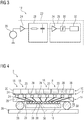
- An X-ray detector 2 described below is designed as a directly converting X-ray detector 2 and is shown in FIG FIG 1 shown schematically in a first embodiment.
- the X-ray detector 2 is part of an X-ray device 4, which is designed as a computer tomograph and is shown in FIG FIG 2 is sketched.
- the x-ray detector 2 is supplemented by an x-ray source 6.
- the x-ray device 4 has a control unit 8.
- the X-ray detector 2 is designed as a directly converting X-ray detector 2 and has a converter layer or sensor layer 10, a first amplifier stage 12, an interposer 14 and an ASIC readout chip 16 as essential components.
- the x-ray detector 2 has a multiplicity of pixels 18 or forms a multiplicity of pixels 18, a volume element 20 of the sensor layer 10 and a signal processing unit 22 belonging to each pixel 18
- FIG 3 such a pixel 18 is shown as an example in the form of a simplified block diagram.
- Each signal processing unit 22 in turn is formed in the exemplary embodiment by a first amplifier circuit 24, which is part of the first amplifier stage 12, and a readout circuit 26, which is part of the ASIC readout chip 16, the first amplifier circuit 24 via an interposer connection 28 , which is part of the interposer 14, is connected to the readout circuit 26.
- Pixel 18 has a volume element 20 and a signal processing unit 22 with a first amplifier circuit 24, with an interposer connection 28 and with a readout circuit 26.
- Such an interposer connection 28 typically has a characteristic parasitic capacitance and a characteristic parasitic resistance.
- a sensor signal generated in a volume element 20 of a pixel 18 is first amplified in the first amplifier circuit 24 of the corresponding pixel 18, which is connected to the volume element 20.
- the amplified sensor signal is then forwarded via the interposer connection 28 of this pixel 18 to the ASIC readout chip 16 and processed there in the readout circuit 26 of the pixel 18.
- the signal processing units 22 of the pixels 18 work independently of one another and the X-ray quanta impinging on each pixel 18 are counted, the readout circuit 26 in the ASIC readout chip 16 typically having a comparator 30 and a counting unit 32 for this purpose.
- each readout circuit 26 has a second amplifier circuit 34, and all second amplifier circuits 34 of the ASIC readout chip 16 together form a second amplifier stage.
- FIG 1 a first variant embodiment of the X-ray detector 2 is now shown schematically in a partial sectional view. It can be seen from the illustration that the interposer 14 is interposed between the sensor layer 10 and the ASIC readout chip 16 and that the ASIC readout chip 16 is finally connected in an electrically conductive manner to a circuit board 36 or is connected to the circuit board 36.
- first amplifier stage 12 is interposed between the sensor layer 10 and the interposer 14, with between the sensor layer 10 and the first amplifier stage 12 in the exemplary embodiment simple soldered connections 38 are formed.
- a volume element 20 is connected in an electrically conductive manner to a first amplifier circuit 24 of the first amplifier stage 12 via such a soldered connection 38.
- the first amplifier stage 12 is implemented, for example, on a film that is not explicitly shown, that is, for example, printed on a film, and the film is then laminated, for example, onto the sensor layer 10 or the interposer 14.
- the first amplifier stage 12 is manufactured using a method based on TFT technology and implemented on the interposer 14, which is then preferably designed as a glass interposer.
- FIG. 4 A second variant embodiment of the X-ray detector 2 is shown in FIG FIG 4 shown, at least in a simplified form.
- the first amplifier stage 12 is formed directly on the sensor layer 10, for this purpose a silicon layer or silicon layer is applied to the sensor layer 10 by epitaxy for this purpose and the semiconductor circuits (not shown) that form the first amplifier stage 12 are integrated into this silicon layer or in the silicon layer are realized.
- Silicon is only a suitable example of material.
- gallium arsenide is used as the sensor material of the sensor layer 10
- FIG. 5 Another variant of the X-ray detector 2 is shown in FIG FIG 5 indicated.
- several layers 40, 41, 42 namely a first layer 40, an intermediate layer 41 and a redistribution layer 42, are attached to the sensor layer 10, the first amplifier stage 12 being implemented in the intermediate layer 41. Since the contacting in the embodiment according to FIG 5 ultimately takes place across all three layers 40, 41, 42 shown, in principle all three layers 40, 41, 42 in this exemplary embodiment form the interposer 14, the first amplifier stage 12 being formed in the intermediate layer 41 of this interposer 14.
- FIG 5 It is shown in FIG 5 a basic structure in the area of a pixel 18.
- the volume element 20 of the pixel is initially followed by a metal contact 44. That metal contact 44 is embedded in the first layer 40 made of silicon.
- This first layer 40 is followed by two further layers of silicon, circuit structures 46 which form the first amplifier circuit 24 of this pixel 18 being formed in the intermediate layer 41 by doping.
- the third layer 42 which serves as a redistribution layer 42, has conductor tracks 48 made of copper 48, through which an output 50 of the interposer, which is led to the outside, is positioned such that it is directly connected to an input on the ASIC readout chip 16 via a soldered connection 38 Can be connected in an electrically conductive manner and is also connected in the X-ray detector 2.
- the third embodiment of the X-ray detector 2 according to FIG FIG 5 is furthermore adapted in some cases to the effect that the intermediate layer 41 is replaced by several comparable intermediate layers / intermediate layers.
- the reason for this is then typically that additional wiring, for example for power supply and / or for distributing the signals, is also implemented for the first amplifier circuit 24. Such wiring is then often implemented in several layers.
- FIG. 6 A fourth exemplary embodiment of the X-ray detector 2 is shown in FIG FIG 6 shown schematically.
- the ASIC readout chip 16 is connected to the first amplifier stage 12 via a partly flexible partly rigid circuit board 52, this circuit board 52 functioning as a type of interposer 14.
- the first amplifier stage 12 itself is not more detailed vias shown and soldered connections 38 are electrically conductively connected to the sensor layer 10.
- the first amplifier stage 12 is implemented on a thin, rigid first part 54 of the circuit board 52. It is manufactured in a simple and inexpensive circuit process. That first part 54 of the circuit board 52 is connected via a flexible, second part 56 to another rigid third part 58 to which the ASIC readout chip 16 is connected.
- the ASIC readout chip 16 is manufactured in a more complex and expensive process and implemented on a significantly smaller area.
Abstract
Die Erfindung betrifft einen Röntgendetektor (2) aufweisend eine Sensorschicht (10) zur direkten Konvertierung von Röntgenstrahlung und einen nachgeschalteten Auslesechip (16), wobei zwischen Sensorschicht (10) und Auslesechip (16) eine erste Verstärkerstufe (12) zwischengeschaltet ist.The invention relates to an X-ray detector (2) having a sensor layer (10) for direct conversion of X-rays and a downstream readout chip (16), a first amplifier stage (12) being interposed between the sensor layer (10) and readout chip (16).
Description
Die Erfindung betrifft einen Röntgendetektor aufweisend eine Sensorschicht und einen nachgeschalteten Auslesechip. Darüber hinaus betrifft die Erfindung ein Röntgengerät mit einem solchen Röntgendetektor.The invention relates to an X-ray detector having a sensor layer and a downstream readout chip. The invention also relates to an x-ray device with such an x-ray detector.
In bilderzeugenden Röntgengeräten werden zunehmend sogenannte direkt konvertierende Röntgendetektoren eingesetzt, wie sie zum Beispiel in der
Hierbei ist aktuell der Auslesechip direkt an die Sensorschicht angekoppelt, so dass die sehr kleinen analogen Signal-Pulse, welche durch Röntgenquanten im Sensormaterial der Sensorschicht generiert werden, möglichst unverfälscht und rauscharm in den Auslesechip gelangen und dort verarbeitet oder vermessen werden können. Dabei ist eingangsseitig im Auslesechip eine Verstärkerstufe geschaltet, die diese Signal-Pulse verstärkt und so für die weitere Verarbeitung im Auslesechip robust gegen Störeinflüsse macht.The readout chip is currently coupled directly to the sensor layer, so that the very small analog signal pulses generated by X-ray quanta in the sensor material of the sensor layer get into the readout chip as unadulterated and with low noise as possible and can be processed or measured there. An amplifier stage is connected to the input side in the readout chip, which amplifies these signal pulses and thus makes them robust against interference for further processing in the readout chip.
Um nun bei einem solchen Röntgendetektor eine große Sensorfläche zu realisieren, werden typischerweise mehrere Untereinheiten, sogenannte Sensorboards, eng aneinander gekachelt. Für die Bildgebung ist es dabei essenziell, dass der Aufbau des Röntgendetektor oder vielmehr der Sensorfläche möglichst spaltfrei erfolgt. Um dies zu ermöglichen werden üblicherweise Durchkontaktierungen, sogenannte TSVs, in den Auslesechip eingebracht, da dann die Untereinheiten problemlos auch vierseitig direkt aneinandergereiht werden können. Die Herstellung von Auslesechips mit Durchkontaktierungen ist jedoch sehr aufwändig und infolgedessen auch kostenintensiv.In order to realize a large sensor surface with such an X-ray detector, several sub-units, so-called sensor boards, are typically tiled close together. For imaging, it is essential that the X-ray detector, or rather the sensor surface, is constructed with as little gaps as possible. In order to make this possible, vias, so-called TSVs, are usually introduced into the readout chip, since the sub-units can then also be lined up directly on four sides without any problems. However, the production of readout chips with plated-through holes is very complex and consequently also cost-intensive.
Wählt man dagegen andere Ansätze zur Kontaktierung des Auslesechips, bei denen der Auslesechip nicht direkt an die Sensorschicht angekoppelt ist, besteht das Problem, dass längere Leitungen oder gar unterschiedliche Leitungslängen für verschiedene Pixel das Antwortverhalten des Auslesechips stark beeinflussen. Dies kann so weit gehen, dass die Bildqualität problematisch beeinflusst wird.If, on the other hand, one chooses other approaches to contacting the readout chip in which the readout chip is not directly coupled to the sensor layer, the problem arises that longer lines or even different line lengths for different pixels have a strong influence on the response behavior of the readout chip. This can go so far that the image quality is problematically affected.
Ausgehend hiervon liegt der Erfindung die Aufgabe zugrunde, einen vorteilhaft ausgestalteten Röntgendetektor sowie ein vorteilhaft ausgestaltetes Röntgengerät mit einem entsprechenden Röntgendetektor anzugeben.Proceeding from this, the invention is based on the object of specifying an advantageously designed x-ray detector and an advantageously designed x-ray device with a corresponding x-ray detector.
Diese Aufgabe wird erfindungsgemäß gelöst durch einen Röntgendetektor mit den Merkmalen des Anspruchs 1 sowie durch ein Röntgengerät mit den Merkmalen des Anspruchs 15. Die rückbezogenen Ansprüche beinhalten teilweise vorteilhafte und teilweise für sich selbst erfinderische Weiterbildungen dieser Erfindung. Die im Hinblick auf den Röntgendetektor angeführten Vorteile und bevorzugten Ausgestaltungen sind sinngemäß auch auf das Röntgengerät übertragbar und umgekehrt.According to the invention, this object is achieved by an X-ray detector with the features of claim 1 and by an X-ray device with the features of claim 15. The claims referring back to the invention contain partly advantageous and partly inventive developments of this invention. The advantages and preferred embodiments cited with regard to the X-ray detector can also be applied to the X-ray device and vice versa.
Der erfindungsgemäße Röntgendetektor ist dabei zweckdienlicherweise ausgebildet für eine Nutzung in einem Röntgengerät, beispielsweise einem Computertomographen, und weist eine Sensorschicht sowie einen nachgeschalteten Auslesechip auf, wobei der Auslesechip bevorzugt als sogenannter ASIC-Auslesechip (ASIC:application-specific integrated circuit) ausgestaltet ist.The x-ray detector according to the invention is expediently designed for use in an x-ray device, for example a computer tomograph, and has a sensor layer and a downstream readout chip, the readout chip preferably being designed as a so-called ASIC readout chip (ASIC: application-specific integrated circuit).
Hierbei ist der Röntgendetektor und/oder die Sensorschicht typischerweise aus mehreren Untereinheiten oder Modulen aufgebaut, die üblicherweise im Wesentlichen identisch ausgestaltet sind. Ist der Röntgendetektor aus Modulen aufgebaut, so weist üblicherweise jedes Röntgendetektor-Modul eine entsprechende Sensorschicht und zumindest einen entsprechenden nachgeschalteten Auslesechip auf.In this case, the X-ray detector and / or the sensor layer is typically constructed from a plurality of sub-units or modules, which are usually designed essentially identically. If the X-ray detector is made up of modules, each X-ray detector module usually has a corresponding sensor layer and at least one corresponding readout chip connected downstream.
Unabhängig davon, ob nun ein modularer Aufbau vorliegt oder nicht, ist erfindungsgemäß zwischen der Sensorschicht und dem Auslesechip eine erste Verstärkerstufe zwischengeschaltet, wobei diese erste Verstärkerstufe zweckdienlicherweise ebenfalls als eine Art Schicht, also eine Art funktionelle Schicht, ausgebildet ist. Die erste Verstärkerstufe ist dabei typischerweise direkt oder unmittelbar an der Sensorschicht platziert und insbesondere direkt oder unmittelbar mit dieser elektrisch leitfähig verbunden, beispielsweise über Lötverbindungen.Regardless of whether there is a modular structure or not, according to the invention a first amplifier stage is interposed between the sensor layer and the readout chip, this first amplifier stage also being expediently designed as a type of layer, i.e. a type of functional layer. The first amplifier stage is typically placed directly or directly on the sensor layer and, in particular, directly or directly connected to it in an electrically conductive manner, for example via soldered connections.
Dabei ist die erste Verstärkerstufe bevorzugt über sehr kurze und insbesondere gleichartige elektrisch leitfähige Verbindungen oder Überbrückungen, also insbesondere Lötverbindungen, mit der Sensorschicht verbunden, sodass diese elektrisch leitfähigen Verbindungen keine signifikanten parasitären Kapazitäten und/oder Widerstände aufweisen. Durch die erste Verstärkerstufe werden dann im Betrieb des Röntgendetektors die Sensorsignale oder Sensor-Pulse aus der Sensorschicht durch die erste Verstärkerstufe verstärkt, noch bevor parasitäre Kapazitäten und/oder Widerstände wirksam werden und in der Folge sind dann die verstärkten Sensorsignale unempfindlicher gegen Effekte von parasitären Kapazitäten und/oder Widerständen in der elektrisch leitfähige Verbindung hin zum Auslesechip.The first amplifier stage is preferably connected to the sensor layer via very short and, in particular, similar electrically conductive connections or bridges, that is to say in particular soldered connections, so that these electrically conductive connections do not have any significant parasitic capacitances and / or resistances. The first amplifier stage then amplifies the sensor signals or sensor pulses from the sensor layer through the first amplifier stage when the X-ray detector is in operation, even before parasitic capacitances and / or resistances become effective and as a result the amplified sensor signals are then less sensitive to the effects of parasitic capacitances and / or resistors in the electrically conductive connection to the readout chip.
Somit werden dann die verstärkten Sensorsignale nahezu unbeeinträchtigt von den weiteren Leitungslängen und/oder den weiteren Leitungskapazitäten an den Auslesechip herangeführt und dort weiterverarbeitet. Hierdurch ergeben sich neue Möglichkeiten hinsichtlich der Ausgestaltung der elektrisch leitfähigen Verbindungen hin zum Auslesechip. Dabei wird es insbesondere ermöglicht, unabhängiger von den Eingangskapazitäten hin zu den Eingängen des Auslesechips zu werden.Thus, the amplified sensor signals are then fed to the readout chip almost unaffected by the further line lengths and / or the further line capacitances and are further processed there. This results in new possibilities with regard to the design of the electrically conductive connections to the readout chip. This makes it possible in particular to become more independent of the input capacities towards the inputs of the readout chip.
Die Grundidee kann hierbei auch darin gesehen werden, dass ausgehend von einem Röntgendetektor mit einem Auslesechip nach dem Stand der Technik eine Verlagerung der Verstärkerfunktion oder zumindest eines Teils der Verstärkerfunktion des Auslesechips aus dem Auslesechip heraus in eine weitere oder separate Komponentenebene vorgenommen wird. Diese neue, separate Komponentenebene wird dabei nahe der Sensorschicht platziert. Dies ermöglicht eine weite räumliche Trennung von Sensorschicht und Auslesechip unter Berücksichtigung der Problematik, dass die Sensorschicht sehr kleine analoge Sensorsignale im pA-Bereich liefert, aber dennoch eine genaue Detektion/Auswertung der Sensorsignale im Auslesechip erfolgen soll.The basic idea here can also be seen in the fact that, based on an X-ray detector with a readout chip according to the prior art, the amplifier function is shifted or at least part of the amplifier function of the readout chip is performed from the readout chip into a further or separate component level. This new, separate component level is placed near the sensor layer. This enables a wide spatial separation of the sensor layer and readout chip, taking into account the problem that the sensor layer delivers very small analog sensor signals in the pA range, but precise detection / evaluation of the sensor signals should still take place in the readout chip.
Weiter ist der Röntgendetektor als sogenannter direkt konvertierender Röntgendetektor oder Photonenzählender Röntgendetektor ausgebildet und dementsprechend ist beispielsweise CdTe, CdZnTe, CdZnTeSe, CdTeSe, CdNnTe, InP, TIBr2, oder HgI2 Hauptbestandteil der Sensorschicht. Die Sensorschicht oder Konverterschicht dient dabei nach an sich bekanntem Prinzip zur direkten Konvertierung von Röntgenstrahlung in elektrische Signale, also Sensorsignale, wobei die Sensorsignale typischerweise als Strom-Pulse vorliegen.Furthermore, the X-ray detector is designed as a so-called directly converting X-ray detector or photon-counting X-ray detector and accordingly, for example, CdTe, CdZnTe, CdZnTeSe, CdTeSe, CdNnTe, InP, TIBr 2 , or HgI 2 is the main component of the sensor layer. The sensor layer or converter layer is used according to a principle known per se for the direct conversion of X-ray radiation into electrical signals, that is to say sensor signals, the sensor signals typically being present as current pulses.
Außerdem weist der Röntgendetektor oder ein jedes Röntgendetektor-Modul zweckdienlicherweise eine Vielzahl von Pixeln auf, wobei zu jedem Pixel typischerweise ein Volumenelement der Sensorschicht gehört sowie eine daran elektrisch leitfähig angebundene Signalverarbeitungs-Einheit. Teil einer solchen Signalverarbeitungs-Einheit ist dabei in der Regel eine Verstärkerschaltung der ersten Verstärkerstufe und eine Ausleseschaltung im Auslesechip. Hierbei werden die in der Sensorschicht generierten Sensorsignale der verschiedenen Pixel typischerweise zumindest anfangs unabhängig voneinander verstärkt, verarbeitet und ausgewertet und dementsprechend weist dann die erste Verstärkerstufe üblicherweise für jedes Pixel eine eigene Verstärkerschaltung auf und der Auslesechip weist typischerweise einen Signaleingang pro Pixel auf. Es findet also insbesondere eine pixelweise Verstärkung durch die erste Verstärkerstufe statt.In addition, the x-ray detector or each x-ray detector module expediently has a multiplicity of pixels, with each pixel typically including a volume element of the sensor layer and a signal processing unit connected to it in an electrically conductive manner. Part of such a signal processing unit is usually an amplifier circuit of the first amplifier stage and a readout circuit in the readout chip. In this case, the sensor signals generated in the sensor layer of the various pixels are typically amplified, processed and evaluated independently of one another at least initially, and accordingly the first amplifier stage then usually has its own amplifier circuit for each pixel and the readout chip typically has one signal input per pixel. In particular, there is therefore a pixel-wise amplification by the first amplifier stage.
Die Verstärkerschaltungen der ersten Verstärkerstufe sind hierbei typischerweise mittels einfacher TransistorSchaltungen realisiert, die in den meisten Fällen durch Nutzung einer CMOS-Technologie hergestellt sind. Davon unabhängig wird je nach Anwendungsfall mittels einer entsprechenden Verstärkerschaltung eine Stromverstärkung mit einem Verstärkungsfaktor realisiert, dessen Wert im Bereich von etwa 2 bis etwa 100 und insbesondere im Bereich von etwa 2 bis etwa 50 liegt. Alternativ oder ergänzend hierzu wird in der ersten Verstärkerstufe eine Strom-zu-Spannungswandlung realisiert, wobei in diesem Fall die Stromwerte vorzugsweise mit einem Faktor im Bereich von etwa 1 mV/nA bis etwa 100 mV/nA und insbesondere im Bereich von etwa 1 mV/nA bis etwa 50 mV/nA in Spannungswerte umgewandelt werden.The amplifier circuits of the first amplifier stage are typically implemented using simple transistor circuits, which in most cases are produced using CMOS technology. Independently of this, depending on the application, a current gain with a gain factor is implemented by means of a corresponding amplifier circuit, the value of which is in the range from approximately 2 to approximately 100 and in particular in the range from approximately 2 to approximately 50. As an alternative or in addition to this, a current-to-voltage conversion is implemented in the first amplifier stage, in which case the current values are preferably with a factor in the range from about 1 mV / nA to about 100 mV / nA and in particular in the range from about 1 mV / nA to about 50 mV / nA can be converted into voltage values.
In jedem Fall aber wird mittels der ersten Verstärkerstufe bevorzugt eine aktive Verstärkung vorgenommen und dementsprechend wird die erste Verstärkerstufe im Betrieb mit elektrischer Leistung versorgt. D. h., dass die erste Verstärkerstufe einen Versorgungseingang für elektrische Leistung aufweist, über die im Betrieb der ersten Verstärkerstufe elektrische Leistung zur aktiven Verstärkung von Sensorsignalen zugeführt wird.In any case, however, active amplification is preferably carried out by means of the first amplifier stage and the first amplifier stage is accordingly supplied with electrical power during operation. That is to say that the first amplifier stage has a supply input for electrical power, via which electrical power for the active amplification of sensor signals is supplied during operation of the first amplifier stage.
Gemäß einer bevorzugten Ausgestaltung des Röntgendetektors weist der Auslesechip zudem eine zweite Verstärkerstufe auf, die in den Auslesechip integriert ist und somit Teil des Auslesechips ist. Die zweite Verstärkerstufe weist dabei typischerweise eine Verstärkerschaltung pro Pixel auf, wobei eine jede solche Verstärkerschaltung typischerweise einem Eingang unmittelbar nachgeschaltet ist. Die Verstärkerschaltungen der zweiten Verstärkerstufe sind hierbei vorzugsweise einfacher gehalten als bei einem Auslesechip nach dem Stand der Technik, da ja bereits durch die erste Verstärkerstufe im Betrieb eine Verstärkung erfolgt.According to a preferred embodiment of the X-ray detector, the readout chip also has a second amplifier stage which is integrated into the readout chip and is therefore part of the readout chip. The second amplifier stage typically has one amplifier circuit per pixel, each such amplifier circuit typically being connected immediately after an input. The amplifier circuits of the second amplifier stage are preferably kept simpler than in the case of a read-out chip according to the prior art, since amplification already takes place during operation by the first amplifier stage.
Die mit einer Verstärkerschaltung der zweiten Verstärkerstufe realisierte Verstärkung richtet sich dabei üblicherweise nach der durch die erste Verstärkerstufe realisierten Verstärkung und/oder danach, ob mittels der ersten Verstärkerstufe eine Strom-zu-Spannungswandlung realisiert ist oder wird. Hierbei ist die zweite Verstärkerstufe bevorzugt derart ausgestaltet, dass spätestens an den Ausgängen der zweiten Verstärkerstufe Spannungssignale vorliegen und zwar insbesondere Spannungssignale, deren typische Pulshöhen je nach Energie der Röntgenquanten im Bereich von etwa 10 mV bis etwa 150 mV liegen. Je nach Auslegung, also beispielsweise je nach gewählten Herstellungsprozess und dessen bevorzugter Betriebsspannung sowie der geforderten Linearität (Vermeidung von Sättigung durch sogenanntes Pile-Up), schwanken diese Werte gegebenenfalls noch um einen Faktor bis etwa 5. Der typischerweise sehr große Schwankungsbereich wird dabei häufig durch viele unterschiedliche Faktoren beeinflusst.The gain realized with an amplifier circuit of the second amplifier stage is usually based on this the gain realized by the first amplifier stage and / or according to whether a current-to-voltage conversion is or will be realized by means of the first amplifier stage. The second amplifier stage is preferably designed in such a way that voltage signals are present at the latest at the outputs of the second amplifier stage, in particular voltage signals whose typical pulse heights are in the range of about 10 mV to about 150 mV, depending on the energy of the X-ray quanta. Depending on the design, e.g. depending on the selected manufacturing process and its preferred operating voltage as well as the required linearity (avoidance of saturation by so-called pile-up), these values may fluctuate by a factor of up to about 5.The typically very large fluctuation range is often due to influences many different factors.
Da sich also die mit einer Verstärkerschaltung der zweiten Verstärkerstufe realisierte Verstärkung vorzugsweise nach der Ausgestaltung der ersten Verstärkerstufe richtet, wird in einigen Fällen sogar auf eine größere oder gar auf eine gezielte Verstärkung mittels der zweiten Verstärkerstufe verzichtet. In einem solchen Fall erfolgt durch eine Verstärkerschaltung der zweiten Verstärkerstufe vor allem eine Filterung des mittels der ersten Verstärkerstufe verstärkten Signals, welche auch als Pulsformung bezeichnet wird, und/oder eine Strom-zu-Spannungswandlung. Typische Verstärkungsfaktoren liegen dann lediglich im Bereich von etwa 1 bis etwa 10.Since the gain realized with an amplifier circuit of the second amplifier stage is preferably based on the design of the first amplifier stage, in some cases even a larger or even targeted gain by means of the second amplifier stage is dispensed with. In such a case, an amplifier circuit of the second amplifier stage primarily filters the signal amplified by means of the first amplifier stage, which is also referred to as pulse shaping, and / or a current-to-voltage conversion. Typical gain factors are then only in the range from about 1 to about 10.
Weiter weist der Auslesechip üblicherweise eine Filterschaltung pro Pixel auf, die typischerweise der Verstärkerschaltung der zweiten Verstärkerstufe nachgeschaltet ist. Außerdem weist der Auslesechip üblicherweise eine Zählerschaltung pro Pixel auf, die dann typischerweise die pixelweise Verarbeitung der Sensorsignale abschließt.Furthermore, the readout chip usually has one filter circuit per pixel, which is typically connected downstream of the amplifier circuit of the second amplifier stage. In addition, the readout chip usually has a counter circuit per pixel, which then typically completes the processing of the sensor signals pixel by pixel.
Von Vorteil ist des Weiteren eine Ausführung des Röntgendetektors, bei der zwischen der Sensorschicht und dem Auslesechip ein sogenannter Interposer zwischengeschaltet ist. Der Interposer, auch Umverdrahtungseinheit oder Umkontaktierungseinheit genannt, dient dabei dazu, zwei Einheiten elektrisch leitfähig miteinander zu verbinden, die jeweils mehrere elektrische Kontakte oder Anschlüsse aufweisen, bei denen die elektrischen Kontakte oder Anschlüsse jedoch unterschiedlich angeordnet sind, sodass einfache direkte Verbindungen, beispielsweise Lötverbindungen, nicht ausgebildet werden können.Furthermore, an embodiment of the X-ray detector is advantageous in which between the sensor layer and the readout chip a so-called interposer is connected. The interposer, also called rewiring unit or re-contacting unit, serves to connect two units to one another in an electrically conductive manner, each of which has several electrical contacts or connections, but in which the electrical contacts or connections are arranged differently, so that simple direct connections, for example soldered connections, cannot be trained.
Ist ein solcher Interposer vorgesehen, so ist dieser weiter bevorzugt der ersten Verstärkerstufe nachgeschaltet und dementsprechend ist dann die erste Verstärkerstufe bevorzugt zwischen Sensorschicht und Interposer zwischengeschaltet.If such an interposer is provided, it is more preferably connected downstream of the first amplifier stage and accordingly the first amplifier stage is then preferably connected between the sensor layer and the interposer.
Gemäß einer Ausführungsvariante ist die erste Verstärkerstufe weiter mittels eines Verfahrens auf Basis einer TFT-Technologie (TFT: thin-film transistor) gefertigt. Diese Technologie ermöglicht es, Transistoren auf Glas zu fertigen, und wird bereits in Großserie eingesetzt, zum Beispiel zur Fertigung von Displays.According to one embodiment variant, the first amplifier stage is also manufactured by means of a method based on TFT technology (TFT: thin-film transistor). This technology makes it possible to manufacture transistors on glass and is already being used in large-scale production, for example for the manufacture of displays.
Insbesondere wenn die erste Verstärkerstufe auf Basis einer TFT-Technologie gefertigt ist, ist es außerdem von Vorteil, wenn der Interposer als ein Glas-Interposer ausgestaltet ist, wobei dann weiter bevorzugt die erste Verstärkerstufe auf dem Glas-Interposer mittels eines Verfahrens auf Basis einer TFT-Technologie gefertigt ist. Dabei sind Technologien zur Fertigung von Durchkontaktierungen und/oder Umverdrahtungsebenen in Glas bereits verfügbar und reine Interposer aus Glas (ohne Verstärkerstufe) sind bereits bekannt. Diese Technologien werden nun im Falle einer Ausführungsvariante des Röntgendetektors genutzt, um einen Interposer aus Glas zu fertigen, der zusätzlich die erste Verstärkerstufe aufweist.In particular if the first amplifier stage is manufactured on the basis of TFT technology, it is also advantageous if the interposer is designed as a glass interposer, the first amplifier stage on the glass interposer then preferably using a method based on a TFT -Technology is manufactured. Technologies for the production of plated-through holes and / or rewiring levels in glass are already available and pure interposers made of glass (without an amplifier stage) are already known. In the case of an embodiment of the X-ray detector, these technologies are now used to manufacture an interposer made of glass, which also has the first amplifier stage.
Alternativ wird anstatt einem Interposer aus Glas ein Interposer auf der Basis eines Halbleitermaterials, beispielsweise Silizium, genutzt und in diesem Fall weist dann der Röntgendetektor einen solchen Interposer auf der Basis eines Halbleitermaterials auf. Ein derartige Interposer ist dann typischerweise aus mehreren Schichten oder Lagen aufgebaut und bevorzugt ist die erste Verstärkerstufe durch zumindest eine dieser Lagen ausgebildet.Alternatively, instead of an interposer made of glass, an interposer based on a semiconductor material, for example silicon, is used and in this case the x-ray detector then has such an interposer based on a semiconductor material on. Such an interposer is then typically made up of several layers or plies, and the first amplifier stage is preferably formed by at least one of these plies.
In vorteilhafter Weiterbildung ist der die erste Verstärkerstufe ausbildenden Lage des Interposers eine Umverteilungs-Lage (RDL: Re-Distribution-Layer) nachgeschaltet und üblicherweise sind alle Umverteilungs-Lagen des Interposers der die erste Verstärkerstufe ausbildenden Lage nachgeschaltet.In an advantageous further development, the position of the interposer forming the first amplifier stage is followed by a redistribution layer (RDL: re-distribution layer) and usually all redistribution positions of the interposer are connected downstream of the position forming the first amplifier stage.
Der Interposer besteht dann also beispielsweise aus mehreren Lagen, wobei eine Lage aus Silizium als Basismaterial ausgebildet ist und wobei in diese Lage die erste Verstärkerstufe integriert ist. Hierzu lässt sich zum Beispiel eine CMOS-Technologie nutzen, mittels der Verstärkerschaltungen einzeln oder in Gruppen von mehreren Verstärkern in Lagen des Interposers integriert werden. Diese Lagen haben hierzu typischerweise Aussparungen. Zudem weist ein solcher Interposer üblicherweise zumindest eine Umverteilungs-Lage auf, in der zum Beispiel Leiterbahnen aus Kupfer verlaufen.The interposer then consists, for example, of several layers, with one layer made of silicon being formed as the base material and with the first amplifier stage being integrated into this layer. For this purpose, for example, CMOS technology can be used, by means of which amplifier circuits are integrated individually or in groups of several amplifiers in layers of the interposer. These layers typically have cutouts for this purpose. In addition, such an interposer usually has at least one redistribution layer in which, for example, conductor tracks made of copper run.
Des Weiteren ist eine Ausführungsvariante des Röntgendetektors von Vorteil, bei der die erste Verstärkerstufe auf einer Folie realisiert ist. Hierbei ist die erste Verstärkerstufe bevorzugt auf die Folie aufgedruckt und dementsprechend sind dann die elektrischen und/oder elektronischen Bausteine der Verstärkerstufe durch eine Drucktechnik auf die Folie aufgebracht.Furthermore, an embodiment of the X-ray detector is advantageous in which the first amplifier stage is implemented on a film. In this case, the first amplifier stage is preferably printed onto the film and accordingly the electrical and / or electronic components of the amplifier stage are then applied to the film using a printing technique.
Eine solche Folie ist dann zweckdienlicherweise auf die Sensorschicht oder, sofern vorhanden, auf einen Interposer auflaminiert, also zum Beispiel aufgeklebt. Bevorzugt erfolgt die Befestigung mittels einer Art Klebung, wobei für elektrische Kontakte vorzugsweise ein Leitkleber genutzt wird.Such a film is then expediently laminated onto the sensor layer or, if present, onto an interposer, that is to say glued on, for example. The attachment preferably takes place by means of a type of adhesive bonding, a conductive adhesive preferably being used for electrical contacts.
Als vorteilhaft wird weiter eine Ausführungsvariante des Röntgendetektors angesehen, bei der die erste Verstärkerstufe an der Sensorschicht angebracht ist. Die erste Verstärkerstufe ist in diesem Fall bevorzugt durch eine Halbleiterschicht oder Halbleiterlage realisiert, die insbesondere durch Epilepsie auf die Sensorschicht aufgebracht ist, also entweder direkt oder indirekt über eine Zwischenlage oder Zwischenschicht.Another embodiment of the X-ray detector in which the first amplifier stage is considered advantageous is attached to the sensor layer. In this case, the first amplifier stage is preferably implemented by a semiconductor layer or semiconductor layer that is applied to the sensor layer in particular by epilepsy, that is to say either directly or indirectly via an intermediate layer or intermediate layer.
Es wird also zum Beispiel eine Siliziumschicht oder Siliziumlage durch Epitaxie auf der Sensorschicht abgeschieden und in diese Siliziumschicht wird dann die erste Verstärkerstufe implantiert. Hierbei wird je nach Anwendungsfall gegebenenfalls zunächst eine Zwischenlage aus Siliziumdioxid auf der Sensorschicht abgeschieden und nachfolgend wird dann die Siliziumschicht ausgebildet.For example, a silicon layer or silicon layer is deposited on the sensor layer by epitaxy, and the first amplifier stage is then implanted into this silicon layer. Here, depending on the application, an intermediate layer of silicon dioxide is first deposited on the sensor layer and then the silicon layer is then formed.
Zweckdienlich ist zudem eine Ausführungsvariante des Röntgendetektors, bei der zwischen der ersten Verstärkerstufe und dem Auslesechip eine Leiterplatte zwischengeschaltet ist. Die Leiterplatte ist dabei je nach Ausführungsvariante als starre Leiterplatte, als flexible Leiterplatte oder als teils starre und teils flexible Leiterplatte ausgebildet.An embodiment variant of the X-ray detector in which a circuit board is interposed between the first amplifier stage and the readout chip is also expedient. The circuit board is designed as a rigid circuit board, as a flexible circuit board or as a partly rigid and partly flexible circuit board, depending on the variant.
Ausführungsbeispiele der Erfindung werden nachfolgend anhand einer schematischen Zeichnung näher erläutert. Darin zeigen:
- FIG 1
- in einer ausschnittsweisen Schnittdarstellung eine erste Ausführung eines Röntgendetektors,
- FIG 2
- in einer semitransparenten Ansicht ein Röntgengerät mit dem Röntgendetektor,
- FIG 3
- in einem Schaltbild ein Pixel des Röntgendetektors,
- FIG 4
- in einer ausschnittsweisen Schnittdarstellung eine zweite Ausführung des Röntgendetektors,
- FIG 5
- in einer ausschnittsweisen Schnittdarstellung eine dritte Ausführung des Röntgendetektors und
- FIG 6
- in einer ausschnittsweisen Schnittdarstellung eine vierte Ausführung des Röntgendetektors.
- FIG 1
- a partial sectional view of a first embodiment of an X-ray detector,
- FIG 2
- an X-ray device with the X-ray detector in a semi-transparent view,
- FIG 3
- a pixel of the X-ray detector in a circuit diagram,
- FIG 4
- a second embodiment of the X-ray detector in a partial sectional view,
- FIG 5
- a third embodiment of the X-ray detector and in a partial sectional illustration
- FIG 6
- a fourth embodiment of the X-ray detector in a partial sectional view.
Einander entsprechende Teile sind in allen Figuren jeweils mit den gleichen Bezugszeichen versehen.Corresponding parts are provided with the same reference symbols in each of the figures.
Ein nachfolgend beschriebener Röntgendetektor 2 ist als direkt konvertierender Röntgendetektor 2 ausgebildet und in
Im Ausführungsbeispiel ist der Röntgendetektor 2 dabei Bestandteil eines Röntgengeräts 4, welches exemplarisch als Computertomograph ausgebildet und in
Der Röntgendetektor 2 ist, wie bereits dargelegt, als direkt konvertierender Röntgendetektor 2 ausgestaltet und weist als wesentliche Komponenten eine Konverterschicht oder Sensorschicht 10, eine erste Verstärkerstufe 12, einen Interposer 14 sowie einen ASIC-Auslesechip 16 auf.As already explained, the
Außerdem weist der Röntgendetektor 2 eine Vielzahl an Pixeln 18 auf oder bildet eine Vielzahl an Pixeln 18 aus, wobei zu jedem Pixel 18 ein Volumenelement 20 der Sensorschicht 10 gehört sowie eine Signalverarbeitungs-Einheit 22. In
Eine jede Signalverarbeitungs-Einheit 22 wiederum wird im Ausführungsbeispiel gebildet durch eine erste Verstärkerschaltung 24, die Teil der ersten Verstärkerstufe 12 ist, sowie eine Ausleseschaltung 26, die Teil des ASIC-Auslesechips 16 ist, wobei die erste Verstärkerschaltung 24 über eine Interposer-Verbindung 28, die Teil des Interposers 14 ist, mit der Ausleseschaltung 26 verbunden ist. Somit weist also jedes Pixel 18 ein Volumenelement 20 sowie eine Signalverarbeitungs-Einheit 22 mit einer ersten Verstärkerschaltung 24, mit einer Interposer-Verbindung 28 sowie mit einer Ausleseschaltung 26 auf. Hierbei weist eine solche Interposer-Verbindung 28 typischerweise eine charakteristische parasitäre Kapazität sowie einen charakteristischen parasitären Widerstand auf.Each
Infolge dieser Ausgestaltung wird dann im Betrieb des Röntgendetektors 2 ein in einem Volumenelement 20 eines Pixels 18 generiertes Sensorsignal zunächst in der an das Volumenelement 20 angebundenen ersten Verstärkerschaltung 24 des entsprechenden Pixels 18 verstärkt. Nachfolgend wird das verstärkte Sensorsignal über die Interposer-Verbindung 28 dieses Pixels 18 hin zum ASIC-Auslesechips 16 weitergeleitet und dort in der Ausleseschaltung 26 des Pixels 18 weiterverarbeitet.As a result of this embodiment, when the
Im Ausführungsbeispiel arbeiten die Signalverarbeitungs-Einheiten 22 der Pixel 18 unabhängig voneinander und in jedem Pixel 18 werden die auftreffenden Röntgenquanten gezählt, wobei die Ausleseschaltung 26 im ASIC-Auslesechip 16 hierfür typischerweise einen Komparator 30 und eine Zähleinheit 32 aufweist. Zudem weist im Ausführungsbeispiel jede Ausleseschaltung 26 eine zweite Verstärkerschaltung 34 auf und alle zweiten Verstärkerschaltungen 34 des ASIC-Auslesechips 16 bilden zusammen eine zweite Verstärkerstufe aus.In the exemplary embodiment, the
In
Weiter ist zwischen Sensorschicht 10 und Interposer 14 die erste Verstärkerstufe 12 zwischengeschaltet, wobei zwischen der Sensorschicht 10 und der ersten Verstärkerstufe 12 im Ausführungsbeispiel einfache Lötverbindungen 38 ausgebildet sind. Dabei ist über eine solche Lötverbindung 38 ein Volumenelement 20 mit einer ersten Verstärkerschaltung 24 der ersten Verstärkerstufe 12 elektrisch leitfähig verbunden.Furthermore, the
Die erste Verstärkerstufe 12 ist hierbei je nach Ausgestaltungsvariante beispielsweise auf einer nicht explizit dargestellten Folie realisiert, also zum Beispiel auf eine Folie aufgedruckt, und die Folie ist dann zum Beispiel auf die Sensorschicht 10 oder den Interposer 14 auflaminiert.Depending on the design variant, the
Alternativ ist die erste Verstärkerstufe 12 mittels eines Verfahrens auf Basis einer TFT-Technologie gefertigt und auf dem Interposer 14 realisiert, der dann bevorzugt als Glas-Interposer ausgebildet ist.Alternatively, the
Eine zweite Ausführungsvariante des Röntgendetektors 2 ist in
Eine weitere Ausführungsvariante des Röntgendetektors 2 ist in
Gezeigt ist dabei in
Die dritte Ausführung des Röntgendetektors 2 gemäß
Ein viertes Ausführungsbeispiel des Röntgendetektors 2 ist in
Außerdem ist die erste Verstärkerstufe 12 auf einem dünnen, starren ersten Teil 54 der Leiterplatte 52 realisiert. Sie ist in einem einfachen und preisgünstigen Schaltkreisprozess gefertigt. Jener erste Teil 54 der Leiterplatte 52 ist über einen flexiblen, zweiten Teil 56 mit einem wiederum starren dritten Teil 58 verbunden, an dem der ASIC-Auslesechip 16 angebunden ist. Der ASIC-Auslesechip 16 ist in einem aufwändigeren und teureren Prozess gefertigt und auf einer wesentlich kleineren Fläche realisiert.In addition, the
Die Erfindung ist nicht auf das vorstehend beschriebene Ausführungsbeispiel beschränkt. Vielmehr können auch andere Varianten der Erfindung von dem Fachmann hieraus abgeleitet werden, ohne den Gegenstand der Erfindung zu verlassen. Insbesondere sind ferner alle im Zusammenhang mit dem Ausführungsbeispiel beschriebenen Einzelmerkmale auch auf andere Weise miteinander kombinierbar, ohne den Gegenstand der Erfindung zu verlassen.The invention is not restricted to the exemplary embodiment described above. Rather, other variants of the invention can also be derived from this by the person skilled in the art without departing from the subject matter of the invention. In particular, all of the individual features described in connection with the exemplary embodiment can also be combined with one another in other ways without departing from the subject matter of the invention.
Claims (15)
dadurch gekennzeichnet, dass zwischen Sensorschicht (10) und Auslesechip (16) eine erste Verstärkerstufe (12) zwischengeschaltet ist.X-ray detector (2) having a sensor layer (10) for direct conversion of X-rays and a downstream readout chip (16),
characterized in that a first amplifier stage (12) is interposed between the sensor layer (10) and the readout chip (16).
dadurch gekennzeichnet, dass der Auslesechip (16) eine zweite Verstärkerstufe (34) aufweist.X-ray detector (2) according to claim 1,
characterized in that the readout chip (16) has a second amplifier stage (34).
dadurch gekennzeichnet, dass zwischen Sensorschicht (20) und Auslesechip (16) ein Interposer (14) zwischengeschaltet ist.X-ray detector (2) according to claim 1 or 2,
characterized in that an interposer (14) is interposed between the sensor layer (20) and the readout chip (16).
dadurch gekennzeichnet, dass die erste Verstärkerstufe (12) zwischen Sensorschicht (10) und Interposer (14) zwischengeschaltet ist.X-ray detector (2) according to claim 3,
characterized in that the first amplifier stage (12) is interposed between the sensor layer (10) and the interposer (14).
dadurch gekennzeichnet, dass die erste Verstärkerstufe (12) mittels eines Verfahrens auf Basis einer TFT-Technologie gefertigt ist.X-ray detector (2) according to one of claims 1 to 4,
characterized in that the first amplifier stage (12) is manufactured by means of a method based on TFT technology.
dadurch gekennzeichnet, dass zwischen Sensorschicht (10) und Auslesechip (16) als Interposer (14) ein Glas-Interposer zwischengeschaltet ist und dass die erste Verstärkerstufe (12) auf dem Glas-Interposer mittels eines Verfahrens auf Basis einer TFT-Technologie gefertigt ist.X-ray detector (2) according to claim 3 or 4,
characterized in that a glass interposer is interposed as an interposer (14) between the sensor layer (10) and the readout chip (16) and that the first amplifier stage (12) is manufactured on the glass interposer by means of a process based on TFT technology.
dadurch gekennzeichnet, dass zwischen Sensorschicht (10) und Auslesechip (16) der Interposer (14) zwischengeschaltet ist, dass der Interposer (14) eine Anzahl Lagen (40,41,42) aufweist und dass die erste Verstärkerstufe (12) durch zumindest eine dieser Lagen (41) ausgebildet ist.X-ray detector (2) according to claim 3 or 4,
characterized in that the interposer (14) is interposed between the sensor layer (10) and the readout chip (16) is that the interposer (14) has a number of layers (40, 41, 42) and that the first amplifier stage (12) is formed by at least one of these layers (41).
dadurch gekennzeichnet, dass die die erste Verstärkerstufe (12) ausbildende Lage (41) einer Umverteilungs-Lage (42) vorgeschaltet ist.X-ray detector (2) according to claim 7,
characterized in that the layer (41) forming the first amplifier stage (12) is connected upstream of a redistribution layer (42).
dadurch gekennzeichnet, dass die erste Verstärkerstufe (12) auf einer Folie realisiert ist.X-ray detector (2) according to one of claims 1 to 4,
characterized in that the first amplifier stage (12) is implemented on a film.
dadurch gekennzeichnet, dass die erste Verstärkerstufe (12) auf die Folie aufgedruckt ist.X-ray detector (2) according to claim 9,
characterized in that the first amplifier stage (12) is printed onto the film.
dadurch gekennzeichnet, dass die Folie auf die Sensorschicht (12) oder einen Interposer (14) auflaminiert ist.X-ray detector (2) according to claim 9 or 10,
characterized in that the film is laminated onto the sensor layer (12) or an interposer (14).
dadurch gekennzeichnet, dass die erste Verstärkerstufe (12) an der Sensorschicht (10) angebracht ist.X-ray detector (2) according to one of claims 1 to 4,
characterized in that the first amplifier stage (12) is attached to the sensor layer (10).
dadurch gekennzeichnet, dass die erste Verstärkerstufe (12) mittels einer Halbleiterschicht (41) realisiert ist, die durch Epitaxie auf die Sensorschicht (10) aufgebracht ist.X-ray detector (2) according to one of claims 1 to 4,
characterized in that the first amplifier stage (12) is implemented by means of a semiconductor layer (41) which is applied to the sensor layer (10) by epitaxy.
dadurch gekennzeichnet, dass zwischen der ersten Verstärkerstufe (12) und dem Auslesechip (16) eine Leiterplatte (52) zwischengeschaltet ist.X-ray detector (2) according to claim 12 or 13,
characterized in that a printed circuit board (52) is interposed between the first amplifier stage (12) and the readout chip (16).
Priority Applications (3)
| Application Number | Priority Date | Filing Date | Title |
|---|---|---|---|
| EP19184975.1A EP3764127A1 (en) | 2019-07-08 | 2019-07-08 | X-ray detector and x-ray apparatus with x-ray detector |
| US16/916,686 US11226422B2 (en) | 2019-07-08 | 2020-06-30 | X-ray detector and x-ray device with x-ray detector |
| CN202010644545.1A CN112198543A (en) | 2019-07-08 | 2020-07-07 | X-ray detector and X-ray device with an X-ray detector |
Applications Claiming Priority (1)
| Application Number | Priority Date | Filing Date | Title |
|---|---|---|---|
| EP19184975.1A EP3764127A1 (en) | 2019-07-08 | 2019-07-08 | X-ray detector and x-ray apparatus with x-ray detector |
Publications (1)
| Publication Number | Publication Date |
|---|---|
| EP3764127A1 true EP3764127A1 (en) | 2021-01-13 |
Family
ID=67211609
Family Applications (1)
| Application Number | Title | Priority Date | Filing Date |
|---|---|---|---|
| EP19184975.1A Pending EP3764127A1 (en) | 2019-07-08 | 2019-07-08 | X-ray detector and x-ray apparatus with x-ray detector |
Country Status (3)
| Country | Link |
|---|---|
| US (1) | US11226422B2 (en) |
| EP (1) | EP3764127A1 (en) |
| CN (1) | CN112198543A (en) |
Citations (4)
| Publication number | Priority date | Publication date | Assignee | Title |
|---|---|---|---|---|
| DE102004057533A1 (en) * | 2004-11-29 | 2006-06-01 | Siemens Ag | X ray detector array for computer tomography has several modules fixed on opposite side of support rail to printed circuit board providing electrical contact |
| JP2009018109A (en) * | 2007-07-13 | 2009-01-29 | Shimadzu Corp | X-ray diagnostic apparatus |
| DE102012202200B3 (en) | 2012-02-14 | 2013-04-11 | Siemens Aktiengesellschaft | X-ray detector and method for measuring X-radiation |
| DE102014204042A1 (en) * | 2014-03-05 | 2015-09-10 | Siemens Aktiengesellschaft | Method for controlling an X-ray detector and associated control unit |
Family Cites Families (19)
| Publication number | Priority date | Publication date | Assignee | Title |
|---|---|---|---|---|
| DE4314336A1 (en) * | 1993-04-30 | 1994-11-03 | Siemens Ag | Flat-image intensifier |
| DE4433036A1 (en) * | 1994-09-16 | 1996-03-21 | Philips Patentverwaltung | X-ray examination device |
| JP2004023654A (en) * | 2002-06-19 | 2004-01-22 | Canon Inc | Radiographic device and radiographic method |
| DE10354899B4 (en) * | 2003-11-24 | 2007-07-12 | Siemens Ag | X-ray device and method for producing an X-ray image data set |
| US20070159629A1 (en) * | 2004-03-08 | 2007-07-12 | Oc Oerlikon Balzers Ag | Ellipsometric biosensor comprising an amplification layer |
| DE102005047539A1 (en) * | 2005-09-30 | 2007-04-05 | Siemens Ag | Medical diagnostic device e.g. digital flat-panel detector, windowing and/or dose control determining and setting method, involves selecting region of interest image data units of object area, and evaluating image data units |
| JP5481260B2 (en) * | 2009-04-09 | 2014-04-23 | 株式会社東芝 | X-ray CT system |
| PT105039A (en) * | 2010-04-06 | 2011-10-06 | Univ Nova De Lisboa | P-TYPE OXIDE ALLOYS BASED ON COPPER OXIDES, TANK OXIDES, COPPER TIN ALLOYS AND THEIR METAL LEAGUE, AND NICKEL OXIDE, WITH THE RESPECTIVE METALS EMBEDDED, THEIR MANUFACTURING AND USE PROCESS |
| JP5602598B2 (en) * | 2010-11-29 | 2014-10-08 | 富士フイルム株式会社 | Radiation detector and manufacturing method of radiation detector |
| US9103924B2 (en) * | 2013-10-14 | 2015-08-11 | Nygon As | High throughput detector array |
| JP2015170750A (en) * | 2014-03-07 | 2015-09-28 | 住友電気工業株式会社 | Optical semiconductor element and manufacturing method of the same |
| US9794499B2 (en) * | 2014-04-29 | 2017-10-17 | Fermi Research Alliance, Llc | Wafer-scale pixelated detector system |
| DE102015215085B4 (en) * | 2015-08-07 | 2018-03-01 | Siemens Healthcare Gmbh | X-ray detector with a single-stage preamplifier with intrinsic pulse shaping |
| DE102015218581B4 (en) * | 2015-09-28 | 2019-11-14 | Siemens Healthcare Gmbh | Digital-to-analogue converter for multi-threshold counters with partitioning of the bits between R-conductor and comparator |
| DE102016210935B4 (en) * | 2016-06-20 | 2020-07-09 | Siemens Healthcare Gmbh | X-ray detector with a non-transparent intermediate layer |
| DE102016221481B4 (en) * | 2016-11-02 | 2021-09-16 | Siemens Healthcare Gmbh | Radiation detector with an intermediate layer |
| EP3428692B1 (en) | 2017-07-10 | 2021-03-10 | Siemens Healthcare GmbH | X-ray detector with intermediate unit and evaluation level |
| US10629305B2 (en) * | 2017-11-09 | 2020-04-21 | General Electric Company | Methods and apparatus for self-learning clinical decision support |
| US20190154852A1 (en) * | 2017-11-16 | 2019-05-23 | NueVue Solutions, Inc. | Analog Direct Digital X-Ray Photon Counting Detector For Resolving Photon Energy In Spectral X-Ray CT |
-
2019
- 2019-07-08 EP EP19184975.1A patent/EP3764127A1/en active Pending
-
2020
- 2020-06-30 US US16/916,686 patent/US11226422B2/en active Active
- 2020-07-07 CN CN202010644545.1A patent/CN112198543A/en active Pending
Patent Citations (4)
| Publication number | Priority date | Publication date | Assignee | Title |
|---|---|---|---|---|
| DE102004057533A1 (en) * | 2004-11-29 | 2006-06-01 | Siemens Ag | X ray detector array for computer tomography has several modules fixed on opposite side of support rail to printed circuit board providing electrical contact |
| JP2009018109A (en) * | 2007-07-13 | 2009-01-29 | Shimadzu Corp | X-ray diagnostic apparatus |
| DE102012202200B3 (en) | 2012-02-14 | 2013-04-11 | Siemens Aktiengesellschaft | X-ray detector and method for measuring X-radiation |
| DE102014204042A1 (en) * | 2014-03-05 | 2015-09-10 | Siemens Aktiengesellschaft | Method for controlling an X-ray detector and associated control unit |
Also Published As
| Publication number | Publication date |
|---|---|
| US11226422B2 (en) | 2022-01-18 |
| US20210011181A1 (en) | 2021-01-14 |
| CN112198543A (en) | 2021-01-08 |
Similar Documents
| Publication | Publication Date | Title |
|---|---|---|
| DE10307752B4 (en) | X-ray detector | |
| DE2609731A1 (en) | SOLID IMAGE CAPTURE DEVICE | |
| DE10142531A1 (en) | Sensor arrangement of light and / or X-ray sensitive sensors | |
| DE102015218581A1 (en) | Digital-to-analogue converter for multi-threshold counters with partitioning of the bits between R-conductor and comparator | |
| DE102016221481A1 (en) | Radiation detector with an intermediate layer | |
| EP2207344B1 (en) | Image sensor | |
| DE102018133407A1 (en) | X-RAYS DETECTOR DEVICE | |
| EP2057482A1 (en) | System and method for charge integration | |
| DE112017005215T5 (en) | Image pickup device and electronic device | |
| DE10359430A1 (en) | Method and device for X-ray image detector arrangements | |
| DE112018000864T5 (en) | Ion concentration distribution measuring device | |
| EP3764127A1 (en) | X-ray detector and x-ray apparatus with x-ray detector | |
| EP2690410A2 (en) | Transmission device and sensor system | |
| DE3135740A1 (en) | PHOTOELECTRIC CONVERSION DEVICE | |
| DE69935378T2 (en) | A manufacturing method of a photoelectric image converting device and an X-ray image pickup system using such a device | |
| EP1237198A1 (en) | Radiation sensor and radiation detector for a computer tomograph | |
| DE112019000268T5 (en) | Semiconductor integrated circuit device, power control device using the semiconductor integrated circuit device, and automatic transmission control device using the power control device | |
| DE102004052452A1 (en) | Radiation detector for detecting radiation | |
| EP1860447B1 (en) | Circuit test arrangement and test method for testing a path in a circuit | |
| DE102004009627A1 (en) | Circuit for an active pixel sensor | |
| DE102013206404B3 (en) | Sensor chip, computer tomographic detector having this, as well as a manufacturing method and an operating method therefor | |
| DE102010020348B3 (en) | Pin-compatible infrared light detector with improved thermal stability | |
| EP3376261B1 (en) | X-ray detector comprising a converter element with rewiring unit | |
| DE102015215085A1 (en) | Single-stage preamplifier with intrinsic pulse shaping | |
| DE102007015643B4 (en) | Method and device for transmitting outgoing payload signals and an outgoing clock signal |
Legal Events
| Date | Code | Title | Description |
|---|---|---|---|
| PUAI | Public reference made under article 153(3) epc to a published international application that has entered the european phase |
Free format text: ORIGINAL CODE: 0009012 |
|
| STAA | Information on the status of an ep patent application or granted ep patent |
Free format text: STATUS: THE APPLICATION HAS BEEN PUBLISHED |
|
| AK | Designated contracting states |
Kind code of ref document: A1 Designated state(s): AL AT BE BG CH CY CZ DE DK EE ES FI FR GB GR HR HU IE IS IT LI LT LU LV MC MK MT NL NO PL PT RO RS SE SI SK SM TR |
|
| AX | Request for extension of the european patent |
Extension state: BA ME |
|
| STAA | Information on the status of an ep patent application or granted ep patent |
Free format text: STATUS: REQUEST FOR EXAMINATION WAS MADE |
|
| 17P | Request for examination filed |
Effective date: 20210713 |
|
| RBV | Designated contracting states (corrected) |
Designated state(s): AL AT BE BG CH CY CZ DE DK EE ES FI FR GB GR HR HU IE IS IT LI LT LU LV MC MK MT NL NO PL PT RO RS SE SI SK SM TR |
|
| STAA | Information on the status of an ep patent application or granted ep patent |
Free format text: STATUS: EXAMINATION IS IN PROGRESS |
|
| 17Q | First examination report despatched |
Effective date: 20220720 |
|
| RAP1 | Party data changed (applicant data changed or rights of an application transferred) |
Owner name: SIEMENS HEALTHINEERS AG |
|
| GRAP | Despatch of communication of intention to grant a patent |
Free format text: ORIGINAL CODE: EPIDOSNIGR1 |
|
| STAA | Information on the status of an ep patent application or granted ep patent |
Free format text: STATUS: GRANT OF PATENT IS INTENDED |
|
| INTG | Intention to grant announced |
Effective date: 20240228 |