JP2004023654A - Radiographic device and radiographic method - Google Patents
Radiographic device and radiographic method Download PDFInfo
- Publication number
- JP2004023654A JP2004023654A JP2002178800A JP2002178800A JP2004023654A JP 2004023654 A JP2004023654 A JP 2004023654A JP 2002178800 A JP2002178800 A JP 2002178800A JP 2002178800 A JP2002178800 A JP 2002178800A JP 2004023654 A JP2004023654 A JP 2004023654A
- Authority
- JP
- Japan
- Prior art keywords
- gain
- still image
- radiation
- imaging apparatus
- shooting mode
- Prior art date
- Legal status (The legal status is an assumption and is not a legal conclusion. Google has not performed a legal analysis and makes no representation as to the accuracy of the status listed.)
- Pending
Links
Images


Classifications
-
- G—PHYSICS
- G01—MEASURING; TESTING
- G01N—INVESTIGATING OR ANALYSING MATERIALS BY DETERMINING THEIR CHEMICAL OR PHYSICAL PROPERTIES
- G01N23/00—Investigating or analysing materials by the use of wave or particle radiation, e.g. X-rays or neutrons, not covered by groups G01N3/00 – G01N17/00, G01N21/00 or G01N22/00
- G01N23/02—Investigating or analysing materials by the use of wave or particle radiation, e.g. X-rays or neutrons, not covered by groups G01N3/00 – G01N17/00, G01N21/00 or G01N22/00 by transmitting the radiation through the material
- G01N23/04—Investigating or analysing materials by the use of wave or particle radiation, e.g. X-rays or neutrons, not covered by groups G01N3/00 – G01N17/00, G01N21/00 or G01N22/00 by transmitting the radiation through the material and forming images of the material
Abstract
Description
【0001】
【発明の属する技術分野】
本発明は、放射線撮像装置及び方法に関し、特に、病院内での診断に用いられる放射線検出システムや、工業用の非破壊検査装置としても用いられる放射線撮像装置を対象とする。
【0002】
【従来の技術】
現在、医療におけるX線の静止画撮影系は、患者にX線を照射し、その透過X線像をフィルムに露光するフィルム方式が主流になっている。フィルムには、情報を表示、記録する機能を有し、大面積化でき、階調性が高く、しかも軽量で取り扱いが容易であるため、世界中に普及している。反面、現像工程を要する煩雑さ、長期にわたる保管場所の問題、検索に人手と時間を要する問題点を残している。
【0003】
一方、動画像の撮影系は、イメージ・インテンシファイア(I.I.)が主流となっている。I.I.は装置内部で光電子増倍作用を利用いるため、一般に感度が高く、被曝線量の観点で優れている。反面、光学系の影響による周辺画像の歪み、低コントラスト、装置が大きいといった短所が指摘されている。I.I.は患者の透視画像を医師がモニターするだけでなく、CCDのアナログ出力をディジタル変換して、記録、表示、保管することも可能である。しかし、診断には高い階調性が求められるため、透視画像にI.I.を用いても、静止画撮影においては、フィルムを用いている例が多い。
【0004】
最近、病院内でのX線画像のディジタル化の要求が高まりつつあり、フィルムの替わりに、固体撮像素子を2次元アレー状に配置させたX線検出素子を用い、X線量を電気信号に変換するX線撮像装置が使われ初めている。これは、X線画像をディジタル情報に置き換えることができるため、画像情報を遠方に、しかも瞬時に伝送することが可能になるため、遠方にいながら都心の大学病院に匹敵する高度な診断が受けられる長所がある。フィルムを用いなければ、病院内でフィルムの保管スペースが省ける長所もある。将来では、優れた画像処理技術を導入できれば、放射線医師を介さず、コンピュータを用いた自動診断化の可能性が大いに期待されている。
【0005】
そして、近年、固体撮像素子にアモルファスシリコン薄膜半導体を用い、静止画像を撮影できる放射線撮像装置が実用化された。アモルファスシリコン薄膜半導体の作製技術を用い、人体胸部の大きさをカバーする40cm角を超える大面積化が実現されている。その作製プロセスが比較的容易であるため、将来的には安価な検出装置の提供が期待されている。しかもアモルファスシリコンは1mm以下の薄いガラスに作製可能であるため、ディテクタとしての厚さを非常に薄く作製できる長所がある。
【0006】
具体的に、固体撮像素子にアモルファスシリコン薄膜半導体を用いたX線撮像装置の読み出し用回路の内部構成を図5に示す。
図5において、RES1〜RES3はM1〜M3をリセットするスイッチ、A1〜A3はM1〜M3の信号を増幅するアンプ、CL1〜CL3はA1〜A3で増幅された信号を一時的に記憶するサンプルホールド容量、Sn1〜Sn3はサンプルホールドするためのスイッチ、B1〜B3はバッファアンプ、Sr1〜Sr3は並列信号を直列変換するためのスイッチ、103は、Sr1〜Sr3に直列変換するためのパルスを与えるシフトレジスタ、104は直列変換された信号を出力するバッファアンプである。
【0007】
図6は図5の読み出し用回路を備えたX線撮像装置の動作を示すタイムチャートである。
まず、光電変換期間(X線照射期間)について説明する。
TFTは全てオフ状態において、光源(X線)がパルス的にオンすると、それぞれの光電変換素子に光が照射され、光の量に対応した信号電荷が素子容量に蓄積される。X線可視変換用の蛍光体を用いていれば、X線の量に対応した可視光を光電変換素子側に導光するような部材を用いるか、蛍光体を光電変換素子の極近傍に配置すればよい。なお、光源がオフした後でも素子容量に光電変換された信号電荷は保持される。
【0008】
次に、読み出し期間について説明する。
読み出し動作は、S1−1〜S1−3の1行目、次にS2−1〜S2−3の2行目、次にS3−1〜S3−3の3行目の順で行われる。まず、S1−1〜S1−3の1行目を読み出しするためにスイッチ素子(TFT)T1−1〜T1−3のゲート配線G1にSR1からゲートパルスを与える。これにより、T1−1〜T1−3がオン状態になり、S1−1〜S1−3に蓄積されていた信号電荷が、信号配線M1〜M3に転送される。M1〜M3の信号配線には、読み出し容量CM1〜CM3(図1参照)が付加されており、信号電荷はTFTを介し、読み出し容量CM1〜CM3に転送されることになる。例えば信号配線M1の付加されている読み出し容量CM1は、M1に接続されているT1−1〜T3−1(図1参照)のゲート−ソース間の電極間容量(Cgs)の総和(3個分)である。M1〜M3に転送された信号電荷は、アンプA1〜A3で増幅される。
【0009】
容量CL1〜CL3に転送され、SMPL信号をオフするとともにホールドされる。次にシフトレジスタ103からスイッチSr1、Sr2、Sr3の順番で、パルスを印加することにより、CL1〜CL3にホールドされていた信号が、CL1、CL2、CL3の順でアンプ104から出力される。B1、B2、B3のアナログ信号出力が104のアンプから出力されることから、シフトレジスタ103とスイッチSr1〜Sr3を含めてアナログマルチプレクサと称する。結果としてS1−1、S1−2、S1−3の1行分の光電変換信号がアナログマルチプレクサにより順次出力されることになる。S2−1〜S2−3の2行目の読み出し動作、S3−1〜S3−3の3行目の読み出し動作も同様に行われる。
【0010】
1行目のSMPL信号によりM1〜M3の信号をCL1〜CL3にサンプルホールドすれば、M1〜M3をCRES信号によりGND電位にリセットしその後G2のゲートパルスを印加することができる。すなわち1行目の信号をSR2により直列変換動作をする間に、同時に光電変換素子S2−1〜S2−3の2行目の信号電荷をSR1により転送することができる。
以上の動作により、第1行から第3行全ての光電変換素子の信号電荷を出力することができる。
【0011】
【発明が解決しようとする課題】
I.I.を動画撮影として用いる場合、アモルファスシリコンを用いた放射線撮像装置に比べ、感度が高いという長所を有するが、周辺画像の歪みや、低コントラスト、などの課題を有し、静止画像を取得する場合には、撮影直前にフィルムを挿入する機構を入れるなど、装置が大型する課題も有している。
【0012】
一方、アモルファスシリコン薄膜半導体を導入した放射線撮像装置は、現在実用化されており、静止画像としての画質性能は、従来のフィルムと比較した場合、フィルム同等、もしくはそれより高い評価を得ている。しかしながら、透視目的での動画撮影への実用化はされていない。その理由の一つは、動画撮影では患者への被曝線量が増大するために、動画撮影期間のX線量をできるだけ少なくしなければならず、そのため信号量が低くS/Nが悪いことが上げられる。また、動画撮影では、そのスキャンスピード(フレームレート)を静止画撮影よりも大きく(速く)しなければならない場合が多く、その場合には撮像装置の周波数帯域を広くしなければならない。このことは、特に固体撮像装置の読み出し系内で発生するショット雑音やジョンソン雑音といったいわゆる白色雑音を増大させ、動画撮影の場合のS/Nが悪くなるという問題がある。
【0013】
図5では、入力本数が3本、出力本数が1本であり、アナログマルチプレクサ103(Sr1〜Sr3)により並列信号を直列信号に変換される。通常A1やB1のアンプは、1ライン分の動作時間内で光電変換回路からの信号を増幅できる周波数帯域に設定される。必要以上に広帯域化することは、アンプ内で発生するジョンソンノイズ(熱雑音)を増大させることになるため好ましくない。一方、アナログマルチプレクサより後段のアンプ、マルチプレクサ(103、Sr1〜Sr3)でアナログ信号を直列変換しなければならないため、A1やA3のアンプの周波数帯域より、周波数帯域を広く設定しなければならない。
【0014】
一般に、ジョンソンノイズ(Vrms)は、
Vrms=(4KTRB)1/2
で表される。
ここで、Kはボルツマン定数、Tは絶対温度、Rは抵抗値、Bが周波数帯域である。B1/2を乗算しない(4KTR)1/2をノイズ密度と称する。
【0015】
オペアンプは、アンプを構成する初段のトランジスタのオン抵抗や、図5では図示していないが、入力抵抗、フィードバック抵抗など、構成する全ての部品からジョンソンノイズを発生し、これらは各々周波数帯域の平方根に比例する。
【0016】
例えば図5において、104のアンプは3画素分直列変換されるため、A1のアンプよりも少なくとも3倍の周波数帯域を必要とする。このことは、A1のアンプのノイズ密度と104のアンプのノイズ密度が等しい場合、結果として104のアンプでのノイズ量(実効値)が大きくなることを意味する。
【0017】
病院において使用する胸部X線撮影の場合、人体の胸部を撮影しなければならないため、40cm×40cm以上の面積を有する受光領域が必要といわれている。また、その場合の画素ピッチは、大きくても200μmピッチ、できればそれ以下が望ましい。例えば、40cm×40cmを200μmピッチで作製した場合、画素数としては2000画素×2000画素=4000000画素が必要となる。つまり、図5の読み出し回路における入力本数としては、2000画素になる。
【0018】
40cmで2000本の入力配線を1個の読み出し回路で作製することは現実的ではなく、通常、複数個の読み出し回路に分割した設計がなされる。例えば、10個の読み出し回路(IC)に分割した場合、入力数が200本で出力数が1本になり、このあたりが現実的であるといえる。この場合、104アンプはA1アンプの200倍の周波数帯域を必要とし、仮定として104のアンプとA1のアンプが同じノイズ密度を有するならば、ノイズの実効値としては104の方が2001/2倍≒14倍のノイズ量になる。
【0019】
本発明は、前記課題に鑑みてなされたものであり、透視撮影を行なうに際して、動画撮影及び静止画撮影の双方を同一の装置で選択的に可能とし、かつI.I.に比して小型・軽量であり、フィルムに相当する静止画の画質性能を有する放射線撮像装置及び方法を提供することを目的とする。
【0020】
【課題を解決するための手段】
本発明の放射線撮像装置は、放射線を電気信号に変換する複数の放射線検出素子がマトリクス状に配列された放射線検出手段と、前記放射線検出手段を駆動制御する駆動手段と、前記放射線検出手段からの電気信号を読み出すための読み出し手段とを含み、動画撮影モードと静止画撮影モードとを選択的に設定自在とされており、前記読み出し手段は、ゲインが可変とされた可変増幅手段と、前記増幅手段のゲインを制御する制御手段とを備え、前記制御手段による前記可変増幅手段のゲイン制御により、前記動画撮影モード時のゲイン(Gf)を前記静止画撮影モード時のゲイン(Gs)よりも大きく設定する。
【0021】
本発明の放射線撮像装置の一態様では、前記読み出し手段は、前記放射線検出手段からの並列信号を直列信号として出力するマルチプレクサを備え、前記可変増幅手段が前記マルチプレクサよりも前段に設けられている。
【0022】
本発明の放射線撮像装置の一態様では、静止画を撮影するに際して、予め前記動画撮影モードにおいて設定されたゲイン(Gf)により動画像を取得しておき、静止画撮影を要求する信号に応じて、静止画撮影モードのゲイン(Gs)に切り替えて静止画像を取得する。
【0023】
本発明の放射線撮像装置の一態様では、前記マルチプレクサよりも後段に、ゲインが固定されている固定増幅手段を有する。
【0024】
本発明の放射線撮像装置の一態様では、前記放射線検出素子は、放射線を可視光に変換する波長変換体と、可視光を受光して電気信号に変換する光電変換体とを有する。
【0025】
本発明の放射線撮像装置の一態様では、前記波長変換体は、Gb2O3、Gb2O2S及びCsIのうちから選ばれた1種を母体材料として構成されている。
【0026】
本発明の放射線撮像装置の一態様では、前記光電変換体は、アモルファスシリコンを主材料として構成されている。
【0027】
本発明の放射線撮像装置の一態様では、前記放射線検出素子はスイッチ素子を有する。
【0028】
本発明の放射線撮像装置の一態様では、前記放射線検出素子は、放射線を吸収して前記波長変換体を介さず直接的に電気信号に変換する機能を有し、その主材料がアモルファスセレン、ヒ素化ガリウム、ヨウ化水銀、ヨウ化鉛から選ばれた1種である
【0029】
本発明の放射線撮像方法は、放射線を電気信号に変換する複数の放射線検出素子がマトリクス状に配列されてなり、動画撮影モードと静止画撮影モードとを選択的に設定自在とされた放射線撮像装置を用い、ゲインを可変とし、当該ゲイン制御により、前記動画撮影モード時のゲイン(Gf)を前記静止画撮影モード時のゲイン(Gs)よりも大きく設定する。
【0030】
本発明の放射線撮像方法の一態様では、静止画を撮影するに際して、予め前記動画撮影モードにおいて設定されたゲイン(Gf)により動画像を取得しておき、静止画撮影を要求する信号に応じて、静止画撮影モードのゲイン(Gs)に切り替えて静止画像を取得する。
【0031】
【発明の実施の形態】
以下、本発明を適用した好適な実施形態について図面を参照しながら詳細に説明する。
図1は、本実施形態によるアモルファスシリコン薄膜半導体を用いたX線撮像装置の概略構成であり、可視光を捕らえ電気信号に変換する光電変換素子を用いたX線撮像装置の平面的回路図である。このX線撮像装置では、動画撮影モードと静止画撮影モードとを選択的に設定自在とされている。図1には、X線を可視光に変換する蛍光体は図示していない。なお、本実施形態ではX線撮像を例示するが、本発明はこれに限定されることなく、α線、β線、γ線なども放射線の範疇に含むものとして説明する。
【0032】
図1において、S1−1〜S3−3はマトリクス状に配列された光電変換素子、T1−1〜T3−3はスイッチ素子(TFT)、G1〜G3はTFTをオン/オフさせるためのゲート配線、M1〜M3は信号配線である。光電変換素子はフォトダイオードと容量を並列接続で表記しており、逆方向バイアスが印加される。すなわち、フォトダイオ−ドのカソ−ド電極側は+(プラス)にバイアスされる。バイアス配線は通常共通の配線であるが、図1中では共通の配線としては省略している。光電変換された電荷は容量に蓄積される。S1−1〜S3−3、T1−1〜T3−3、G1〜G3、M1〜M3、Vs線、これらを総じて放射線検出回路または光電変換回路と称する。102はゲート配線G1〜G3にパルスを印加し、光電変換素子S1−1〜S3−3を駆動制御するシフトレジスタ、107は光電変換回路部101内のM1〜M3の並列信号出力を増幅し、直列変換して出力するための読み出し用回路である。
【0033】
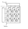
各光電変換素子は、放射線を可視光に変換する波長変換体と、可視光を受光して電気信号に変換する光電変換体とを有しており、波長変換体は、Gb2O3、Gb2O2S及びCsIのうちから選ばれた1種を母体材料として構成され、光電変換体は、アモルファスシリコンを主材料として構成されている。また、各光電変換素子を、放射線を吸収して前記波長変換体を介さず直接的に電気信号に変換する機能を有するように構成し、その主たる材料として、アモルファスセレン、ヒ素化ガリウム、ヨウ化水銀、ヨウ化鉛から選ばれた1種としてもよい。なお、ここでは記載の便宜上、3×3画素分の光電変換素子を例示したが、実際の構成では更に多数の光電変換素子が配列される。
【0034】
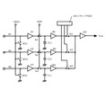
図2は、本実施形態の主要構成をなす図1の読み出し用回路107の内部構造を示す回路図である。
図2において、RES1〜RES3は読み出し回路に接続される入力配線M1〜M3をリセットするスイッチである。A1〜A3はM1〜M3の信号を増幅するアンプ、CL1〜CL3はA1〜A3で増幅された信号を一時的に記憶するサンプルホ−ルド容量、Sn1〜Sn3はサンプルホールドするためのスイッチ、B1〜B3はバッファアンプ、Sr1〜Sr3は並列信号を直列変換するためのスイッチ、103はスイッチSr1〜Sr3に直列変換するためのパルスを与えるシフトレジスタであり、スイッチSr1〜Sr3とシフトレジスタ103からアナログマルチプレクサが構成される。104は直列変換された信号を出力するバッファアンプである。
【0035】
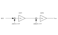
図3は、図1の読み出し用回路107の構成を単純化した回路モデルであり、アナログマルチプレクサを省略した回路図である。
アナログマルチプレクサより前段のアンプAMP1の入力換算ノイズ密度をNf(V/Hz1/2)、周波数帯域をBf(Hz)、ゲインをGf(倍)とし、マルチプレクサより後段のアンプAMP2の入力換算ノイズ密度をNb(V/Hz1/2)、周波数帯域をBb(Hz)、ゲインをGb(倍)とすると、前段のアンプでのノイズ量Vf(Vrms)、後段でのアンプのノイズ量Vb(Vrms)は、それぞれ、
Vf=Gf・(Nf2・Bf)1/2=Gf・N1 (Vrms)
Vb=Gb・(Nb2・Bb)1/2=Gb・N2 (Vrms)
となる。ここで、N1=(Nf2・Bf)1/2、N2=(Nb2・Bb)1/2である。
【0036】
これに対して、APM2では、前段のAMP1のノイズをGb(倍)されるため、出力における二つのノイズの総量Vout(noise)は、
Vout(noise)=[(Gb・Vf)2+Vb2]1/2
=[(Gb・Gf・N1)2+(Gb・N2)2]1/2
となる。
【0037】
一方、信号量Vout(signal)は、AMP1、AMP2でそれぞれGf(倍)、Gb(倍)されるために、
Vout(signal)=Gf・Gb・Vin(noise)
となる。従って、S/Nは、
S/N=Vout(signal)/Vout(noise)
=Vin(signal)/[N12+(N2/Gf)2]1/2
このことは、AMP1で設定されるゲインGfが大きいほど、S/Nが向上することを意味している。
【0038】
本実施形態では、アナログマルチプレクサの前段に配置されるアンプA1〜A3は、非反転増幅アンプが形成されており、フィードバック抵抗が制御信号GAINにより2つ並列接続されている。すなわち、制御信号GAINにより増幅率(ゲイン)が可変できるようになっている。一例として、A1に接続される三つの抵抗を全て同一の抵抗値とすれば、2倍と3倍とを切り替えることができる。抵抗の値を選ぶことにより、切り替えるゲインの種類をいかようにも設定することが可能である。
【0039】
図4は、本実施形態のX線撮像装置における動作タイミングを示す模式図である。
ここでは、動画撮影モードを50フレーム分行い、その後、静止画撮影モードを51フレーム目で行ったタイミング例を示している。紙面右へ進む方向が時間の経過を示している。また図2では、従来例の図6で示したタイミングチャートにおけるX線照射期間を「X」とし、読み取り期間を「R」としている。
【0040】
動画撮影モードでは、X線照射動作「X」と読み取り動作「R」を交互に繰り返している。この時、図1におけるアンプA1〜A3のゲインはGfに接続されており、Gfは、後の51フレーム目で行われる静止画撮影モードで設定されるGsより高い設定にされることが本実施形態の主要な特徴である。こうすることにより、動画撮影モードのS/Nは、同じ信号量(S)の場合、静止画撮影モードのS/Nよりも高くなるため、画質性能が向上する。
【0041】
なお、静止画撮影においても、アンプA1〜A3のゲインを高くするほどS/Nが向上することは動画撮影モードと同様である。しかしながら、静止画撮影モードでは動画撮影モードと違って1フレーム分だけのX線照射を行うため、より鮮明な画像を取得するためには、動画の1フレーム分の動作時よりも大きなX線量を照射する。通常A1〜A3、B1〜B3などの読み取り回路内のアンプが飽和しない程度のゲインが設定される。
【0042】
これに対して、動画撮影モードでは、連続的にX線を照射するため、患者への被爆線量を少しでも低減させるためには、1フレームあたりのX線量を下げなければならない。すなわち、動画撮影モードでの1フレームあたりのX線量は、静止画撮影モードの時よりも少ない。例えば動画撮影モードのX線量が静止画撮影モードの時の1/30であれば、動画撮影モードにおけるゲインGfは静止画撮影モードにおけるゲインGsの30倍高く設定することができる。
【0043】
図4においては、動画撮影モードから静止画撮影モードに遷移する動作タイミングで記載がなされている。これは、動画撮影モードで透視画像を医師がモニターしながら、静止画像を得たいタイミングで静止画撮影モードに遷移する。静止画に遷移するトリガー(命令)は医師から当該X線撮像装置側へ発生させる。また、透視中の動画像は、透視するだけではなく、記録媒体に記録してもよい。また、動画撮影モードから静止画撮影モードに遷移するのではなく、動画撮影モードを単独や静止画撮影モード単独で使用してもよい。
【0044】
図4では、動画撮影モードにおける読み取り動作において、X線照射動作「X」と光電変換回路の読み取り動作「R」を交互に繰り返す動作で説明したが、読み取り期間「R」の動作時間が一定であれば、X線照射は図4のようにパルス状に照射する必要はなく、点灯させ続けてもよい。そうすれば、動画撮影モードの読み取りサイクルが短くでき、動画のフレームレートを高くすることができる。
【0045】
また、図4では、動画撮影モードの読み取り動作「R」と静止画撮影モードの読み取り動作「R」を区別無く表記しているが、読み取り動作に必要な時間は同じであるとは限らない。動画撮影に必要な読み取り期間は、撮影部位により異なるが10m秒〜200m秒に対し、静止画像を撮影するのに必要な読み取り期間は、動画に比べて一般的には長く、100m秒〜1000m秒程度に設定される。これらは、スイッチ素子の性能、読み取り回路のアンプの性能などにより決定される。
【0046】
また、図1では、制御信号GAINにより、A1〜A3のゲインを2種類切り替えているが、これに限定されることなく、動画撮影モードにおけるX線量によっては、ゲイン切り替えを複数種類準備してもよい。この場合、図2においてアンプA1〜A3のフィードバック端子に抵抗とスイッチが更に付加され、ゲイン端子は1本ではなく、複数本準備される。
【0047】
また、図2では、アンプA1〜A3に、ゲインの切り替え機能を具備しているが、更にB1〜B3に切り替え機能を持たせてもよい。すなわち、本実施形態では、ゲインの切り替え機能を有するアンプの接続部位はアナログマルチプレクサの前段であればどこでもよい。
【0048】
以上説明したように、本実施形態のX線撮像装置によれば、動画撮影モードと静止画撮影モードとで読み取り回路内においてアナログマルチプレクサより前段のアンプA1〜A3のゲインを切り替える機能を持ち、動画撮影モードでは、静止画撮影モードより、高いゲインに設定することにより、動画撮影モードにおけるS/Nが向上する。更に、動画と静止画を同一の装置で撮影でき、例えばI.I.よりも小型な装置構成でフィルムと同等の画質性能を実現することができる。
【0049】
【発明の効果】
本発明の放射線撮像装置によれば、透視撮影を行なうに際して、動画撮影及び静止画撮影の双方を同一の装置で選択的に可能とし、かつI.I.に比して小型・軽量であり、フィルムに相当する静止画の画質性能を有する放射線撮像装置及び方法を提供することができる。
【図面の簡単な説明】
【図1】本実施形態によるアモルファスシリコン薄膜半導体を用いたX線撮像装置の概略構成を示す回路図である。
【図2】本実施形態の主要構成をなす読み出し用回路の内部構造を示す回路図である。
【図3】本実施形態の主要構成をなす読み出し用回路の構成を単純化した回路モデルであり、マルチプレクサを省略した回路図である。
【図4】本実施形態のX線撮像装置における動作タイミングを示す模式図である。
【図5】従来のX線撮像装置の読み出し用回路の内部構造を示す回路図である。
【図6】図5の読み出し用回路を備えたX線撮像装置の動作を示すタイムチャ−トである。
【符号の説明】
S1−1〜S3−3 光電変換素子
T1−1〜T3−3 スイッチング素子
101 光電変換回路
102 シフトレジスタ(スイッチング素子用)
103 シフトレジスタ(読み出しスイッチ用)
G1〜G3 ゲート駆動配線
M1〜M3 マトリクス信号配線
Vs 光電変換素子のバイアス線
107 読み出し用回路
CM1〜CM3 マトリクス信号配線に付加している読み出し容量
RES1〜RES3 CM1〜CM3をリセットするスイッチ
A1〜A3,B1〜B3,104 アンプ
Sn1〜Sn3 読み出し容量に信号を転送するための転送スイッチ
Sr1〜Sr3 読み出し容量の信号を順次読み出すための読み出し用スイッチ[0001]
TECHNICAL FIELD OF THE INVENTION
The present invention relates to a radiation imaging apparatus and method, and particularly to a radiation detection system used for diagnosis in a hospital and a radiation imaging apparatus also used as an industrial nondestructive inspection apparatus.
[0002]
[Prior art]
At present, in the medical X-ray still image photographing system, a film system in which a patient is irradiated with X-rays and a transmitted X-ray image is exposed on a film is mainly used. Films have a function of displaying and recording information, can have a large area, have high gradation, are lightweight, and are easy to handle. On the other hand, there are still problems such as the complexity of the development process, the problem of long-term storage location, and the time and labor required for searching.
[0003]
On the other hand, an image intensifier (II) is mainly used as a moving image capturing system. I. I. Is generally high in sensitivity and is excellent in terms of exposure dose because it utilizes the photomultiplier effect inside the device. On the other hand, it has been pointed out that there are disadvantages such as distortion of peripheral images due to the influence of the optical system, low contrast, and a large device. I. I. Not only can a doctor monitor a fluoroscopic image of a patient, but also the analog output of a CCD can be converted to digital and recorded, displayed, and stored. However, since high gradation is required for diagnosis, I.F. I. In many cases, a film is used in still image shooting even if is used.
[0004]
Recently, the demand for digitization of X-ray images in hospitals is increasing, and instead of film, X-ray detectors in which solid-state image sensors are arranged in a two-dimensional array are used to convert X-ray doses into electric signals. X-ray imaging devices have begun to be used. This is because X-ray images can be replaced with digital information, which makes it possible to transmit image information remotely and instantaneously. There is an advantage that can be. If film is not used, there is an advantage that the storage space of the film can be saved in the hospital. In the future, if excellent image processing technology can be introduced, the possibility of automatic diagnosis using a computer without the intervention of a radiologist is greatly expected.
[0005]
In recent years, a radiation imaging apparatus capable of capturing a still image using an amorphous silicon thin film semiconductor as a solid-state imaging device has been put to practical use. Using an amorphous silicon thin film semiconductor manufacturing technology, a large area exceeding 40 cm square covering the size of the human chest has been realized. Since the manufacturing process is relatively easy, it is expected to provide an inexpensive detection device in the future. In addition, since amorphous silicon can be made into a thin glass of 1 mm or less, there is an advantage that the thickness as a detector can be made very thin.
[0006]
Specifically, FIG. 5 shows an internal configuration of a readout circuit of an X-ray imaging device using an amorphous silicon thin film semiconductor for a solid-state imaging device.
In FIG. 5, RES1 to RES3 are switches for resetting M1 to M3, A1 to A3 are amplifiers for amplifying the signals of M1 to M3, and CL1 to CL3 are sample and hold for temporarily storing the signals amplified by A1 to A3. Capacitors, Sn1 to Sn3, switches for sample and hold, B1 to B3, buffer amplifiers, Sr1 to Sr3, switches for serial conversion of parallel signals, 103, a shift for giving a pulse for serial conversion to Sr1 to
[0007]
FIG. 6 is a time chart showing the operation of the X-ray imaging apparatus provided with the readout circuit of FIG.
First, the photoelectric conversion period (X-ray irradiation period) will be described.
When the light source (X-ray) is turned on in a pulsed manner in a state where all the TFTs are off, light is irradiated to each photoelectric conversion element, and signal charges corresponding to the amount of light are accumulated in the element capacitance. If a phosphor for X-ray to visible conversion is used, a member that guides visible light corresponding to the amount of X-rays to the photoelectric conversion element side is used, or the phosphor is disposed very close to the photoelectric conversion element. do it. Note that, even after the light source is turned off, the signal charge photoelectrically converted to the element capacitance is held.
[0008]
Next, a reading period will be described.
The read operation is performed in the order of the first row of S1-1 to S1-3, the second row of S2-1 to S2-3, and the third row of S3-1 to S3-3. First, in order to read the first row of S1-1 to S1-3, a gate pulse is applied from SR1 to the gate wiring G1 of the switch elements (TFT) T1-1 to T1-3. Thereby, T1-1 to T1-3 are turned on, and the signal charges stored in S1-1 to S1-3 are transferred to the signal wirings M1 to M3. Readout capacitances CM1 to CM3 (see FIG. 1) are added to the signal lines M1 to M3, and the signal charges are transferred to the readout capacitances CM1 to CM3 via TFTs. For example, the read capacitance CM1 to which the signal wiring M1 is added is equal to the sum of the capacitances (Cgs) between the gates and the sources of T1-1 to T3-1 (see FIG. 1) connected to M1. ). The signal charges transferred to M1 to M3 are amplified by amplifiers A1 to A3.
[0009]
The signals are transferred to the capacitors CL1 to CL3, and the SMPL signal is turned off and held. Next, by applying pulses from the shift register 103 in the order of the switches Sr1, Sr2, and Sr3, the signals held in CL1 to CL3 are output from the
[0010]
If the signals M1 to M3 are sampled and held at CL1 to CL3 by the SMPL signal of the first row, M1 to M3 can be reset to the GND potential by the CRES signal, and then the gate pulse of G2 can be applied. That is, while the signal of the first row is subjected to the serial conversion operation by SR2, the signal charges of the second row of the photoelectric conversion elements S2-1 to S2-3 can be simultaneously transferred by SR1.
Through the above operation, signal charges of the photoelectric conversion elements in all of the first to third rows can be output.
[0011]
[Problems to be solved by the invention]
I. I. When using as a moving image shooting, there is an advantage that the sensitivity is higher than a radiation imaging apparatus using amorphous silicon, but there are problems such as distortion of the peripheral image and low contrast, and when acquiring a still image, However, there is also a problem that the device becomes large, for example, a mechanism for inserting a film immediately before shooting is inserted.
[0012]
On the other hand, a radiation imaging apparatus using an amorphous silicon thin film semiconductor has been put to practical use at present, and the image quality performance as a still image is evaluated to be equal to or higher than that of a conventional film. However, it has not been put to practical use for shooting moving images for fluoroscopic purposes. One of the reasons is that since the exposure dose to the patient increases in moving image shooting, the X-ray dose during the moving image shooting period must be reduced as much as possible, and therefore, the signal amount is low and the S / N is poor. . Further, in moving image shooting, the scan speed (frame rate) often needs to be higher (faster) than in still image shooting, and in that case, the frequency band of the imaging device must be widened. This increases the so-called white noise such as shot noise and Johnson noise generated in the readout system of the solid-state imaging device, and has a problem of deteriorating the S / N in moving image shooting.
[0013]
In FIG. 5, the number of inputs is three and the number of outputs is one, and the analog multiplexer 103 (Sr1 to Sr3) converts a parallel signal into a serial signal. Usually, the amplifiers A1 and B1 are set to a frequency band in which a signal from the photoelectric conversion circuit can be amplified within the operation time for one line. Making the band wider than necessary is not preferable because it increases Johnson noise (thermal noise) generated in the amplifier. On the other hand, since an analog signal must be serially converted by an amplifier and a multiplexer (103, Sr1 to Sr3) subsequent to the analog multiplexer, the frequency band must be set wider than the frequency band of the A1 or A3 amplifier.
[0014]
Generally, Johnson noise (Vrms) is
Vrms = (4KTRB)1/2
Is represented by
Here, K is the Boltzmann constant, T is the absolute temperature, R is the resistance value, and B is the frequency band. B1/2Do not multiply (4KTR)1/2Is called a noise density.
[0015]
The operational amplifier generates Johnson noise from all the components, such as the on-resistance of the first-stage transistor constituting the amplifier and the input resistance and the feedback resistance (not shown in FIG. 5). Is proportional to
[0016]
For example, in FIG. 5, the
[0017]
In the case of chest X-ray imaging used in hospitals, it is said that a light receiving area having an area of 40 cm × 40 cm or more is required because the chest of a human body must be imaged. In this case, the pixel pitch is preferably at most 200 μm, and preferably less than 200 μm. For example, when 40 cm × 40 cm is manufactured at a pitch of 200 μm, the number of pixels needs to be 2000 pixels × 2000 pixels = 4,000,000 pixels. That is, the number of inputs in the readout circuit of FIG. 5 is 2000 pixels.
[0018]
It is not realistic to manufacture 2000 input wirings with a single readout circuit at 40 cm, and a design is usually made by dividing the readout circuits into a plurality of readout circuits. For example, when divided into ten readout circuits (ICs), the number of inputs is 200 and the number of outputs is one, which can be said to be realistic. In this case, the 104 amplifier requires 200 times the frequency band of the A1 amplifier. Assuming that the 104 amplifier and the A1 amplifier have the same noise density, the effective noise value of the 104 amplifier is 200 times higher.1/2The noise amount is multiplied by 14 times.
[0019]
SUMMARY OF THE INVENTION The present invention has been made in view of the above-mentioned problem, and has been made possible by selectively performing both moving image shooting and still image shooting with the same device when performing fluoroscopic shooting. I. It is an object of the present invention to provide a radiation imaging apparatus and method which are smaller and lighter in weight and have image quality performance of a still image equivalent to a film.
[0020]
[Means for Solving the Problems]
The radiation imaging apparatus according to the present invention includes: a radiation detection unit in which a plurality of radiation detection elements that convert radiation into electric signals are arranged in a matrix; a driving unit that drives and controls the radiation detection unit; A reading means for reading an electric signal, wherein a moving image shooting mode and a still image shooting mode can be selectively set; the reading means comprises a variable amplification means having a variable gain; and Control means for controlling the gain of the means, wherein the gain (Gf) in the moving image shooting mode is made larger than the gain (Gs) in the still image shooting mode by controlling the gain of the variable amplifying means by the control means. Set.
[0021]
In one aspect of the radiation imaging apparatus of the present invention, the readout unit includes a multiplexer that outputs a parallel signal from the radiation detection unit as a serial signal, and the variable amplification unit is provided at a stage preceding the multiplexer.
[0022]
In one aspect of the radiation imaging apparatus of the present invention, when capturing a still image, a moving image is acquired by a gain (Gf) set in advance in the moving image capturing mode, and a moving image is acquired in response to a signal requesting still image capturing. Then, the still image is acquired by switching to the gain (Gs) in the still image shooting mode.
[0023]
In one aspect of the radiation imaging apparatus of the present invention, a fixed amplification unit having a fixed gain is provided at a stage subsequent to the multiplexer.
[0024]
In one aspect of the radiation imaging apparatus of the present invention, the radiation detection element has a wavelength converter that converts radiation into visible light, and a photoelectric converter that receives visible light and converts it into an electric signal.
[0025]
In one aspect of the radiation imaging apparatus of the present invention, the wavelength converter is a Gb2O3, Gb2O2One selected from S and CsI is configured as a base material.
[0026]
In one aspect of the radiation imaging apparatus of the present invention, the photoelectric conversion body is configured using amorphous silicon as a main material.
[0027]
In one aspect of the radiation imaging apparatus of the present invention, the radiation detection element has a switch element.
[0028]
In one aspect of the radiation imaging apparatus of the present invention, the radiation detection element has a function of absorbing radiation and directly converting it to an electric signal without passing through the wavelength converter, and its main materials are amorphous selenium and arsenic. One type selected from gallium iodide, mercury iodide, and lead iodide
[0029]
The radiation imaging method according to the present invention is a radiation imaging apparatus in which a plurality of radiation detection elements for converting radiation into electric signals are arranged in a matrix, and a moving image shooting mode and a still image shooting mode can be selectively set. Is used to make the gain variable, and the gain control sets the gain (Gf) in the moving image shooting mode to be larger than the gain (Gs) in the still image shooting mode.
[0030]
According to one aspect of the radiation imaging method of the present invention, when capturing a still image, a moving image is acquired with a gain (Gf) set in advance in the moving image capturing mode, and a moving image is acquired in response to a signal requesting still image capturing. Then, the still image is acquired by switching to the gain (Gs) in the still image shooting mode.
[0031]
BEST MODE FOR CARRYING OUT THE INVENTION
Hereinafter, preferred embodiments to which the present invention is applied will be described in detail with reference to the drawings.
FIG. 1 is a schematic configuration of an X-ray imaging device using an amorphous silicon thin film semiconductor according to the present embodiment, and is a plan circuit diagram of an X-ray imaging device using a photoelectric conversion element that captures visible light and converts it into an electric signal. is there. In this X-ray imaging apparatus, a moving image shooting mode and a still image shooting mode can be selectively set. FIG. 1 does not show a phosphor that converts X-rays into visible light. In the present embodiment, X-ray imaging is exemplified, but the present invention is not limited to this, and will be described as including α-rays, β-rays, γ-rays, and the like in the category of radiation.
[0032]
In FIG. 1, S1-1 to S3-3 are photoelectric conversion elements arranged in a matrix, T1-1 to T3-3 are switch elements (TFTs), and G1 to G3 are gate wirings for turning on / off the TFTs. , M1 to M3 are signal wirings. In the photoelectric conversion element, a photodiode and a capacitor are represented in parallel connection, and a reverse bias is applied. That is, the cathode side of the photodiode is biased to + (plus). The bias wiring is usually a common wiring, but is omitted as a common wiring in FIG. The photoelectrically converted charge is stored in the capacitor. S1-1 to S3-3, T1-1 to T3-3, G1 to G3, M1 to M3, Vs line, and these are collectively referred to as a radiation detection circuit or a photoelectric conversion circuit. A shift register 102 applies a pulse to the gate lines G1 to G3 to drive and control the photoelectric conversion elements S1-1 to S3-3, and 107 amplifies parallel signal outputs of M1 to M3 in the photoelectric
[0033]
Each photoelectric conversion element has a wavelength converter that converts radiation into visible light, and a photoelectric converter that receives visible light and converts it into an electric signal.2O3, Gb2O2One selected from S and CsI is configured as a base material, and the photoelectric conversion body is configured using amorphous silicon as a main material. In addition, each photoelectric conversion element is configured to have a function of absorbing radiation and directly converting it to an electric signal without passing through the wavelength converter, and its main materials include amorphous selenium, gallium arsenide, and iodide. It may be one selected from mercury and lead iodide. Here, for convenience of description, a photoelectric conversion element for 3 × 3 pixels is illustrated, but in an actual configuration, a larger number of photoelectric conversion elements are arranged.
[0034]
FIG. 2 is a circuit diagram showing the internal structure of the
In FIG. 2, RES1 to RES3 are switches for resetting input wirings M1 to M3 connected to the readout circuit. A1 to A3 are amplifiers for amplifying the signals of M1 to M3, CL1 to CL3 are sample hold capacitors for temporarily storing the signals amplified by A1 to A3, Sn1 to Sn3 are switches for holding the sample, B1 B3 to S3 are buffer amplifiers, Sr1 to Sr3 are switches for converting serial signals into serial signals, 103 is a shift register that applies a pulse for converting the serial signals to the switches Sr1 to Sr3. A multiplexer is configured.
[0035]
FIG. 3 is a circuit model in which the configuration of the
The input-converted noise density of the amplifier AMP1 preceding the analog multiplexer is Nf (V / Hz).1/2), The frequency band is Bf (Hz), the gain is Gf (times), and the input converted noise density of the amplifier AMP2 downstream of the multiplexer is Nb (V / Hz).1/2), The frequency band is Bb (Hz), and the gain is Gb (times), the noise amount Vf (Vrms) of the preceding amplifier and the noise amount Vb (Vrms) of the following amplifier are respectively
Vf = Gf · (Nf2・ Bf)1/2= Gf · N1 (Vrms)
Vb = Gb · (Nb2・ Bb)1/2= Gb · N2 (Vrms)
It becomes. Here, N1 = (Nf2・ Bf)1/2, N2 = (Nb2・ Bb)1/2It is.
[0036]
On the other hand, in the APM2, the noise of the preceding AMP1 is Gb (multiplied), so that the total amount Vout (noise) of the two noises in the output is:
Vout (noise) = [(Gb · Vf)2+ Vb2]1/2
= [(Gb · Gf · N1)2+ (Gb · N2)2]1/2
It becomes.
[0037]
On the other hand, the signal amount Vout (signal) is Gf (multiplied) and Gb (multiplied) by AMP1 and AMP2, respectively.
Vout (signal) = Gf · Gb · Vin (noise)
It becomes. Therefore, S / N is
S / N = Vout (signal) / Vout (noise)
= Vin (signal) / [N12+ (N2 / Gf)2]1/2
This means that as the gain Gf set by AMP1 is larger, the S / N is improved.
[0038]
In the present embodiment, the amplifiers A1 to A3 arranged at the preceding stage of the analog multiplexer form a non-inverting amplification amplifier, and two feedback resistors are connected in parallel by the control signal GAIN. That is, the amplification rate (gain) can be varied by the control signal GAIN. As an example, if all three resistors connected to A1 have the same resistance value, switching between double and triple can be performed. By selecting the value of the resistor, the type of gain to be switched can be set in any manner.
[0039]
FIG. 4 is a schematic diagram illustrating operation timing in the X-ray imaging apparatus according to the present embodiment.
Here, a timing example is shown in which the moving image shooting mode is performed for 50 frames and then the still image shooting mode is performed for the 51st frame. The direction to the right on the paper indicates the passage of time. In FIG. 2, the X-ray irradiation period in the timing chart shown in FIG. 6 of the conventional example is “X”, and the reading period is “R”.
[0040]
In the moving image shooting mode, the X-ray irradiation operation “X” and the reading operation “R” are alternately repeated. At this time, the gains of the amplifiers A1 to A3 in FIG. 1 are connected to Gf, and Gf is set to be higher than Gs set in the still image shooting mode performed in the subsequent 51st frame. It is the main feature of the form. By doing so, the S / N in the moving image shooting mode is higher than the S / N in the still image shooting mode when the signal amount (S) is the same, so that the image quality performance is improved.
[0041]
It should be noted that in still image shooting, the higher the gain of the amplifiers A1 to A3, the higher the S / N ratio, as in the moving image shooting mode. However, in the still image shooting mode, unlike in the moving image shooting mode, only one frame of X-ray irradiation is performed. Therefore, in order to obtain a clearer image, a larger X-ray dose than in the operation of one moving image frame is required. Irradiate. Usually, gains such as A1 to A3 and B1 to B3 are set so that the amplifiers in the reading circuit are not saturated.
[0042]
On the other hand, in the moving image shooting mode, since the X-ray is continuously emitted, the X-ray dose per frame must be reduced in order to reduce the exposure dose to the patient as much as possible. That is, the X-ray dose per frame in the moving image shooting mode is smaller than that in the still image shooting mode. For example, if the X-ray dose in the moving image shooting mode is 1/30 of that in the still image shooting mode, the gain Gf in the moving image shooting mode can be set to be 30 times higher than the gain Gs in the still image shooting mode.
[0043]
In FIG. 4, the description is made at the operation timing of transition from the moving image shooting mode to the still image shooting mode. In this case, while the doctor monitors the fluoroscopic image in the moving image shooting mode, the mode shifts to the still image shooting mode at a timing when a still image is desired to be obtained. A trigger (command) for transitioning to a still image is generated from the doctor to the X-ray imaging apparatus. In addition, a moving image during fluoroscopy may be recorded on a recording medium in addition to fluoroscopy. Instead of transitioning from the moving image shooting mode to the still image shooting mode, the moving image shooting mode may be used alone or in the still image shooting mode alone.
[0044]
In FIG. 4, in the reading operation in the moving image shooting mode, the X-ray irradiating operation “X” and the reading operation “R” of the photoelectric conversion circuit are alternately repeated, but the operation time of the reading period “R” is constant. If so, the X-ray irradiation need not be performed in a pulsed manner as shown in FIG. Then, the reading cycle in the moving image shooting mode can be shortened, and the frame rate of the moving image can be increased.
[0045]
In FIG. 4, the reading operation “R” in the moving image shooting mode and the reading operation “R” in the still image shooting mode are shown without distinction, but the time required for the reading operation is not necessarily the same. The reading period required for shooting a moving image varies depending on the imaging site, but the reading period required for shooting a still image is generally longer than that for a moving image, from 10 ms to 200 ms, and is 100 ms to 1000 ms. Set to about. These are determined by the performance of the switch element, the performance of the amplifier of the reading circuit, and the like.
[0046]
In FIG. 1, two types of gains A1 to A3 are switched by the control signal GAIN. However, the present invention is not limited to this. Depending on the X-ray dose in the moving image shooting mode, a plurality of types of gain switching may be prepared. Good. In this case, a resistor and a switch are further added to the feedback terminals of the amplifiers A1 to A3 in FIG. 2, and a plurality of gain terminals are prepared instead of one.
[0047]
Further, in FIG. 2, the amplifiers A1 to A3 have a gain switching function, but B1 to B3 may further have a switching function. That is, in the present embodiment, the connection part of the amplifier having the function of switching the gain may be any part as long as it is in front of the analog multiplexer.
[0048]
As described above, the X-ray imaging apparatus according to the present embodiment has a function of switching the gain of the amplifiers A1 to A3 preceding the analog multiplexer in the reading circuit between the moving image shooting mode and the still image shooting mode. In the shooting mode, the S / N in the moving image shooting mode is improved by setting a higher gain than in the still image shooting mode. Furthermore, moving images and still images can be shot by the same device. I. Image quality performance equivalent to that of a film can be realized with a smaller device configuration.
[0049]
【The invention's effect】
According to the radiation imaging apparatus of the present invention, when performing fluoroscopic imaging, both moving image imaging and still image imaging can be selectively enabled by the same apparatus. I. It is possible to provide a radiation imaging apparatus and a method which are smaller and lighter in weight and have a still image quality performance equivalent to a film.
[Brief description of the drawings]
FIG. 1 is a circuit diagram showing a schematic configuration of an X-ray imaging apparatus using an amorphous silicon thin film semiconductor according to the present embodiment.
FIG. 2 is a circuit diagram showing an internal structure of a readout circuit which is a main component of the present embodiment.
FIG. 3 is a simplified circuit model of a configuration of a readout circuit which is a main configuration of the embodiment, and is a circuit diagram in which a multiplexer is omitted.
FIG. 4 is a schematic diagram showing operation timing in the X-ray imaging apparatus of the embodiment.
FIG. 5 is a circuit diagram showing an internal structure of a readout circuit of a conventional X-ray imaging apparatus.
FIG. 6 is a time chart showing the operation of the X-ray imaging apparatus provided with the readout circuit of FIG.
[Explanation of symbols]
S1-1 to S3-3 photoelectric conversion element
T1-1 to T3-3 switching elements
101 photoelectric conversion circuit
102 shift register (for switching element)
103 shift register (for read switch)
G1 to G3 gate drive wiring
M1-M3 matrix signal wiring
Vs バ イ ア ス bias line of photoelectric conversion element
107 ° readout circuit
CM1 to CM3 Readout capacity added to matrix signal wiring
RES1 to RES3 @Switch for resetting CM1 to CM3
A1-A3, B1-B3, 104 amplifier
Transfer switches for transferring signals to Sn1 to Sn3 readout capacitors
Read switch for sequentially reading signals of Sr1 to Sr3rread capacity
Claims (11)
前記放射線検出手段を駆動制御する駆動手段と、
前記放射線検出手段からの電気信号を読み出すための読み出し手段と
を含み、
動画撮影モードと静止画撮影モードとを選択的に設定自在とされており、
前記読み出し手段は、ゲインが可変とされた可変増幅手段と、前記増幅手段のゲインを制御する制御手段とを備え、
前記制御手段による前記可変増幅手段のゲイン制御により、前記動画撮影モード時のゲイン(Gf)を前記静止画撮影モード時のゲイン(Gs)よりも大きく設定することを特徴とする放射線撮像装置。Radiation detection means in which a plurality of radiation detection elements that convert radiation into electrical signals are arranged in a matrix,
Driving means for driving and controlling the radiation detection means,
A readout unit for reading out an electric signal from the radiation detection unit,
The video shooting mode and the still image shooting mode can be set selectively.
The readout unit includes a variable amplification unit having a variable gain, and a control unit that controls a gain of the amplification unit,
A radiation imaging apparatus, wherein the gain (Gf) in the moving image shooting mode is set to be larger than the gain (Gs) in the still image shooting mode by gain control of the variable amplifying unit by the control unit.
前記可変増幅手段が前記マルチプレクサよりも前段に設けられていることを特徴とする請求項1に記載の放射線撮像装置。The reading unit includes a multiplexer that outputs a parallel signal from the radiation detection unit as a serial signal,
The radiation imaging apparatus according to claim 1, wherein the variable amplification unit is provided at a stage before the multiplexer.
ゲインを可変とし、当該ゲイン制御により、前記動画撮影モード時のゲイン(Gf)を前記静止画撮影モード時のゲイン(Gs)よりも大きく設定することを特徴とする放射線検出方法。A plurality of radiation detection elements that convert radiation into electrical signals are arranged in a matrix, using a radiation imaging apparatus that is capable of selectively setting a moving image shooting mode and a still image shooting mode,
A radiation detection method, wherein a gain is variable, and a gain (Gf) in the moving image shooting mode is set to be larger than a gain (Gs) in the still image shooting mode by the gain control.
Priority Applications (2)
| Application Number | Priority Date | Filing Date | Title |
|---|---|---|---|
| JP2002178800A JP2004023654A (en) | 2002-06-19 | 2002-06-19 | Radiographic device and radiographic method |
| US10/464,012 US7075090B2 (en) | 2002-06-19 | 2003-06-18 | Radiological imaging apparatus and radiological imaging method |
Applications Claiming Priority (1)
| Application Number | Priority Date | Filing Date | Title |
|---|---|---|---|
| JP2002178800A JP2004023654A (en) | 2002-06-19 | 2002-06-19 | Radiographic device and radiographic method |
Publications (2)
| Publication Number | Publication Date |
|---|---|
| JP2004023654A true JP2004023654A (en) | 2004-01-22 |
| JP2004023654A5 JP2004023654A5 (en) | 2007-08-16 |
Family
ID=30112236
Family Applications (1)
| Application Number | Title | Priority Date | Filing Date |
|---|---|---|---|
| JP2002178800A Pending JP2004023654A (en) | 2002-06-19 | 2002-06-19 | Radiographic device and radiographic method |
Country Status (2)
| Country | Link |
|---|---|
| US (1) | US7075090B2 (en) |
| JP (1) | JP2004023654A (en) |
Cited By (5)
| Publication number | Priority date | Publication date | Assignee | Title |
|---|---|---|---|---|
| WO2006013975A1 (en) * | 2004-08-06 | 2006-02-09 | Canon Kabushiki Kaisha | Imaging apparatus, imaging system, imaging method, and computer program |
| JP2009297078A (en) * | 2008-06-10 | 2009-12-24 | Canon Inc | Radiography control apparatus and radiography control method |
| KR20100135705A (en) * | 2008-04-24 | 2010-12-27 | 하마마츠 포토닉스 가부시키가이샤 | Solid-state image pickup apparatus and x-ray inspection system |
| JP2012182836A (en) * | 2012-05-28 | 2012-09-20 | Hamamatsu Photonics Kk | X-ray inspection system |
| JP2012257172A (en) * | 2011-06-10 | 2012-12-27 | Canon Inc | Imaging apparatus and imaging element |
Families Citing this family (5)
| Publication number | Priority date | Publication date | Assignee | Title |
|---|---|---|---|---|
| JP4290066B2 (en) * | 2004-05-20 | 2009-07-01 | キヤノン株式会社 | Solid-state imaging device and imaging system |
| JP5317388B2 (en) * | 2005-09-30 | 2013-10-16 | キヤノン株式会社 | Radiation imaging apparatus, radiation imaging system, and program |
| FR2938936B1 (en) * | 2008-11-25 | 2016-01-15 | Sopro | MULTIFUNCTION IMAGE ACQUISITION DEVICE |
| JP2010160311A (en) * | 2009-01-08 | 2010-07-22 | Panasonic Corp | Imaging apparatus |
| EP3764127A1 (en) * | 2019-07-08 | 2021-01-13 | Siemens Healthcare GmbH | X-ray detector and x-ray apparatus with x-ray detector |
Family Cites Families (4)
| Publication number | Priority date | Publication date | Assignee | Title |
|---|---|---|---|---|
| US6163029A (en) | 1997-09-22 | 2000-12-19 | Kabushiki Kaisha Toshiba | Radiation detector, radiation detecting method and X-ray diagnosing apparatus with same radiation detector |
| JPH11331703A (en) * | 1998-03-20 | 1999-11-30 | Toshiba Corp | Image-pickup device |
| US6904126B2 (en) * | 2002-06-19 | 2005-06-07 | Canon Kabushiki Kaisha | Radiological imaging apparatus and method |
| JP4050117B2 (en) * | 2002-09-17 | 2008-02-20 | 富士フイルム株式会社 | Image information recording and reading method and apparatus |
-
2002
- 2002-06-19 JP JP2002178800A patent/JP2004023654A/en active Pending
-
2003
- 2003-06-18 US US10/464,012 patent/US7075090B2/en not_active Expired - Lifetime
Cited By (11)
| Publication number | Priority date | Publication date | Assignee | Title |
|---|---|---|---|---|
| WO2006013975A1 (en) * | 2004-08-06 | 2006-02-09 | Canon Kabushiki Kaisha | Imaging apparatus, imaging system, imaging method, and computer program |
| JP2006068512A (en) * | 2004-08-06 | 2006-03-16 | Canon Inc | Imaging apparatus, imaging system, imaging method, and computer program |
| US7532706B2 (en) | 2004-08-06 | 2009-05-12 | Canon Kabushiki Kaisha | Imaging apparatus, imaging system, imaging method, and computer program |
| KR20100135705A (en) * | 2008-04-24 | 2010-12-27 | 하마마츠 포토닉스 가부시키가이샤 | Solid-state image pickup apparatus and x-ray inspection system |
| US8576984B2 (en) | 2008-04-24 | 2013-11-05 | Hamamatsu Photonics K.K. | Solid-state image pickup apparatus and X-ray inspection system |
| US8953745B2 (en) | 2008-04-24 | 2015-02-10 | Hamamatsu Photonics K.K. | Solid-state image pickup apparatus and X-ray inspection system |
| KR101598233B1 (en) * | 2008-04-24 | 2016-02-26 | 하마마츠 포토닉스 가부시키가이샤 | Solid-state image pickup apparatus and x-ray inspection system |
| JP2009297078A (en) * | 2008-06-10 | 2009-12-24 | Canon Inc | Radiography control apparatus and radiography control method |
| US8737569B2 (en) | 2008-06-10 | 2014-05-27 | Canon Kabushiki Kaisha | Radiography control apparatus and radiography control method |
| JP2012257172A (en) * | 2011-06-10 | 2012-12-27 | Canon Inc | Imaging apparatus and imaging element |
| JP2012182836A (en) * | 2012-05-28 | 2012-09-20 | Hamamatsu Photonics Kk | X-ray inspection system |
Also Published As
| Publication number | Publication date |
|---|---|
| US7075090B2 (en) | 2006-07-11 |
| US20040008813A1 (en) | 2004-01-15 |
Similar Documents
| Publication | Publication Date | Title |
|---|---|---|
| US8809795B2 (en) | Imaging apparatus, radiation imaging system, controlling method of imaging apparatus, and recording medium recording control program of imaging apparatus | |
| US7421063B2 (en) | Radiation imaging apparatus, radiation imaging system, and method of controlling radiation imaging apparatus | |
| US7113565B2 (en) | Radiological imaging apparatus and method | |
| JP4469638B2 (en) | Reading device and image photographing device | |
| JP5389069B2 (en) | Radiation imaging apparatus, method thereof, and program | |
| US8482644B2 (en) | Solid-state imaging device | |
| US7302039B2 (en) | Radiography apparatus, radiography system, and control method thereof | |
| US20070040099A1 (en) | Radiation image pickup apparatus, radiation image pickup system, their control method and their control program | |
| US7078701B2 (en) | Radiographic apparatus and radiographic system | |
| JP2009121848A (en) | Radiation imaging apparatus, its drive method, and program | |
| JP4738954B2 (en) | Radiation imaging apparatus, method thereof, and program | |
| WO2007037121A1 (en) | Radiographic imaging apparatus and imaging method for radiographic imaging apparatus | |
| JP4383899B2 (en) | Radiation imaging apparatus and radiation imaging system | |
| JP4739060B2 (en) | Radiation imaging apparatus, radiation imaging system, and control method thereof | |
| JP2023134775A (en) | Radiography apparatus and radiography system | |
| JP2004023654A (en) | Radiographic device and radiographic method | |
| JP4314073B2 (en) | Radiation imaging apparatus and radiation imaging method | |
| WO2019049456A1 (en) | Radiation imaging apparatus, method for controlling same, and radiation imaging system | |
| JPWO2006112320A1 (en) | X-ray flat panel detector and X-ray diagnostic imaging apparatus | |
| JP2007221453A (en) | Radiation imager and its driving method | |
| JP5120458B2 (en) | Light or radiation imaging device | |
| JP4812503B2 (en) | X-ray equipment | |
| JP2006198416A (en) | Radiation image pickup system | |
| JP2018021828A (en) | Radiation imaging apparatus and radiation imaging system | |
| JP2002253541A (en) | Radiation detecting system |
Legal Events
| Date | Code | Title | Description |
|---|---|---|---|
| A521 | Request for written amendment filed |
Free format text: JAPANESE INTERMEDIATE CODE: A523 Effective date: 20050610 |
|
| A621 | Written request for application examination |
Free format text: JAPANESE INTERMEDIATE CODE: A621 Effective date: 20050610 |
|
| A521 | Request for written amendment filed |
Free format text: JAPANESE INTERMEDIATE CODE: A523 Effective date: 20070704 |
|
| A977 | Report on retrieval |
Free format text: JAPANESE INTERMEDIATE CODE: A971007 Effective date: 20080514 |
|
| A131 | Notification of reasons for refusal |
Free format text: JAPANESE INTERMEDIATE CODE: A131 Effective date: 20080527 |
|
| A521 | Request for written amendment filed |
Free format text: JAPANESE INTERMEDIATE CODE: A523 Effective date: 20080728 |
|
| A02 | Decision of refusal |
Free format text: JAPANESE INTERMEDIATE CODE: A02 Effective date: 20090602 |