EP3763720B1 - Compound and organic light emitting device comprising same - Google Patents
Compound and organic light emitting device comprising same Download PDFInfo
- Publication number
- EP3763720B1 EP3763720B1 EP19793229.6A EP19793229A EP3763720B1 EP 3763720 B1 EP3763720 B1 EP 3763720B1 EP 19793229 A EP19793229 A EP 19793229A EP 3763720 B1 EP3763720 B1 EP 3763720B1
- Authority
- EP
- European Patent Office
- Prior art keywords
- compound
- layer
- preparation
- chemical formula
- group
- Prior art date
- Legal status (The legal status is an assumption and is not a legal conclusion. Google has not performed a legal analysis and makes no representation as to the accuracy of the status listed.)
- Active
Links
- 150000001875 compounds Chemical class 0.000 title claims description 602
- 125000003118 aryl group Chemical group 0.000 claims description 91
- 239000000126 substance Substances 0.000 claims description 84
- 238000002347 injection Methods 0.000 claims description 69
- 239000007924 injection Substances 0.000 claims description 69
- 125000004432 carbon atom Chemical group C* 0.000 claims description 47
- 229910052739 hydrogen Inorganic materials 0.000 claims description 42
- 239000001257 hydrogen Substances 0.000 claims description 42
- 239000011368 organic material Substances 0.000 claims description 42
- 125000001072 heteroaryl group Chemical group 0.000 claims description 41
- 230000027756 respiratory electron transport chain Effects 0.000 claims description 36
- JYEUMXHLPRZUAT-UHFFFAOYSA-N 1,2,3-triazine Chemical compound C1=CN=NN=C1 JYEUMXHLPRZUAT-UHFFFAOYSA-N 0.000 claims description 32
- UFHFLCQGNIYNRP-UHFFFAOYSA-N Hydrogen Chemical compound [H][H] UFHFLCQGNIYNRP-UHFFFAOYSA-N 0.000 claims description 31
- YZCKVEUIGOORGS-OUBTZVSYSA-N Deuterium Chemical compound [2H] YZCKVEUIGOORGS-OUBTZVSYSA-N 0.000 claims description 13
- 229910052805 deuterium Inorganic materials 0.000 claims description 13
- 125000000217 alkyl group Chemical group 0.000 claims description 12
- 150000002431 hydrogen Chemical class 0.000 claims description 11
- 239000002019 doping agent Substances 0.000 claims description 8
- 239000010410 layer Substances 0.000 description 250
- 238000002360 preparation method Methods 0.000 description 213
- 238000000034 method Methods 0.000 description 104
- YXFVVABEGXRONW-UHFFFAOYSA-N Toluene Chemical compound CC1=CC=CC=C1 YXFVVABEGXRONW-UHFFFAOYSA-N 0.000 description 75
- ZMXDDKWLCZADIW-UHFFFAOYSA-N N,N-Dimethylformamide Chemical compound CN(C)C=O ZMXDDKWLCZADIW-UHFFFAOYSA-N 0.000 description 60
- LFQSCWFLJHTTHZ-UHFFFAOYSA-N Ethanol Chemical compound CCO LFQSCWFLJHTTHZ-UHFFFAOYSA-N 0.000 description 56
- HEDRZPFGACZZDS-UHFFFAOYSA-N Chloroform Chemical compound ClC(Cl)Cl HEDRZPFGACZZDS-UHFFFAOYSA-N 0.000 description 54
- WYURNTSHIVDZCO-UHFFFAOYSA-N Tetrahydrofuran Chemical compound C1CCOC1 WYURNTSHIVDZCO-UHFFFAOYSA-N 0.000 description 50
- 239000000203 mixture Substances 0.000 description 46
- XEKOWRVHYACXOJ-UHFFFAOYSA-N Ethyl acetate Chemical compound CCOC(C)=O XEKOWRVHYACXOJ-UHFFFAOYSA-N 0.000 description 45
- CDBYLPFSWZWCQE-UHFFFAOYSA-L Sodium Carbonate Chemical compound [Na+].[Na+].[O-]C([O-])=O CDBYLPFSWZWCQE-UHFFFAOYSA-L 0.000 description 44
- NFHFRUOZVGFOOS-UHFFFAOYSA-N palladium;triphenylphosphane Chemical compound [Pd].C1=CC=CC=C1P(C=1C=CC=CC=1)C1=CC=CC=C1.C1=CC=CC=C1P(C=1C=CC=CC=1)C1=CC=CC=C1.C1=CC=CC=C1P(C=1C=CC=CC=1)C1=CC=CC=C1.C1=CC=CC=C1P(C=1C=CC=CC=1)C1=CC=CC=C1 NFHFRUOZVGFOOS-UHFFFAOYSA-N 0.000 description 39
- 239000000463 material Substances 0.000 description 38
- HXITXNWTGFUOAU-UHFFFAOYSA-N phenylboronic acid Chemical compound OB(O)C1=CC=CC=C1 HXITXNWTGFUOAU-UHFFFAOYSA-N 0.000 description 32
- -1 acenaphthyl group Chemical group 0.000 description 29
- CSNNHWWHGAXBCP-UHFFFAOYSA-L Magnesium sulfate Chemical compound [Mg+2].[O-][S+2]([O-])([O-])[O-] CSNNHWWHGAXBCP-UHFFFAOYSA-L 0.000 description 28
- YLQBMQCUIZJEEH-UHFFFAOYSA-N Furan Chemical compound C=1C=COC=1 YLQBMQCUIZJEEH-UHFFFAOYSA-N 0.000 description 27
- 239000000243 solution Substances 0.000 description 24
- BWHMMNNQKKPAPP-UHFFFAOYSA-L potassium carbonate Chemical compound [K+].[K+].[O-]C([O-])=O BWHMMNNQKKPAPP-UHFFFAOYSA-L 0.000 description 23
- 229910000029 sodium carbonate Inorganic materials 0.000 description 22
- XLYOFNOQVPJJNP-UHFFFAOYSA-N water Substances O XLYOFNOQVPJJNP-UHFFFAOYSA-N 0.000 description 22
- 230000000052 comparative effect Effects 0.000 description 20
- 229940126214 compound 3 Drugs 0.000 description 15
- 238000000151 deposition Methods 0.000 description 13
- 229910052943 magnesium sulfate Inorganic materials 0.000 description 13
- 239000000758 substrate Substances 0.000 description 13
- 239000000706 filtrate Substances 0.000 description 12
- 235000019341 magnesium sulphate Nutrition 0.000 description 12
- 125000001997 phenyl group Chemical group [H]C1=C([H])C([H])=C(*)C([H])=C1[H] 0.000 description 11
- AMEVJOWOWQPPJQ-UHFFFAOYSA-N 2,4-dichloro-6-phenyl-1,3,5-triazine Chemical compound ClC1=NC(Cl)=NC(C=2C=CC=CC=2)=N1 AMEVJOWOWQPPJQ-UHFFFAOYSA-N 0.000 description 10
- 229910000027 potassium carbonate Inorganic materials 0.000 description 10
- NSGDYZCDUPSTQT-UHFFFAOYSA-N N-[5-bromo-1-[(4-fluorophenyl)methyl]-4-methyl-2-oxopyridin-3-yl]cycloheptanecarboxamide Chemical compound Cc1c(Br)cn(Cc2ccc(F)cc2)c(=O)c1NC(=O)C1CCCCCC1 NSGDYZCDUPSTQT-UHFFFAOYSA-N 0.000 description 9
- 229940125904 compound 1 Drugs 0.000 description 9
- HSMOLGUTOVPFAI-UHFFFAOYSA-N 1,3-dibromo-4-chloro-2-nitrobenzene Chemical compound BrC1=C(C(=C(C=C1)Cl)Br)[N+](=O)[O-] HSMOLGUTOVPFAI-UHFFFAOYSA-N 0.000 description 8
- 229910052782 aluminium Inorganic materials 0.000 description 8
- XAGFODPZIPBFFR-UHFFFAOYSA-N aluminium Chemical compound [Al] XAGFODPZIPBFFR-UHFFFAOYSA-N 0.000 description 8
- SFHYNDMGZXWXBU-LIMNOBDPSA-N 6-amino-2-[[(e)-(3-formylphenyl)methylideneamino]carbamoylamino]-1,3-dioxobenzo[de]isoquinoline-5,8-disulfonic acid Chemical compound O=C1C(C2=3)=CC(S(O)(=O)=O)=CC=3C(N)=C(S(O)(=O)=O)C=C2C(=O)N1NC(=O)N\N=C\C1=CC=CC(C=O)=C1 SFHYNDMGZXWXBU-LIMNOBDPSA-N 0.000 description 7
- 150000004982 aromatic amines Chemical class 0.000 description 7
- 229910052751 metal Inorganic materials 0.000 description 7
- 239000002184 metal Substances 0.000 description 7
- UOXJNGFFPMOZDM-UHFFFAOYSA-N 2-[di(propan-2-yl)amino]ethylsulfanyl-methylphosphinic acid Chemical compound CC(C)N(C(C)C)CCSP(C)(O)=O UOXJNGFFPMOZDM-UHFFFAOYSA-N 0.000 description 6
- RAXXELZNTBOGNW-UHFFFAOYSA-N imidazole Natural products C1=CNC=N1 RAXXELZNTBOGNW-UHFFFAOYSA-N 0.000 description 6
- 125000001424 substituent group Chemical group 0.000 description 6
- SFUIGUOONHIVLG-UHFFFAOYSA-N (2-nitrophenyl)boronic acid Chemical compound OB(O)C1=CC=CC=C1[N+]([O-])=O SFUIGUOONHIVLG-UHFFFAOYSA-N 0.000 description 5
- 125000006267 biphenyl group Chemical group 0.000 description 5
- 239000010406 cathode material Substances 0.000 description 5
- 239000012153 distilled water Substances 0.000 description 5
- 230000000694 effects Effects 0.000 description 5
- QCSLIRFWJPOENV-UHFFFAOYSA-N (2-fluorophenyl)boronic acid Chemical compound OB(O)C1=CC=CC=C1F QCSLIRFWJPOENV-UHFFFAOYSA-N 0.000 description 4
- UZKBSZSTDQSMDR-UHFFFAOYSA-N 1-[(4-chlorophenyl)-phenylmethyl]piperazine Chemical compound C1=CC(Cl)=CC=C1C(C=1C=CC=CC=1)N1CCNCC1 UZKBSZSTDQSMDR-UHFFFAOYSA-N 0.000 description 4
- HTFNVAVTYILUCF-UHFFFAOYSA-N 2-[2-ethoxy-4-[4-(4-methylpiperazin-1-yl)piperidine-1-carbonyl]anilino]-5-methyl-11-methylsulfonylpyrimido[4,5-b][1,4]benzodiazepin-6-one Chemical compound CCOc1cc(ccc1Nc1ncc2N(C)C(=O)c3ccccc3N(c2n1)S(C)(=O)=O)C(=O)N1CCC(CC1)N1CCN(C)CC1 HTFNVAVTYILUCF-UHFFFAOYSA-N 0.000 description 4
- UJOBWOGCFQCDNV-UHFFFAOYSA-N 9H-carbazole Chemical compound C1=CC=C2C3=CC=CC=C3NC2=C1 UJOBWOGCFQCDNV-UHFFFAOYSA-N 0.000 description 4
- YTPLMLYBLZKORZ-UHFFFAOYSA-N Thiophene Chemical compound C=1C=CSC=1 YTPLMLYBLZKORZ-UHFFFAOYSA-N 0.000 description 4
- XLOMVQKBTHCTTD-UHFFFAOYSA-N Zinc monoxide Chemical compound [Zn]=O XLOMVQKBTHCTTD-UHFFFAOYSA-N 0.000 description 4
- 239000010405 anode material Substances 0.000 description 4
- 125000000609 carbazolyl group Chemical group C1(=CC=CC=2C3=CC=CC=C3NC12)* 0.000 description 4
- 125000005843 halogen group Chemical group 0.000 description 4
- 229910052760 oxygen Inorganic materials 0.000 description 4
- MXQOYLRVSVOCQT-UHFFFAOYSA-N palladium;tritert-butylphosphane Chemical compound [Pd].CC(C)(C)P(C(C)(C)C)C(C)(C)C.CC(C)(C)P(C(C)(C)C)C(C)(C)C MXQOYLRVSVOCQT-UHFFFAOYSA-N 0.000 description 4
- AOSZTAHDEDLTLQ-AZKQZHLXSA-N (1S,2S,4R,8S,9S,11S,12R,13S,19S)-6-[(3-chlorophenyl)methyl]-12,19-difluoro-11-hydroxy-8-(2-hydroxyacetyl)-9,13-dimethyl-6-azapentacyclo[10.8.0.02,9.04,8.013,18]icosa-14,17-dien-16-one Chemical compound C([C@@H]1C[C@H]2[C@H]3[C@]([C@]4(C=CC(=O)C=C4[C@@H](F)C3)C)(F)[C@@H](O)C[C@@]2([C@@]1(C1)C(=O)CO)C)N1CC1=CC=CC(Cl)=C1 AOSZTAHDEDLTLQ-AZKQZHLXSA-N 0.000 description 3
- SZUVGFMDDVSKSI-WIFOCOSTSA-N (1s,2s,3s,5r)-1-(carboxymethyl)-3,5-bis[(4-phenoxyphenyl)methyl-propylcarbamoyl]cyclopentane-1,2-dicarboxylic acid Chemical compound O=C([C@@H]1[C@@H]([C@](CC(O)=O)([C@H](C(=O)N(CCC)CC=2C=CC(OC=3C=CC=CC=3)=CC=2)C1)C(O)=O)C(O)=O)N(CCC)CC(C=C1)=CC=C1OC1=CC=CC=C1 SZUVGFMDDVSKSI-WIFOCOSTSA-N 0.000 description 3
- HPTKHPAGOMESFW-UHFFFAOYSA-N (2-chloro-6-hydroxyphenyl)boronic acid Chemical compound OB(O)C1=C(O)C=CC=C1Cl HPTKHPAGOMESFW-UHFFFAOYSA-N 0.000 description 3
- AWLNNXAWDSHRJB-UHFFFAOYSA-N (2-chloro-6-nitrophenyl)boronic acid Chemical compound ClC1=C(C(=CC=C1)[N+](=O)[O-])B(O)O AWLNNXAWDSHRJB-UHFFFAOYSA-N 0.000 description 3
- GHYOCDFICYLMRF-UTIIJYGPSA-N (2S,3R)-N-[(2S)-3-(cyclopenten-1-yl)-1-[(2R)-2-methyloxiran-2-yl]-1-oxopropan-2-yl]-3-hydroxy-3-(4-methoxyphenyl)-2-[[(2S)-2-[(2-morpholin-4-ylacetyl)amino]propanoyl]amino]propanamide Chemical compound C1(=CCCC1)C[C@@H](C(=O)[C@@]1(OC1)C)NC([C@H]([C@@H](C1=CC=C(C=C1)OC)O)NC([C@H](C)NC(CN1CCOCC1)=O)=O)=O GHYOCDFICYLMRF-UTIIJYGPSA-N 0.000 description 3
- QFLWZFQWSBQYPS-AWRAUJHKSA-N (3S)-3-[[(2S)-2-[[(2S)-2-[5-[(3aS,6aR)-2-oxo-1,3,3a,4,6,6a-hexahydrothieno[3,4-d]imidazol-4-yl]pentanoylamino]-3-methylbutanoyl]amino]-3-(4-hydroxyphenyl)propanoyl]amino]-4-[1-bis(4-chlorophenoxy)phosphorylbutylamino]-4-oxobutanoic acid Chemical compound CCCC(NC(=O)[C@H](CC(O)=O)NC(=O)[C@H](Cc1ccc(O)cc1)NC(=O)[C@@H](NC(=O)CCCCC1SC[C@@H]2NC(=O)N[C@H]12)C(C)C)P(=O)(Oc1ccc(Cl)cc1)Oc1ccc(Cl)cc1 QFLWZFQWSBQYPS-AWRAUJHKSA-N 0.000 description 3
- RYHBNJHYFVUHQT-UHFFFAOYSA-N 1,4-Dioxane Chemical compound C1COCCO1 RYHBNJHYFVUHQT-UHFFFAOYSA-N 0.000 description 3
- ONBQEOIKXPHGMB-VBSBHUPXSA-N 1-[2-[(2s,3r,4s,5r)-3,4-dihydroxy-5-(hydroxymethyl)oxolan-2-yl]oxy-4,6-dihydroxyphenyl]-3-(4-hydroxyphenyl)propan-1-one Chemical compound O[C@@H]1[C@H](O)[C@@H](CO)O[C@H]1OC1=CC(O)=CC(O)=C1C(=O)CCC1=CC=C(O)C=C1 ONBQEOIKXPHGMB-VBSBHUPXSA-N 0.000 description 3
- CSCPPACGZOOCGX-UHFFFAOYSA-N Acetone Chemical compound CC(C)=O CSCPPACGZOOCGX-UHFFFAOYSA-N 0.000 description 3
- IJGRMHOSHXDMSA-UHFFFAOYSA-N Atomic nitrogen Chemical compound N#N IJGRMHOSHXDMSA-UHFFFAOYSA-N 0.000 description 3
- UHOVQNZJYSORNB-UHFFFAOYSA-N Benzene Chemical group C1=CC=CC=C1 UHOVQNZJYSORNB-UHFFFAOYSA-N 0.000 description 3
- 229940126657 Compound 17 Drugs 0.000 description 3
- RTZKZFJDLAIYFH-UHFFFAOYSA-N Diethyl ether Chemical compound CCOCC RTZKZFJDLAIYFH-UHFFFAOYSA-N 0.000 description 3
- KFZMGEQAYNKOFK-UHFFFAOYSA-N Isopropanol Chemical compound CC(C)O KFZMGEQAYNKOFK-UHFFFAOYSA-N 0.000 description 3
- OKKJLVBELUTLKV-UHFFFAOYSA-N Methanol Chemical compound OC OKKJLVBELUTLKV-UHFFFAOYSA-N 0.000 description 3
- BQCADISMDOOEFD-UHFFFAOYSA-N Silver Chemical compound [Ag] BQCADISMDOOEFD-UHFFFAOYSA-N 0.000 description 3
- HEMHJVSKTPXQMS-UHFFFAOYSA-M Sodium hydroxide Chemical compound [OH-].[Na+] HEMHJVSKTPXQMS-UHFFFAOYSA-M 0.000 description 3
- LNUFLCYMSVYYNW-ZPJMAFJPSA-N [(2r,3r,4s,5r,6r)-2-[(2r,3r,4s,5r,6r)-6-[(2r,3r,4s,5r,6r)-6-[(2r,3r,4s,5r,6r)-6-[[(3s,5s,8r,9s,10s,13r,14s,17r)-10,13-dimethyl-17-[(2r)-6-methylheptan-2-yl]-2,3,4,5,6,7,8,9,11,12,14,15,16,17-tetradecahydro-1h-cyclopenta[a]phenanthren-3-yl]oxy]-4,5-disulfo Chemical compound O([C@@H]1[C@@H](COS(O)(=O)=O)O[C@@H]([C@@H]([C@H]1OS(O)(=O)=O)OS(O)(=O)=O)O[C@@H]1[C@@H](COS(O)(=O)=O)O[C@@H]([C@@H]([C@H]1OS(O)(=O)=O)OS(O)(=O)=O)O[C@@H]1[C@@H](COS(O)(=O)=O)O[C@H]([C@@H]([C@H]1OS(O)(=O)=O)OS(O)(=O)=O)O[C@@H]1C[C@@H]2CC[C@H]3[C@@H]4CC[C@@H]([C@]4(CC[C@@H]3[C@@]2(C)CC1)C)[C@H](C)CCCC(C)C)[C@H]1O[C@H](COS(O)(=O)=O)[C@@H](OS(O)(=O)=O)[C@H](OS(O)(=O)=O)[C@H]1OS(O)(=O)=O LNUFLCYMSVYYNW-ZPJMAFJPSA-N 0.000 description 3
- 229910045601 alloy Inorganic materials 0.000 description 3
- 239000000956 alloy Substances 0.000 description 3
- 238000000576 coating method Methods 0.000 description 3
- 229940125797 compound 12 Drugs 0.000 description 3
- 229940126543 compound 14 Drugs 0.000 description 3
- 229940126142 compound 16 Drugs 0.000 description 3
- 229920001940 conductive polymer Polymers 0.000 description 3
- 230000008021 deposition Effects 0.000 description 3
- 125000005509 dibenzothiophenyl group Chemical group 0.000 description 3
- LIKFHECYJZWXFJ-UHFFFAOYSA-N dimethyldichlorosilane Chemical compound C[Si](C)(Cl)Cl LIKFHECYJZWXFJ-UHFFFAOYSA-N 0.000 description 3
- 125000003914 fluoranthenyl group Chemical group C1(=CC=C2C=CC=C3C4=CC=CC=C4C1=C23)* 0.000 description 3
- 125000003983 fluorenyl group Chemical group C1(=CC=CC=2C3=CC=CC=C3CC12)* 0.000 description 3
- 238000004770 highest occupied molecular orbital Methods 0.000 description 3
- 238000004519 manufacturing process Methods 0.000 description 3
- 150000002739 metals Chemical class 0.000 description 3
- 125000002950 monocyclic group Chemical group 0.000 description 3
- VLKZOEOYAKHREP-UHFFFAOYSA-N n-Hexane Chemical compound CCCCCC VLKZOEOYAKHREP-UHFFFAOYSA-N 0.000 description 3
- 239000012044 organic layer Substances 0.000 description 3
- 125000003367 polycyclic group Chemical group 0.000 description 3
- 229910052709 silver Inorganic materials 0.000 description 3
- 239000004332 silver Substances 0.000 description 3
- GEHJYWRUCIMESM-UHFFFAOYSA-L sodium sulfite Chemical compound [Na+].[Na+].[O-]S([O-])=O GEHJYWRUCIMESM-UHFFFAOYSA-L 0.000 description 3
- MFRIHAYPQRLWNB-UHFFFAOYSA-N sodium tert-butoxide Chemical compound [Na+].CC(C)(C)[O-] MFRIHAYPQRLWNB-UHFFFAOYSA-N 0.000 description 3
- 229910052717 sulfur Inorganic materials 0.000 description 3
- 239000010409 thin film Substances 0.000 description 3
- GLGNXYJARSMNGJ-VKTIVEEGSA-N (1s,2s,3r,4r)-3-[[5-chloro-2-[(1-ethyl-6-methoxy-2-oxo-4,5-dihydro-3h-1-benzazepin-7-yl)amino]pyrimidin-4-yl]amino]bicyclo[2.2.1]hept-5-ene-2-carboxamide Chemical compound CCN1C(=O)CCCC2=C(OC)C(NC=3N=C(C(=CN=3)Cl)N[C@H]3[C@H]([C@@]4([H])C[C@@]3(C=C4)[H])C(N)=O)=CC=C21 GLGNXYJARSMNGJ-VKTIVEEGSA-N 0.000 description 2
- UWRZIZXBOLBCON-VOTSOKGWSA-N (e)-2-phenylethenamine Chemical class N\C=C\C1=CC=CC=C1 UWRZIZXBOLBCON-VOTSOKGWSA-N 0.000 description 2
- YJTKZCDBKVTVBY-UHFFFAOYSA-N 1,3-Diphenylbenzene Chemical group C1=CC=CC=C1C1=CC=CC(C=2C=CC=CC=2)=C1 YJTKZCDBKVTVBY-UHFFFAOYSA-N 0.000 description 2
- UNILWMWFPHPYOR-KXEYIPSPSA-M 1-[6-[2-[3-[3-[3-[2-[2-[3-[[2-[2-[[(2r)-1-[[2-[[(2r)-1-[3-[2-[2-[3-[[2-(2-amino-2-oxoethoxy)acetyl]amino]propoxy]ethoxy]ethoxy]propylamino]-3-hydroxy-1-oxopropan-2-yl]amino]-2-oxoethyl]amino]-3-[(2r)-2,3-di(hexadecanoyloxy)propyl]sulfanyl-1-oxopropan-2-yl Chemical compound O=C1C(SCCC(=O)NCCCOCCOCCOCCCNC(=O)COCC(=O)N[C@@H](CSC[C@@H](COC(=O)CCCCCCCCCCCCCCC)OC(=O)CCCCCCCCCCCCCCC)C(=O)NCC(=O)N[C@H](CO)C(=O)NCCCOCCOCCOCCCNC(=O)COCC(N)=O)CC(=O)N1CCNC(=O)CCCCCN\1C2=CC=C(S([O-])(=O)=O)C=C2CC/1=C/C=C/C=C/C1=[N+](CC)C2=CC=C(S([O-])(=O)=O)C=C2C1 UNILWMWFPHPYOR-KXEYIPSPSA-M 0.000 description 2
- IANQTJSKSUMEQM-UHFFFAOYSA-N 1-benzofuran Chemical compound C1=CC=C2OC=CC2=C1 IANQTJSKSUMEQM-UHFFFAOYSA-N 0.000 description 2
- FCEHBMOGCRZNNI-UHFFFAOYSA-N 1-benzothiophene Chemical compound C1=CC=C2SC=CC2=C1 FCEHBMOGCRZNNI-UHFFFAOYSA-N 0.000 description 2
- FXEGEEUPPGLIIC-UHFFFAOYSA-N 1-bromo-3-fluoro-2-iodobenzene Chemical compound FC1=CC=CC(Br)=C1I FXEGEEUPPGLIIC-UHFFFAOYSA-N 0.000 description 2
- DXRVYZGVVFZCFP-UHFFFAOYSA-N 2,4-dibromo-1-nitrobenzene Chemical compound [O-][N+](=O)C1=CC=C(Br)C=C1Br DXRVYZGVVFZCFP-UHFFFAOYSA-N 0.000 description 2
- OYPRJOBELJOOCE-UHFFFAOYSA-N Calcium Chemical compound [Ca] OYPRJOBELJOOCE-UHFFFAOYSA-N 0.000 description 2
- GYHNNYVSQQEPJS-UHFFFAOYSA-N Gallium Chemical compound [Ga] GYHNNYVSQQEPJS-UHFFFAOYSA-N 0.000 description 2
- WHXSMMKQMYFTQS-UHFFFAOYSA-N Lithium Chemical compound [Li] WHXSMMKQMYFTQS-UHFFFAOYSA-N 0.000 description 2
- MZRVEZGGRBJDDB-UHFFFAOYSA-N N-Butyllithium Chemical compound [Li]CCCC MZRVEZGGRBJDDB-UHFFFAOYSA-N 0.000 description 2
- ZCQWOFVYLHDMMC-UHFFFAOYSA-N Oxazole Chemical compound C1=COC=N1 ZCQWOFVYLHDMMC-UHFFFAOYSA-N 0.000 description 2
- KAESVJOAVNADME-UHFFFAOYSA-N Pyrrole Chemical compound C=1C=CNC=1 KAESVJOAVNADME-UHFFFAOYSA-N 0.000 description 2
- ATJFFYVFTNAWJD-UHFFFAOYSA-N Tin Chemical compound [Sn] ATJFFYVFTNAWJD-UHFFFAOYSA-N 0.000 description 2
- 239000007983 Tris buffer Substances 0.000 description 2
- HCHKCACWOHOZIP-UHFFFAOYSA-N Zinc Chemical compound [Zn] HCHKCACWOHOZIP-UHFFFAOYSA-N 0.000 description 2
- MWPLVEDNUUSJAV-UHFFFAOYSA-N anthracene Chemical compound C1=CC=CC2=CC3=CC=CC=C3C=C21 MWPLVEDNUUSJAV-UHFFFAOYSA-N 0.000 description 2
- 150000004945 aromatic hydrocarbons Chemical group 0.000 description 2
- 125000003785 benzimidazolyl group Chemical group N1=C(NC2=C1C=CC=C2)* 0.000 description 2
- 125000001164 benzothiazolyl group Chemical group S1C(=NC2=C1C=CC=C2)* 0.000 description 2
- 125000004541 benzoxazolyl group Chemical group O1C(=NC2=C1C=CC=C2)* 0.000 description 2
- 229910052791 calcium Inorganic materials 0.000 description 2
- 239000011575 calcium Substances 0.000 description 2
- WDECIBYCCFPHNR-UHFFFAOYSA-N chrysene Chemical compound C1=CC=CC2=CC=C3C4=CC=CC=C4C=CC3=C21 WDECIBYCCFPHNR-UHFFFAOYSA-N 0.000 description 2
- 229940125773 compound 10 Drugs 0.000 description 2
- 229940125758 compound 15 Drugs 0.000 description 2
- 229940125782 compound 2 Drugs 0.000 description 2
- 229940125898 compound 5 Drugs 0.000 description 2
- 239000000470 constituent Substances 0.000 description 2
- 150000004696 coordination complex Chemical class 0.000 description 2
- OSXYHAQZDCICNX-UHFFFAOYSA-N dichloro(diphenyl)silane Chemical compound C=1C=CC=CC=1[Si](Cl)(Cl)C1=CC=CC=C1 OSXYHAQZDCICNX-UHFFFAOYSA-N 0.000 description 2
- 239000010408 film Substances 0.000 description 2
- 229910052733 gallium Inorganic materials 0.000 description 2
- AMGQUBHHOARCQH-UHFFFAOYSA-N indium;oxotin Chemical compound [In].[Sn]=O AMGQUBHHOARCQH-UHFFFAOYSA-N 0.000 description 2
- ZLVXBBHTMQJRSX-VMGNSXQWSA-N jdtic Chemical compound C1([C@]2(C)CCN(C[C@@H]2C)C[C@H](C(C)C)NC(=O)[C@@H]2NCC3=CC(O)=CC=C3C2)=CC=CC(O)=C1 ZLVXBBHTMQJRSX-VMGNSXQWSA-N 0.000 description 2
- 229910052744 lithium Inorganic materials 0.000 description 2
- 229910044991 metal oxide Inorganic materials 0.000 description 2
- 150000004706 metal oxides Chemical class 0.000 description 2
- 125000002496 methyl group Chemical group [H]C([H])([H])* 0.000 description 2
- 229910052757 nitrogen Inorganic materials 0.000 description 2
- 125000001715 oxadiazolyl group Chemical group 0.000 description 2
- AICOOMRHRUFYCM-ZRRPKQBOSA-N oxazine, 1 Chemical compound C([C@@H]1[C@H](C(C[C@]2(C)[C@@H]([C@H](C)N(C)C)[C@H](O)C[C@]21C)=O)CC1=CC2)C[C@H]1[C@@]1(C)[C@H]2N=C(C(C)C)OC1 AICOOMRHRUFYCM-ZRRPKQBOSA-N 0.000 description 2
- 125000002080 perylenyl group Chemical group C1(=CC=C2C=CC=C3C4=CC=CC5=CC=CC(C1=C23)=C45)* 0.000 description 2
- 238000005240 physical vapour deposition Methods 0.000 description 2
- 229920000553 poly(phenylenevinylene) Polymers 0.000 description 2
- SCVFZCLFOSHCOH-UHFFFAOYSA-M potassium acetate Chemical compound [K+].CC([O-])=O SCVFZCLFOSHCOH-UHFFFAOYSA-M 0.000 description 2
- BBEAQIROQSPTKN-UHFFFAOYSA-N pyrene Chemical compound C1=CC=C2C=CC3=CC=CC4=CC=C1C2=C43 BBEAQIROQSPTKN-UHFFFAOYSA-N 0.000 description 2
- 229920006395 saturated elastomer Polymers 0.000 description 2
- LPXPTNMVRIOKMN-UHFFFAOYSA-M sodium nitrite Chemical compound [Na+].[O-]N=O LPXPTNMVRIOKMN-UHFFFAOYSA-M 0.000 description 2
- 239000002904 solvent Substances 0.000 description 2
- 125000000335 thiazolyl group Chemical group 0.000 description 2
- 229930192474 thiophene Natural products 0.000 description 2
- XOLBLPGZBRYERU-UHFFFAOYSA-N tin dioxide Chemical compound O=[Sn]=O XOLBLPGZBRYERU-UHFFFAOYSA-N 0.000 description 2
- TVIVIEFSHFOWTE-UHFFFAOYSA-K tri(quinolin-8-yloxy)alumane Chemical compound [Al+3].C1=CN=C2C([O-])=CC=CC2=C1.C1=CN=C2C([O-])=CC=CC2=C1.C1=CN=C2C([O-])=CC=CC2=C1 TVIVIEFSHFOWTE-UHFFFAOYSA-K 0.000 description 2
- 125000004306 triazinyl group Chemical group 0.000 description 2
- 125000001425 triazolyl group Chemical group 0.000 description 2
- 229910052725 zinc Inorganic materials 0.000 description 2
- 239000011701 zinc Substances 0.000 description 2
- 239000011787 zinc oxide Substances 0.000 description 2
- KCWQKEWVJWAKEZ-UHFFFAOYSA-N (1-phenylbenzimidazol-2-yl)boronic acid Chemical compound OB(O)C1=NC2=CC=CC=C2N1C1=CC=CC=C1 KCWQKEWVJWAKEZ-UHFFFAOYSA-N 0.000 description 1
- MRBZYVMZUBUDAX-UHFFFAOYSA-N (3,5-diphenylphenyl)boronic acid Chemical compound C=1C(B(O)O)=CC(C=2C=CC=CC=2)=CC=1C1=CC=CC=C1 MRBZYVMZUBUDAX-UHFFFAOYSA-N 0.000 description 1
- JBFSIOLVGBAVBY-UHFFFAOYSA-N (3-bromo-6-chloro-2-hydroxyphenyl)boronic acid Chemical compound BrC=1C(=C(C(=CC=1)Cl)B(O)O)O JBFSIOLVGBAVBY-UHFFFAOYSA-N 0.000 description 1
- UCAKTFSAEMHJJE-UHFFFAOYSA-N (3-chloro-2-hydroxyphenyl)boronic acid Chemical compound OB(O)C1=CC=CC(Cl)=C1O UCAKTFSAEMHJJE-UHFFFAOYSA-N 0.000 description 1
- ASHCGGVQMXSLCS-UHFFFAOYSA-N (4-chloro-2-nitrophenyl)boronic acid Chemical compound OB(O)C1=CC=C(Cl)C=C1[N+]([O-])=O ASHCGGVQMXSLCS-UHFFFAOYSA-N 0.000 description 1
- XSAOVBUSKVZIBE-UHFFFAOYSA-N (9-phenylcarbazol-2-yl)boronic acid Chemical compound C=1C(B(O)O)=CC=C(C2=CC=CC=C22)C=1N2C1=CC=CC=C1 XSAOVBUSKVZIBE-UHFFFAOYSA-N 0.000 description 1
- JWJQEUDGBZMPAX-UHFFFAOYSA-N (9-phenylcarbazol-3-yl)boronic acid Chemical compound C12=CC=CC=C2C2=CC(B(O)O)=CC=C2N1C1=CC=CC=C1 JWJQEUDGBZMPAX-UHFFFAOYSA-N 0.000 description 1
- KZPYGQFFRCFCPP-UHFFFAOYSA-N 1,1'-bis(diphenylphosphino)ferrocene Chemical compound [Fe+2].C1=CC=C[C-]1P(C=1C=CC=CC=1)C1=CC=CC=C1.C1=CC=C[C-]1P(C=1C=CC=CC=1)C1=CC=CC=C1 KZPYGQFFRCFCPP-UHFFFAOYSA-N 0.000 description 1
- LPOQWSWPRAGSBK-UHFFFAOYSA-N 1,2-dibromo-3-nitrobenzene Chemical compound [O-][N+](=O)C1=CC=CC(Br)=C1Br LPOQWSWPRAGSBK-UHFFFAOYSA-N 0.000 description 1
- KQPADKUSNKOJID-UHFFFAOYSA-N 1,3-benzothiazol-2-ylboronic acid Chemical compound C1=CC=C2SC(B(O)O)=NC2=C1 KQPADKUSNKOJID-UHFFFAOYSA-N 0.000 description 1
- BCMCBBGGLRIHSE-UHFFFAOYSA-N 1,3-benzoxazole Chemical compound C1=CC=C2OC=NC2=C1 BCMCBBGGLRIHSE-UHFFFAOYSA-N 0.000 description 1
- GCFXPZZHFUNHNE-UHFFFAOYSA-N 1,3-dibromo-2-chloro-4-nitrobenzene Chemical compound [O-][N+](=O)C1=CC=C(Br)C(Cl)=C1Br GCFXPZZHFUNHNE-UHFFFAOYSA-N 0.000 description 1
- QQGVCPVDRUOKNK-UHFFFAOYSA-N 1,3-dibromo-5-chloro-2-nitrobenzene Chemical compound [O-][N+](=O)c1c(Br)cc(Cl)cc1Br QQGVCPVDRUOKNK-UHFFFAOYSA-N 0.000 description 1
- WRGKKASJBOREMB-UHFFFAOYSA-N 1,4-dibromo-2-nitrobenzene Chemical compound [O-][N+](=O)C1=CC(Br)=CC=C1Br WRGKKASJBOREMB-UHFFFAOYSA-N 0.000 description 1
- AEBOPKUWEXVTNN-UHFFFAOYSA-N 1-bromo-2-fluoro-3-iodobenzene Chemical compound FC1=C(Br)C=CC=C1I AEBOPKUWEXVTNN-UHFFFAOYSA-N 0.000 description 1
- TYHUGKGZNOULKD-UHFFFAOYSA-N 1-fluoro-2-iodobenzene Chemical compound FC1=CC=CC=C1I TYHUGKGZNOULKD-UHFFFAOYSA-N 0.000 description 1
- DGJDEDAGRSBVHT-UHFFFAOYSA-N 1h-benzimidazole;1,3-benzothiazole Chemical compound C1=CC=C2NC=NC2=C1.C1=CC=C2SC=NC2=C1 DGJDEDAGRSBVHT-UHFFFAOYSA-N 0.000 description 1
- ZOYRXBGSJOXGFC-UHFFFAOYSA-N 2,4-di(dibenzofuran-2-yl)-6-phenyl-1,3,5-triazine Chemical compound C1=CC=CC=C1C1=NC(C=2C=C3C4=CC=CC=C4OC3=CC=2)=NC(C=2C=C3C4=CC=CC=C4OC3=CC=2)=N1 ZOYRXBGSJOXGFC-UHFFFAOYSA-N 0.000 description 1
- PIUDWUPWIQWSDU-UHFFFAOYSA-N 2,5-dibromo-1-chloro-3-nitrobenzene Chemical compound [O-][N+](=O)C1=CC(Br)=CC(Cl)=C1Br PIUDWUPWIQWSDU-UHFFFAOYSA-N 0.000 description 1
- VZSRBBMJRBPUNF-UHFFFAOYSA-N 2-(2,3-dihydro-1H-inden-2-ylamino)-N-[3-oxo-3-(2,4,6,7-tetrahydrotriazolo[4,5-c]pyridin-5-yl)propyl]pyrimidine-5-carboxamide Chemical compound C1C(CC2=CC=CC=C12)NC1=NC=C(C=N1)C(=O)NCCC(N1CC2=C(CC1)NN=N2)=O VZSRBBMJRBPUNF-UHFFFAOYSA-N 0.000 description 1
- VPSXHKGJZJCWLV-UHFFFAOYSA-N 2-[4-[2-(2,3-dihydro-1H-inden-2-ylamino)pyrimidin-5-yl]-3-(1-ethylpiperidin-4-yl)oxypyrazol-1-yl]-1-(2,4,6,7-tetrahydrotriazolo[4,5-c]pyridin-5-yl)ethanone Chemical compound C1C(CC2=CC=CC=C12)NC1=NC=C(C=N1)C=1C(=NN(C=1)CC(=O)N1CC2=C(CC1)NN=N2)OC1CCN(CC1)CC VPSXHKGJZJCWLV-UHFFFAOYSA-N 0.000 description 1
- DXCXWVLIDGPHEA-UHFFFAOYSA-N 2-[4-[2-(2,3-dihydro-1H-inden-2-ylamino)pyrimidin-5-yl]-3-[(4-ethylpiperazin-1-yl)methyl]pyrazol-1-yl]-1-(2,4,6,7-tetrahydrotriazolo[4,5-c]pyridin-5-yl)ethanone Chemical compound C1C(CC2=CC=CC=C12)NC1=NC=C(C=N1)C=1C(=NN(C=1)CC(=O)N1CC2=C(CC1)NN=N2)CN1CCN(CC1)CC DXCXWVLIDGPHEA-UHFFFAOYSA-N 0.000 description 1
- APLNAFMUEHKRLM-UHFFFAOYSA-N 2-[5-[2-(2,3-dihydro-1H-inden-2-ylamino)pyrimidin-5-yl]-1,3,4-oxadiazol-2-yl]-1-(3,4,6,7-tetrahydroimidazo[4,5-c]pyridin-5-yl)ethanone Chemical compound C1C(CC2=CC=CC=C12)NC1=NC=C(C=N1)C1=NN=C(O1)CC(=O)N1CC2=C(CC1)N=CN2 APLNAFMUEHKRLM-UHFFFAOYSA-N 0.000 description 1
- IFTBLZHHHPYSNL-UHFFFAOYSA-N 2-bromo-4-chloro-6-iodophenol Chemical compound OC1=C(Br)C=C(Cl)C=C1I IFTBLZHHHPYSNL-UHFFFAOYSA-N 0.000 description 1
- DMEVMYSQZPJFOK-UHFFFAOYSA-N 3,4,5,6,9,10-hexazatetracyclo[12.4.0.02,7.08,13]octadeca-1(18),2(7),3,5,8(13),9,11,14,16-nonaene Chemical group N1=NN=C2C3=CC=CC=C3C3=CC=NN=C3C2=N1 DMEVMYSQZPJFOK-UHFFFAOYSA-N 0.000 description 1
- YLZOPXRUQYQQID-UHFFFAOYSA-N 3-(2,4,6,7-tetrahydrotriazolo[4,5-c]pyridin-5-yl)-1-[4-[2-[[3-(trifluoromethoxy)phenyl]methylamino]pyrimidin-5-yl]piperazin-1-yl]propan-1-one Chemical compound N1N=NC=2CN(CCC=21)CCC(=O)N1CCN(CC1)C=1C=NC(=NC=1)NCC1=CC(=CC=C1)OC(F)(F)F YLZOPXRUQYQQID-UHFFFAOYSA-N 0.000 description 1
- OASOJBPLYYEXQZ-UHFFFAOYSA-N 3-bromo-4-chloro-2-iodophenol Chemical compound Oc1ccc(Cl)c(Br)c1I OASOJBPLYYEXQZ-UHFFFAOYSA-N 0.000 description 1
- DDTHMESPCBONDT-UHFFFAOYSA-N 4-(4-oxocyclohexa-2,5-dien-1-ylidene)cyclohexa-2,5-dien-1-one Chemical compound C1=CC(=O)C=CC1=C1C=CC(=O)C=C1 DDTHMESPCBONDT-UHFFFAOYSA-N 0.000 description 1
- JNETZJWWXCLUKM-UHFFFAOYSA-N 4-bromo-1-fluoro-2-iodobenzene Chemical compound FC1=CC=C(Br)C=C1I JNETZJWWXCLUKM-UHFFFAOYSA-N 0.000 description 1
- XRMZKCQCINEBEI-UHFFFAOYSA-N 4-bromo-2-fluoro-1-iodobenzene Chemical compound FC1=CC(Br)=CC=C1I XRMZKCQCINEBEI-UHFFFAOYSA-N 0.000 description 1
- WEIXIBUTGFVBKD-UHFFFAOYSA-N 4-bromo-3-chloro-2-iodophenol Chemical compound Oc1ccc(Br)c(Cl)c1I WEIXIBUTGFVBKD-UHFFFAOYSA-N 0.000 description 1
- 239000005725 8-Hydroxyquinoline Substances 0.000 description 1
- ZYASLTYCYTYKFC-UHFFFAOYSA-N 9-methylidenefluorene Chemical compound C1=CC=C2C(=C)C3=CC=CC=C3C2=C1 ZYASLTYCYTYKFC-UHFFFAOYSA-N 0.000 description 1
- VYZAMTAEIAYCRO-UHFFFAOYSA-N Chromium Chemical compound [Cr] VYZAMTAEIAYCRO-UHFFFAOYSA-N 0.000 description 1
- RYGMFSIKBFXOCR-UHFFFAOYSA-N Copper Chemical compound [Cu] RYGMFSIKBFXOCR-UHFFFAOYSA-N 0.000 description 1
- 229910052688 Gadolinium Inorganic materials 0.000 description 1
- DGAQECJNVWCQMB-PUAWFVPOSA-M Ilexoside XXIX Chemical compound C[C@@H]1CC[C@@]2(CC[C@@]3(C(=CC[C@H]4[C@]3(CC[C@@H]5[C@@]4(CC[C@@H](C5(C)C)OS(=O)(=O)[O-])C)C)[C@@H]2[C@]1(C)O)C)C(=O)O[C@H]6[C@@H]([C@H]([C@@H]([C@H](O6)CO)O)O)O.[Na+] DGAQECJNVWCQMB-PUAWFVPOSA-M 0.000 description 1
- FYYHWMGAXLPEAU-UHFFFAOYSA-N Magnesium Chemical compound [Mg] FYYHWMGAXLPEAU-UHFFFAOYSA-N 0.000 description 1
- GOEDOMWNJNWFOQ-UHFFFAOYSA-N Oc1c(Br)c(Cl)ccc1I Chemical compound Oc1c(Br)c(Cl)ccc1I GOEDOMWNJNWFOQ-UHFFFAOYSA-N 0.000 description 1
- YXLXNENXOJSQEI-UHFFFAOYSA-L Oxine-copper Chemical compound [Cu+2].C1=CN=C2C([O-])=CC=CC2=C1.C1=CN=C2C([O-])=CC=CC2=C1 YXLXNENXOJSQEI-UHFFFAOYSA-L 0.000 description 1
- ZLMJMSJWJFRBEC-UHFFFAOYSA-N Potassium Chemical compound [K] ZLMJMSJWJFRBEC-UHFFFAOYSA-N 0.000 description 1
- KWYUFKZDYYNOTN-UHFFFAOYSA-M Potassium hydroxide Chemical compound [OH-].[K+] KWYUFKZDYYNOTN-UHFFFAOYSA-M 0.000 description 1
- NRCMAYZCPIVABH-UHFFFAOYSA-N Quinacridone Chemical compound N1C2=CC=CC=C2C(=O)C2=C1C=C1C(=O)C3=CC=CC=C3NC1=C2 NRCMAYZCPIVABH-UHFFFAOYSA-N 0.000 description 1
- 229910052772 Samarium Inorganic materials 0.000 description 1
- FZWLAAWBMGSTSO-UHFFFAOYSA-N Thiazole Chemical compound C1=CSC=N1 FZWLAAWBMGSTSO-UHFFFAOYSA-N 0.000 description 1
- RTAQQCXQSZGOHL-UHFFFAOYSA-N Titanium Chemical compound [Ti] RTAQQCXQSZGOHL-UHFFFAOYSA-N 0.000 description 1
- 229910052769 Ytterbium Inorganic materials 0.000 description 1
- 125000000641 acridinyl group Chemical group C1(=CC=CC2=NC3=CC=CC=C3C=C12)* 0.000 description 1
- 150000001454 anthracenes Chemical class 0.000 description 1
- 125000002178 anthracenyl group Chemical group C1(=CC=CC2=CC3=CC=CC=C3C=C12)* 0.000 description 1
- PYKYMHQGRFAEBM-UHFFFAOYSA-N anthraquinone Natural products CCC(=O)c1c(O)c2C(=O)C3C(C=CC=C3O)C(=O)c2cc1CC(=O)OC PYKYMHQGRFAEBM-UHFFFAOYSA-N 0.000 description 1
- 150000004056 anthraquinones Chemical class 0.000 description 1
- RJGDLRCDCYRQOQ-UHFFFAOYSA-N anthrone Chemical compound C1=CC=C2C(=O)C3=CC=CC=C3CC2=C1 RJGDLRCDCYRQOQ-UHFFFAOYSA-N 0.000 description 1
- 125000005264 aryl amine group Chemical group 0.000 description 1
- 125000003609 aryl vinyl group Chemical group 0.000 description 1
- QVGXLLKOCUKJST-UHFFFAOYSA-N atomic oxygen Chemical compound [O] QVGXLLKOCUKJST-UHFFFAOYSA-N 0.000 description 1
- 229910052788 barium Inorganic materials 0.000 description 1
- DSAJWYNOEDNPEQ-UHFFFAOYSA-N barium atom Chemical compound [Ba] DSAJWYNOEDNPEQ-UHFFFAOYSA-N 0.000 description 1
- FFLJZFAEPPHUCU-UHFFFAOYSA-N benzene;thiophene Chemical group C=1C=CSC=1.C1=CC=CC=C1 FFLJZFAEPPHUCU-UHFFFAOYSA-N 0.000 description 1
- 125000000499 benzofuranyl group Chemical group O1C(=CC2=C1C=CC=C2)* 0.000 description 1
- 125000004196 benzothienyl group Chemical group S1C(=CC2=C1C=CC=C2)* 0.000 description 1
- GQVWHWAWLPCBHB-UHFFFAOYSA-L beryllium;benzo[h]quinolin-10-olate Chemical compound [Be+2].C1=CC=NC2=C3C([O-])=CC=CC3=CC=C21.C1=CC=NC2=C3C([O-])=CC=CC3=CC=C21 GQVWHWAWLPCBHB-UHFFFAOYSA-L 0.000 description 1
- IPWKHHSGDUIRAH-UHFFFAOYSA-N bis(pinacolato)diboron Chemical compound O1C(C)(C)C(C)(C)OB1B1OC(C)(C)C(C)(C)O1 IPWKHHSGDUIRAH-UHFFFAOYSA-N 0.000 description 1
- UFVXQDWNSAGPHN-UHFFFAOYSA-K bis[(2-methylquinolin-8-yl)oxy]-(4-phenylphenoxy)alumane Chemical compound [Al+3].C1=CC=C([O-])C2=NC(C)=CC=C21.C1=CC=C([O-])C2=NC(C)=CC=C21.C1=CC([O-])=CC=C1C1=CC=CC=C1 UFVXQDWNSAGPHN-UHFFFAOYSA-K 0.000 description 1
- 229920001400 block copolymer Polymers 0.000 description 1
- 230000000903 blocking effect Effects 0.000 description 1
- 150000001638 boron Chemical class 0.000 description 1
- ZADPBFCGQRWHPN-UHFFFAOYSA-N boronic acid Chemical compound OBO ZADPBFCGQRWHPN-UHFFFAOYSA-N 0.000 description 1
- 239000012267 brine Substances 0.000 description 1
- 229910052792 caesium Inorganic materials 0.000 description 1
- TVFDJXOCXUVLDH-UHFFFAOYSA-N caesium atom Chemical compound [Cs] TVFDJXOCXUVLDH-UHFFFAOYSA-N 0.000 description 1
- 150000001716 carbazoles Chemical class 0.000 description 1
- 125000004623 carbolinyl group Chemical group 0.000 description 1
- XOYLJNJLGBYDTH-UHFFFAOYSA-M chlorogallium Chemical compound [Ga]Cl XOYLJNJLGBYDTH-UHFFFAOYSA-M 0.000 description 1
- 229910052804 chromium Inorganic materials 0.000 description 1
- 239000011651 chromium Substances 0.000 description 1
- 125000002676 chrysenyl group Chemical group C1(=CC=CC=2C3=CC=C4C=CC=CC4=C3C=CC12)* 0.000 description 1
- 238000004140 cleaning Methods 0.000 description 1
- 239000011248 coating agent Substances 0.000 description 1
- 238000001816 cooling Methods 0.000 description 1
- 229910052802 copper Inorganic materials 0.000 description 1
- 239000010949 copper Substances 0.000 description 1
- 125000004122 cyclic group Chemical group 0.000 description 1
- 230000003247 decreasing effect Effects 0.000 description 1
- 239000003599 detergent Substances 0.000 description 1
- 125000005331 diazinyl group Chemical group N1=NC(=CC=C1)* 0.000 description 1
- 150000004826 dibenzofurans Chemical class 0.000 description 1
- NHVNWPIMHDTDPP-UHFFFAOYSA-N dibenzothiophen-3-ylboronic acid Chemical compound C1=CC=C2C3=CC=C(B(O)O)C=C3SC2=C1 NHVNWPIMHDTDPP-UHFFFAOYSA-N 0.000 description 1
- 229910001873 dinitrogen Inorganic materials 0.000 description 1
- 238000003618 dip coating Methods 0.000 description 1
- 238000004821 distillation Methods 0.000 description 1
- 230000008020 evaporation Effects 0.000 description 1
- 238000001704 evaporation Methods 0.000 description 1
- 230000002349 favourable effect Effects 0.000 description 1
- GVEPBJHOBDJJJI-UHFFFAOYSA-N fluoranthrene Natural products C1=CC(C2=CC=CC=C22)=C3C2=CC=CC3=C1 GVEPBJHOBDJJJI-UHFFFAOYSA-N 0.000 description 1
- YLQWCDOCJODRMT-UHFFFAOYSA-N fluoren-9-one Chemical compound C1=CC=C2C(=O)C3=CC=CC=C3C2=C1 YLQWCDOCJODRMT-UHFFFAOYSA-N 0.000 description 1
- 150000002240 furans Chemical class 0.000 description 1
- 125000002541 furyl group Chemical group 0.000 description 1
- UIWYJDYFSGRHKR-UHFFFAOYSA-N gadolinium atom Chemical compound [Gd] UIWYJDYFSGRHKR-UHFFFAOYSA-N 0.000 description 1
- 239000011521 glass Substances 0.000 description 1
- PCHJSUWPFVWCPO-UHFFFAOYSA-N gold Chemical compound [Au] PCHJSUWPFVWCPO-UHFFFAOYSA-N 0.000 description 1
- 229910052737 gold Inorganic materials 0.000 description 1
- 239000010931 gold Substances 0.000 description 1
- 230000005283 ground state Effects 0.000 description 1
- 125000005842 heteroatom Chemical group 0.000 description 1
- 239000005457 ice water Substances 0.000 description 1
- 125000002883 imidazolyl group Chemical group 0.000 description 1
- 125000003454 indenyl group Chemical group C1(C=CC2=CC=CC=C12)* 0.000 description 1
- 229910052738 indium Inorganic materials 0.000 description 1
- APFVFJFRJDLVQX-UHFFFAOYSA-N indium atom Chemical compound [In] APFVFJFRJDLVQX-UHFFFAOYSA-N 0.000 description 1
- 229910003437 indium oxide Inorganic materials 0.000 description 1
- PJXISJQVUVHSOJ-UHFFFAOYSA-N indium(iii) oxide Chemical compound [O-2].[O-2].[O-2].[In+3].[In+3] PJXISJQVUVHSOJ-UHFFFAOYSA-N 0.000 description 1
- 125000001041 indolyl group Chemical group 0.000 description 1
- 238000007641 inkjet printing Methods 0.000 description 1
- 150000002503 iridium Chemical class 0.000 description 1
- 229910052741 iridium Inorganic materials 0.000 description 1
- GKOZUEZYRPOHIO-UHFFFAOYSA-N iridium atom Chemical group [Ir] GKOZUEZYRPOHIO-UHFFFAOYSA-N 0.000 description 1
- 125000002183 isoquinolinyl group Chemical group C1(=NC=CC2=CC=CC=C12)* 0.000 description 1
- 125000000842 isoxazolyl group Chemical group 0.000 description 1
- NLYAJNPCOHFWQQ-UHFFFAOYSA-N kaolin Chemical compound O.O.O=[Al]O[Si](=O)O[Si](=O)O[Al]=O NLYAJNPCOHFWQQ-UHFFFAOYSA-N 0.000 description 1
- 238000010030 laminating Methods 0.000 description 1
- 239000011133 lead Substances 0.000 description 1
- 229910052749 magnesium Inorganic materials 0.000 description 1
- 239000011777 magnesium Substances 0.000 description 1
- XNUVVHVFAAQPQY-UHFFFAOYSA-L manganese(2+) quinolin-8-olate Chemical compound N1=CC=CC2=CC=CC(=C12)[O-].[Mn+2].N1=CC=CC2=CC=CC(=C12)[O-] XNUVVHVFAAQPQY-UHFFFAOYSA-L 0.000 description 1
- 150000002790 naphthalenes Chemical class 0.000 description 1
- 125000001624 naphthyl group Chemical group 0.000 description 1
- QJGQUHMNIGDVPM-UHFFFAOYSA-N nitrogen group Chemical group [N] QJGQUHMNIGDVPM-UHFFFAOYSA-N 0.000 description 1
- WCPAKWJPBJAGKN-UHFFFAOYSA-N oxadiazole Chemical compound C1=CON=N1 WCPAKWJPBJAGKN-UHFFFAOYSA-N 0.000 description 1
- 125000002971 oxazolyl group Chemical group 0.000 description 1
- 239000001301 oxygen Substances 0.000 description 1
- 229960003540 oxyquinoline Drugs 0.000 description 1
- KDLHZDBZIXYQEI-UHFFFAOYSA-N palladium Substances [Pd] KDLHZDBZIXYQEI-UHFFFAOYSA-N 0.000 description 1
- 150000002964 pentacenes Chemical class 0.000 description 1
- FVDOBFPYBSDRKH-UHFFFAOYSA-N perylene-3,4,9,10-tetracarboxylic acid Chemical compound C=12C3=CC=C(C(O)=O)C2=C(C(O)=O)C=CC=1C1=CC=C(C(O)=O)C2=C1C3=CC=C2C(=O)O FVDOBFPYBSDRKH-UHFFFAOYSA-N 0.000 description 1
- CSHWQDPOILHKBI-UHFFFAOYSA-N peryrene Natural products C1=CC(C2=CC=CC=3C2=C2C=CC=3)=C3C2=CC=CC3=C1 CSHWQDPOILHKBI-UHFFFAOYSA-N 0.000 description 1
- 150000002987 phenanthrenes Chemical class 0.000 description 1
- 125000001792 phenanthrenyl group Chemical group C1(=CC=CC=2C3=CC=CC=C3C=CC12)* 0.000 description 1
- 125000004625 phenanthrolinyl group Chemical group N1=C(C=CC2=CC=C3C=CC=NC3=C12)* 0.000 description 1
- 125000001484 phenothiazinyl group Chemical group C1(=CC=CC=2SC3=CC=CC=C3NC12)* 0.000 description 1
- 125000001644 phenoxazinyl group Chemical group C1(=CC=CC=2OC3=CC=CC=C3NC12)* 0.000 description 1
- 125000000843 phenylene group Chemical group C1(=C(C=CC=C1)*)* 0.000 description 1
- 125000004592 phthalazinyl group Chemical group C1(=NN=CC2=CC=CC=C12)* 0.000 description 1
- 150000003057 platinum Chemical class 0.000 description 1
- 229920000767 polyaniline Polymers 0.000 description 1
- 229920002098 polyfluorene Polymers 0.000 description 1
- 229920000642 polymer Polymers 0.000 description 1
- 229920000128 polypyrrole Polymers 0.000 description 1
- 229920000123 polythiophene Polymers 0.000 description 1
- 150000004032 porphyrins Chemical class 0.000 description 1
- 229910052700 potassium Inorganic materials 0.000 description 1
- 239000011591 potassium Substances 0.000 description 1
- 235000011056 potassium acetate Nutrition 0.000 description 1
- 239000000047 product Substances 0.000 description 1
- 125000003373 pyrazinyl group Chemical group 0.000 description 1
- 150000003220 pyrenes Chemical class 0.000 description 1
- 125000001725 pyrenyl group Chemical group 0.000 description 1
- 125000002098 pyridazinyl group Chemical group 0.000 description 1
- 125000004076 pyridyl group Chemical group 0.000 description 1
- 229940083082 pyrimidine derivative acting on arteriolar smooth muscle Drugs 0.000 description 1
- 150000003230 pyrimidines Chemical class 0.000 description 1
- 125000000714 pyrimidinyl group Chemical group 0.000 description 1
- 125000000168 pyrrolyl group Chemical group 0.000 description 1
- 125000002294 quinazolinyl group Chemical group N1=C(N=CC2=CC=CC=C12)* 0.000 description 1
- MCJGNVYPOGVAJF-UHFFFAOYSA-N quinolin-8-ol Chemical compound C1=CN=C2C(O)=CC=CC2=C1 MCJGNVYPOGVAJF-UHFFFAOYSA-N 0.000 description 1
- 125000002943 quinolinyl group Chemical group N1=C(C=CC2=CC=CC=C12)* 0.000 description 1
- 125000001567 quinoxalinyl group Chemical group N1=C(C=NC2=CC=CC=C12)* 0.000 description 1
- 239000011541 reaction mixture Substances 0.000 description 1
- YYMBJDOZVAITBP-UHFFFAOYSA-N rubrene Chemical compound C1=CC=CC=C1C(C1=C(C=2C=CC=CC=2)C2=CC=CC=C2C(C=2C=CC=CC=2)=C11)=C(C=CC=C2)C2=C1C1=CC=CC=C1 YYMBJDOZVAITBP-UHFFFAOYSA-N 0.000 description 1
- KZUNJOHGWZRPMI-UHFFFAOYSA-N samarium atom Chemical compound [Sm] KZUNJOHGWZRPMI-UHFFFAOYSA-N 0.000 description 1
- 238000007650 screen-printing Methods 0.000 description 1
- 239000002356 single layer Substances 0.000 description 1
- 229910052708 sodium Inorganic materials 0.000 description 1
- 239000011734 sodium Substances 0.000 description 1
- 235000010265 sodium sulphite Nutrition 0.000 description 1
- HPALAKNZSZLMCH-UHFFFAOYSA-M sodium;chloride;hydrate Chemical compound O.[Na+].[Cl-] HPALAKNZSZLMCH-UHFFFAOYSA-M 0.000 description 1
- 238000004528 spin coating Methods 0.000 description 1
- 150000003413 spiro compounds Chemical class 0.000 description 1
- 125000003003 spiro group Chemical group 0.000 description 1
- 239000007921 spray Substances 0.000 description 1
- 238000004544 sputter deposition Methods 0.000 description 1
- 238000003756 stirring Methods 0.000 description 1
- 125000005504 styryl group Chemical group 0.000 description 1
- 238000000859 sublimation Methods 0.000 description 1
- 230000008022 sublimation Effects 0.000 description 1
- 230000002194 synthesizing effect Effects 0.000 description 1
- 238000010345 tape casting Methods 0.000 description 1
- 125000001935 tetracenyl group Chemical group C1(=CC=CC2=CC3=CC4=CC=CC=C4C=C3C=C12)* 0.000 description 1
- 125000001113 thiadiazolyl group Chemical group 0.000 description 1
- 125000001544 thienyl group Chemical group 0.000 description 1
- IBBLKSWSCDAPIF-UHFFFAOYSA-N thiopyran Chemical compound S1C=CC=C=C1 IBBLKSWSCDAPIF-UHFFFAOYSA-N 0.000 description 1
- 229910052718 tin Inorganic materials 0.000 description 1
- 239000011135 tin Substances 0.000 description 1
- 229910052719 titanium Inorganic materials 0.000 description 1
- 239000010936 titanium Substances 0.000 description 1
- KWQNQSDKCINQQP-UHFFFAOYSA-K tri(quinolin-8-yloxy)gallane Chemical compound C1=CN=C2C(O[Ga](OC=3C4=NC=CC=C4C=CC=3)OC=3C4=NC=CC=C4C=CC=3)=CC=CC2=C1 KWQNQSDKCINQQP-UHFFFAOYSA-K 0.000 description 1
- 150000003852 triazoles Chemical class 0.000 description 1
- 125000003960 triphenylenyl group Chemical group C1(=CC=CC=2C3=CC=CC=C3C3=CC=CC=C3C12)* 0.000 description 1
- 238000004506 ultrasonic cleaning Methods 0.000 description 1
- 238000001771 vacuum deposition Methods 0.000 description 1
- 229910052720 vanadium Inorganic materials 0.000 description 1
- GPPXJZIENCGNKB-UHFFFAOYSA-N vanadium Chemical compound [V]#[V] GPPXJZIENCGNKB-UHFFFAOYSA-N 0.000 description 1
- NAWDYIZEMPQZHO-UHFFFAOYSA-N ytterbium Chemical compound [Yb] NAWDYIZEMPQZHO-UHFFFAOYSA-N 0.000 description 1
- 229910052727 yttrium Inorganic materials 0.000 description 1
- VWQVUPCCIRVNHF-UHFFFAOYSA-N yttrium atom Chemical compound [Y] VWQVUPCCIRVNHF-UHFFFAOYSA-N 0.000 description 1
- YVTHLONGBIQYBO-UHFFFAOYSA-N zinc indium(3+) oxygen(2-) Chemical compound [O--].[Zn++].[In+3] YVTHLONGBIQYBO-UHFFFAOYSA-N 0.000 description 1
- HTPBWAPZAJWXKY-UHFFFAOYSA-L zinc;quinolin-8-olate Chemical compound [Zn+2].C1=CN=C2C([O-])=CC=CC2=C1.C1=CN=C2C([O-])=CC=CC2=C1 HTPBWAPZAJWXKY-UHFFFAOYSA-L 0.000 description 1
Images
Classifications
-
- C—CHEMISTRY; METALLURGY
- C07—ORGANIC CHEMISTRY
- C07F—ACYCLIC, CARBOCYCLIC OR HETEROCYCLIC COMPOUNDS CONTAINING ELEMENTS OTHER THAN CARBON, HYDROGEN, HALOGEN, OXYGEN, NITROGEN, SULFUR, SELENIUM OR TELLURIUM
- C07F7/00—Compounds containing elements of Groups 4 or 14 of the Periodic System
- C07F7/02—Silicon compounds
- C07F7/08—Compounds having one or more C—Si linkages
- C07F7/0803—Compounds with Si-C or Si-Si linkages
- C07F7/081—Compounds with Si-C or Si-Si linkages comprising at least one atom selected from the elements N, O, halogen, S, Se or Te
- C07F7/0812—Compounds with Si-C or Si-Si linkages comprising at least one atom selected from the elements N, O, halogen, S, Se or Te comprising a heterocyclic ring
- C07F7/0816—Compounds with Si-C or Si-Si linkages comprising at least one atom selected from the elements N, O, halogen, S, Se or Te comprising a heterocyclic ring said ring comprising Si as a ring atom
-
- H—ELECTRICITY
- H10—SEMICONDUCTOR DEVICES; ELECTRIC SOLID-STATE DEVICES NOT OTHERWISE PROVIDED FOR
- H10K—ORGANIC ELECTRIC SOLID-STATE DEVICES
- H10K85/00—Organic materials used in the body or electrodes of devices covered by this subclass
- H10K85/60—Organic compounds having low molecular weight
- H10K85/649—Aromatic compounds comprising a hetero atom
- H10K85/654—Aromatic compounds comprising a hetero atom comprising only nitrogen as heteroatom
-
- C—CHEMISTRY; METALLURGY
- C07—ORGANIC CHEMISTRY
- C07D—HETEROCYCLIC COMPOUNDS
- C07D405/00—Heterocyclic compounds containing both one or more hetero rings having oxygen atoms as the only ring hetero atoms, and one or more rings having nitrogen as the only ring hetero atom
- C07D405/14—Heterocyclic compounds containing both one or more hetero rings having oxygen atoms as the only ring hetero atoms, and one or more rings having nitrogen as the only ring hetero atom containing three or more hetero rings
-
- C—CHEMISTRY; METALLURGY
- C07—ORGANIC CHEMISTRY
- C07D—HETEROCYCLIC COMPOUNDS
- C07D409/00—Heterocyclic compounds containing two or more hetero rings, at least one ring having sulfur atoms as the only ring hetero atoms
- C07D409/14—Heterocyclic compounds containing two or more hetero rings, at least one ring having sulfur atoms as the only ring hetero atoms containing three or more hetero rings
-
- C—CHEMISTRY; METALLURGY
- C07—ORGANIC CHEMISTRY
- C07D—HETEROCYCLIC COMPOUNDS
- C07D417/00—Heterocyclic compounds containing two or more hetero rings, at least one ring having nitrogen and sulfur atoms as the only ring hetero atoms, not provided for by group C07D415/00
- C07D417/14—Heterocyclic compounds containing two or more hetero rings, at least one ring having nitrogen and sulfur atoms as the only ring hetero atoms, not provided for by group C07D415/00 containing three or more hetero rings
-
- C—CHEMISTRY; METALLURGY
- C09—DYES; PAINTS; POLISHES; NATURAL RESINS; ADHESIVES; COMPOSITIONS NOT OTHERWISE PROVIDED FOR; APPLICATIONS OF MATERIALS NOT OTHERWISE PROVIDED FOR
- C09K—MATERIALS FOR MISCELLANEOUS APPLICATIONS, NOT PROVIDED FOR ELSEWHERE
- C09K11/00—Luminescent, e.g. electroluminescent, chemiluminescent materials
- C09K11/06—Luminescent, e.g. electroluminescent, chemiluminescent materials containing organic luminescent materials
-
- H—ELECTRICITY
- H10—SEMICONDUCTOR DEVICES; ELECTRIC SOLID-STATE DEVICES NOT OTHERWISE PROVIDED FOR
- H10K—ORGANIC ELECTRIC SOLID-STATE DEVICES
- H10K50/00—Organic light-emitting devices
-
- H—ELECTRICITY
- H10—SEMICONDUCTOR DEVICES; ELECTRIC SOLID-STATE DEVICES NOT OTHERWISE PROVIDED FOR
- H10K—ORGANIC ELECTRIC SOLID-STATE DEVICES
- H10K50/00—Organic light-emitting devices
- H10K50/10—OLEDs or polymer light-emitting diodes [PLED]
- H10K50/11—OLEDs or polymer light-emitting diodes [PLED] characterised by the electroluminescent [EL] layers
- H10K50/12—OLEDs or polymer light-emitting diodes [PLED] characterised by the electroluminescent [EL] layers comprising dopants
-
- H—ELECTRICITY
- H10—SEMICONDUCTOR DEVICES; ELECTRIC SOLID-STATE DEVICES NOT OTHERWISE PROVIDED FOR
- H10K—ORGANIC ELECTRIC SOLID-STATE DEVICES
- H10K50/00—Organic light-emitting devices
- H10K50/10—OLEDs or polymer light-emitting diodes [PLED]
- H10K50/14—Carrier transporting layers
- H10K50/15—Hole transporting layers
-
- H—ELECTRICITY
- H10—SEMICONDUCTOR DEVICES; ELECTRIC SOLID-STATE DEVICES NOT OTHERWISE PROVIDED FOR
- H10K—ORGANIC ELECTRIC SOLID-STATE DEVICES
- H10K50/00—Organic light-emitting devices
- H10K50/10—OLEDs or polymer light-emitting diodes [PLED]
- H10K50/14—Carrier transporting layers
- H10K50/16—Electron transporting layers
-
- H—ELECTRICITY
- H10—SEMICONDUCTOR DEVICES; ELECTRIC SOLID-STATE DEVICES NOT OTHERWISE PROVIDED FOR
- H10K—ORGANIC ELECTRIC SOLID-STATE DEVICES
- H10K50/00—Organic light-emitting devices
- H10K50/10—OLEDs or polymer light-emitting diodes [PLED]
- H10K50/17—Carrier injection layers
- H10K50/171—Electron injection layers
-
- H—ELECTRICITY
- H10—SEMICONDUCTOR DEVICES; ELECTRIC SOLID-STATE DEVICES NOT OTHERWISE PROVIDED FOR
- H10K—ORGANIC ELECTRIC SOLID-STATE DEVICES
- H10K85/00—Organic materials used in the body or electrodes of devices covered by this subclass
- H10K85/40—Organosilicon compounds, e.g. TIPS pentacene
-
- H—ELECTRICITY
- H10—SEMICONDUCTOR DEVICES; ELECTRIC SOLID-STATE DEVICES NOT OTHERWISE PROVIDED FOR
- H10K—ORGANIC ELECTRIC SOLID-STATE DEVICES
- H10K85/00—Organic materials used in the body or electrodes of devices covered by this subclass
- H10K85/60—Organic compounds having low molecular weight
- H10K85/649—Aromatic compounds comprising a hetero atom
- H10K85/657—Polycyclic condensed heteroaromatic hydrocarbons
- H10K85/6574—Polycyclic condensed heteroaromatic hydrocarbons comprising only oxygen in the heteroaromatic polycondensed ring system, e.g. cumarine dyes
-
- H—ELECTRICITY
- H10—SEMICONDUCTOR DEVICES; ELECTRIC SOLID-STATE DEVICES NOT OTHERWISE PROVIDED FOR
- H10K—ORGANIC ELECTRIC SOLID-STATE DEVICES
- H10K85/00—Organic materials used in the body or electrodes of devices covered by this subclass
- H10K85/60—Organic compounds having low molecular weight
- H10K85/649—Aromatic compounds comprising a hetero atom
- H10K85/657—Polycyclic condensed heteroaromatic hydrocarbons
- H10K85/6576—Polycyclic condensed heteroaromatic hydrocarbons comprising only sulfur in the heteroaromatic polycondensed ring system, e.g. benzothiophene
-
- H—ELECTRICITY
- H10—SEMICONDUCTOR DEVICES; ELECTRIC SOLID-STATE DEVICES NOT OTHERWISE PROVIDED FOR
- H10K—ORGANIC ELECTRIC SOLID-STATE DEVICES
- H10K99/00—Subject matter not provided for in other groups of this subclass
-
- C—CHEMISTRY; METALLURGY
- C09—DYES; PAINTS; POLISHES; NATURAL RESINS; ADHESIVES; COMPOSITIONS NOT OTHERWISE PROVIDED FOR; APPLICATIONS OF MATERIALS NOT OTHERWISE PROVIDED FOR
- C09K—MATERIALS FOR MISCELLANEOUS APPLICATIONS, NOT PROVIDED FOR ELSEWHERE
- C09K2211/00—Chemical nature of organic luminescent or tenebrescent compounds
- C09K2211/10—Non-macromolecular compounds
- C09K2211/1018—Heterocyclic compounds
-
- H—ELECTRICITY
- H10—SEMICONDUCTOR DEVICES; ELECTRIC SOLID-STATE DEVICES NOT OTHERWISE PROVIDED FOR
- H10K—ORGANIC ELECTRIC SOLID-STATE DEVICES
- H10K2101/00—Properties of the organic materials covered by group H10K85/00
- H10K2101/10—Triplet emission
-
- H—ELECTRICITY
- H10—SEMICONDUCTOR DEVICES; ELECTRIC SOLID-STATE DEVICES NOT OTHERWISE PROVIDED FOR
- H10K—ORGANIC ELECTRIC SOLID-STATE DEVICES
- H10K50/00—Organic light-emitting devices
- H10K50/10—OLEDs or polymer light-emitting diodes [PLED]
- H10K50/11—OLEDs or polymer light-emitting diodes [PLED] characterised by the electroluminescent [EL] layers
-
- H—ELECTRICITY
- H10—SEMICONDUCTOR DEVICES; ELECTRIC SOLID-STATE DEVICES NOT OTHERWISE PROVIDED FOR
- H10K—ORGANIC ELECTRIC SOLID-STATE DEVICES
- H10K50/00—Organic light-emitting devices
- H10K50/10—OLEDs or polymer light-emitting diodes [PLED]
- H10K50/17—Carrier injection layers
-
- H—ELECTRICITY
- H10—SEMICONDUCTOR DEVICES; ELECTRIC SOLID-STATE DEVICES NOT OTHERWISE PROVIDED FOR
- H10K—ORGANIC ELECTRIC SOLID-STATE DEVICES
- H10K50/00—Organic light-emitting devices
- H10K50/10—OLEDs or polymer light-emitting diodes [PLED]
- H10K50/18—Carrier blocking layers
Definitions
- the present disclosure relates to a compound represented by Chemical Formula 1, and an organic light emitting device including the same.
- An organic light emission phenomenon generally refers to a phenomenon converting electrical energy to light energy using an organic material.
- An organic light emitting device using an organic light emission phenomenon normally has a structure including an anode, a cathode, and an organic material layer therebetween.
- the organic material layer is formed in a multilayer structure formed with different materials in order to increase efficiency and stability of the organic light emitting device, and for example, may be formed with a hole injection layer, a hole transfer layer, a light emitting layer, an electron transfer layer, an electron injection layer and the like.
- the present specification is directed to providing a compound represented by Chemical Formula 1.
- the present specification is directed to providing an organic light emitting device having, by including the compound represented by Chemical Formula 1, a low driving voltage, high efficiency, or excellent lifetime properties.
- Chemical Formula 1 One embodiment of the present specification provides a compound represented by the following Chemical Formula 1.
- Chemical Formula 1 In Chemical Formula 1,
- an organic light emitting device comprising a first electrode, a second electrode, and one or more organic material layers provided between the first electrode and the second electrode, wherein the organic material layer comprises the compound represented by Chemical Formula 1 described above.
- a compound represented by Chemical Formula 1 can be included in a hole injection layer; a hole transfer layer; a layer carrying out hole transfer and injection at the same time; a hole control layer; an electron control layer; an electron injection layer; an electron transfer layer and a layer carrying out electron transfer and injection at the same time; and particularly in a light emitting layer of an organic light emitting device.
- an organic light emitting device including the compound of Chemical Formula 1 can have enhanced efficiency, lowered driving voltage, or enhanced lifetime properties.
- One embodiment of the present disclosure provides a compound represented by Chemical Formula 1.
- a term such as ⁇ include' or 'have' means the presence of features or constituents described in the specification, and is not to exclude in advance the possibility of adding one or more other features or constituents.
- a description of a part such as a region or a layer being provided above or on another part includes not only a case of the part being directly above the another part but a case of still another region, layer or the like being provided therebetween.
- an aryl group means a totally or partially unsaturated substituted or unsubstituted monocyclic ring or polycyclic ring.
- the aryl group has 6 to 25 carbon atoms.
- the aryl group has 6 to 20 carbon atoms.
- the aryl group has 6 to 18 carbon atoms.
- the aryl group has 6 to 13 carbon atoms.
- the aryl group has 6 to 12 carbon atoms.
- the aryl group has 6 carbon atoms.
- the aryl group may be a monocyclic aryl group or a polycyclic aryl group.
- Examples of the monocyclic aryl group may include a phenyl group, a biphenyl group, a terphenyl group and the like, but are not limited thereto.
- Examples of the polycyclic aryl group may include a naphthyl group, an anthracenyl group, a phenanthrenyl group, a perylenyl group, a fluoranthenyl group, a triphenylenyl group, a pyrenyl group, a tetracenyl group, a chrysenyl group, a fluorenyl group, an indenyl group, an acenaphthyl group, a benzofluorenyl group and the like, but are not limited thereto.
- the fluorenyl group may be substituted, and two substituents may bond to each other to form a spiro structure.
- Examples of the substituted fluorenyl group may include and the like, but are not limited thereto.
- the heteroaryl group is a cyclic group including one or more of N, O and S as a heteroatom, and although not limited thereto, the number of carbon atoms is preferably from 2 to 40. According to one embodiment, the number of carbon atoms of the heteroaryl group is from 2 to 30. According to another embodiment, the number of carbon atoms of the heteroaryl group is from 2 to 20.
- heteroaryl group may include a thiophenyl group, a furanyl group, a pyrrolyl group, an imidazolyl group, a thiazolyl group, an oxazolyl group, an oxadiazolyl group, a triazolyl group, a pyridinyl group, a bipyridinyl group, a pyrimidinyl group, a diazinyl group, a triazinyl group, a triazolyl group, an acridinyl group, a carbolinyl group, an acenaphthoquinoxalinyl group, an indenoquinazolinyl group, an indenoisoquinolinyl group, an indenoquinolinyl group, a pyridoindolyl group, a pyridazinyl group, a pyrazinyl group, a quinolinyl group, a quinazol
- X1 is O
- X2 is O or SiRcRd.
- X1 is SiRaRb
- X2 is O or SiRcRd.
- X1 is O
- X2 is O
- X1 is SiRaRb
- X2 is O
- X1 is O
- X2 is SiRcRd.
- X1 is SiRaRb
- X2 is SiRcRd
- Ra to Rd are the same as or different from each other, and each independently hydrogen; deuterium; an alkyl group having 1 to 10 carbon atoms; or an aryl group having 6 to 20 carbon atoms.
- Ra to Rd are the same as or different from each other, and each independently hydrogen; deuterium; an alkyl group having 1 to 6 carbon atoms; or an aryl group having 6 to 13 carbon atoms.
- Ra to Rd are the same as or different from each other, and each independently hydrogen; deuterium; an alkyl group having 1 to 4 carbon atoms; or an aryl group having 6 to 10 carbon atoms.
- Ra to Rd are the same as or different from each other, and each independently hydrogen; deuterium; a methyl group; or a phenyl group.
- any one of A1 to A4 is a linking group bonding to triazine, any one is Ar1, the rest are hydrogen, and A'1 to A'4 are hydrogen.
- any one of A1 to A4 is a linking group bonding to triazine, the rest are hydrogen, any one of A'1 to A'4 is Ar1, and the rest are hydrogen.
- any one of B1 to B4 is a linking group bonding to triazine, any one is Ar2, the rest are hydrogen, and B'1 to B'4 are hydrogen.
- any one of B1 to B4 is a linking group bonding to triazine, the rest are hydrogen, any one of B'1 to B'4 is Ar2, and the rest are hydrogen.
- an aromatic 6-membered ring included in the compound represented by Chemical Formula 1 is 10 or less.
- Chemical Formula 1 includes 11 or more aromatic 6-membered rings, a sublimation temperature of the compound increases due to an increase in the molecular weight, which may cause a problem in device thermal stability.
- triazine includes one aromatic 6-membered ring
- benzofuran includes two aromatic 6-membered rings (benzene rings).
- Ar1 and Ar2 are the same as or different from each other, and each independently an aryl group; or a heteroaryl group unsubstituted or substituted with an aryl group and comprising one or more of N, O and S.
- Ar1 and Ar2 are the same as or different from each other, and each independently an aryl group; or a heteroaryl group unsubstituted or substituted with an aryl group and comprising a pentagonal ring.
- Ar1 and Ar2 are the same as or different from each other, and each independently an aryl group having 6 to 25 carbon atoms; or a heteroaryl group having 2 to 25 carbon atoms unsubstituted or substituted with an aryl group.
- Ar1 and Ar2 are the same as or different from each other, and each independently an aryl group; or a heteroaryl group unsubstituted or substituted with an aryl group having 6 to 18 carbon atoms.
- Ar1 and Ar2 are the same as or different from each other, and each independently an aryl group; or a heteroaryl group unsubstituted or substituted with an aryl group having 6 to 12 carbon atoms.
- Ar1 and Ar2 are the same as or different from each other, and each independently an aryl group; or a heteroaryl group unsubstituted or substituted with an aryl group and comprising pyrrole, furan, thiophene, imidazole, oxazole or thiazole.
- Ar1 and Ar2 are the same as or different from each other, and each independently an aryl group having 6 to 20 carbon atoms; or a heteroaryl group having 2 to 20 carbon atoms unsubstituted or substituted with an aryl group.
- Ar1 and Ar2 are the same as or different from each other, and each independently an aryl group having 6 to 20 carbon atoms; or a heteroaryl group having 7 to 20 carbon atoms unsubstituted or substituted with an aryl group.
- Ar1 and Ar2 are the same as or different from each other, and each independently an aryl group having 6 to 18 carbon atoms; or a heteroaryl group having 2 to 24 carbon atoms unsubstituted or substituted with an aryl group.
- Ar1 and Ar2 are the same as or different from each other, and each independently an aryl group having 6 to 18 carbon atoms; or a heteroaryl group having 2 to 20 carbon atoms unsubstituted or substituted with an aryl group.
- Ar1 and Ar2 are the same as or different from each other, and each independently an aryl group having 6 to 18 carbon atoms; or a heteroaryl group having 2 to 16 carbon atoms unsubstituted or substituted with an aryl group.
- Ar1 and Ar2 are the same as or different from each other, and each independently an aryl group having 6 to 18 carbon atoms; or a heteroaryl group having 2 to 20 carbon atoms unsubstituted or substituted with an aryl group.
- Ar1 and Ar2 are the same as or different from each other, and each independently an aryl group having 6 to 15 carbon atoms; or a heteroaryl group having 2 to 20 carbon atoms unsubstituted or substituted with an aryl group.
- Ar1 and Ar2 are the same as or different from each other, and each independently an aryl group having 6 to 13 carbon atoms; or a heteroaryl group having 2 to 16 carbon atoms unsubstituted or substituted with an aryl group.
- Ar1 and Ar2 are the same as or different from each other, and each independently an aryl group having 6 to 12 carbon atoms; or a heteroaryl group having 2 to 12 carbon atoms unsubstituted or substituted with an aryl group.
- Ar1 and Ar2 are the same as or different from each other, and each independently a phenyl group; a biphenyl group; a terphenyl group; a dibenzothiophenyl group; a dibenzofuranyl group; a carbazolyl group unsubstituted or substituted with a phenyl group; a benzothiazolyl group; a benzimidazolyl group unsubstituted or substituted with a phenyl group; or a benzoxazolyl group.
- Chemical Formula 1 is represented by any one of the following Chemical Formula 2 to Chemical Formula 4.
- a linking unit bonding to triazine among A1 to A4 is Ax (x is an integer of 1 to 4)
- a linking unit bonding to triazine among B1 to B4 is By (y is an integer of 1 to 4)
- a linking unit bonding to Ar1 among A'1 to A'4 is A'x' (x' is an integer of 1 to 4)
- a linking unit bonding to Ar2 among B'1 to B'4 is B'y' (y' is an integer of 1 to 4)
- x is the same as y
- x' is the same as y' .
- a linking unit bonding to triazine among A1 to A4 is Am (m is an integer of 1 to 4)
- a linking unit bonding to triazine among B1 to B4 is Bn (n is an integer of 1 to 4)
- a linking unit bonding to Ar1 among A1 to A4 is Am' (m' is an integer of 1 to 4)
- a linking unit bonding to Ar2 among B'1 to B'4 is B'n' (n' is an integer of 1 to 4)
- m is the same as n
- m' is the same as n' .
- a linking unit bonding to triazine among A1 to A4 is Ap (p is an integer of 1 to 4)
- a linking unit bonding to triazine among B1 to B4 is Bq (q is an integer of 1 to 4)
- a linking unit bonding to Ar1 among A1 to A4 is Ap' (p' is an integer of 1 to 4)
- a linking unit bonding to Ar2 among B1 to B4 is Bq' (q' is an integer of 1 to 4)
- p is the same as q
- p' is the same as q'.
- Chemical Formula 1 is represented by any one of the following Chemical Formula 1-A to Chemical Formula 1-C.
- Ra to Rd, A1 to A4, A'1 to A'4, B1 to B4 and B'1 to B'4 have the same definitions as in Chemical Formula 1.
- the compound represented by Chemical Formula 1 is any one selected from among the following compounds.
- the compound represented by Chemical Formula 1 described above may be prepared according to the following General Formula 1 or General Formula 2.
- Ra to Rd, Ar1 and Ar2 have the same definitions as in Chemical Formula 1.
- General Formulae 1 and 2 are one example of methods for forming the compound represented by Chemical Formula 1, and a method for synthesizing the compound represented by Chemical Formula 1 is not limited to General Formulae 1 and 2, and methods known in the art may be used.
- One embodiment of the present specification provides an organic light emitting device comprising the compound represented by Chemical Formula 1.
- One embodiment of the present specification provides an organic light emitting device comprising a first electrode, a second electrode, and one or more organic material layers provided between the first electrode and the second electrode, wherein the organic material layer comprises the compound represented by Chemical Formula 1 described above.
- the organic material layer of the organic light emitting device of the present specification may be formed in a single layer structure, but may also be formed in a multilayer structure in which two or more organic material layers are laminated.
- the organic light emitting device of the present disclosure may have a structure comprising a hole injection layer, a hole transfer layer, a layer carrying out hole transfer and injection at the same time, a hole control layer, a light emitting layer, an electron control layer, an electron transfer layer, an electron injection layer, a layer carrying out electron transfer and injection at the same time and the like as the organic material layer.
- the organic material layer comprising the compound represented by Chemical Formula 1 has a thickness of 5 nm or greater; 10 nm or greater; 20 nm or greater; or 30 nm or greater, and 80 nm or less; 70 nm or less; 60 nm or less; or 50 nm or less.
- the organic material layer comprises a light emitting layer
- the light emitting layer comprises the compound represented by Chemical Formula 1.
- the light emitting layer comprising the compound represented by Chemical Formula 1 has a thickness of 25 nm to 55 nm; or 30 nm to 50 nm.
- the organic material layer comprising the compound represented by Chemical Formula 1 further includes a host.
- the light emitting layer comprising the compound represented by Chemical Formula 1 further comprises a host.
- the light emitting layer including the compound represented by Chemical Formula 1 further comprises a host, device lifetime properties may be greatly enhanced.
- the host is a carbazole derivative; or a biscarbazole derivative.
- the host is a substituted or unsubstituted biscarbazole.
- the host is a compound represented by the following Chemical Formula H.
- Chemical Formula H In Chemical Formula H,
- Ar11 and Ar12 are the same as or different from each other, and each independently a substituted or unsubstituted aryl group; or a substituted or unsubstituted heteroaryl group.
- Ar11 and Ar12 are the same as or different from each other, and each independently a substituted or unsubstituted aryl group having 6 to 30 carbon atoms; or a substituted or unsubstituted heteroaryl group having 2 to 30 carbon atoms.
- Ar11 and Ar12 are the same as or different from each other, and each independently a substituted or unsubstituted aryl group having 6 to 18 carbon atoms; or a substituted or unsubstituted heteroaryl group having 2 to 15 carbon atoms.
- Ar11 and Ar12 are the same as or different from each other, and each independently an aryl group unsubstituted or substituted with an aryl group or a heteroaryl group; or a heteroaryl group unsubstituted or substituted with an aryl group or a heteroaryl group.
- Ar11 and Ar12 are the same as or different from each other, and each independently a phenyl group; a biphenyl group; or a triazinyl group unsubstituted or substituted with a phenyl group or a biphenyl group.
- Ar13 and Ar14 are the same as or different from each other, and each independently hydrogen; deuterium; an alkyl group; an aryl group unsubstituted or substituted with an aryl group or a heteroaryl group; or a heteroaryl group unsubstituted or substituted with an aryl group or a heteroaryl group.
- Ar13 and Ar14 are the same as or different from each other, and each independently hydrogen; a methyl group; a phenyl group; a biphenyl group; or a carbazolyl group unsubstituted or substituted with a phenyl group.
- Ar13 and Ar14 are the same as or different from each other, and each independently hydrogen; or deuterium.
- L11 and L12 are the same as or different from each other, and each independently a direct bond; a substituted or unsubstituted divalent aryl group having 6 to 20 carbon atoms; or a substituted or unsubstituted divalent heteroaryl group having 2 to 20 carbon atoms.
- L11 and L12 are the same as or different from each other, and each independently a direct bond; a divalent aryl group unsubstituted or substituted with an aryl group; or a divalent heteroaryl group unsubstituted or substituted with an aryl group.
- L11 and L12 are the same as or different from each other, and each independently a direct bond; or a phenylene group.
- the light emitting layer comprising the compound represented by Chemical Formula 1 further comprises a dopant.
- the light emitting layer comprising the compound represented by Chemical Formula 1 further comprises a dopant, and a content of the dopant is greater than or equal to 0.1 parts by weight and less than or equal to 20 parts by weight; or greater than or equal to 1 parts by weight and less than or equal to 15 parts by weight with respect to a total 100 parts by weight of the light emitting layer.
- the dopant is an iridium complex.
- the dopant is a compound represented by the following Chemical Formula Dp.
- Chemical Formula Dp is a compound represented by the following Chemical Formula Dp.
- Cy is an aromatic hydrocarbon ring; or an aromatic heteroring.
- Cy is an aromatic hydrocarbon ring; or an aromatic heteroring comprising at least one element selected form the group consisting of N, S and O.
- Cy is an aromatic ring having 3 to 14 carbon atoms.
- Cy is an aromatic ring having 3 to 10 carbon atoms.
- Cy is benzene; thiophene; or benzothiophene.
- Chemical Formula Dp is represented by the following Chemical Formula Dp' .
- Chemical Formula Dp' is represented by the following Chemical Formula Dp' .
- the organic light emitting device may be an organic light emitting device having a normal structure in which an anode, one or more organic material layers and a cathode are consecutively laminated on a substrate (normal type).
- the organic light emitting device may be an organic light emitting device having a structure in a reverse direction in which a cathode, one or more organic material layers and an anode are consecutively laminated on a substrate (inverted type).
- the first electrode is an anode
- the second electrode is a cathode
- the first electrode is a cathode
- the second electrode is an anode
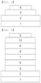
- the organic light emitting device may have structures as illustrated in FIGs. 1 and 2 .
- the organic light emitting device may be formed with a substrate (1), an anode (2), an organic material layer (3) and a cathode (4).
- the compound represented by Chemical Formula 1 is included in the organic material layer (3).
- the organic light emitting device may be formed with a substrate (1), an anode (2), a hole injection layer (5), a hole transfer layer (6), a hole control layer (7), a light emitting layer (8), an electron transfer layer (9), an electron injection layer (10) and a cathode (4).
- the compound represented by Chemical Formula 1 is included in the light emitting layer (8).
- the compound represented by Chemical Formula 1 is included in any one of the hole transfer layer (5), the hole transfer layer (6) and the hole control layer (7).
- the compound represented by Chemical Formula 1 is included in the electron transfer layer (9) or the electron injection layer (10).
- the structure of the organic light emitting device is not limited to FIG. 1 and FIG. 2 , and may be any one of the following structures.
- the organic material layers may be formed with materials the same as or different from each other.
- the organic light emitting device of the present specification may be manufactured by consecutively laminating a first electrode, an organic material layer and a second electrode on a substrate.
- the organic light emitting device may be manufactured by forming an anode on a substrate by depositing a metal, a metal oxide having conductivity, or an alloy thereof using a physical vapor deposition (PVD) method such as sputtering or e-beam evaporation, and forming an organic material layer including a hole injection layer, a hole transfer layer, a light emitting layer and an electron transfer layer thereon, and then depositing a material capable of being used as a cathode thereon.
- PVD physical vapor deposition
- the compound represented by Chemical Formula 1 may be formed into an organic material layer using a solution coating method as well as a vacuum deposition method when manufacturing the organic light emitting device.
- the solution coating method means spin coating, dip coating, doctor blading, inkjet printing, screen printing, a spray method, roll coating and the like, but is not limited thereto.
- the organic light emitting device may also be manufactured by consecutively depositing a cathode material, an organic material layer and an anode material on a substrate (International Patent Application Laid-Open Publication No. 2003/012890).
- the manufacturing method is not limited thereto.
- anode material materials having large work function are normally preferred so that hole injection to an organic material layer is smooth.
- the anode material capable of being used in the present disclosure include metals such as vanadium, chromium, copper, zinc and gold, or alloys thereof; metal oxides such as zinc oxide, indium oxide, indium tin oxide (ITO) and indium zinc oxide (IZO); combinations of metals and oxides such as ZnO:Al or SnO 2 :Sb; conductive polymers such as poly(3-methylthiophene), poly[3,4-(ethylene-1,2-dioxy)thiophene] (PEDOT), polypyrrole and polyaniline, but are not limited thereto.
- the cathode material materials having small work function are normally preferred so that electron injection to an organic material layer is smooth.
- the cathode material include metals such as magnesium, calcium, sodium, potassium, titanium, indium, yttrium, lithium, gadolinium, aluminum, silver, tin and lead, or alloys thereof; multilayer structure materials such as LiF/Al or LiO 2 /Al, and the like, but are not limited thereto.
- the hole injection layer is a layer injecting holes received from an electrode to a light emitting layer or an adjacent layer provided on a light emitting layer side.
- the hole injection material compounds having an ability to transfer holes, therefore, having a hole injection effect in an anode, having an excellent hole injection effect for a light emitting layer or a light emitting material, preventing excitons generated in the light emitting layer from moving to an electron injection layer or an electron injection material, and in addition thereto, having an excellent thin film forming ability are preferably used.
- the highest occupied molecular orbital (HOMO) of the hole injection material is preferably in between the work function of an anode material and the HOMO of surrounding organic material layers.
- the hole injection material examples include metal porphyrins, oligothiophene, arylamine-based organic materials, hexanitrile hexaazatriphenylene-based organic materials, quinacridone-based organic materials, perylene-based organic materials, anthraquinone, and polyaniline- and polythiophene-based conductive polymers, and the like, but are not limited thereto.
- the hole transfer layer is a layer receiving holes from a hole injection layer and transferring the holes to a light emitting layer or an adjacent layer provided on a light emitting layer side.
- the hole transfer material materials capable of receiving holes from an anode or a hole injection layer, moving the holes to a light emitting layer, and having high mobility for the holes are suited.
- the hole transfer material include arylamine-based organic materials, conductive polymers, block copolymers having conjugated parts and non-conjugated parts together, and the like, but are not limited thereto.
- the hole control layer is a layer controlling performance of a whole device by preventing electrons inflowing from a light emitting layer to an anode and by controlling a flow of holes inflowing to the light emitting layer.
- the hole control material compounds having abilities of preventing electrons inflowing from a light emitting layer to an anode, and controlling a flow of holes injected to the light emitting layer or the light emitting material are preferred.
- arylamine-based organic materials may be used as the hole control layer, however, the hole control layer is not limited thereto.
- the light emitting material is a material capable of emitting light in a visible light region by receiving holes and electrons from a hole transfer layer and an electron transfer layer, respectively, and binding the holes and the electrons, and is preferably a material having favorable quantum efficiency for fluorescence or phosphorescence.
- Alq 3 8-hydroxy-quinoline aluminum complexes
- carbazole-based compounds dimerized styryl compounds
- BAlq 10-hydroxybenzoquinoline-metal compounds
- benzoxazole-, benzothiazole- and benzimidazole-based compounds poly(p-phenylenevinylene) (PPV)-based polymers
- spiro compounds polyfluorene; rubrene, and the like, but are not limited thereto.
- the light emitting layer may include a host material and a dopant material.
- the host material may include fused aromatic ring derivatives, heteroring-containing compounds or the like. Specifically, as the fused aromatic ring derivative, anthracene derivatives, pyrene derivatives, naphthalene derivatives, pentacene derivatives, phenanthrene compounds, fluoranthene compounds and the like may be included, and as the heteroring-containing compound, carbazole derivatives, dibenzofuran derivatives, ladder-type furan compounds, pyrimidine derivatives and the like may be included, however, the host material is not limited thereto.
- the dopant material of the light emitting layer may include aromatic amine derivatives, styrylamine compounds, boron complexes, fluoranthene compounds, metal complexes and the like.
- the aromatic amine derivative is a fused aromatic ring derivative having a substituted or unsubstituted arylamine group, and arylamine group-including pyrene, anthracene, chrysene, peryflanthene and the like may be used.
- styrylamine compound compounds in which substituted or unsubstituted arylamine is substituted with at least one arylvinyl group may be used.
- styralamine compound may include styrylamine, styryldiamine, styryltriamine, styryltetramine and the like, but are not limited thereto.
- metal complex iridium complexes, platinum complexes and the like may be used, however, the metal complex is not limited thereto.
- the electron control layer is a layer controlling performance of a whole device by blocking holes inflowing from a light emitting layer to a cathode and by controlling electrons inflowing to the light emitting layer.
- the electron control material compounds having abilities of preventing holes inflowing from a light emitting layer to a cathode, and controlling electrons injected to the light emitting layer or the light emitting material are preferred.
- the electron control material proper materials may be used depending on the constitution of the organic material layers used in a device.
- the electron control layer is placed between a light emitting layer and a cathode, and is preferably provided directly in contact with a light emitting layer.
- the electron transfer layer is a layer receiving electrons from an electron injection layer and transferring the electrons to a light emitting layer.
- the electron transfer material materials capable of favorably receiving electrons from a cathode, moving the electrons to a light emitting layer, and having high mobility for the electrons are suited.
- the electron transfer material may include Al complexes of 8-hydroxyquinoline; complexes including Alq 3 ; organic radical compounds; hydroxyflavon-metal complexes, and the like, but are not limited thereto.
- the electron transfer layer may be used together with any desired cathode material as used in the art. In one embodiment, as the cathode material, materials having low work function; and an aluminum layer or a silver layer may be used.
- Examples of the material having low work function may include cesium, barium, calcium, ytterbium, samarium and the like, and after forming a layer with the above-mentioned material, an aluminum layer or a silver layer may be formed on the layer.
- the electron injection layer is a layer injecting electrons received from an electrode to a light emitting layer.
- the electron injection material compounds having an electron transferring ability, having an electron injection effect from a cathode, having an excellent electron injection effect for a light emitting layer or light emitting material, and preventing excitons generated in the light emitting layer from moving to a hole injection layer, and in addition thereto, having an excellent thin film forming ability are preferably used.
- fluorenone anthraquinodimethane, diphenoquinone, thiopyran dioxide, oxazole, oxadiazole, triazole, imidazole, perylene tetracarboxylic acid, fluorenylidene methane, anthrone or the like, and derivatives thereof, metal complex compounds, nitrogen-containing 5-membered ring derivatives, and the like, but are not limited thereto.
- the metal complex compound includes 8-hydroxyquinolinato lithium, bis(8-hydroxyquinolinato)zinc, bis(8-hydroxyquinolinato)copper, bis(8-hydroxyquinolinato)manganese, tris(8-hydroxyquinolinato)aluminum, tris(2-methyl-8-hydroxyquinolinato) aluminum, tris(8-hydroxyquinolinato)gallium, bis(10-hydroxybenzo[h]quinolinato)beryllium, bis(10-hydroxybenzo[h]quinolinato)zinc, bis(2-methyl-8-quinolinato)chlorogallium, bis(2-methyl-8-quinolinato)(o-cresolato)gallium, bis(2-methyl-8-quinolinato)(1-naphtholato)aluminum, bis(2-methyl-8-quinolinato)(2-naphtholato)gallium and the like, but is not limited thereto.
- the organic light emitting device may be a top-emission type, a bottom-emission type or a dual-emission type depending on the materials used.
- Fluoro-2-iodobenzene (66 g, 299.99 mmol) and (3-bromo-6-chloro-2-hydroxyphenyl)boronic acid (75.38 g, 299.99 mmol) were dissolved in tetrahydrofuran (THF) (800 ml).
- THF tetrahydrofuran
- a 2 M sodium carbonate (Na 2 CO 3 ) solution (500 mL) and tetrakis(triphenylphosphine)palladium (0) [Pd(PPh 3 ) 4 ] (10.4 g, 9 mmol) were introduced thereto, and the result was refluxed for 12 hours.
- 1,3-Dibromo-4-chloro-2-nitrobenzene (87.03 g, 275.98 mmol) and (2-nitrophenyl)boronic acid (46.1 g, 275.98 mmol) were dissolved in tetrahydrofuran (THF) (800 ml).
- THF tetrahydrofuran
- a 2 M sodium carbonate (Na 2 CO 3 ) solution (500 mL)
- tetrakis(triphenylphosphine)palladium(0) [Pd(PPh 3 ) 4 ] (9.6 g, 8.28 mmol) were introduced thereto, and the result was refluxed for 6 hours at 50°C.
- a glass substrate on which indium tin oxide (ITO) was coated as a thin film to a thickness of 130 nm was placed in detergent-dissolved distilled water and ultrasonic cleaned.
- ITO indium tin oxide
- a product of Fischer Co. was used as the detergent, and as the distilled water, distilled water filtered twice with a filter manufactured by Millipore Co. was used.
- the substrate was ultrasonic cleaned with solvents of isopropyl alcohol, acetone and methanol, then dried, and then transferred to a plasma cleaner.
- the substrate was cleaned for 5 minutes using oxygen plasma, and then transferred to a vacuum depositor.
- a hole injection layer was formed by thermal vacuum depositing the following Compound HI-1 to a thickness of 5 nm.
- a hole transfer layer was formed on the hole injection layer by thermal vacuum depositing the following Compound HT-1 to a thickness of 25 nm, and on the HT-1 deposited film, a hole control layer was formed by vacuum depositing the following Compound HT-2 to a thickness of 5 nm.
- a light emitting layer having a thickness of 40 nm was formed on the HT-2 deposited film by co-depositing Compound 1 prepared above and the following Compound Dp-25 in a weight ratio of 88:12.
- an electron transfer layer was formed by vacuum depositing the following Compound ET-1 to a thickness of 25 nm, and an electron injection layer was formed thereon by vacuum depositing (thickness 10 nm) the following Compound ET-2 and LiQ in a weight ratio of 98:2.
- a cathode was formed by depositing aluminum to a thickness of 100 nm.
- Examples 19 to 24 and Comparative Examples 5 and 6 organic light emitting devices were manufactured in the same manner as in Example 1 except that compounds described in the following Table 1 were used in a weight ratio of 1:1 instead of Compound 1. Taking Example 19 as an example, Compound 1 and Compound H-2 were used in a weight ratio of 1:1 instead of Compound 1 in Example 1.
- T 95 means time taken for luminance decreasing to 95% when employing initial luminance at current density of 20 mA/cm 2 as 100%.
- Examples 1 to 18 and Comparative Examples 1 and 2 are examples of a device using a single host in a light emitting layer.
- Compound C1 used in Comparative Example 1 is a compound in which triazine is substituted with two dibenzothiophenyl groups. From Table 1, it was identified that the devices of Examples 1 to 18 had lifetime properties enhanced by approximately 55% to 88% compared to the device of Comparative Example 1.
- Compound C2 used in Comparative Example 2 is a compound in which triazine is substituted with one dibenzofuranyl group and two aryl groups. From Table 1, it was identified that the devices of Examples 1 to 18 had lifetime properties enhanced by approximately 37% to 75% compared to the device of Comparative Example 2.
- Compound C3 used in Comparative Example 3 is a compound in which a phenyl group, one of substituents of the triazine, is substituted with a heteroaryl group. From Table 1, it was identified that the devices of Examples 1 to 18 had current efficiency enhanced by approximately 4.3% to 15.5% compared to the device of Comparative Example 3.
- Compound C4 used in Comparative Example 4 is a compound in which one dibenzofuranyl group of the two dibenzofuranyl groups, a substituent of the triazine, is unsubstituted. From Table 1, it was identified that the devices of Examples 1 to 18 had current efficiency enhanced by approximately 4.7% to 17% compared to the device of Comparative Example 4.
- Examples 19 to 24 are examples of a device using two types of hosts in a light emitting layer. When comparing Examples 19 to 24 and Examples 1 to 18, it was identified that, when using two types of hosts in a light emitting layer, current efficiency increased more, and particularly, lifetime properties were significantly enhanced.
- the devices of Examples 19 to 24 using the compound of the present disclosure also had excellent current efficiency and lifetime properties compared to the devices of Comparative Examples 5 and 6.
- a dibenzofuranyl group and/or a dibenzosilole group directly bond to triazine having strong electron properties, and the dibenzofuranyl group and/or the dibenzosilole group are substituted with an aryl group and a heteroaryl group having strong hole properties.
- the compound represented by Chemical Formula 1 of the present disclosure may be understood to have advantages in terms of device efficiency and lifetime since holes and electros are smoothly inflowing, and holes and electrons are well balanced.
Description
- The present disclosure relates to a compound represented by Chemical Formula 1, and an organic light emitting device including the same.
- An organic light emission phenomenon generally refers to a phenomenon converting electrical energy to light energy using an organic material. An organic light emitting device using an organic light emission phenomenon normally has a structure including an anode, a cathode, and an organic material layer therebetween. Herein, the organic material layer is formed in a multilayer structure formed with different materials in order to increase efficiency and stability of the organic light emitting device, and for example, may be formed with a hole injection layer, a hole transfer layer, a light emitting layer, an electron transfer layer, an electron injection layer and the like. When a voltage is applied between the two electrodes in such an organic light emitting device structure, holes and electrons are injected to the organic material layer from the anode and the cathode, respectively, and when the injected holes and electrons meet, excitons are formed, and light emits when these excitons fall back to the ground state. The
compound 2,4-bis(2-dibenzofuranyl)-6-phenyl-1,3,5-triazine used in OLEDs is disclosed by YU Jun Kang et al. in Journal of Industrial and Engineering Chemistry 62 (2018) 258-264. - Development of new materials for such an organic light emitting device has been continuously required.
- Prior Art Documents
Korean Patent Application Laid-Open Publication No. 10-2008-0109671 - The present specification is directed to providing a compound represented by Chemical Formula 1.
- The present specification is directed to providing an organic light emitting device having, by including the compound represented by Chemical Formula 1, a low driving voltage, high efficiency, or excellent lifetime properties.
- One embodiment of the present specification provides a compound represented by the following Chemical Formula 1.


- X1 is O or SiRaRb,
- X2 is O or SiRcRd,
- Ra to Rd are the same as or different from each other, and each independently hydrogen; deuterium; an alkyl group; or an aryl group,
- any one of A1 to A4 and A'1 to A'4 is a linking group bonding to triazine, any one is Ar1, and the rest are hydrogen,
- any one of B1 to B4 and B'1 to B'4 is a linking group bonding to triazine, any one is Ar2, and the rest are hydrogen,
- Ar1 and Ar2 are the same as or different from each other, and each independently an aryl group; or a heteroaryl group unsubstituted or substituted with an aryl group.
- Another embodiment of the present specification provides an organic light emitting device comprising a first electrode, a second electrode, and one or more organic material layers provided between the first electrode and the second electrode, wherein the organic material layer comprises the compound represented by Chemical Formula 1 described above.
- A compound represented by Chemical Formula 1 can be included in a hole injection layer; a hole transfer layer; a layer carrying out hole transfer and injection at the same time; a hole control layer; an electron control layer; an electron injection layer; an electron transfer layer and a layer carrying out electron transfer and injection at the same time; and particularly in a light emitting layer of an organic light emitting device.
- In some embodiments, an organic light emitting device including the compound of Chemical Formula 1 can have enhanced efficiency, lowered driving voltage, or enhanced lifetime properties.
-
-
FIG. 1 illustrates an example of an organic light emitting device formed with a substrate (1), an anode (2), an organic material layer (3) and a cathode (4). -
FIG. 2 illustrates an example of an organic light emitting device formed with a substrate (1), an anode (2), a hole injection layer (5), a hole transfer layer (6), a hole control layer (7), a light emitting layer (8), an electron transfer layer (9), an electron injection layer (10) and a cathode (4). -
- 1: Substrate
- 2: Anode
- 3: Organic Material Layer
- 4: Cathode
- 5: Hole Injection Layer
- 6: Hole Transfer Layer
- 7: Hole Control Layer
- 8: Light Emitting Layer
- 9: Electron Transfer Layer
- 10: Electron Injection Layer
- Hereinafter, the present disclosure will be described in more detail.
- One embodiment of the present disclosure provides a compound represented by Chemical Formula 1.
- In the present specification,

- In the present specification, a term such as `include' or 'have' means the presence of features or constituents described in the specification, and is not to exclude in advance the possibility of adding one or more other features or constituents.
- In the present specification, a description of a part such as a region or a layer being provided above or on another part includes not only a case of the part being directly above the another part but a case of still another region, layer or the like being provided therebetween.
- Examples of the substituents are described below, however, the substituents are not limited thereto.
- In the present specification, an aryl group means a totally or partially unsaturated substituted or unsubstituted monocyclic ring or polycyclic ring. According to one embodiment, the aryl group has 6 to 25 carbon atoms. According to one embodiment, the aryl group has 6 to 20 carbon atoms. According to one embodiment, the aryl group has 6 to 18 carbon atoms. According to one embodiment, the aryl group has 6 to 13 carbon atoms. According to one embodiment, the aryl group has 6 to 12 carbon atoms. According to one embodiment, the aryl group has 6 carbon atoms.
- The aryl group may be a monocyclic aryl group or a polycyclic aryl group. Examples of the monocyclic aryl group may include a phenyl group, a biphenyl group, a terphenyl group and the like, but are not limited thereto. Examples of the polycyclic aryl group may include a naphthyl group, an anthracenyl group, a phenanthrenyl group, a perylenyl group, a fluoranthenyl group, a triphenylenyl group, a pyrenyl group, a tetracenyl group, a chrysenyl group, a fluorenyl group, an indenyl group, an acenaphthyl group, a benzofluorenyl group and the like, but are not limited thereto.
- In the present specification, the fluorenyl group may be substituted, and two substituents may bond to each other to form a spiro structure.
- Examples of the substituted fluorenyl group may include


- In the present specification, the heteroaryl group is a cyclic group including one or more of N, O and S as a heteroatom, and although not limited thereto, the number of carbon atoms is preferably from 2 to 40. According to one embodiment, the number of carbon atoms of the heteroaryl group is from 2 to 30. According to another embodiment, the number of carbon atoms of the heteroaryl group is from 2 to 20. Examples of the heteroaryl group may include a thiophenyl group, a furanyl group, a pyrrolyl group, an imidazolyl group, a thiazolyl group, an oxazolyl group, an oxadiazolyl group, a triazolyl group, a pyridinyl group, a bipyridinyl group, a pyrimidinyl group, a diazinyl group, a triazinyl group, a triazolyl group, an acridinyl group, a carbolinyl group, an acenaphthoquinoxalinyl group, an indenoquinazolinyl group, an indenoisoquinolinyl group, an indenoquinolinyl group, a pyridoindolyl group, a pyridazinyl group, a pyrazinyl group, a quinolinyl group, a quinazolinyl group, a quinoxalinyl group, a phthalazinyl group, a pyridopyrimidinyl group, a pyridopyrazinyl group, a pyrazinopyrazinyl group, an isoquinolinyl group, an indolyl group, a carbazolyl group, a benzoxazolyl group, a benzimidazolyl group, a benzothiazolyl group, a benzocarbazolyl group, a benzothiophenyl group, a dibenzothiophenyl group, a benzofuranyl group, a dibenzofuranyl group, a phenanthrolinyl group, a thiazolyl group, an isoxazolyl group, an oxadiazolyl group, a thiadiazolyl group, a phenoxazinyl group, a phenothiazinyl group and the like, but are not limited thereto.
- In one embodiment of the present specification, X1 is O, and X2 is O or SiRcRd.
- In one embodiment of the present specification, X1 is SiRaRb, and X2 is O or SiRcRd.
- In one embodiment of the present specification, X1 is O, and X2 is O.
- In one embodiment of the present specification, X1 is SiRaRb, and X2 is O.
- In one embodiment of the present specification, X1 is O, and X2 is SiRcRd.
- In one embodiment of the present specification, X1 is SiRaRb, and X2 is SiRcRd.
- In one embodiment of the present specification, Ra to Rd are the same as or different from each other, and each independently hydrogen; deuterium; an alkyl group having 1 to 10 carbon atoms; or an aryl group having 6 to 20 carbon atoms.
- In one embodiment of the present specification, Ra to Rd are the same as or different from each other, and each independently hydrogen; deuterium; an alkyl group having 1 to 6 carbon atoms; or an aryl group having 6 to 13 carbon atoms.
- In one embodiment of the present specification, Ra to Rd are the same as or different from each other, and each independently hydrogen; deuterium; an alkyl group having 1 to 4 carbon atoms; or an aryl group having 6 to 10 carbon atoms.
- In one embodiment of the present specification, Ra to Rd are the same as or different from each other, and each independently hydrogen; deuterium; a methyl group; or a phenyl group.
- In one embodiment of the present specification, any one of A1 to A4 is a linking group bonding to triazine, any one is Ar1, the rest are hydrogen, and A'1 to A'4 are hydrogen.
- In one embodiment of the present specification, any one of A1 to A4 is a linking group bonding to triazine, the rest are hydrogen, any one of A'1 to A'4 is Ar1, and the rest are hydrogen.
- In one embodiment of the present specification, any one of B1 to B4 is a linking group bonding to triazine, any one is Ar2, the rest are hydrogen, and B'1 to B'4 are hydrogen.
- In one embodiment of the present specification, any one of B1 to B4 is a linking group bonding to triazine, the rest are hydrogen, any one of B'1 to B'4 is Ar2, and the rest are hydrogen.
- In one embodiment of the present specification, an aromatic 6-membered ring included in the compound represented by
Chemical Formula 1 is 10 or less. WhenChemical Formula 1 includes 11 or more aromatic 6-membered rings, a sublimation temperature of the compound increases due to an increase in the molecular weight, which may cause a problem in device thermal stability. In the compound represented byChemical Formula 1, it may be interpreted that triazine includes one aromatic 6-membered ring, and benzofuran includes two aromatic 6-membered rings (benzene rings). - In one embodiment of the present specification, Ar1 and Ar2 are the same as or different from each other, and each independently an aryl group; or a heteroaryl group unsubstituted or substituted with an aryl group and comprising one or more of N, O and S.
- In one embodiment of the present specification, Ar1 and Ar2 are the same as or different from each other, and each independently an aryl group; or a heteroaryl group unsubstituted or substituted with an aryl group and comprising a pentagonal ring.
- In one embodiment of the present specification, Ar1 and Ar2 are the same as or different from each other, and each independently an aryl group having 6 to 25 carbon atoms; or a heteroaryl group having 2 to 25 carbon atoms unsubstituted or substituted with an aryl group.
- In one embodiment of the present specification, Ar1 and Ar2 are the same as or different from each other, and each independently an aryl group; or a heteroaryl group unsubstituted or substituted with an aryl group having 6 to 18 carbon atoms.
- In one embodiment of the present specification, Ar1 and Ar2 are the same as or different from each other, and each independently an aryl group; or a heteroaryl group unsubstituted or substituted with an aryl group having 6 to 12 carbon atoms.
- In one embodiment of the present specification, Ar1 and Ar2 are the same as or different from each other, and each independently an aryl group; or a heteroaryl group unsubstituted or substituted with an aryl group and comprising pyrrole, furan, thiophene, imidazole, oxazole or thiazole.
- In one embodiment of the present specification, Ar1 and Ar2 are the same as or different from each other, and each independently an aryl group having 6 to 20 carbon atoms; or a heteroaryl group having 2 to 20 carbon atoms unsubstituted or substituted with an aryl group.
- In one embodiment of the present specification, Ar1 and Ar2 are the same as or different from each other, and each independently an aryl group having 6 to 20 carbon atoms; or a heteroaryl group having 7 to 20 carbon atoms unsubstituted or substituted with an aryl group.
- In one embodiment of the present specification, Ar1 and Ar2 are the same as or different from each other, and each independently an aryl group having 6 to 18 carbon atoms; or a heteroaryl group having 2 to 24 carbon atoms unsubstituted or substituted with an aryl group.
- In one embodiment of the present specification, Ar1 and Ar2 are the same as or different from each other, and each independently an aryl group having 6 to 18 carbon atoms; or a heteroaryl group having 2 to 20 carbon atoms unsubstituted or substituted with an aryl group.
- In one embodiment of the present specification, Ar1 and Ar2 are the same as or different from each other, and each independently an aryl group having 6 to 18 carbon atoms; or a heteroaryl group having 2 to 16 carbon atoms unsubstituted or substituted with an aryl group.
- In one embodiment of the present specification, Ar1 and Ar2 are the same as or different from each other, and each independently an aryl group having 6 to 18 carbon atoms; or a heteroaryl group having 2 to 20 carbon atoms unsubstituted or substituted with an aryl group.
- In one embodiment of the present specification, Ar1 and Ar2 are the same as or different from each other, and each independently an aryl group having 6 to 15 carbon atoms; or a heteroaryl group having 2 to 20 carbon atoms unsubstituted or substituted with an aryl group.
- In one embodiment of the present specification, Ar1 and Ar2 are the same as or different from each other, and each independently an aryl group having 6 to 13 carbon atoms; or a heteroaryl group having 2 to 16 carbon atoms unsubstituted or substituted with an aryl group.
- In one embodiment of the present specification, Ar1 and Ar2 are the same as or different from each other, and each independently an aryl group having 6 to 12 carbon atoms; or a heteroaryl group having 2 to 12 carbon atoms unsubstituted or substituted with an aryl group.
- In one embodiment of the present specification, Ar1 and Ar2 are the same as or different from each other, and each independently a phenyl group; a biphenyl group; a terphenyl group; a dibenzothiophenyl group; a dibenzofuranyl group; a carbazolyl group unsubstituted or substituted with a phenyl group; a benzothiazolyl group; a benzimidazolyl group unsubstituted or substituted with a phenyl group; or a benzoxazolyl group.
- In one embodiment of the present specification,
Chemical Formula 1 is represented by any one of the followingChemical Formula 2 toChemical Formula 4. - In the following
Chemical Formula 2 toChemical Formula 4, X1, X2, Ar1 and Ar2 have the same definitions as inChemical Formula 1,
Chemical Formula 2, - any one of A1 to A4 is a linking group bonding to triazine, and the rest are hydrogen,
- any one of A'1 to A'4 is Ar1, and the rest are hydrogen,
- any one of B1 to B4 is a linking group bonding to triazine, and the rest are hydrogen, and
- any one of B'1 to B'4 is Ar2, and the rest are hydrogen,


Chemical Formula 3,- any one of A1 to A4 is a linking group bonding to triazine, any one is Ar1, and the rest are hydrogen,
- any one of B1 to B4 is a linking group bonding to triazine, and the rest are hydrogen, and
- any one of B'1 to B'4 is Ar2, and the rest are hydrogen,

Chemical Formula 4,- any one of A1 to A4 is a linking group bonding to triazine, any one is Ar1, and the rest are hydrogen, and
- any one of B1 to B4 is a linking group bonding to triazine, any one is Ar2, and the rest are hydrogen.
- In one embodiment of
Chemical Formula 2, when a linking unit bonding to triazine among A1 to A4 is Ax (x is an integer of 1 to 4), a linking unit bonding to triazine among B1 to B4 is By (y is an integer of 1 to 4), a linking unit bonding to Ar1 among A'1 to A'4 is A'x' (x' is an integer of 1 to 4), and a linking unit bonding to Ar2 among B'1 to B'4 is B'y' (y' is an integer of 1 to 4), x is the same as y, and x' is the same as y' . - In one embodiment of
Chemical Formula 3, when a linking unit bonding to triazine among A1 to A4 is Am (m is an integer of 1 to 4), a linking unit bonding to triazine among B1 to B4 is Bn (n is an integer of 1 to 4), a linking unit bonding to Ar1 among A1 to A4 is Am' (m' is an integer of 1 to 4), and a linking unit bonding to Ar2 among B'1 to B'4 is B'n' (n' is an integer of 1 to 4), m is the same as n, and m' is the same as n' . - In one embodiment of
Chemical Formula 4, when a linking unit bonding to triazine among A1 to A4 is Ap (p is an integer of 1 to 4), a linking unit bonding to triazine among B1 to B4 is Bq (q is an integer of 1 to 4), a linking unit bonding to Ar1 among A1 to A4 is Ap' (p' is an integer of 1 to 4), and a linking unit bonding to Ar2 among B1 to B4 is Bq' (q' is an integer of 1 to 4), p is the same as q, and p' is the same as q'. - In one embodiment of the present specification,
Chemical Formula 1 is represented by any one of the following Chemical Formula 1-A to Chemical Formula 1-C.


Ra to Rd, A1 to A4, A'1 to A'4, B1 to B4 and B'1 to B'4 have the same definitions as inChemical Formula 1. - In one embodiment of the present specification, the compound represented by
Chemical Formula 1 is any one selected from among the following compounds.


- According to one embodiment of the present specification, the compound represented by
Chemical Formula 1 described above may be prepared according to the followingGeneral Formula 1 orGeneral Formula 2.


- In
General Formula 1 andGeneral Formula 2, Ra to Rd, Ar1 and Ar2 have the same definitions as inChemical Formula 1. -
General Formulae Chemical Formula 1, and a method for synthesizing the compound represented byChemical Formula 1 is not limited toGeneral Formulae - One embodiment of the present specification provides an organic light emitting device comprising the compound represented by
Chemical Formula 1. - One embodiment of the present specification provides an organic light emitting device comprising a first electrode, a second electrode, and one or more organic material layers provided between the first electrode and the second electrode, wherein the organic material layer comprises the compound represented by
Chemical Formula 1 described above. - The organic material layer of the organic light emitting device of the present specification may be formed in a single layer structure, but may also be formed in a multilayer structure in which two or more organic material layers are laminated. For example, the organic light emitting device of the present disclosure may have a structure comprising a hole injection layer, a hole transfer layer, a layer carrying out hole transfer and injection at the same time, a hole control layer, a light emitting layer, an electron control layer, an electron transfer layer, an electron injection layer, a layer carrying out electron transfer and injection at the same time and the like as the organic material layer.
- In one embodiment of the present specification, the organic material layer comprising the compound represented by
Chemical Formula 1 has a thickness of 5 nm or greater; 10 nm or greater; 20 nm or greater; or 30 nm or greater, and 80 nm or less; 70 nm or less; 60 nm or less; or 50 nm or less. - In one embodiment of the present specification, the organic material layer comprises a light emitting layer, and the light emitting layer comprises the compound represented by
Chemical Formula 1. - In one embodiment of the present specification, the light emitting layer comprising the compound represented by
Chemical Formula 1 has a thickness of 25 nm to 55 nm; or 30 nm to 50 nm. - In one embodiment of the present specification, the organic material layer comprising the compound represented by
Chemical Formula 1 further includes a host. - In one embodiment of the present specification, the light emitting layer comprising the compound represented by
Chemical Formula 1 further comprises a host. When the light emitting layer including the compound represented byChemical Formula 1 further comprises a host, device lifetime properties may be greatly enhanced. - In one embodiment of the present specification, the host is a carbazole derivative; or a biscarbazole derivative.
- In one embodiment of the present specification, the host is a substituted or unsubstituted biscarbazole.
- In one embodiment of the present specification, the host is a compound represented by the following Chemical Formula H.


- Ar11 to Ar14 are the same as or different from each other, and each independently hydrogen; deuterium; a substituted or unsubstituted alkyl group; a substituted or unsubstituted aryl group; or a substituted or unsubstituted heteroaryl group,
- L11 and L12 are the same as or different from each other, and each independently a direct bond; a substituted or unsubstituted divalent aryl group; or a substituted or unsubstituted divalent heteroaryl group,
- k1 and k2 are each independently an integer of 0 to 7,
- when k1 is 2 or greater, Ar12s are the same as or different from each other, and
- when k2 is 2 or greater, Ar14s are the same as or different from each other.
- In one embodiment of the present specification, Ar11 and Ar12 are the same as or different from each other, and each independently a substituted or unsubstituted aryl group; or a substituted or unsubstituted heteroaryl group.
- In one embodiment of the present specification, Ar11 and Ar12 are the same as or different from each other, and each independently a substituted or unsubstituted aryl group having 6 to 30 carbon atoms; or a substituted or unsubstituted heteroaryl group having 2 to 30 carbon atoms.
- In one embodiment of the present specification, Ar11 and Ar12 are the same as or different from each other, and each independently a substituted or unsubstituted aryl group having 6 to 18 carbon atoms; or a substituted or unsubstituted heteroaryl group having 2 to 15 carbon atoms.
- In one embodiment of the present specification, Ar11 and Ar12 are the same as or different from each other, and each independently an aryl group unsubstituted or substituted with an aryl group or a heteroaryl group; or a heteroaryl group unsubstituted or substituted with an aryl group or a heteroaryl group.
- In one embodiment of the present specification, Ar11 and Ar12 are the same as or different from each other, and each independently a phenyl group; a biphenyl group; or a triazinyl group unsubstituted or substituted with a phenyl group or a biphenyl group.
- In one embodiment of the present specification, Ar13 and Ar14 are the same as or different from each other, and each independently hydrogen; deuterium; an alkyl group; an aryl group unsubstituted or substituted with an aryl group or a heteroaryl group; or a heteroaryl group unsubstituted or substituted with an aryl group or a heteroaryl group.
- In one embodiment of the present specification, Ar13 and Ar14 are the same as or different from each other, and each independently hydrogen; a methyl group; a phenyl group; a biphenyl group; or a carbazolyl group unsubstituted or substituted with a phenyl group.
- In one embodiment of the present specification, Ar13 and Ar14 are the same as or different from each other, and each independently hydrogen; or deuterium.
- In one embodiment of the present specification, L11 and L12 are the same as or different from each other, and each independently a direct bond; a substituted or unsubstituted divalent aryl group having 6 to 20 carbon atoms; or a substituted or unsubstituted divalent heteroaryl group having 2 to 20 carbon atoms.
- In one embodiment of the present specification, L11 and L12 are the same as or different from each other, and each independently a direct bond; a divalent aryl group unsubstituted or substituted with an aryl group; or a divalent heteroaryl group unsubstituted or substituted with an aryl group.
- In one embodiment of the present specification, L11 and L12 are the same as or different from each other, and each independently a direct bond; or a phenylene group.
- In one embodiment of the present specification, the light emitting layer comprising the compound represented by
Chemical Formula 1 further comprises a dopant. - In one embodiment of the present specification, the light emitting layer comprising the compound represented by
Chemical Formula 1 further comprises a dopant, and a content of the dopant is greater than or equal to 0.1 parts by weight and less than or equal to 20 parts by weight; or greater than or equal to 1 parts by weight and less than or equal to 15 parts by weight with respect to a total 100 parts by weight of the light emitting layer. - In one embodiment of the present specification, the dopant is an iridium complex.
- In one embodiment of the present specification, the dopant is a compound represented by the following Chemical Formula Dp.

- G1 to G4 are the same as or different from each other, and each independently hydrogen; deuterium; a halogen group; an alkyl group; an aryl group; -OR11; -C(=O)R12; an aryl group; or a heteroaryl group, and adjacent G1s; adjacent G2s; adjacent G3s; or adjacent G4s can bond to each other to form a ring unsubstituted or substituted with deuterium; a halogen group; an alkyl group; an aryl group; -OR13; -C(=O)R14; an aryl group; or a heteroaryl group,
- R11 to R14 are the same as or different from each other, and each independently an alkyl group; or an aryl group,
- Cy is an aromatic ring,
- g1 is an integer of 0 or greater, and when g1 is 2 or greater, G1s are the same as or different from each other,
- g2 is an integer of 0 to 4, and when g2 is 2 or greater, G2s are the same as or different from each other,
- g3 is an integer of 0 to 4, and when g3 is 2 or greater, G3s are the same as or different from each other,
- g4 is an integer of 0 to 4, and when g4 is 2 or greater, G4s are the same as or different from each other,
- p1 is 1 or 2, p2 is 1 or 2, a sum of p1 and p2 is 3,
- when p1 is 2,

- when p2 is 2,

- In one embodiment of the present specification, Cy is an aromatic hydrocarbon ring; or an aromatic heteroring.
- In one embodiment of the present specification, Cy is an aromatic hydrocarbon ring; or an aromatic heteroring comprising at least one element selected form the group consisting of N, S and O.
- In one embodiment of the present specification, Cy is an aromatic ring having 3 to 14 carbon atoms.
- In one embodiment of the present specification, Cy is an aromatic ring having 3 to 10 carbon atoms.
- In one embodiment of the present specification, Cy is benzene; thiophene; or benzothiophene.
- In one embodiment of the present specification, Chemical Formula Dp is represented by the following Chemical Formula Dp' .

- G1 to G4, g2, g3, g4, p1 and p2 have the same definitions as in Chemical Formula Dp, and
- g1 is an integer of 0 to 4, and when g1 is 2 or greater, G1s are the same as or different from each other.
- In one embodiment of the present specification, G1 to G4 are the same as or different from each other, and each independently hydrogen; deuterium; a halogen group; an alkyl group; an aryl group; -OR11; -C(=O)R12; an aryl group; or a heteroaryl group, and adjacent G1s; adjacent G2s; adjacent G3s; or adjacent G4s can bond to each other to form a benzene ring unsubstituted or substituted with deuterium; a halogen group; an alkyl group; an aryl group; -OR13; -C(=O)R14; an aryl group; or a heteroaryl group.
- In one embodiment of the present specification, the organic material layer comprises a hole injection layer; a hole transfer layer; a layer carrying out hole transfer and injection at the same time; a hole control layer; an electron control layer; an electron injection layer; an electron transfer layer; or a layer carrying out electron transfer and injection at the same time, and the hole injection layer; the hole transfer layer; the layer carrying out hole transfer and injection at the same time; the hole control layer; the electron control layer; the electron injection layer; the electron transfer layer; or the layer carrying out electron transfer and injection at the same time comprises the compound represented by
Chemical Formula 1. - In one embodiment of the present specification, the organic light emitting device may be an organic light emitting device having a normal structure in which an anode, one or more organic material layers and a cathode are consecutively laminated on a substrate (normal type).
- In one embodiment of the present specification, the organic light emitting device may be an organic light emitting device having a structure in a reverse direction in which a cathode, one or more organic material layers and an anode are consecutively laminated on a substrate (inverted type).
- In one embodiment of the present specification, the first electrode is an anode, and the second electrode is a cathode.
- In another embodiment, the first electrode is a cathode, and the second electrode is an anode.
- The organic light emitting device according to one embodiment of the present specification may have structures as illustrated in
FIGs. 1 and 2 . - As illustrated in
FIG. 1 , the organic light emitting device according to one embodiment of the present disclosure may be formed with a substrate (1), an anode (2), an organic material layer (3) and a cathode (4). In one embodiment, the compound represented byChemical Formula 1 is included in the organic material layer (3). - As illustrated in
FIG. 2 , the organic light emitting device according to one embodiment of the present disclosure may be formed with a substrate (1), an anode (2), a hole injection layer (5), a hole transfer layer (6), a hole control layer (7), a light emitting layer (8), an electron transfer layer (9), an electron injection layer (10) and a cathode (4). In one embodiment, the compound represented byChemical Formula 1 is included in the light emitting layer (8). In another embodiment, the compound represented byChemical Formula 1 is included in any one of the hole transfer layer (5), the hole transfer layer (6) and the hole control layer (7). In still another embodiment, the compound represented byChemical Formula 1 is included in the electron transfer layer (9) or the electron injection layer (10). - However, the structure of the organic light emitting device according to one embodiment of the present specification is not limited to
FIG. 1 and FIG. 2 , and may be any one of the following structures. - (1) an anode/a hole transfer layer/a light emitting layer/a cathode
- (2) an anode/a hole injection layer/a hole transfer layer/a light emitting layer/a cathode
- (3) an anode/a hole transfer layer/a light emitting layer/an electron transfer layer/a cathode
- (4) an anode/a hole transfer layer/a light emitting layer/an electron transfer layer/an electron injection layer/a cathode
- (5) an anode/a hole injection layer/a hole transfer layer/a light emitting layer/an electron transfer layer/a cathode
- (6) an anode/a hole injection layer/a hole transfer layer/a light emitting layer/an electron transfer layer/an electron injection layer/a cathode
- (7) an anode/a hole transfer layer/a hole control layer/a light emitting layer/an electron transfer layer/a cathode
- (8) an anode/a hole transfer layer/a hole control layer/a light emitting layer/an electron transfer layer/an electron injection layer/a cathode
- (9) an anode/a hole injection layer/a hole transfer layer/a hole control layer/a light emitting layer/an electron transfer layer/a cathode
- (10) an anode/a hole injection layer/a hole transfer layer/a hole control layer/a light emitting layer/an electron transfer layer/an electron injection layer/a cathode
- (11) an anode/a hole transfer layer/a light emitting layer/an electron control layer/an electron transfer layer/a cathode
- (12) an anode/a hole transfer layer/a light emitting layer/an electron control layer/an electron transfer layer/an electron injection layer/a cathode
- (13) an anode/a hole injection layer/a hole transfer layer/a light emitting layer/an electron control layer/an electron transfer layer/a cathode
- (14) an anode/a hole injection layer/a hole transfer layer/a light emitting layer/an electron control layer/an electron transfer layer/an electron injection layer/a cathode
- When the organic light emitting device includes a plurality of organic material layers, the organic material layers may be formed with materials the same as or different from each other.
- For example, the organic light emitting device of the present specification may be manufactured by consecutively laminating a first electrode, an organic material layer and a second electrode on a substrate. Herein, the organic light emitting device may be manufactured by forming an anode on a substrate by depositing a metal, a metal oxide having conductivity, or an alloy thereof using a physical vapor deposition (PVD) method such as sputtering or e-beam evaporation, and forming an organic material layer including a hole injection layer, a hole transfer layer, a light emitting layer and an electron transfer layer thereon, and then depositing a material capable of being used as a cathode thereon.
- In addition, the compound represented by
Chemical Formula 1 may be formed into an organic material layer using a solution coating method as well as a vacuum deposition method when manufacturing the organic light emitting device. Herein, the solution coating method means spin coating, dip coating, doctor blading, inkjet printing, screen printing, a spray method, roll coating and the like, but is not limited thereto. - In addition to such a method, the organic light emitting device may also be manufactured by consecutively depositing a cathode material, an organic material layer and an anode material on a substrate (International Patent Application Laid-Open Publication No. 2003/012890). However, the manufacturing method is not limited thereto.
- As the anode material, materials having large work function are normally preferred so that hole injection to an organic material layer is smooth. Specific examples of the anode material capable of being used in the present disclosure include metals such as vanadium, chromium, copper, zinc and gold, or alloys thereof; metal oxides such as zinc oxide, indium oxide, indium tin oxide (ITO) and indium zinc oxide (IZO); combinations of metals and oxides such as ZnO:Al or SnO2:Sb; conductive polymers such as poly(3-methylthiophene), poly[3,4-(ethylene-1,2-dioxy)thiophene] (PEDOT), polypyrrole and polyaniline, but are not limited thereto.
- As the cathode material, materials having small work function are normally preferred so that electron injection to an organic material layer is smooth. Specific examples of the cathode material include metals such as magnesium, calcium, sodium, potassium, titanium, indium, yttrium, lithium, gadolinium, aluminum, silver, tin and lead, or alloys thereof; multilayer structure materials such as LiF/Al or LiO2/Al, and the like, but are not limited thereto.
- The hole injection layer is a layer injecting holes received from an electrode to a light emitting layer or an adjacent layer provided on a light emitting layer side. As the hole injection material, compounds having an ability to transfer holes, therefore, having a hole injection effect in an anode, having an excellent hole injection effect for a light emitting layer or a light emitting material, preventing excitons generated in the light emitting layer from moving to an electron injection layer or an electron injection material, and in addition thereto, having an excellent thin film forming ability are preferably used. The highest occupied molecular orbital (HOMO) of the hole injection material is preferably in between the work function of an anode material and the HOMO of surrounding organic material layers. Specific examples of the hole injection material include metal porphyrins, oligothiophene, arylamine-based organic materials, hexanitrile hexaazatriphenylene-based organic materials, quinacridone-based organic materials, perylene-based organic materials, anthraquinone, and polyaniline- and polythiophene-based conductive polymers, and the like, but are not limited thereto.
- The hole transfer layer is a layer receiving holes from a hole injection layer and transferring the holes to a light emitting layer or an adjacent layer provided on a light emitting layer side. As the hole transfer material, materials capable of receiving holes from an anode or a hole injection layer, moving the holes to a light emitting layer, and having high mobility for the holes are suited. Specific examples the hole transfer material include arylamine-based organic materials, conductive polymers, block copolymers having conjugated parts and non-conjugated parts together, and the like, but are not limited thereto.
- The hole control layer is a layer controlling performance of a whole device by preventing electrons inflowing from a light emitting layer to an anode and by controlling a flow of holes inflowing to the light emitting layer. As the hole control material, compounds having abilities of preventing electrons inflowing from a light emitting layer to an anode, and controlling a flow of holes injected to the light emitting layer or the light emitting material are preferred. In one embodiment, arylamine-based organic materials may be used as the hole control layer, however, the hole control layer is not limited thereto.
- The light emitting material is a material capable of emitting light in a visible light region by receiving holes and electrons from a hole transfer layer and an electron transfer layer, respectively, and binding the holes and the electrons, and is preferably a material having favorable quantum efficiency for fluorescence or phosphorescence. Specific examples thereof include 8-hydroxy-quinoline aluminum complexes (Alq3); carbazole-based compounds; dimerized styryl compounds; BAlq; 10-hydroxybenzoquinoline-metal compounds; benzoxazole-, benzothiazole- and benzimidazole-based compounds; poly(p-phenylenevinylene) (PPV)-based polymers; spiro compounds; polyfluorene; rubrene, and the like, but are not limited thereto.
- The light emitting layer may include a host material and a dopant material. The host material may include fused aromatic ring derivatives, heteroring-containing compounds or the like. Specifically, as the fused aromatic ring derivative, anthracene derivatives, pyrene derivatives, naphthalene derivatives, pentacene derivatives, phenanthrene compounds, fluoranthene compounds and the like may be included, and as the heteroring-containing compound, carbazole derivatives, dibenzofuran derivatives, ladder-type furan compounds, pyrimidine derivatives and the like may be included, however, the host material is not limited thereto.
- The dopant material of the light emitting layer may include aromatic amine derivatives, styrylamine compounds, boron complexes, fluoranthene compounds, metal complexes and the like. The aromatic amine derivative is a fused aromatic ring derivative having a substituted or unsubstituted arylamine group, and arylamine group-including pyrene, anthracene, chrysene, peryflanthene and the like may be used. As the styrylamine compound, compounds in which substituted or unsubstituted arylamine is substituted with at least one arylvinyl group may be used. Examples of the styralamine compound may include styrylamine, styryldiamine, styryltriamine, styryltetramine and the like, but are not limited thereto. As the metal complex, iridium complexes, platinum complexes and the like may be used, however, the metal complex is not limited thereto.
- The electron control layer is a layer controlling performance of a whole device by blocking holes inflowing from a light emitting layer to a cathode and by controlling electrons inflowing to the light emitting layer. As the electron control material, compounds having abilities of preventing holes inflowing from a light emitting layer to a cathode, and controlling electrons injected to the light emitting layer or the light emitting material are preferred. As the electron control material, proper materials may be used depending on the constitution of the organic material layers used in a device. The electron control layer is placed between a light emitting layer and a cathode, and is preferably provided directly in contact with a light emitting layer.
- The electron transfer layer is a layer receiving electrons from an electron injection layer and transferring the electrons to a light emitting layer. As the electron transfer material, materials capable of favorably receiving electrons from a cathode, moving the electrons to a light emitting layer, and having high mobility for the electrons are suited. Examples of the electron transfer material may include Al complexes of 8-hydroxyquinoline; complexes including Alq3; organic radical compounds; hydroxyflavon-metal complexes, and the like, but are not limited thereto. The electron transfer layer may be used together with any desired cathode material as used in the art. In one embodiment, as the cathode material, materials having low work function; and an aluminum layer or a silver layer may be used. Examples of the material having low work function may include cesium, barium, calcium, ytterbium, samarium and the like, and after forming a layer with the above-mentioned material, an aluminum layer or a silver layer may be formed on the layer.
- The electron injection layer is a layer injecting electrons received from an electrode to a light emitting layer. As the electron injection material, compounds having an electron transferring ability, having an electron injection effect from a cathode, having an excellent electron injection effect for a light emitting layer or light emitting material, and preventing excitons generated in the light emitting layer from moving to a hole injection layer, and in addition thereto, having an excellent thin film forming ability are preferably used. Specific examples thereof include fluorenone, anthraquinodimethane, diphenoquinone, thiopyran dioxide, oxazole, oxadiazole, triazole, imidazole, perylene tetracarboxylic acid, fluorenylidene methane, anthrone or the like, and derivatives thereof, metal complex compounds, nitrogen-containing 5-membered ring derivatives, and the like, but are not limited thereto.
- The metal complex compound includes 8-hydroxyquinolinato lithium, bis(8-hydroxyquinolinato)zinc, bis(8-hydroxyquinolinato)copper, bis(8-hydroxyquinolinato)manganese, tris(8-hydroxyquinolinato)aluminum, tris(2-methyl-8-hydroxyquinolinato) aluminum, tris(8-hydroxyquinolinato)gallium, bis(10-hydroxybenzo[h]quinolinato)beryllium, bis(10-hydroxybenzo[h]quinolinato)zinc, bis(2-methyl-8-quinolinato)chlorogallium, bis(2-methyl-8-quinolinato)(o-cresolato)gallium, bis(2-methyl-8-quinolinato)(1-naphtholato)aluminum, bis(2-methyl-8-quinolinato)(2-naphtholato)gallium and the like, but is not limited thereto.
- The organic light emitting device according to the present specification may be a top-emission type, a bottom-emission type or a dual-emission type depending on the materials used.
- A method for preparing the compound represented by
Chemical Formula 1 and a method for manufacturing an organic light emitting device including the same will be specifically described in the following examples. However, the following examples are for illustrative purposes only, and the scope of the present disclosure is not limited thereto. -

- 1-Bromo-3-fluoro-2-iodobenzene (100 g, 332.34 mmol) and (2-chloro-6-hydroxyphenyl)boronic acid (57.3 g, 332.34 mmol) were dissolved in tetrahydrofuran (THF) (800 ml). A 2 M sodium carbonate (Na2CO3) solution (500 mL) and tetrakis(triphenylphosphine)palladium (0) [Pd(PPh3)4] (11.5 g, 9.97 mmol) were introduced thereto, and the result was refluxed for 12 hours. After the reaction was finished, the result was cooled to room temperature, and a produced mixture was extracted three times with water and toluene. The toluene layer was separated and dried with magnesium sulfate, and a mixture obtained by vacuum distilling the filtered filtrate was recrystallized three times using chloroform and ethanol to obtain Compound A1-1 (62.1 g, yield 52%; MS: [M+H]+=301).
- Compound A1-1 (40 g, 199 mmol) was dissolved in dimethylformamide (DMF) (400 ml). Potassium carbonate (82.5 g, 596.9 mmol) was introduced thereto, and the result was stirred for 1 hour at 100°C. After the reaction was finished, the result was cooled to room temperature, and ethanol (100 ml) was slowly introduced thereto. A mixture obtained by vacuum distilling the above-described mixture was recrystallized with chloroform and ethyl acetate to obtain Compound A1 (43.7 g, yield 78%; MS: [M+H]+=282).
-

- 4-Bromo-1-fluoro-2-iodobenzene (100 g, 332.34 mmol) and (2-chloro-6-hydroxyphenyl)boronic acid (57.3 g, 332.34 mmol) were dissolved in tetrahydrofuran (THF) (800 ml). A 2 M sodium carbonate (Na2CO3) solution (500 mL) and tetrakis(triphenylphosphine)palladium (0) [Pd(PPh3)4] (11.5 g, 9.97 mmol) were introduced thereto, and the result was refluxed for 12 hours. After the reaction was finished, the result was cooled to room temperature, and a produced mixture was extracted three times with water and toluene. The toluene layer was separated and dried with magnesium sulfate, and a mixture obtained by vacuum distilling the filtered filtrate was recrystallized three times using chloroform and ethanol to obtain Compound A2-1 (68.1 g, yield 68%; MS: [M+H]+=301).
- Compound A2-1 (40 g, 132.65 mmol) was dissolved in dimethylformamide (DMF) (400 ml). Potassium carbonate (55 g, 398 mmol) was introduced thereto, and the result was stirred for 1 hour at 100°C. After the reaction was finished, the result was cooled to room temperature, and ethanol (100 ml) was slowly introduced thereto. A mixture obtained by vacuum distilling the above-described mixture was recrystallized with chloroform and ethyl acetate to obtain Compound A2 (26.5 g, yield 71%; MS: [M+H]+=282).
-

- 1-Bromo-3-fluoro-2-iodobenzene (100 g, 332.34 mmol) and 4-chloro-2-hydroxyphenyl)boronic acid (57.3 g, 332.34 mmol) were dissolved in tetrahydrofuran (THF) (800 ml). A 2 M sodium carbonate (Na2CO3) solution (500 mL) and tetrakis(triphenylphosphine)palladium (0) [Pd(PPh3)4] (11.5 g, 9.97 mmol) were introduced thereto, and the result was refluxed for 12 hours. After the reaction was finished, the result was cooled to room temperature, and a produced mixture was extracted three times with water and toluene. The toluene layer was separated and dried with magnesium sulfate, and a mixture obtained by vacuum distilling the filtered filtrate was recrystallized three times using chloroform and ethanol to obtain Compound A3-1 (71.2 g, yield 71%; MS: [M+H]+=301).
- Compound A3-1 (40 g, 132.6 mmol) was dissolved in dimethylformamide (DMF) (400 ml). Potassium carbonate (55 g, 398 mmol) was introduced thereto, and the result was stirred for 1 hour at 100°C. After the reaction was finished, the result was cooled to room temperature, and ethanol (100 ml) was slowly introduced thereto. A mixture obtained by vacuum distilling the above-described mixture was recrystallized with chloroform and ethyl acetate to obtain Compound A3 (24.3 g, yield 65%; MS: [M+H]+=282).
-

- 4-Bromo-2-fluoro-1-iodobenzene (100 g, 332.34 mmol) and (3-chloro-2-hydroxyphenyl)boronic acid (57.3 g, 332.34 mmol) were dissolved in tetrahydrofuran (THF) (800 ml). A 2 M sodium carbonate (Na2CO3) solution (500 mL) and tetrakis(triphenylphosphine)palladium (0) [Pd(PPh3)4] (11.5 g, 9.97 mmol) were introduced thereto, and the result was refluxed for 12 hours. After the reaction was finished, the result was cooled to room temperature, and a produced mixture was extracted three times with water and toluene. The toluene layer was separated and dried with magnesium sulfate, and a mixture obtained by vacuum distilling the filtered filtrate was recrystallized three times using chloroform and ethanol to obtain Compound A4-1 (78.2 g, yield 78%; MS: [M+H]+=301).
- Compound A4-1 (40 g, 132.6 mmol) was dissolved in dimethylformamide (DMF) (400 ml). Potassium carbonate (55 g, 398 mmol) was introduced thereto, and the result was stirred for 1 hour at 100°C. After the reaction was finished, the result was cooled to room temperature, and ethanol (100 ml) was slowly introduced thereto. A mixture obtained by vacuum distilling the above-described mixture was recrystallized with chloroform and ethyl acetate to obtain Compound A4 (23.9 g, yield 64%; MS: [M+H]+=282).
-

- 1-Bromo-2-fluoro-3-iodobenzene (100 g, 332.34 mmol) and (2-chloro-6-hydroxyphenyl)boronic acid (57.3 g, 332.34 mmol) were dissolved in tetrahydrofuran (THF) (800 ml). A 2 M sodium carbonate (Na2CO3) solution (500 mL) and tetrakis(triphenylphosphine)palladium (0) [Pd(PPh3)4] (11.5 g, 9.97 mmol) were introduced thereto, and the result was refluxed for 12 hours. After the reaction was finished, the result was cooled to room temperature, and a produced mixture was extracted three times with water and toluene. The toluene layer was separated and dried with magnesium sulfate, and a mixture obtained by vacuum distilling the filtered filtrate was recrystallized three times using chloroform and ethanol to obtain Compound A5-1 (64.1 g, yield 64%; MS: [M+H]+=301).
- Compound A5-1 (40 g, 132.65 mmol) was dissolved in dimethylformamide (DMF) (400 ml). Potassium carbonate (55 g, 398 mmol) was introduced thereto, and the result was stirred for 1 hour at 100°C. After the reaction was finished, the result was cooled to room temperature, and ethanol (100 ml) was slowly introduced thereto. A mixture obtained by vacuum distilling the above-described mixture was recrystallized with chloroform and ethyl acetate to obtain Compound A5 (28 g, yield 75%; MS: [M+H]+=282).
-

- Fluoro-2-iodobenzene (66 g, 299.99 mmol) and (3-bromo-6-chloro-2-hydroxyphenyl)boronic acid (75.38 g, 299.99 mmol) were dissolved in tetrahydrofuran (THF) (800 ml). A 2 M sodium carbonate (Na2CO3) solution (500 mL) and tetrakis(triphenylphosphine)palladium (0) [Pd(PPh3)4] (10.4 g, 9 mmol) were introduced thereto, and the result was refluxed for 12 hours. After the reaction was finished, the result was cooled to room temperature, and a produced mixture was extracted three times with water and toluene. The toluene layer was separated and dried with magnesium sulfate, and a mixture obtained by vacuum distilling the filtered filtrate was recrystallized three times using chloroform and ethanol to obtain Compound A6-1 (64.1 g, yield 64%; MS: [M+H]+=301).
- Compound A6-1 (40 g, 132.65 mmol) was dissolved in dimethylformamide (DMF) (400 ml). Potassium carbonate (55 g, 397.96 mmol) was introduced thereto, and the result was stirred for 1 hour at 100°C. After the reaction was finished, the result was cooled to room temperature, and ethanol (100 ml) was slowly introduced thereto. A mixture obtained by vacuum distilling the above-described mixture was recrystallized with chloroform and ethyl acetate to obtain Compound A6 (29.5 g, yield 79%; MS: [M+H]+=282).
-

- 2-Bromo-3-chloro-6-iodophenol (42 g, 299.99 mmol) and (2-fluorophenyl)boronic acid (100 g, 299.99 mmol) were dissolved in tetrahydrofuran (THF) (800 ml). A 2 M sodium carbonate (Na2CO3) solution (500 mL) and tetrakis(triphenylphosphine)palladium (0) [Pd(PPh3)4] (10.4 g, 9 mmol) were introduced thereto, and the result was refluxed for 12 hours. After the reaction was finished, the result was cooled to room temperature, and a produced mixture was extracted three times with water and toluene. The toluene layer was separated and dried with magnesium sulfate, and a mixture obtained by vacuum distilling the filtered filtrate was recrystallized three times using chloroform and ethanol to obtain Compound A7-1 (46.1 g, yield 51%; MS: [M+H]+=301).
- Compound A7-1 (40 g, 132.65 mmol) was dissolved in dimethylformamide (DMF) (400 ml). Potassium carbonate (55 g, 397.96 mmol) was introduced thereto, and the result was stirred for 1 hour at 100°C. After the reaction was finished, the result was cooled to room temperature, and ethanol (100 ml) was slowly introduced thereto. A mixture obtained by vacuum distilling the above-described mixture was recrystallized with chloroform and ethyl acetate to obtain Compound A7 (29.9 g, yield 80%; MS: [M+H]+=282).
-

- 2-Bromo-4-chloro-6-iodophenol (100 g, 299.99 mmol) and (2-fluorophenyl)boronic acid (42 g, 299.99 mmol) were dissolved in tetrahydrofuran (THF) (800 ml). A 2 M sodium carbonate (Na2CO3) solution (500 mL) and tetrakis(triphenylphosphine)palladium (0) [Pd(PPh3)4] (10.4 g, 9 mmol) were introduced thereto, and the result was refluxed for 12 hours. After the reaction was finished, the result was cooled to room temperature, and a produced mixture was extracted three times with water and toluene. The toluene layer was separated and dried with magnesium sulfate, and a mixture obtained by vacuum distilling the filtered filtrate was recrystallized three times using chloroform and ethanol to obtain Compound A8-1 (41.6 g, yield 46%; MS: [M+H]+=301).
- Compound A8-1 (40 g, 132.65 mmol) was dissolved in dimethylformamide (DMF) (400 ml). Potassium carbonate (55 g, 397.96 mmol) was introduced thereto, and the result was stirred for 1 hour at 100°C. After the reaction was finished, the result was cooled to room temperature, and ethanol (100 ml) was slowly introduced thereto. A mixture obtained by vacuum distilling the above-described mixture was recrystallized with chloroform and ethyl acetate to obtain Compound A8 (26.5 g, yield 71%; MS: [M+H]+=282).
-

- 4-Bromo-3-chloro-2-iodophenol (100 g, 299.99 mmol) and (2-fluorophenyl)boronic acid (42 g, 299.99 mmol) were dissolved in tetrahydrofuran (THF) (800 ml). A 2 M sodium carbonate (Na2CO3) solution (500 mL) and tetrakis(triphenylphosphine)palladium (0) [Pd(PPh3)4] (10.4 g, 9 mmol) were introduced thereto, and the result was refluxed for 12 hours. After the reaction was finished, the result was cooled to room temperature, and a produced mixture was extracted three times with water and toluene. The toluene layer was separated and dried with magnesium sulfate, and a mixture obtained by vacuum distilling the filtered filtrate was recrystallized three times using chloroform and ethanol to obtain Compound A9-1 (43.4 g, yield 48%; MS: [M+H]+=301).
- Compound A9-1 (40 g, 132.65 mmol) was dissolved in dimethylformamide (DMF) (400 ml). Potassium carbonate (55 g, 397.96 mmol) was introduced thereto, and the result was stirred for 1 hour at 100°C. After the reaction was finished, the result was cooled to room temperature, and ethanol (100 ml) was slowly introduced thereto. A mixture obtained by vacuum distilling the above-described mixture was recrystallized with chloroform and ethyl acetate to obtain Compound A9 (24.3 g, yield 65%; MS: [M+H]+=282).
-

- 3-Bromo-4-chloro-2-iodophenol (100 g, 299.99 mmol) and (2-fluorophenyl)boronic acid (42 g, 299.99 mmol) were dissolved in tetrahydrofuran (THF) (800 ml). A 2 M sodium carbonate (Na2CO3) solution (500 mL) and tetrakis(triphenylphosphine)palladium (0) [Pd(PPh3)4] (10.4 g, 9 mmol) were introduced thereto, and the result was refluxed for 12 hours. After the reaction was finished, the result was cooled to room temperature, and a produced mixture was extracted three times with water and toluene. The toluene layer was separated and dried with magnesium sulfate, and a mixture obtained by vacuum distilling the filtered filtrate was recrystallized three times using chloroform and ethanol to obtain Compound A10-1 (46.1 g, yield 51%; MS: [M+H]+=301).
- Compound A10-1 (40 g, 132.65 mmol) was dissolved in dimethylformamide (DMF) (400 ml). Potassium carbonate (55 g, 397.96 mmol) was introduced thereto, and the result was stirred for 1 hour at 100°C. After the reaction was finished, the result was cooled to room temperature, and ethanol (100 ml) was slowly introduced thereto. A mixture obtained by vacuum distilling the above-described mixture was recrystallized with chloroform and ethyl acetate to obtain Compound A10 (21.3 g, yield 57%; MS: [M+H]+=282).
-

- 1,3-Dibromo-4-chloro-2-nitrobenzene (87.03 g, 275.98 mmol) and (2-nitrophenyl)boronic acid (46.1 g, 275.98 mmol) were dissolved in tetrahydrofuran (THF) (800 ml). A 2 M sodium carbonate (Na2CO3) solution (500 mL) and tetrakis(triphenylphosphine)palladium(0) [Pd(PPh3)4] (9.6 g, 8.28 mmol) were introduced thereto, and the result was refluxed for 6 hours at 50°C. After the reaction was finished, the result was cooled to room temperature, and a produced mixture was extracted three times with water and toluene. The toluene layer was separated and dried with magnesium sulfate, and a mixture obtained by vacuum distilling the filtered filtrate was recrystallized three times using chloroform and ethanol to obtain Compound B1-3 (50.3 g, yield 51%; MS: [M+H]+=358).
- After dissolving Compound B1-3 (20 g, 55.93 mmol) in ethanol (200 mL), a 32% (w/w) aqueous HCl solution (120 mL) was slowly added thereto. Tin powder (26.8 g, 223 mmol) was added portion-wise thereto over 10 minutes, and the result was stirred for 2 hours at 100°C. After cooling the result to room temperature, the reaction mixture was reversely added dropwise to ice water. The result was made basic using a 20% (w/w) aqueous NaOH solution (150 mL), extracted with diethyl ether, washed with brine, then dried and then recrystallized with ethanol to obtain Compound B1-2 (12.5 g, yield 75%; MS: [M+H]+=298) .
- After adding a 17% (w/w) aqueous HCl solution (85 mL) to Compound B1-2 (12 g, 40.33 mmol) at 0°C, NaNO2 (7 g) and H2O (15 mL) were added thereto. The result was stirred for 1 hour at room temperature, and stirred for 3 hours at 80°C. The result was cooled to room temperature, and then neutralized with a saturated aqueous potassium hydroxide (KOH) solution. The result was extracted with ethyl acetate and washed with a saturated aqueous sodium sulfite (Na2SO3) solution. A mixture obtained by vacuum distilling the organic layer solution was recrystallized using chloroform and ethanol to obtain B1-1 (17 g, yield 81%; MS: [M+H]+=520).
- After dissolving Compound B1-1 (15 g, 28.88 mmol) in tetrahydrofuran (30 mL) under nitrogen gas, the result was cooled to -78°C. n-Butyl lithium (2.5 M in hexane) (21.4 mL, 63.54 mmol) was slowly added thereto, and the result was stirred for 30 minutes. Dichlorodimethylsilane (8.1 g, 63.54 mmol) was added thereto, and after slowly raising the temperature to room temperature while stirring the result for 12 hours, ethanol was added thereto, and the result was stirred for 10 minutes. The result was extracted with ethyl acetate and washed with water. A mixture obtained by vacuum distilling the organic layer solution was recrystallized using chloroform and ethanol to obtain B1 (7 g, yield 75%; MS: [M+H]+=324).
-

- Compound B2-3 was prepared in the same manner as in the method of preparing Compound B1-3 except that 1,3-dibromo-5-chloro-2-nitrobenzene was used instead of 1,3-dibromo-4-chloro-2-nitrobenzene. (62.2 g, yield 63%; MS: [M+H]+=358)
- Compound B2-2 was prepared in the same manner as in the method of preparing Compound B1-2 except that Compound B2-3 was used instead of Compound B1-3. (11.8 g, yield 71%; MS: [M+H]+=298)
- Compound B2-1 was prepared in the same manner as in the method of preparing Compound B1-1 except that Compound B2-2 was used instead of Compound B1-2. (18.6 g, yield 89%; MS: [M+H]+=520)
- Compound B2 was prepared in the same manner as in the method of preparing Compound B1 except that Compound B2-1 was used instead of Compound B1-1. (6.6 g, yield 71%; MS: [M+H]+=324)
-

- Compound B3-3 was prepared in the same manner as in the method of preparing Compound B1-3 except that 1,3-dibromo-2-chloro-4-nitrobenzene was used instead of 1,3-dibromo-4-chloro-2-nitrobenzene. (80.9 g, yield 82%; MS: [M+H]+=358)
- Compound B3-2 was prepared in the same manner as in the method of preparing Compound B1-2 except that Compound B3-3 was used instead of Compound B1-3. (13.2 g, yield 84%; MS: [M+H]+=298)
- Compound B3-1 was prepared in the same manner as in the method of preparing Compound B1-1 except that Compound B3-2 was used instead of Compound B1-2. (16.5 g, yield 79%; MS: [M+H]+=520)
- Compound B3 was prepared in the same manner as in the method of preparing Compound B1 except that Compound B3-1 was used instead of Compound B1-1. (7.9 g, yield 85%; MS: [M+H]+=324)
-

- Compound B4-3 was prepared in the same manner as in the method of preparing Compound B1-3 except that 1,4-dibromo-2-nitrobenzene and (4-chloro-2-nitrophenyl)boronic acid were respectively used instead of 1,3-dibromo-4-chloro-2-nitrobenzene and (2-nitrophenyl)boronic acid. (75 g, yield 76%; MS: [M+H]+=358)
- Compound B4-2 was prepared in the same manner as in the method of preparing Compound B1-2 except that Compound B4-3 was used instead of Compound B1-3. (13.2 g, yield 79%; MS: [M+H]+=298)
- Compound B4-1 was prepared in the same manner as in the method of preparing Compound B1-1 except that Compound B4-2 was used instead of Compound B1-2. (17 g, yield 81%; MS: [M+H]+=520)
- Compound B4 was prepared in the same manner as in the method of preparing Compound B1 except that Compound B4-1 was used instead of Compound B1-1. (7.3 g, yield 78%; MS: [M+H]+=324)
-

- Compound B5-3 was prepared in the same manner as in the method of preparing Compound B1-3 except that 1,2-dibromo-3-nitrobenzene and (2-chloro-6-nitrophenyl)boronic acid were respectively used instead of 1,3-dibromo-4-chloro-2-nitrobenzene and (2-nitrophenyl)boronic acid. (87.8 g, yield 89%; MS: [M+H]+=358)
- Compound B5-2 was prepared in the same manner as in the method of preparing Compound B1-2 except that Compound B5-3 was used instead of Compound B1-3. (13.5 g, yield 81%; MS: [M+H]+=298)
- Compound B5-1 was prepared in the same manner as in the method of preparing Compound B1-1 except that Compound B5-2 was used instead of Compound B1-2. (15.5 g, yield 74%; MS: [M+H]+=520)
- Compound B5 was prepared in the same manner as in the method of preparing Compound B1 except that Compound B5-1 was used instead of Compound B1-1. (7.6 g, yield 81%; MS: [M+H]+=324)
-

- Compound B6-3 was prepared in the same manner as in the method of preparing Compound B1-3 except that 2,4-dibromo-1-nitrobenzene and (2-chloro-6-nitrophenyl)boronic acid were respectively used instead of 1,3-dibromo-4-chloro-2-nitrobenzene and (2-nitrophenyl)boronic acid. (77 g, yield 78%; MS: [M+H]+=358)
- Compound B6-2 was prepared in the same manner as in the method of preparing Compound B1-2 except that Compound B6-3 was used instead of Compound B1-3. (12.5 g, yield 75%; MS: [M+H]+=298)
- Compound B6-1 was prepared in the same manner as in the method of preparing Compound B1-1 except that Compound B6-2 was used instead of Compound B1-2. (18.6 g, yield 89%; MS: [M+H]+=520)
- Compound B6 was prepared in the same manner as in the method of preparing Compound B1 except that Compound B6-1 was used instead of Compound B1-1. (8.4 g, yield 90%; MS: [M+H]+=324)
-

- Compound B7-3 was prepared in the same manner as in the method of preparing Compound B1-3 except that 2,4-dibromo-1-nitrobenzene and (2-chloro-6-nitrophenyl)boronic acid were respectively used instead of 1,3-dibromo-4-chloro-2-nitrobenzene and (2-nitrophenyl)boronic acid. (77 g, yield 78%; MS: [M+H]+=358)
- Compound B7-2 was prepared in the same manner as in the method of preparing Compound B1-2 except that Compound B7-3 was used instead of Compound B1-3. (12.5 g, yield 75%; MS: [M+H]+=298)
- Compound B7-1 was prepared in the same manner as in the method of preparing Compound B1-1 except that Compound B7-2 was used instead of Compound B1-2. (18.6 g, yield 89%; MS: [M+H]+=520)
- Compound B7 was prepared in the same manner as in the method of preparing Compound B1 except that Compound B7-1 and dichlorodiphenylsilane were respectively used instead of Compound B1-1 and dichlorodimethylsilane. (8.4 g, yield 90%; MS: [M+H]+=324)
-

- Compound B8-3 was prepared in the same manner as in the method of preparing Compound B1-3 except that 2,5-dibromo-1-chloro-3-nitrobenzene was used instead of 1,3-dibromo-4-chloro-2-nitrobenzene. (77 g, yield 78%; MS: [M+H]+=358)
- Compound B8-2 was prepared in the same manner as in the method of preparing Compound B1-2 except that Compound B8-3 was used instead of Compound B1-3. (12.5 g, yield 75%; MS: [M+H]+=298)
- Compound B8-1 was prepared in the same manner as in the method of preparing Compound B1-1 except that Compound B8-2 was used instead of Compound B1-2. (18.6 g, yield 89%; MS: [M+H]+=520)
- Compound B8 was prepared in the same manner as in the method of preparing Compound B1 except that Compound B8-1 and dichlorodiphenylsilane were respectively used instead of Compound B1-1 and dichlorodimethylsilane. (8.4 g, yield 90%; MS: [M+H]+=324)
-

- Compound A1 (20 g, 71.04 mmol) and phenylboronic acid (8.66 g, 71.04 mmol) were dissolved in tetrahydrofuran (THF) (200 ml). A 2 M potassium carbonate (K2CO3) solution (100 mL) and tetrakis(triphenylphosphine)palladium(0) [Pd(PPh3)4] (2.5 g, 2.13 mmol) were introduced thereto, and the result was refluxed for 12 hours. After the reaction was finished, the result was cooled to room temperature, and a produced mixture was extracted three times with water and toluene. The toluene layer was separated and dried with magnesium sulfate, and a mixture obtained by vacuum distilling the filtered filtrate was recrystallized three times using chloroform and ethanol to obtain Compound C1-1 (15.4 g, yield 78%; MS: [M+H]+=279).
- Compound C1-1 (20 g, 55.2 mmol) was dissolved in 1,4-dioxane (200 ml). Bis(pinacolato)diboron (14 g, 55.2 mmol), potassium acetate (16.3 g, 165.6 mmol) and Pd(dppf)2 (1.2 g, 1.66 mmol) were introduced thereto, and the result was stirred for 6 hours at 120°C. After the reaction was finished, the result was cooled to room temperature, and the solvent was removed through distillation. The result was extracted with chloroform and water, and the organic layer was dried with MgSO4, concentrated, and then recrystallized with ethyl acetate to obtain Compound C1 (18.2 g, yield 89%; MS: [M+H]+=371).
-

- Compound C2-1 was prepared in the same manner as in the method of preparing Compound C1-1 except that Compound A2 was used instead of Compound A1. (16.8 g, yield 85%; MS: [M+H]+=279)
- Compound C2 was prepared in the same manner as in the method of preparing Compound C1 except that Compound C2-1 was used instead of Compound C1-1. (19.2 g, yield 94%; MS: [M+H]+=371)
-

- Compound C3-1 was prepared in the same manner as in the method of preparing Compound C1-1 except that Compound A2 and [1,1':3',1"-terphenyl]-5'-ylboronic acid were respectively used instead of Compound A1 and phenylboronic acid. (17.8 g, yield 84%; MS: [M+H]+=431)
- Compound C3 was prepared in the same manner as in the method of preparing Compound C1 except that Compound C3-1 was used instead of Compound C1-1. (19.5 g, yield 84%; MS: [M+H]+=522)
-

- Compound C4-1 was prepared in the same manner as in the method of preparing Compound C1-1 except that Compound A2 and benzo[d]thiazol-2-ylboronic acid were respectively used instead of Compound A1 and phenylboronic acid. (18.5 g, yield 85%; MS: [M+H]+=336)
- Compound C4 was prepared in the same manner as in the method of preparing Compound C1 except that Compound C4-1 was used instead of Compound C1-1. (21.7 g, yield 91%; MS: [M+H]+=428)
-

- Compound C5-1 was prepared in the same manner as in the method of preparing Compound C1-1 except that Compound A2 and (1-phenyl-1H-benzo[d]imidazol-2-yl)boronic acid were respectively used instead of Compound A1 and phenylboronic acid. (21.5 g, yield 89%; MS: [M+H]+=336)
- Compound C5 was prepared in the same manner as in the method of preparing Compound C1 except that Compound C5-1 was used instead of Compound C1-1. (15.6 g, yield 74%; MS: [M+H]+=487)
-

- Compound C6-1 was prepared in the same manner as in the method of preparing Compound C1-1 except that Compound A5 was used instead of Compound A1. (12.8 g, yield 74%; MS: [M+H]+=279)
- Compound C6 was prepared in the same manner as in the method of preparing Compound C1 except that Compound C6-1 was used instead of Compound C1-1. (18.5 g, yield 91%; MS: [M+H]+=371)
-

- Compound C7-1 was prepared in the same manner as in the method of preparing Compound C1-1 except that Compound A4 and dibenzo[b,d]thiophen-3-ylboronic acid were respectively used instead of Compound A1 and phenylboronic acid. (17.1 g, yield 74%; MS: [M+H]+=385)
- Compound C7 was prepared in the same manner as in the method of preparing Compound C1 except that Compound C7-1 was used instead of Compound C1-1. (18.6 g, yield 73%; MS: [M+H]+=477)
-

- Compound C8-1 was prepared in the same manner as in the method of preparing Compound C1-1 except that Compound A4 and (9-phenyl-9H-carbazol-2-yl)boronic acid were respectively used instead of Compound A1 and phenylboronic acid. (18.5 g, yield 69%; MS: [M+H]+=444)
- Compound C8 was prepared in the same manner as in the method of preparing Compound C1 except that Compound C8-1 was used instead of Compound C1-1. (20.6 g, yield 84%; MS: [M+H]+=536)
-

- Compound C9-1 was prepared in the same manner as in the method of preparing Compound C1-1 except that Compound A4 and (9-phenyl-9H-carbazol-3-yl)boronic acid were respectively used instead of Compound A1 and phenylboronic acid. (17.4 g, yield 67%; MS: [M+H]+=444)
- Compound C9 was prepared in the same manner as in the method of preparing Compound C1 except that Compound C9-1 was used instead of Compound C1-1. (18.1 g, yield 79%; MS: [M+H]+=536)
-

- Compound C10-1 was prepared in the same manner as in the method of preparing Compound C1-1 except that Compound A6 was used instead of Compound A1. (18.4 g, yield 89%; MS: [M+H]+=279)
- Compound C10 was prepared in the same manner as in the method of preparing Compound C1 except that Compound C10-1 was used instead of Compound C1-1. (16.7 g, yield 84%; MS: [M+H]+=371)
-

- Compound C11-1 was prepared in the same manner as in the method of preparing Compound C1-1 except that Compound A7 was used instead of Compound A1. (17.1 g, yield 81%; MS: [M+H]+=279)
- Compound C11 was prepared in the same manner as in the method of preparing Compound C1 except that Compound C11-1 was used instead of Compound C1-1. (18.6 g, yield 92%; MS: [M+H]+=371)
-

- Compound C12-1 was prepared in the same manner as in the method of preparing Compound C1-1 except that Compound A8 was used instead of Compound A1. (18.2 g, yield 87%; MS: [M+H]+=279)
- Compound C12 was prepared in the same manner as in the method of preparing Compound C1 except that Compound C12-1 was used instead of Compound C1-1. (15.8 g, yield 81%; MS: [M+H]+=371)
-

- Compound C13-1 was prepared in the same manner as in the method of preparing Compound C1-1 except that Compound A9 was used instead of Compound A1. (17.2 g, yield 81%; MS: [M+H]+=279)
- Compound C13 was prepared in the same manner as in the method of preparing Compound C1 except that Compound C13-1 was used instead of Compound C1-1. (15.4 g, yield 80%; MS: [M+H]+=371)
-

- Compound A10 (20 g, 71.04 mmol), sodium t-butoxide (NaOt-Bu) (20.5 g, 85.25 mmol), 9H-carbazole (11.9 g, 71.04 mmol) and bis(tri-tert-butylphosphine)palladium(0) (1.1 g, 2.13 mmol) were mixed with toluene (200 ml), and heated for 12 hours under a nitrogen environment. The temperature was lowered to room temperature, and after adding ethanol (400 ml) thereto, the result was crystallized, filtered and then dried to prepare Compound C14-1. (17.2 g, yield 81%; MS: [M+H]+=368)
- Compound C14 was prepared in the same manner as in the method of preparing Compound C1 except that Compound C14-1 was used instead of Compound C1-1. (15.4 g, yield 80%; MS: [M+H]+=460)
-

- Compound D1-1 was prepared in the same manner as in the method of preparing Compound C1-1 except that Compound B1 was used instead of Compound A1. (14.7 g, yield 74%; MS: [M+H]+=279)
- Compound D1 was prepared in the same manner as in the method of preparing Compound C1 except that Compound D1-1 was used instead of Compound C1-1. (17.2 g, yield 89%; MS: [M+H]+=371)
-

- Compound D2-1 was prepared in the same manner as in the method of preparing Compound C1-1 except that Compound B2 was used instead of Compound A1. (14.1 g, yield 71%; MS: [M+H]+=279)
- Compound D2 was prepared in the same manner as in the method of preparing Compound C1 except that Compound D2-1 was used instead of Compound C1-1. (15.4 g, yield 80%; MS: [M+H]+=371)
-

- Compound D3-1 was prepared in the same manner as in the method of preparing Compound C1-1 except that Compound B3 was used instead of Compound A1. (12.9 g, yield 65%; MS: [M+H]+=279)
- Compound D3 was prepared in the same manner as in the method of preparing Compound C1 except that Compound D3-1 was used instead of Compound C1-1. (17.2 g, yield 89%; MS: [M+H]+=371)
-

- Compound D4-1 was prepared in the same manner as in the method of preparing Compound C1-1 except that Compound B4 was used instead of Compound A1. (16.7 g, yield 84%; MS: [M+H]+=279)
- Compound D4 was prepared in the same manner as in the method of preparing Compound C1 except that Compound D4-1 was used instead of Compound C1-1. (14.3 g, yield 74%; MS: [M+H]+=371)
-

- Compound D5-1 was prepared in the same manner as in the method of preparing Compound C1-1 except that Compound B5 was used instead of Compound A1. (15.7 g, yield 79%; MS: [M+H]+=279)
- Compound D5 was prepared in the same manner as in the method of preparing Compound C1 except that Compound D5-1 was used instead of Compound C1-1. (14.3 g, yield 70%; MS: [M+H]+=371)
-

- Compound D6-1 was prepared in the same manner as in the method of preparing Compound C1-1 except that Compound B6 was used instead of Compound A1. (16.7 g, yield 84%; MS: [M+H]+=279)
- Compound D6 was prepared in the same manner as in the method of preparing Compound C1 except that Compound D6-1 was used instead of Compound C1-1. (16.2 g, yield 84%; MS: [M+H]+=371)
-

- Compound D7-1 was prepared in the same manner as in the method of preparing Compound C1-1 except that Compound B7 was used instead of Compound A1. (17.7 g, yield 89%; MS: [M+H]+=446)
- Compound D7 was prepared in the same manner as in the method of preparing Compound C1 except that Compound D7-1 was used instead of Compound C1-1. (14.3 g, yield 79%; MS: [M+H]+=537)
-

- Compound D8-1 was prepared in the same manner as in the method of preparing Compound C1-1 except that Compound B8 was used instead of Compound A1. (18.7 g, yield 94%; MS: [M+H]+=446)
- Compound D8 was prepared in the same manner as in the method of preparing Compound C1 except that Compound D8-1 was used instead of Compound C1-1. (15.7 g, yield 87%; MS: [M+H]+=537)
-

- After dissolving Compound C2 (32.7 g, 88.47 mmol) and 2,4-dichloro-6-phenyl-1,3,5-triazine (10 g, 44.26 mmol) in dioxane (100 mL), a 2 M potassium carbonate (K2CO3) solution (130 mL) and then tetrakis(triphenylphosphine)palladium(0) [Pd(PPh3)4] (1.5 g, 1.33 mmol) were added thereto, and the result was heated and stirred for 7 hours. After lowering the temperature to room temperature, the water layer was separated and removed, and the result was dried with anhydrous magnesium sulfate, then vacuum concentrated, recrystallized using chloroform and ethyl acetate, and dried to prepare Compound 1 (21.3 g, yield 75%, MS: [M+H]+=642).
-

-
Compound 2 was prepared in the same manner as in the method of preparingCompound 1 except that Compound C6 was used instead of Compound C2. (23.8 g, yield 84%, MS: [M+H]+=642). -

- Compound 3-1 was prepared in the same manner as in the method of preparing Compound C1-1 except that Compound C2 and 2,4-dichloro-6-phenyl-1,3,5-triazine were respectively used instead of Compound A1 and phenylboronic acid. (15.3 g, yield 87%, MS: [M+H]+=434).
- After dissolving Compound 3-1 (15 g, 34.57 mmol) and Compound C3 (18.1 g, 34.57 mmol) in 1,4-dioxane (100 mL), a 2 M potassium carbonate (K2CO3) solution (50 mL) and then bis(tri-tert-butylphosphine)palladium(0) (0.5 g, 1.04 mmol) were added thereto, and the result was heated and stirred for 7 hours. After lowering the temperature to room temperature, the water layer was separated and removed, and the result was dried with anhydrous magnesium sulfate, then vacuum concentrated, recrystallized using chloroform and ethyl acetate, and dried to prepare Compound 3 (23 g, yield 84%, MS: [M+H]+=794).
-

-
Compound 4 was prepared in the same manner as in the method of preparingCompound 1 except that Compound C4 was used instead of Compound C2. (23.4 g, yield 70%, MS: [M+H]+=756). -

-
Compound 5 was prepared in the same manner as in the method of preparingCompound 1 except that Compound C5 was used instead of Compound C2. (25.1 g yield 65%, MS: [M+H]+=784). -

- Compound 6-1 was prepared in the same manner as in the method of preparing Compound C1-1 except that Compound C6 and 2,4-dichloro-6-phenyl-1,3,5-triazine were respectively used instead of Compound A1 and phenylboronic acid. (14.8 g, yield 84%, MS: [M+H]+=434).
-
Compound 6 was prepared in the same manner as in the method of preparingCompound 3 except that Compound 6-1 and Compound C7 were respectively used instead of Compound 3-1 and Compound C3. (20.7 g, yield 80%, MS: [M+H]+=748). -

-
Compound 7 was prepared in the same manner as in the method of preparingCompound 3 except that Compound 6-1 and Compound C8 were respectively used instead of Compound 3-1 and Compound C3. (20.1 g, yield 72%, MS: [M+H]+=807). -

-
Compound 8 was prepared in the same manner as in the method of preparingCompound 3 except that Compound 3-1 and Compound C13 were respectively used instead of Compound 3-1 and Compound C3. (13.8 g, yield 62%, MS: [M+H]+=807). -

- Compound 9-1 was prepared in the same manner as in the method of preparing Compound C1-1 except that Compound C1 and 2,4-dichloro-6-phenyl-1,3,5-triazine were respectively used instead of Compound A1 and phenylboronic acid. (13.9 g, yield 80%, MS: [M+H]+=434).
-
Compound 9 was prepared in the same manner as in the method of preparingCompound 3 except that Compound 9-1 and Compound C14 were respectively used instead of Compound 3-1 and Compound C3. (18.2 g, yield 72%, MS: [M+H]+=731). -

-
Compound 10 was prepared in the same manner as in the method of preparingCompound 1 except that Compound D1 was used instead of Compound C1. (19.9 g yield 62%, MS: [M+H]+=726). -

- Compound 11-1 was prepared in the same manner as in the method of preparing Compound C1-1 except that Compound D1 and 2,4-dichloro-6-phenyl-1,3,5-triazine were respectively used instead of Compound A1 and phenylboronic acid. (13.1 g, yield 62%, MS: [M+H]+=476).
- Compound 11 was prepared in the same manner as in the method of preparing
Compound 3 except that Compound 11-1 and Compound D3 were respectively used instead of Compound 3-1 and Compound C3. (19.5 g, yield 74%, MS: [M+H]+=726). -

- Compound 12-1 was prepared in the same manner as in the method of preparing Compound C1-1 except that Compound D4 and 2,4-dichloro-6-phenyl-1,3,5-triazine were respectively used instead of Compound A1 and phenylboronic acid. (14.3 g, yield 68%, MS: [M+H]+=476).
- Compound 12 was prepared in the same manner as in the method of preparing
Compound 3 except that Compound 12-1 and Compound D7 were respectively used instead of Compound 3-1 and Compound C3. (23.8 g, yield 84%, MS: [M+H]+=850). -

- Compound 13 was prepared in the same manner as in the method of preparing
Compound 3 except that Compound 9-1 and Compound D5 were respectively used instead of Compound 3-1 and Compound C3. (17.7 g, yield 80%, MS: [M+H]+=684). -

- Compound 14-1 was prepared in the same manner as in the method of preparing Compound C1-1 except that Compound C9 and 2,4-dichloro-6-phenyl-1,3,5-triazine were respectively used instead of Compound A1 and phenylboronic acid. (11.9 g, yield 69%, MS: [M+H]+=599).
- Compound 14 was prepared in the same manner as in the method of preparing
Compound 3 except that Compound 14-1 and Compound D6 were respectively used instead of Compound 3-1 and Compound C3. (12.2 g, yield 71%, MS: [M+H]+=684). -

- Compound 15 was prepared in the same manner as in the method of preparing
Compound 3 except that Compound D8 was used instead of Compound C3. (22.1 g, yield 79%, MS: [M+H]+=809). -

- Compound 16-1 was prepared in the same manner as in the method of preparing Compound C1-1 except that Compound C10 and 2,4-dichloro-6-phenyl-1,3,5-triazine were respectively used instead of Compound A1 and phenylboronic acid. (12.5 g, yield 71%, MS: [M+H]+=434).
- Compound 16 was prepared in the same manner as in the method of preparing
Compound 3 except that Compound 16-1 and Compound D1 were respectively used instead of Compound 3-1 and Compound C3. (19.4 g, yield 82%, MS: [M+H]+=684). -

- Compound 17-1 was prepared in the same manner as in the method of preparing Compound C1-1 except that Compound C12 and 2,4-dichloro-6-phenyl-1,3,5-triazine were respectively used instead of Compound A1 and phenylboronic acid. (12 g, yield 68%, MS: [M+H]+=434)
- Compound 17 was prepared in the same manner as in the method of preparing
Compound 3 except that Compound 17-1 and Compound D2 were respectively used instead of Compound 3-1 and Compound C3. (18.7 g, yield 79%, MS: [M+H]+=684). -

- Compound 18-1 was prepared in the same manner as in the method of preparing Compound C1-1 except that Compound C11 and 2,4-dichloro-6-phenyl-1,3,5-triazine were respectively used instead of Compound A1 and phenylboronic acid. (14.8 g, yield 84%, MS: [M+H]+=434).
- Compound 18 was prepared in the same manner as in the method of preparing
Compound 3 except that Compound 18-1 and Compound D4 were respectively used instead of Compound 3-1 and Compound C3. (19.2 g, yield 81%, MS: [M+H]+=684). - A glass substrate on which indium tin oxide (ITO) was coated as a thin film to a thickness of 130 nm was placed in detergent-dissolved distilled water and ultrasonic cleaned. Herein, a product of Fischer Co. was used as the detergent, and as the distilled water, distilled water filtered twice with a filter manufactured by Millipore Co. was used. After the ITO was cleaned for 30 minutes, ultrasonic cleaning was repeated twice using distilled water for 10 minutes. After the cleaning with distilled water was finished, the substrate was ultrasonic cleaned with solvents of isopropyl alcohol, acetone and methanol, then dried, and then transferred to a plasma cleaner. In addition, the substrate was cleaned for 5 minutes using oxygen plasma, and then transferred to a vacuum depositor.
- On the transparent ITO electrode prepared as above, a hole injection layer was formed by thermal vacuum depositing the following Compound HI-1 to a thickness of 5 nm. A hole transfer layer was formed on the hole injection layer by thermal vacuum depositing the following Compound HT-1 to a thickness of 25 nm, and on the HT-1 deposited film, a hole control layer was formed by vacuum depositing the following Compound HT-2 to a thickness of 5 nm. Subsequently, a light emitting layer having a thickness of 40 nm was formed on the HT-2 deposited film by
co-depositing Compound 1 prepared above and the following Compound Dp-25 in a weight ratio of 88:12. On the light emitting layer, an electron transfer layer was formed by vacuum depositing the following Compound ET-1 to a thickness of 25 nm, and an electron injection layer was formed thereon by vacuum depositing (thickness 10 nm) the following Compound ET-2 and LiQ in a weight ratio of 98:2. On the electron injection layer, a cathode was formed by depositing aluminum to a thickness of 100 nm.


- In the above-mentioned process, the deposition rates of the organic materials were maintained at 0.04 nm/sec to 0.07 nm/sec, the deposition rate of the aluminum was maintained at 0.2 nm/sec, and the degree of vacuum during the deposition was maintained at 1×10⁻⁷ torr to 5×10⁻⁶ torr (wherein 1 torr = 133.322 Pa).
- Organic light emitting devices of Examples 2 to 18 and Comparative Examples 1 to 4 were manufactured in the same manner as in Example 1 except that compounds described in the following Table 1 were used instead of
Compound 1. - In Examples 19 to 24 and Comparative Examples 5 and 6, organic light emitting devices were manufactured in the same manner as in Example 1 except that compounds described in the following Table 1 were used in a weight ratio of 1:1 instead of
Compound 1. Taking Example 19 as an example,Compound 1 and Compound H-2 were used in a weight ratio of 1:1 instead ofCompound 1 in Example 1.


- Voltage, current efficiency, light emission color and lifetime were measured when applying current density of 10 mA/cm2 to each of the organic light emitting devices of the examples and the comparative examples, and the results are shown in the following Table 1. Herein, T95 means time taken for luminance decreasing to 95% when employing initial luminance at current density of 20 mA/cm2 as 100%.
[Table 1] Compound Voltage (V) (@10 mA/cm2) Efficiency (cd/A) (@10 mA/cm2) Light Emission Color T95 (@20 mA/cm2) Example 1 1 3.01 65.9 Green 59 Example 2 2 3.00 65.8 Green 60 Example 3 3 3.06 66.6 Green 69 Example 4 4 3.13 62.1 Green 71 Example 5 5 3.15 62.3 Green 69 Example 6 6 3.11 63.6 Green 72 Example 7 7 3.17 64.5 Green 75 Example 8 8 2.97 66.1 Green 59 Example 9 9 2.89 64.0 Green 66 Example 10 10 2.84 66.1 Green 69 Example 11 11 3.11 67.2 Green 68 Example 12 12 2.98 67.9 Green 60 Example 13 13 2.92 66.9 Green 65 Example 14 14 3.05 68.0 Green 58 Example 15 15 3.03 65.9 Green 70 Example 16 16 3.10 66.5 Green 68 Example 17 17 3.09 68.8 Green 66 Example 18 18 2.97 66.8 Green 62 Comparative Example 1 C1 3.01 60.0 Green 40 Comparative Example 2 C2 3.07 62.5 Green 43 Comparative Example 3 C3 3.11 59.5 Green 62 Comparative Example 4 C4 3.14 58.9 Green 66 Example 19 1, H-1 3.29 72.1 Green 160 Example 20 4, H-1 3.20 74.8 Green 169 Example 21 6, H-1 3.28 74.0 Green 161 Example 22 11, H-1 3.32 74.7 Green 165 Example 23 12, H-1 3.48 74.9 Green 169 Example 24 16, H-1 3.26 74.1 Green 171 Comparative Example 5 C1, H-1 3.50 65.0 Green 138 Comparative Example 6 C4, H-1 3.48 65.9 Green 141 - Examples 1 to 18 and Comparative Examples 1 and 2 are examples of a device using a single host in a light emitting layer.
- Compound C1 used in Comparative Example 1 is a compound in which triazine is substituted with two dibenzothiophenyl groups. From Table 1, it was identified that the devices of Examples 1 to 18 had lifetime properties enhanced by approximately 55% to 88% compared to the device of Comparative Example 1.
- Compound C2 used in Comparative Example 2 is a compound in which triazine is substituted with one dibenzofuranyl group and two aryl groups. From Table 1, it was identified that the devices of Examples 1 to 18 had lifetime properties enhanced by approximately 37% to 75% compared to the device of Comparative Example 2.
- Compound C3 used in Comparative Example 3 is a compound in which a phenyl group, one of substituents of the triazine, is substituted with a heteroaryl group. From Table 1, it was identified that the devices of Examples 1 to 18 had current efficiency enhanced by approximately 4.3% to 15.5% compared to the device of Comparative Example 3.
- Compound C4 used in Comparative Example 4 is a compound in which one dibenzofuranyl group of the two dibenzofuranyl groups, a substituent of the triazine, is unsubstituted. From Table 1, it was identified that the devices of Examples 1 to 18 had current efficiency enhanced by approximately 4.7% to 17% compared to the device of Comparative Example 4.
- Examples 19 to 24 are examples of a device using two types of hosts in a light emitting layer. When comparing Examples 19 to 24 and Examples 1 to 18, it was identified that, when using two types of hosts in a light emitting layer, current efficiency increased more, and particularly, lifetime properties were significantly enhanced.
- It was identified that, when using two types of hosts in the light emitting layer, the devices of Examples 19 to 24 using the compound of the present disclosure also had excellent current efficiency and lifetime properties compared to the devices of Comparative Examples 5 and 6.
- In the compound represented by
Chemical Formula 1 of the present disclosure, a dibenzofuranyl group and/or a dibenzosilole group directly bond to triazine having strong electron properties, and the dibenzofuranyl group and/or the dibenzosilole group are substituted with an aryl group and a heteroaryl group having strong hole properties. By the above-described structural characteristics, the compound represented byChemical Formula 1 of the present disclosure may be understood to have advantages in terms of device efficiency and lifetime since holes and electros are smoothly inflowing, and holes and electrons are well balanced.
Claims (9)
- A compound represented by the following Chemical Formula 1:
 X1 is 0 or SiRaRb;X2 is 0 or SiRcRd;Ra to Rd are the same as or different from each other, and each independently hydrogen; deuterium; an alkyl group; or an aryl group;any one of A1 to A4 and A'1 to A'4 is a linking group bonding to triazine, any one is Ar1, and the rest are hydrogen;any one of B1 to B4 and B'1 to B'4 is a linking group bonding to triazine, any one is Ar2, and the rest are hydrogen; andAr1 and Ar2 are the same as or different from each other, and each independently an aryl group; or a heteroaryl group unsubstituted or substituted with an aryl group.
 - The compound of Claim 1, wherein Chemical Formula 1 is represented by any one of the following Chemical Formula 2 to Chemical Formula 4:
in the following Chemical Formula 2 to Chemical Formula 4, X1, X2, Ar1 and Ar2 have the same definitions as in Chemical Formula 1, any one of A1 to A4 is a linking group bonding to triazine, and the rest are hydrogen;any one of A'1 to A'4 is Ar1, and the rest are hydrogen;any one of B1 to B4 is a linking group bonding to triazine, and the rest are hydrogen; andany one of B'1 to B'4 is Ar2, and the rest are hydrogen,
 any one of A1 to A4 is a linking group bonding to triazine, any one is Ar1, and the rest are hydrogen;any one of B1 to B4 is a linking group bonding to triazine, and the rest are hydrogen; andany one of B'1 to B'4 is Ar2, and the rest are hydrogen,
 any one of A1 to A4 is a linking group bonding to triazine, any one is Ar1, and the rest are hydrogen; andany one of B1 to B4 is a linking group bonding to triazine, any one is Ar2, and the rest are hydrogen.
 - The compound of Claim 1, wherein Chemical Formula 1 is represented by any one of the following Chemical Formula 1-A to Chemical Formula 1-C:


Ra to Rd, A1 to A4, A'1 to A'4, B1 to B4 and B'1 to B'4 have the same definitions as in Chemical Formula 1. - The compound of Claim 1, wherein Ar1 and Ar2 are the same as or different from each other, and each independently an aryl group having 6 to 25 carbon atoms; or a heteroaryl group having 2 to 25 carbon atoms unsubstituted or substituted with an aryl group.
- The compound of Claim 1, wherein the compound represented by Chemical Formula 1 is any one selected from among the following compounds:


- An organic light emitting device comprising:a first electrode;a second electrode; andone or more organic material layers provided between the first electrode and the second electrode,wherein the organic material layer comprises the compound represented by Chemical Formula 1 of any one of Claims 1 to 5.
- The organic light emitting device of Claim 6, wherein the organic material layer comprises a light emitting layer, and the light emitting layer comprises the compound represented by Chemical Formula 1.
- The organic light emitting device of Claim 7, wherein the light emitting layer comprising the compound represented by Chemical Formula 1 further comprises a dopant.
- The organic light emitting device of Claim 6, wherein the organic material layer comprises a hole injection layer; a hole transfer layer; a layer carrying out hole transfer and injection at the same time; a hole control layer; an electron control layer; an electron injection layer; an electron transfer layer; or a layer carrying out electron transfer and injection at the same time, and the hole injection layer; the hole transfer layer; the layer carrying out hole transfer and injection at the same time; the hole control layer; the electron control layer; the electron injection layer; the electron transfer layer; or the layer carrying out electron transfer and injection at the same time comprises the compound represented by Chemical Formula 1.
Applications Claiming Priority (2)
| Application Number | Priority Date | Filing Date | Title |
|---|---|---|---|
| KR20180047968 | 2018-04-25 | ||
| PCT/KR2019/004983 WO2019209037A1 (en) | 2018-04-25 | 2019-04-25 | Compound and organic light emitting device comprising same |
Publications (3)
| Publication Number | Publication Date |
|---|---|
| EP3763720A1 EP3763720A1 (en) | 2021-01-13 |
| EP3763720A4 EP3763720A4 (en) | 2021-04-14 |
| EP3763720B1 true EP3763720B1 (en) | 2023-11-22 |
Family
ID=68295564
Family Applications (1)
| Application Number | Title | Priority Date | Filing Date |
|---|---|---|---|
| EP19793229.6A Active EP3763720B1 (en) | 2018-04-25 | 2019-04-25 | Compound and organic light emitting device comprising same |
Country Status (5)
| Country | Link |
|---|---|
| US (1) | US20210083198A1 (en) |
| EP (1) | EP3763720B1 (en) |
| KR (1) | KR102202771B1 (en) |
| CN (1) | CN111971289B (en) |
| WO (1) | WO2019209037A1 (en) |
Families Citing this family (3)
| Publication number | Priority date | Publication date | Assignee | Title |
|---|---|---|---|---|
| KR20190114764A (en) * | 2018-03-29 | 2019-10-10 | 덕산네오룩스 주식회사 | Compound for organic electronic element, organic electronic element using the same, and an electronic device thereof |
| JP6989029B2 (en) * | 2018-10-22 | 2022-01-05 | エルジー・ケム・リミテッド | New heterocyclic compounds and organic light emitting devices using them |
| CN111039938B (en) * | 2019-12-20 | 2021-01-05 | 陕西莱特光电材料股份有限公司 | Organic electroluminescent material, electronic device and electronic apparatus |
Family Cites Families (12)
| Publication number | Priority date | Publication date | Assignee | Title |
|---|---|---|---|---|
| DE10135513B4 (en) | 2001-07-20 | 2005-02-24 | Novaled Gmbh | Light-emitting component with organic layers |
| KR100951765B1 (en) | 2007-06-12 | 2010-04-09 | 주식회사 엘지화학 | Organic metal complexes derivative and organic light emitting devices using the same |
| EP2776443B1 (en) * | 2011-11-10 | 2016-02-03 | Basf Se | 4h-imidazo[1,2-a]imidazoles for electronic applications |
| EP2869356B1 (en) * | 2012-06-28 | 2016-10-12 | Nippon Steel & Sumikin Chemical Co., Ltd. | Organic electroluminescence element and material for organic electroluminescence element |
| KR102639370B1 (en) * | 2016-01-27 | 2024-02-22 | 에스에프씨 주식회사 | Novel heterocyclic compounds and organic light-emitting diode including the same |
| KR102054277B1 (en) * | 2016-07-29 | 2019-12-10 | 삼성에스디아이 주식회사 | Composition for organic optoelectronic device and organic optoelectronic device and display device |
| KR20180038834A (en) * | 2016-10-07 | 2018-04-17 | 삼성에스디아이 주식회사 | Composition for organic optoelectronic device and organic optoelectronic device and display device |
| KR101955656B1 (en) | 2016-11-02 | 2019-03-07 | 농업회사법인주식회사 장흥식품 | manufacturing method of fermented soybeans using Dendropanax morbifera |
| CN106946853B (en) * | 2017-05-11 | 2020-11-06 | 中节能万润股份有限公司 | Organic compound based on triazine and benzimidazole and application of organic compound in organic electroluminescent device |
| KR101959821B1 (en) * | 2017-09-15 | 2019-03-20 | 엘티소재주식회사 | Organic light emitting device, manufacturing method of the same and composition for organic layer of organic light emitting device |
| CN108424411A (en) * | 2017-09-30 | 2018-08-21 | 北京绿人科技有限责任公司 | Triaizine compounds and its application with symmetrical structure and organic electroluminescence device |
| KR102171533B1 (en) * | 2017-12-27 | 2020-10-29 | 삼성에스디아이 주식회사 | Composition and organic optoelectronic device and display device |
-
2019
- 2019-04-25 CN CN201980025804.8A patent/CN111971289B/en active Active
- 2019-04-25 EP EP19793229.6A patent/EP3763720B1/en active Active
- 2019-04-25 KR KR1020190048266A patent/KR102202771B1/en active IP Right Grant
- 2019-04-25 WO PCT/KR2019/004983 patent/WO2019209037A1/en unknown
-
2020
- 2020-10-12 US US17/068,605 patent/US20210083198A1/en active Pending
Also Published As
| Publication number | Publication date |
|---|---|
| KR102202771B1 (en) | 2021-01-14 |
| EP3763720A4 (en) | 2021-04-14 |
| US20210083198A1 (en) | 2021-03-18 |
| CN111971289A (en) | 2020-11-20 |
| EP3763720A1 (en) | 2021-01-13 |
| WO2019209037A1 (en) | 2019-10-31 |
| KR20190124162A (en) | 2019-11-04 |
| CN111971289B (en) | 2023-12-08 |
Similar Documents
| Publication | Publication Date | Title |
|---|---|---|
| EP3757110B1 (en) | Heterocyclic compound and organic light-emitting device comprising same | |
| EP2924020B1 (en) | Fluoranthene compound, and organic electronic device comprising same | |
| EP3575296B1 (en) | Triazine compound, composition and organic optoelectronic device and display device | |
| CN109415333B (en) | Heterocyclic compound and organic light-emitting element comprising same | |
| CN109641916B (en) | Heterocyclic compound and organic light-emitting device comprising same | |
| KR20180068869A (en) | Organic light emitting device | |
| CN109790131B (en) | Heterocyclic compound and organic light-emitting device comprising same | |
| CN107108408B (en) | Spiro-ring-type compound and organic light emitting device including the same | |
| US20210083198A1 (en) | Compound and organic light emitting device comprising same | |
| CN115968592A (en) | Organic light emitting device comprising organic compound | |
| CN110546143A (en) | Novel heterocyclic compound and organic light emitting device comprising the same | |
| CN110799485A (en) | Amine-based compound and organic light emitting device including the same | |
| CN111601800A (en) | Compound and organic light emitting device including the same | |
| CN108017654B (en) | Compound and organic electronic element comprising same | |
| CN112739704B (en) | Novel compound and organic light emitting device comprising the same | |
| CN110922391B (en) | Nitrogen-containing compound, electronic component, and electronic device | |
| CN108864124B (en) | Cyclic compound and organic light-emitting element comprising same | |
| CN113195480A (en) | Compound and organic light-emitting element comprising same | |
| CN113195477A (en) | Compound and organic light emitting device including the same | |
| KR20200105388A (en) | Novel compound and organic light emitting device comprising the same | |
| KR102103503B1 (en) | Novel compound and organic light emitting device comprising the same | |
| CN115521242A (en) | Organic compound, electronic element, and electronic device | |
| KR20180051354A (en) | Hetero-cyclic compound and organic light emitting device comprising the same | |
| CN115867555A (en) | Novel compound and organic light emitting device comprising same | |
| KR20170092130A (en) | Compound and organic light emitting device comprising the same |
Legal Events
| Date | Code | Title | Description |
|---|---|---|---|
| STAA | Information on the status of an ep patent application or granted ep patent |
Free format text: STATUS: THE INTERNATIONAL PUBLICATION HAS BEEN MADE |
|
| PUAI | Public reference made under article 153(3) epc to a published international application that has entered the european phase |
Free format text: ORIGINAL CODE: 0009012 |
|
| STAA | Information on the status of an ep patent application or granted ep patent |
Free format text: STATUS: REQUEST FOR EXAMINATION WAS MADE |
|
| 17P | Request for examination filed |
Effective date: 20201008 |
|
| AK | Designated contracting states |
Kind code of ref document: A1 Designated state(s): AL AT BE BG CH CY CZ DE DK EE ES FI FR GB GR HR HU IE IS IT LI LT LU LV MC MK MT NL NO PL PT RO RS SE SI SK SM TR |
|
| AX | Request for extension of the european patent |
Extension state: BA ME |
|
| A4 | Supplementary search report drawn up and despatched |
Effective date: 20210312 |
|
| RIC1 | Information provided on ipc code assigned before grant |
Ipc: C07F 7/08 20060101AFI20210308BHEP Ipc: H01L 51/00 20060101ALI20210308BHEP Ipc: H01L 51/50 20060101ALI20210308BHEP Ipc: C09K 11/06 20060101ALI20210308BHEP |
|
| DAV | Request for validation of the european patent (deleted) | ||
| DAX | Request for extension of the european patent (deleted) | ||
| GRAP | Despatch of communication of intention to grant a patent |
Free format text: ORIGINAL CODE: EPIDOSNIGR1 |
|
| STAA | Information on the status of an ep patent application or granted ep patent |
Free format text: STATUS: GRANT OF PATENT IS INTENDED |
|
| RIC1 | Information provided on ipc code assigned before grant |
Ipc: H10K 99/00 20230101ALI20230531BHEP Ipc: H10K 50/00 20230101ALI20230531BHEP Ipc: C09K 11/06 20060101ALI20230531BHEP Ipc: C07F 7/08 20060101AFI20230531BHEP |
|
| INTG | Intention to grant announced |
Effective date: 20230628 |
|
| GRAS | Grant fee paid |
Free format text: ORIGINAL CODE: EPIDOSNIGR3 |
|
| GRAA | (expected) grant |
Free format text: ORIGINAL CODE: 0009210 |
|
| STAA | Information on the status of an ep patent application or granted ep patent |
Free format text: STATUS: THE PATENT HAS BEEN GRANTED |
|
| AK | Designated contracting states |
Kind code of ref document: B1 Designated state(s): AL AT BE BG CH CY CZ DE DK EE ES FI FR GB GR HR HU IE IS IT LI LT LU LV MC MK MT NL NO PL PT RO RS SE SI SK SM TR |
|
| REG | Reference to a national code |
Ref country code: GB Ref legal event code: FG4D |
|
| REG | Reference to a national code |
Ref country code: CH Ref legal event code: EP |
|
| REG | Reference to a national code |
Ref country code: DE Ref legal event code: R096 Ref document number: 602019041963 Country of ref document: DE |
|
| REG | Reference to a national code |
Ref country code: IE Ref legal event code: FG4D |
|
| REG | Reference to a national code |
Ref country code: LT Ref legal event code: MG9D |
|
| REG | Reference to a national code |
Ref country code: NL Ref legal event code: MP Effective date: 20231122 |
|
| PG25 | Lapsed in a contracting state [announced via postgrant information from national office to epo] |
Ref country code: GR Free format text: LAPSE BECAUSE OF FAILURE TO SUBMIT A TRANSLATION OF THE DESCRIPTION OR TO PAY THE FEE WITHIN THE PRESCRIBED TIME-LIMIT Effective date: 20240223 |
|
| PG25 | Lapsed in a contracting state [announced via postgrant information from national office to epo] |
Ref country code: IS Free format text: LAPSE BECAUSE OF FAILURE TO SUBMIT A TRANSLATION OF THE DESCRIPTION OR TO PAY THE FEE WITHIN THE PRESCRIBED TIME-LIMIT Effective date: 20240322 |
|
| PG25 | Lapsed in a contracting state [announced via postgrant information from national office to epo] |
Ref country code: LT Free format text: LAPSE BECAUSE OF FAILURE TO SUBMIT A TRANSLATION OF THE DESCRIPTION OR TO PAY THE FEE WITHIN THE PRESCRIBED TIME-LIMIT Effective date: 20231122 |
|
| REG | Reference to a national code |
Ref country code: AT Ref legal event code: MK05 Ref document number: 1633764 Country of ref document: AT Kind code of ref document: T Effective date: 20231122 |
|
| PG25 | Lapsed in a contracting state [announced via postgrant information from national office to epo] |
Ref country code: NL Free format text: LAPSE BECAUSE OF FAILURE TO SUBMIT A TRANSLATION OF THE DESCRIPTION OR TO PAY THE FEE WITHIN THE PRESCRIBED TIME-LIMIT Effective date: 20231122 |