EP3761048A1 - Battery monitoring system - Google Patents
Battery monitoring system Download PDFInfo
- Publication number
- EP3761048A1 EP3761048A1 EP19886649.3A EP19886649A EP3761048A1 EP 3761048 A1 EP3761048 A1 EP 3761048A1 EP 19886649 A EP19886649 A EP 19886649A EP 3761048 A1 EP3761048 A1 EP 3761048A1
- Authority
- EP
- European Patent Office
- Prior art keywords
- current
- cell
- change
- cell voltage
- operational cycle
- Prior art date
- Legal status (The legal status is an assumption and is not a legal conclusion. Google has not performed a legal analysis and makes no representation as to the accuracy of the status listed.)
- Granted
Links
Images



Classifications
-
- G—PHYSICS
- G01—MEASURING; TESTING
- G01R—MEASURING ELECTRIC VARIABLES; MEASURING MAGNETIC VARIABLES
- G01R31/00—Arrangements for testing electric properties; Arrangements for locating electric faults; Arrangements for electrical testing characterised by what is being tested not provided for elsewhere
- G01R31/36—Arrangements for testing, measuring or monitoring the electrical condition of accumulators or electric batteries, e.g. capacity or state of charge [SoC]
- G01R31/3644—Constructional arrangements
- G01R31/3648—Constructional arrangements comprising digital calculation means, e.g. for performing an algorithm
-
- G—PHYSICS
- G01—MEASURING; TESTING
- G01R—MEASURING ELECTRIC VARIABLES; MEASURING MAGNETIC VARIABLES
- G01R31/00—Arrangements for testing electric properties; Arrangements for locating electric faults; Arrangements for electrical testing characterised by what is being tested not provided for elsewhere
- G01R31/36—Arrangements for testing, measuring or monitoring the electrical condition of accumulators or electric batteries, e.g. capacity or state of charge [SoC]
- G01R31/382—Arrangements for monitoring battery or accumulator variables, e.g. SoC
- G01R31/3842—Arrangements for monitoring battery or accumulator variables, e.g. SoC combining voltage and current measurements
-
- G—PHYSICS
- G01—MEASURING; TESTING
- G01R—MEASURING ELECTRIC VARIABLES; MEASURING MAGNETIC VARIABLES
- G01R31/00—Arrangements for testing electric properties; Arrangements for locating electric faults; Arrangements for electrical testing characterised by what is being tested not provided for elsewhere
- G01R31/36—Arrangements for testing, measuring or monitoring the electrical condition of accumulators or electric batteries, e.g. capacity or state of charge [SoC]
- G01R31/389—Measuring internal impedance, internal conductance or related variables
-
- G—PHYSICS
- G01—MEASURING; TESTING
- G01R—MEASURING ELECTRIC VARIABLES; MEASURING MAGNETIC VARIABLES
- G01R31/00—Arrangements for testing electric properties; Arrangements for locating electric faults; Arrangements for electrical testing characterised by what is being tested not provided for elsewhere
- G01R31/36—Arrangements for testing, measuring or monitoring the electrical condition of accumulators or electric batteries, e.g. capacity or state of charge [SoC]
- G01R31/396—Acquisition or processing of data for testing or for monitoring individual cells or groups of cells within a battery
-
- G—PHYSICS
- G01—MEASURING; TESTING
- G01R—MEASURING ELECTRIC VARIABLES; MEASURING MAGNETIC VARIABLES
- G01R31/00—Arrangements for testing electric properties; Arrangements for locating electric faults; Arrangements for electrical testing characterised by what is being tested not provided for elsewhere
- G01R31/36—Arrangements for testing, measuring or monitoring the electrical condition of accumulators or electric batteries, e.g. capacity or state of charge [SoC]
- G01R31/367—Software therefor, e.g. for battery testing using modelling or look-up tables
Definitions
- the present disclosure relates to a battery monitoring system, and more particularly, to a battery monitoring system for estimating and determining an accurate ohmic resistance value about a battery cell.
- FIG 2 is a schematic of a battery cell equivalent circuit model associated with the battery cell of FIG 1 .
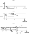
- FIG 3 is a graph of an exemplary current curve associated with the battery cell of FIG 1 while discharging the battery cell.
- FIG 4 is a graph of an exemplary voltage curve associated with the battery cell of FIG 1 while discharging the battery cell.
- an equivalent circuit model 60 used in representing an electrical response of a battery cell 12 to a flowing current is illustrated.
- One of the main elements of the equivalent circuit model 60 is the DC resistance value R0 (also referred to as an "ohmic resistance value" herein) of the resistor 80.
- R0 also referred to as an "ohmic resistance value” herein
- the voltage drop across the resistor 80 is a function of current through the resistor 80 times the resistance value of the resistor 80. This voltage drop, and associated i 2 R power loss, is power that is unavailable to the intended application of the battery cell 70.
- the ohmic resistance value R0 is at a respective lowest value.
- an exemplary current curve 250 and an exemplary voltage curve 260 are illustrated.
- a voltage drop across resistor 80 is 0 volts so the Open Circuit Voltage at the +/- terminals is effectively the same as that of the battery cell itself.
- the steps themselves are often executed at different frequencies.
- the collection of values of current may take place at one rate, such as 200 times per second (200Hz).
- the collection of values of cell voltages may take place at a different rate, such as 10Hz.
- the computation of estimations of R0 values make take place at yet another rate - for example 5Hz.
- each of the signal's values include error components due to inherent electrical noise in the hardware sensors that are used to acquire samples of current and cell voltage for each cell.
- a battery monitoring system needs to have an accurate understanding of the R0 ohmic resistance values of each battery cell in a battery pack.
- the inventor herein has recognized that in order to gain this knowledge, a battery monitoring system will frequently compute estimates of the R0 values of each battery cell and smooth the results of these estimates using a smoothing filter or slew rate limiter in order to diminish or cancel out the effects of the various types of noise-related errors in these estimates - with the assumption that the errors are basically Gaussian in nature (e.g., as likely to be inaccurately over estimating as inaccurately underestimating the R0 values).
- the inventor has conceived a battery monitoring system that identifies and selects good candidate current and cell voltage pairs for use in R0 estimate calculations, and filtering out current and cell voltage pairs that have identifiable synchronization and electrical-noise related errors, to obtain a filtered ohmic resistance value.
- the battery monitoring system includes a current sensor electrically coupled in series with a battery cell.
- the battery monitoring system further includes a voltage sensor electrically coupled in parallel to the battery cell.
- the battery monitoring system further includes a microcontroller obtaining cell current values of a cell current flowing through the battery cell from the current sensor at a first update frequency of M times per second.
- the microcontroller obtains cell voltage values of the battery cell from the voltage sensor, in parallel to the obtaining of the cell current values, with respect to electrical ground, at a second update frequency of N times per second, wherein M ⁇ N.
- the microcontroller determines a rate of change of cell current utilizing two cell current values of the cell current values. Further, at the third update frequency, the microcontroller determines a rate of change of cell voltage utilizing two cell voltage values of the cell voltage values.
- the microcontroller determines a filtered ohmic resistance value based on the rate of change of cell voltage, the rate of change of cell current, and a prior filtered ohmic resistance value, if a numerical sign of the rate of change of cell voltage being identical to a numerical sign of the rate of change of cell current, and the rate of change of cell voltage being less than or equal to an upper threshold of allowable rates of cell voltage change, and the rate of change of cell voltage being greater than or equal to a lower threshold of allowable rates of cell voltage change.
- the battery monitoring system described herein provides a substantial advantage over other systems.
- the battery monitoring system provides a technical effect of identifying and selecting good candidate current and cell voltage pairs for use in R0 estimate calculations, and filters out current and cell voltage pairs that have identifiable time synchronization and electrical-noise related errors, to obtain a filtered ohmic resistance value of the battery cell.
- FIG 1 is a schematic of a battery monitoring system for a battery cell in accordance with an exemplary embodiment.
- a battery monitoring system 10 for monitoring a battery cell 12 in accordance with an exemplary embodiment includes a battery cell 12, a current sensor 32, an electrical load 34, a voltage sensor 36, a microcontroller 42, and an external computer 43.
- An advantage of the battery monitoring system 10 is that the system 10 identifies and selects good candidate current and cell voltage pairs for use in R0 estimate calculations, and filters out current and cell voltage pairs that have identifiable time synchronization and electrical-noise related errors, to obtain a filtered ohmic resistance value of the battery cell 12.
- the battery cell 12 includes a positive terminal (+) and a negative terminal (-).
- the battery cell 12 is a pouch-type lithium-ion battery cell.
- other types of battery cells could be utilized.
- the battery cell 12 is mathematically modeled utilizing the battery cell equivalent circuit model 60 having a voltage source 70, resistors 80, 81, 82, 83, capacitors 91, 92, 93, and electrical nodes 100, 102, 104, 106.
- the resistor 80 is coupled between the voltage source 70 and the electrical node 100.
- the resistor 81 and the capacitor 91 are electrically coupled parallel to one another between the electrical nodes 100, 102.
- the resistor 82 and the capacitor 92 are electrically coupled parallel to one another between the electrical nodes 102, 104.
- the resistor 83 and the capacitor 93 are electrically coupled parallel to one another between the electrical nodes 104, 106.
- the electrical node 106 is further coupled to the voltage source 70.
- the resistor 80 has a resistance value R0 corresponding to an internal ohmic resistance value of the battery cell 12.
- the resistor 81 has a resistance value R1 corresponding to a first time-varying resistance value of the battery cell 12.
- the resistor 82 has a resistance value R2 corresponding to a second time-varying resistance value of the battery cell 12.
- the resistor 83 has a resistance value R3 corresponding to a third time-varying resistance value of the battery cell 12.
- the capacitor 91 has a capacitance value C1 corresponding to a first time-varying capacitance of the battery cell 12.
- the capacitor 92 has a capacitance value C2 corresponding to a second time-varying capacitance of the battery cell 12.
- the capacitor 93 has a capacitance value C3 corresponding to a third time-varying capacitance of the battery cell 12.
- the total steady state resistance of the battery cell equivalent circuit model 60 is R0 + R1 + R2 +R3.
- the current sensor 32 is electrically coupled in series between the positive terminal of the battery cell 12 and the electrical load 34.
- the current sensor 32 outputs current values each indicating a current level (e.g., a magnitude of current) flowing through the battery cell 32, which is received by the microcontroller 42.
- the electrical load 34 is electrically coupled between the current sensor 32 and the negative terminal of the battery cell 12.
- the electrical load is an electric motor in which the operation (e.g., speed, torque etc.) of the electric motor is controlled by the external computer 43.
- the voltage sensor 36 is electrically coupled in parallel with the electrical load 34.
- the voltage sensor 36 outputs voltage values each indicating a voltage (e.g., a magnitude of voltage) across the battery cell 12, which is received by the microcontroller 42.
- the microcontroller 42 is electrically coupled to the current sensor 32 and the voltage sensor 36.
- the microcontroller 42 operably communicates with the external computer 43 via a communication bus 44.
- the microcontroller 42 includes a memory device 130 for storing data, tables, and software instructions for implementing at least a portion of the methods described hereinafter.
- FIG 5 is a graph of current values obtained at a first update frequency, and voltage values obtained at a second update frequency, and an ohmic resistance value calculation determined at a third update frequency, in which a first pair of current values 11, 12 and first pair of voltage values V1, V2 are valid values for an ohmic resistance value calculation.
- a graph 270 of a valid pair of current values and a valid pair of voltage values for determining an accurate ohmic resistance value R0 is shown.
- the graph 270 has a plurality of current values that are obtained at a first update frequency (e.g., a current value obtained every 5 milliseconds), and a plurality of voltage values that are obtained at a second update frequency (e.g., a voltage value obtained every 100 milliseconds).
- a third update frequency e.g., an ohmic resistance value calculation obtained at greater than every 100 milliseconds.
- the current value I1 precedes the voltage value VI by a relatively small amount of time, and the current value 12 precedes the voltage value V2 by a relatively small amount of time, such that the current values 11, 12 and the voltage values V1, V2 are valid values timing wise for an ohmic resistance value calculation for R0.
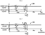
- FIG 6 is a graph of current values obtained at a first update frequency, and voltage values obtained at a second update frequency, in which a first pair of current values 13, 14 and first pair of voltage values V3, V4 are not valid values timewise for the ohmic resistance value calculation.
- a graph 280 of an invalid pair of current values and an invalid pair of voltage values that would not result in an accurate ohmic resistance value R0 is shown.
- the graph 280 has a plurality of current values that are obtained at a first update frequency (e.g., a current value obtained every 5 milliseconds), and a plurality of voltage values that are obtained at a second update frequency (e.g., a voltage value obtained every 100 milliseconds).
- the current value 13 precedes the voltage value V3 by a relatively small amount of time which is acceptable.
- the current value 14 is obtained after the voltage value V4 which would not result in an accurate ohmic resistance value R0 being calculated based on the current values 13, 14, and the voltage values V3, V4.
- FIG 7 is a graph of current values obtained at a first update frequency, and voltage values obtained at a second update frequency, in which a first pair of current values 15, 16 and first pair of voltage values V5, V6 are not valid values timewise for the ohmic resistance value calculation.
- a graph 290 of an invalid pair of current values and an invalid pair of voltage values that would not result in an accurate ohmic resistance value R0 is shown.
- the graph 290 has a plurality of current values that are obtained at a first update frequency (e.g., a current value obtained every 5 milliseconds), and a plurality of voltage values that are obtained at a second update frequency (e.g., a voltage value obtained every 100 milliseconds).
- the current value 15 precedes the voltage value V5 by a relatively small amount of time which is acceptable.
- the current value 16 is obtained a relatively large amount of time (e.g., 4.99 milliseconds) before the voltage value V6 which would not result in an accurate ohmic resistance value R0 being calculated based on the current values I5, I6, and the voltage values V5, V6.
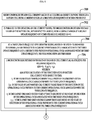
- FIGS. 1 and 8-11 a flowchart of a method for determining a filtered ohmic resistance value of a battery cell 12 will now be explained.
- FIGS. 8-11 are flowcharts of a method for determining a filtered ohmic resistance value associated with a battery cell.
- the microcontroller 42 obtains cell current values of an electrical current flowing through the battery cell 12 from the current sensor 32 at a first update frequency of M times per second.
- the microcontroller 42 obtains voltage values of the battery cell 12, with respect to ground, from the voltage sensor 36 at a second update frequency of N times per second, wherein M ⁇ N.
- I j is the value of last sampled current value prior to the execution of the current operational cycle associated with the third update frequency.
- I j-1 is the value of last sampled cell current value prior to the execution of the operational cycle previous to the current operational cycle associated with the third update frequency
- t j is the elapsed time since system startup that is recorded at the start of execution of the operational cycle associated with the third update frequency.
- t j-1 is the elapsed time since system startup that is recorded at the start of execution of the operational cycle previous to the current operational cycle associated with the third update frequency.
- V j is the value of last sampled cell voltage value prior to the execution of the operational cycle associated with the third update frequency.
- V j-1 is the value of last sampled cell voltage value prior to the execution of the operational cycle previous to the current operational cycle associated with the third update frequency.
- t j is the elapsed time since system startup that is recorded at the start of execution of the operational cycle associated with the third update frequency.
- t j-1 is the elapsed time since system startup that is recorded at the start of execution of the operational cycle previous to the current operational cycle associated with the third update frequency.
- x% is a calibrateable percentage of (abs(di/dt) ⁇ FilteredR0 j-1 )) that defines the upper threshold of acceptable dv/dt values to be selected for use in the calculation of the FilteredROj for the current operational cycle associated with the third update frequency.
- abs(di/dt) is the absolute value of rate of change of cell current from step 1(the subblock 706).
- FilteredR0 j-1 is the result of the filtered value of cell resistance R0 computed during the operational cycle previous to the current operational cycle associated with the third update frequency.
- y% is a calibrateable percentage of (abs(di/dt) ⁇ FilteredR0 j-1 )) that defines the lower threshold of acceptable dv/dt values to be selected for use in the calculation of the FilteredR0 j for the current operational cycle associated with the third update frequency.
- smoothingFilterFunction() is any recursive smoothing filter, such as a first order lag filter or single or double exponential smoothing filter, that takes as inputs a minimum the new R0 estimate, and the history of all previous R0 estimates run through the same filter function which is represented by FilteredROj-i.
- the above-described method can be at least partially embodied in the form of one or more memory devices or computer readable media having computer-executable instructions for practicing the methods.
- the memory devices can comprise one or more of the following: hard drives, RAM memory, flash memory, and other computer-readable media known to those skilled in the art; wherein, when the computer-executable instructions are loaded into and executed by one or more microcontrollers or computers, the one or more microcontrollers or computers become an apparatus programmed to practice the associated steps of the method.
- the battery monitoring system described herein provides a substantial advantage over other systems.
- the battery monitoring system provides a technical effect of identifying and selecting good candidate current and cell voltage pairs for use in R0 estimate calculations, and filters out current and cell voltage pairs that have identifiable time synchronization and electrical-noise related errors, to obtain a filtered ohmic resistance value of the battery cell.
Landscapes
- Physics & Mathematics (AREA)
- General Physics & Mathematics (AREA)
- Secondary Cells (AREA)
- Charge And Discharge Circuits For Batteries Or The Like (AREA)
- Tests Of Electric Status Of Batteries (AREA)
Abstract
Description
- The present application claims priority to
U.S. Non-Provisional Patent Application No. 16/198,955 filed on November 23, 2018 - The present disclosure relates to a battery monitoring system, and more particularly, to a battery monitoring system for estimating and determining an accurate ohmic resistance value about a battery cell.
-
FIG 2 is a schematic of a battery cell equivalent circuit model associated with the battery cell ofFIG 1 .FIG 3 is a graph of an exemplary current curve associated with the battery cell ofFIG 1 while discharging the battery cell.FIG 4 is a graph of an exemplary voltage curve associated with the battery cell ofFIG 1 while discharging the battery cell. - Referring to
FIG 2 , anequivalent circuit model 60 used in representing an electrical response of abattery cell 12 to a flowing current is illustrated. One of the main elements of theequivalent circuit model 60 is the DC resistance value R0 (also referred to as an "ohmic resistance value" herein) of theresistor 80. Pursuant to Ohm's Law, the voltage drop across theresistor 80 is a function of current through theresistor 80 times the resistance value of theresistor 80. This voltage drop, and associated i2R power loss, is power that is unavailable to the intended application of thebattery cell 70. At the beginning of life of the battery cell, the ohmic resistance value R0 is at a respective lowest value. However, aging of the battery cell, due to calendar age and current throughput, results in a growing value of RO. Thus, one of the tasks of a microcontroller is to continuously monitor/estimate the growing value of RO because of its major impact on the ability of the system to deliver power. - Estimation of RO is based on Ohm's Law, Vvoltage = Icurrent * Rresistance.
- Referring to
FIGS. 3 and 4 , an exemplarycurrent curve 250 and anexemplary voltage curve 260 are illustrated. With a value of 0 amps current at times t=0 (e.g., time =0-25 milliseconds inFIGS. 3 and 4 ), a voltage drop acrossresistor 80 is 0 volts so the Open Circuit Voltage at the +/- terminals is effectively the same as that of the battery cell itself. An instantaneous change in current at t=25 milliseconds, due to the connection of a load at the battery cell terminals at t=1 (e.g., time t=25 milliseconds inFIGS. 3 and 4 ), will cause the voltage at the terminals to drop by the value such as Icurrent × Rresistance. This value can be determined by the difference between the Open Circuit Voltage (OCV) Vt=0 and the new voltage at the terminals Vt=1. - Knowing these values, the voltage drop across
resistor 80 is equal to (Vt=1 - Vt=0) or ΔV and the value of current throughresistor 80 or It=1 then R0 can be determined as R0 = ΔV/It=1. - This form of Ohm's Law expression is a mathematically correct relationship. However, there are practical limitations to applying this in a real time embedded software system. The expression R0 = ΔV/ΔI is only ideally true for instantaneous measurements of cell voltage immediately following changes in current.
- At any amount of time Δt > 0 (after the change in the value of current I), the dynamic aspects of the Equivalent Circuit Model (R1, R2, R3, C1, C2, C3) also impact the relationship between the current I and the cell voltage measured at the terminals.
- If Δt is significant, then the relationship R0 = ΔV/ΔI is no longer valid.
- The practical difficulty in computing R0 = (Vt=(i) - Vt=(i-1)) ÷ (It=(i) - It=(i-1)), where the time Δt between the acquisition of the value Vt=(i-1) after the acquisition of the value It=(i-1) and also the time Δt between the acquisition of the value Vt=(i) after the acquisition of the value It=(i) are both at near 0 values, is the fact that the hardware and software processes involved all take non-zero amounts of time. These actual analog values of voltage and current must be acquired by the hardware, converted from analog to digital form in the hardware, the digital form of these values must be input into the computer software's domain, then these values are passed to the software processes that compute the R0 estimates.
- In addition to the non-zero amount of time involved in these steps, the steps themselves are often executed at different frequencies. The collection of values of current may take place at one rate, such as 200 times per second (200Hz). The collection of values of cell voltages may take place at a different rate, such as 10Hz. Finally, the computation of estimations of R0 values make take place at yet another rate - for example 5Hz.
- In addition to these current and cell voltage timing synchronization issues, each of the signal's values include error components due to inherent electrical noise in the hardware sensors that are used to acquire samples of current and cell voltage for each cell.
- A battery monitoring system needs to have an accurate understanding of the R0 ohmic resistance values of each battery cell in a battery pack. The inventor herein has recognized that in order to gain this knowledge, a battery monitoring system will frequently compute estimates of the R0 values of each battery cell and smooth the results of these estimates using a smoothing filter or slew rate limiter in order to diminish or cancel out the effects of the various types of noise-related errors in these estimates - with the assumption that the errors are basically Gaussian in nature (e.g., as likely to be inaccurately over estimating as inaccurately underestimating the R0 values). Further, the inventor has conceived a battery monitoring system that identifies and selects good candidate current and cell voltage pairs for use in R0 estimate calculations, and filtering out current and cell voltage pairs that have identifiable synchronization and electrical-noise related errors, to obtain a filtered ohmic resistance value.
- These and other objects and advantages of the present disclosure may be understood from the following detailed description and will become more fully apparent from the exemplary embodiments of the present disclosure. Also, it will be easily understood that the objects and advantages of the present disclosure may be realized by the means shown in the appended claims and combinations thereof.
- A battery monitoring system in accordance with an exemplary embodiment is provided. The battery monitoring system includes a current sensor electrically coupled in series with a battery cell. The battery monitoring system further includes a voltage sensor electrically coupled in parallel to the battery cell. The battery monitoring system further includes a microcontroller obtaining cell current values of a cell current flowing through the battery cell from the current sensor at a first update frequency of M times per second. The microcontroller obtains cell voltage values of the battery cell from the voltage sensor, in parallel to the obtaining of the cell current values, with respect to electrical ground, at a second update frequency of N times per second, wherein M ≥ N. At a third update frequency of R times per second, where R < M and R < N, the microcontroller determines a rate of change of cell current utilizing two cell current values of the cell current values. Further, at the third update frequency, the microcontroller determines a rate of change of cell voltage utilizing two cell voltage values of the cell voltage values. Further, at the third update frequency, the microcontroller determines a filtered ohmic resistance value based on the rate of change of cell voltage, the rate of change of cell current, and a prior filtered ohmic resistance value, if a numerical sign of the rate of change of cell voltage being identical to a numerical sign of the rate of change of cell current, and the rate of change of cell voltage being less than or equal to an upper threshold of allowable rates of cell voltage change, and the rate of change of cell voltage being greater than or equal to a lower threshold of allowable rates of cell voltage change.
- The battery monitoring system described herein provides a substantial advantage over other systems. In particular, the battery monitoring system provides a technical effect of identifying and selecting good candidate current and cell voltage pairs for use in R0 estimate calculations, and filters out current and cell voltage pairs that have identifiable time synchronization and electrical-noise related errors, to obtain a filtered ohmic resistance value of the battery cell.
- The accompanying drawings illustrate a preferred embodiment of the present disclosure and together with the foregoing disclosure, serve to provide further understanding of the technical features of the present disclosure, and thus, the present disclosure is not construed as being limited to the drawing.
-
FIG 1 is a schematic of a battery monitoring system for a battery cell in accordance with an exemplary embodiment; -
FIG 2 is a schematic of a battery cell equivalent circuit model associated with the battery cell ofFIG 1 ; -
FIG 3 is a graph of an exemplary current curve associated with the battery cell ofFIG 1 while discharging the battery cell; -
FIG 4 is a graph of an exemplary voltage curve associated with the battery cell ofFIG 1 while discharging the battery cell; -
FIG 5 is a graph of current values obtained at a first update frequency, and voltage values obtained at a second update frequency, and an ohmic resistance value calculation determined at a third update frequency, in which a first pair ofcurrent values -
FIG 6 is a graph of current values obtained at a first update frequency, and voltage values obtained at a second update frequency, in which a first pair ofcurrent values -
FIG 7 is a graph of current values obtained at a first update frequency, and voltage values obtained at a second update frequency, in which a first pair ofcurrent values -
FIGS. 8-11 are flowcharts of a method for determining a filtered ohmic resistance value associated with a battery cell. - Prior to the description, it should be understood that the terms used in the specification and the appended claims should not be construed as limited to general and dictionary meanings, but interpreted based on the meanings and concepts corresponding to technical aspects of the present disclosure on the basis of the principle that the inventor is allowed to define terms appropriately for the best explanation.
- Therefore, the description proposed herein is just a preferable example for the purpose of illustrations only, not intended to limit the scope of the disclosure, so it should be understood that other equivalents and modifications could be made thereto without departing from the scope of the disclosure.
- Additionally, in describing the present disclosure, when it is deemed that a detailed description of relevant known elements or functions renders the key subject matter of the present disclosure ambiguous, the detailed description is omitted herein.
- The terms including the ordinal number such as "first", "second" and the like, may be used to distinguish one element from another among various elements, but not intended to limit the elements by the terms.
- Throughout the specification, when a portion is referred to as "comprising" or "including" any element, it means that the portion may include other elements further, without excluding other elements, unless specifically stated otherwise.
- In addition, throughout the specification, when a portion is referred to as being "connected" to another portion, it is not limited to the case that they are "directly connected", but it also includes the case where they are "indirectly connected" with another element being interposed between them.
- Hereinafter, an apparatus according to an embodiment of the present disclosure will be described.
-
FIG 1 is a schematic of a battery monitoring system for a battery cell in accordance with an exemplary embodiment. - Referring to
FIG 1 , abattery monitoring system 10 for monitoring abattery cell 12 in accordance with an exemplary embodiment is provided. Thesystem 10 includes abattery cell 12, acurrent sensor 32, anelectrical load 34, avoltage sensor 36, amicrocontroller 42, and anexternal computer 43. An advantage of thebattery monitoring system 10 is that thesystem 10 identifies and selects good candidate current and cell voltage pairs for use in R0 estimate calculations, and filters out current and cell voltage pairs that have identifiable time synchronization and electrical-noise related errors, to obtain a filtered ohmic resistance value of thebattery cell 12. - Referring to
FIGS. 1 and 2 , thebattery cell 12 includes a positive terminal (+) and a negative terminal (-). In an exemplary embodiment, thebattery cell 12 is a pouch-type lithium-ion battery cell. Of course, in an alternative embodiment, other types of battery cells could be utilized. Thebattery cell 12 is mathematically modeled utilizing the battery cellequivalent circuit model 60 having avoltage source 70,resistors capacitors electrical nodes - The
resistor 80 is coupled between thevoltage source 70 and theelectrical node 100. Theresistor 81 and thecapacitor 91 are electrically coupled parallel to one another between theelectrical nodes resistor 82 and thecapacitor 92 are electrically coupled parallel to one another between theelectrical nodes resistor 83 and thecapacitor 93 are electrically coupled parallel to one another between theelectrical nodes electrical node 106 is further coupled to thevoltage source 70. - The
resistor 80 has a resistance value R0 corresponding to an internal ohmic resistance value of thebattery cell 12. Theresistor 81 has a resistance value R1 corresponding to a first time-varying resistance value of thebattery cell 12. Theresistor 82 has a resistance value R2 corresponding to a second time-varying resistance value of thebattery cell 12. Theresistor 83 has a resistance value R3 corresponding to a third time-varying resistance value of thebattery cell 12. Thecapacitor 91 has a capacitance value C1 corresponding to a first time-varying capacitance of thebattery cell 12. Thecapacitor 92 has a capacitance value C2 corresponding to a second time-varying capacitance of thebattery cell 12. Thecapacitor 93 has a capacitance value C3 corresponding to a third time-varying capacitance of thebattery cell 12. The total steady state resistance of the battery cellequivalent circuit model 60 is R0 + R1 + R2 +R3. - Referring to
FIG 1 , thecurrent sensor 32 is electrically coupled in series between the positive terminal of thebattery cell 12 and theelectrical load 34. Thecurrent sensor 32 outputs current values each indicating a current level (e.g., a magnitude of current) flowing through thebattery cell 32, which is received by themicrocontroller 42. - The
electrical load 34 is electrically coupled between thecurrent sensor 32 and the negative terminal of thebattery cell 12. In an exemplary embodiment, the electrical load is an electric motor in which the operation (e.g., speed, torque etc.) of the electric motor is controlled by theexternal computer 43. - The
voltage sensor 36 is electrically coupled in parallel with theelectrical load 34. Thevoltage sensor 36 outputs voltage values each indicating a voltage (e.g., a magnitude of voltage) across thebattery cell 12, which is received by themicrocontroller 42. - The
microcontroller 42 is electrically coupled to thecurrent sensor 32 and thevoltage sensor 36. Themicrocontroller 42 operably communicates with theexternal computer 43 via acommunication bus 44. Themicrocontroller 42 includes amemory device 130 for storing data, tables, and software instructions for implementing at least a portion of the methods described hereinafter. - A brief explanation of the underlying methodology for determining whether a pair of current values and a pair of voltage values are acceptable timewise for accurately determining an ohmic resistance value R0 will now be provided.
-
FIG 5 is a graph of current values obtained at a first update frequency, and voltage values obtained at a second update frequency, and an ohmic resistance value calculation determined at a third update frequency, in which a first pair ofcurrent values - Referring to
FIG 5 , agraph 270 of a valid pair of current values and a valid pair of voltage values for determining an accurate ohmic resistance value R0 is shown. In particular, thegraph 270 has a plurality of current values that are obtained at a first update frequency (e.g., a current value obtained every 5 milliseconds), and a plurality of voltage values that are obtained at a second update frequency (e.g., a voltage value obtained every 100 milliseconds). Further, an ohmic resistance value calculation for R0 is performed at a third update frequency (e.g., an ohmic resistance value calculation obtained at greater than every 100 milliseconds). The current value I1 precedes the voltage value VI by a relatively small amount of time, and thecurrent value 12 precedes the voltage value V2 by a relatively small amount of time, such that thecurrent values -
FIG 6 is a graph of current values obtained at a first update frequency, and voltage values obtained at a second update frequency, in which a first pair ofcurrent values - Referring to
FIG 6 , agraph 280 of an invalid pair of current values and an invalid pair of voltage values that would not result in an accurate ohmic resistance value R0 is shown. In particular, thegraph 280 has a plurality of current values that are obtained at a first update frequency (e.g., a current value obtained every 5 milliseconds), and a plurality of voltage values that are obtained at a second update frequency (e.g., a voltage value obtained every 100 milliseconds). Thecurrent value 13 precedes the voltage value V3 by a relatively small amount of time which is acceptable. However, thecurrent value 14 is obtained after the voltage value V4 which would not result in an accurate ohmic resistance value R0 being calculated based on thecurrent values -
FIG 7 is a graph of current values obtained at a first update frequency, and voltage values obtained at a second update frequency, in which a first pair ofcurrent values - Referring to
FIG 7 , agraph 290 of an invalid pair of current values and an invalid pair of voltage values that would not result in an accurate ohmic resistance value R0 is shown. In particular, thegraph 290 has a plurality of current values that are obtained at a first update frequency (e.g., a current value obtained every 5 milliseconds), and a plurality of voltage values that are obtained at a second update frequency (e.g., a voltage value obtained every 100 milliseconds). Thecurrent value 15 precedes the voltage value V5 by a relatively small amount of time which is acceptable. However, thecurrent value 16 is obtained a relatively large amount of time (e.g., 4.99 milliseconds) before the voltage value V6 which would not result in an accurate ohmic resistance value R0 being calculated based on the current values I5, I6, and the voltage values V5, V6. - Referring to
FIGS. 1 and8-11 , a flowchart of a method for determining a filtered ohmic resistance value of abattery cell 12 will now be explained. -
FIGS. 8-11 are flowcharts of a method for determining a filtered ohmic resistance value associated with a battery cell. - At
block 700, themicrocontroller 42 obtains cell current values of an electrical current flowing through thebattery cell 12 from thecurrent sensor 32 at a first update frequency of M times per second. - At
block 702, in parallel timewise to the obtaining of cell current values, themicrocontroller 42 obtains voltage values of thebattery cell 12, with respect to ground, from thevoltage sensor 36 at a second update frequency of N times per second, wherein M≥N. - At
block 704, at a third update frequency of R times per second, where R<M and R<N and where the symbol j is a reference to the current operational cycle associated with the third update frequency and symbol j-1 is a reference to the previous operational cycle associated with the third update frequency, the following subblocks are performed step by step. - At
subblock 706 asstep 1, themicrocontroller 42 determines the rate of change of cell current (di /dt) utilizing the following equation:
battery cell 12 current with respect to time. Ij is the value of last sampled current value prior to the execution of the current operational cycle associated with the third update frequency. Ij-1 is the value of last sampled cell current value prior to the execution of the operational cycle previous to the current operational cycle associated with the third update frequency, tj is the elapsed time since system startup that is recorded at the start of execution of the operational cycle associated with the third update frequency. tj-1 is the elapsed time since system startup that is recorded at the start of execution of the operational cycle previous to the current operational cycle associated with the third update frequency. - At
subblock 708 asstep 2, themicrocontroller 42 determines the rate of change of cell voltage (dv/dt) utilizing the following equation:
battery cell 12 voltage with respect to time. Vj is the value of last sampled cell voltage value prior to the execution of the operational cycle associated with the third update frequency. Vj-1 is the value of last sampled cell voltage value prior to the execution of the operational cycle previous to the current operational cycle associated with the third update frequency. tj is the elapsed time since system startup that is recorded at the start of execution of the operational cycle associated with the third update frequency. tj-1 is the elapsed time since system startup that is recorded at the start of execution of the operational cycle previous to the current operational cycle associated with the third update frequency. - At
subblock 710 asstep 3, themicrocontroller 42 determines the upper threshold of allowable rates of cell voltage change utilizing the following equation:
- At
subblock 712 asstep 4, themicrocontroller 42 determines the lower threshold of allowable rates of cell voltage change utilizing the following equation:
- At
subblock 714 asstep 5, themicrocontroller 42 makes a determination as to whether the (sign(dv/dt) = sign(di/dt)) AND (LowerThresholdVRofC ≤ dv/dt ≤ UpperThresholdVRofC). - If the value of the above determination of
subblock 714 is "yes", themicrocontroller 42 determines a filtered ohmic resistance value FilteredR0j utilizing the following equation:
- Alternately, if the value of the above determination of
subblock 714 is "no", themicrocontroller 42 determines the filtered ohmic resistance value FilteredR0j utilizing the following equation:
- The above-described method can be at least partially embodied in the form of one or more memory devices or computer readable media having computer-executable instructions for practicing the methods. The memory devices can comprise one or more of the following: hard drives, RAM memory, flash memory, and other computer-readable media known to those skilled in the art; wherein, when the computer-executable instructions are loaded into and executed by one or more microcontrollers or computers, the one or more microcontrollers or computers become an apparatus programmed to practice the associated steps of the method.
- The battery monitoring system described herein provides a substantial advantage over other systems. In particular, the battery monitoring system provides a technical effect of identifying and selecting good candidate current and cell voltage pairs for use in R0 estimate calculations, and filters out current and cell voltage pairs that have identifiable time synchronization and electrical-noise related errors, to obtain a filtered ohmic resistance value of the battery cell.
- While the claimed invention has been described in detail in connection with only a limited number of embodiments, it should be readily understood that the invention is not limited to such disclosed embodiments. Rather, the claimed invention can be modified to incorporate any number of variations, alterations, substitutions or equivalent arrangements not heretofore described, but which are commensurate with the spirit and scope of the invention. Additionally, while various embodiments of the claimed invention have been described, it is to be understood that aspects of the invention may include only some of the described embodiments. Accordingly, the claimed invention is not to be seen as limited by the foregoing description.
Claims (9)
- A battery monitoring system, comprising:a current sensor electrically coupled in series with a battery cell;a voltage sensor electrically coupled in parallel to the battery cell;a microcontroller obtaining cell current values of a cell current flowing through the battery cell from the current sensor at a first update frequency of M times per second;the microcontroller obtaining cell voltage values of the battery cell from the voltage sensor, in parallel to the obtaining of the cell current values, with respect to electrical ground, at a second update frequency of N times per second, wherein M is equal to and greater than N;the microcontroller determining a rate of change of cell current utilizing two cell current values of the cell current values, at a third update frequency of R times per second, where R is less than M and R is less than N;the microcontroller determining a rate of change of cell voltage utilizing two cell voltage values of the cell voltage values; andthe microcontroller determining a filtered ohmic resistance value based on the rate of change of cell voltage, the rate of change of cell current, and a prior filtered ohmic resistance value, if a numerical sign of the rate of change of cell voltage being identical to a numerical sign of the rate of change of cell current, and the rate of change of cell voltage being less than or equal to an upper threshold of allowable rates of cell voltage change, and the rate of change of cell voltage being greater than or equal to a lower threshold of allowable rates of cell voltage change.
- The battery monitoring system of claim 1, wherein:
the microcontroller determining the filtered ohmic resistance value utilizing a prior filtered ohmic resistance value, if the numerical sign of the rate of change of cell voltage is not identical to the numerical sign of the rate of change of cell current, or the rate of change of cell voltage is not less than or equal to the upper threshold of allowable rates of cell voltage change, or the rate of change of cell voltage is not greater than or equal to the lower threshold of allowable rates of cell voltage change. - The battery monitoring system of claim 1, wherein:
a symbol j is a reference to a current operational cycle associated with the third update frequency, and j-1 refers to a previous operational cycle associated with the third update frequency. - The battery monitoring system of claim 3, wherein:
the microcontroller determining the rate of change of cell current utilizing a following equation:
- The battery monitoring system of claim 3, wherein:
the microcontroller determining the rate of change of cell voltage utilizing a following equation:
- The battery monitoring system of claim 3, wherein:
the microcontroller determining the upper threshold of allowable rates of cell voltage change utilizing a following equation:
- The battery monitoring system of claim 3, wherein:
the microcontroller determining the lower threshold of allowable rates of cell voltage change utilizing a following equation:
- The battery monitoring system of claim 3, wherein:
the microcontroller determining the filtered ohmic resistance value if the numerical sign of the rate of change of cell voltage is identical to the numerical sign of the rate of change of cell current, and the rate of change of cell voltage is less than or equal to the upper threshold of allowable rates of cell voltage change, and the rate of change of cell voltage is greater than or equal to the lower threshold of allowable rates of cell voltage change, utilizing a following equation:
- The battery monitoring system of claim 8, wherein:
the recursive smoothing filter is a first order lag filter, or a single exponential smoothing filter, or a double exponential smoothing filter.
Applications Claiming Priority (2)
| Application Number | Priority Date | Filing Date | Title |
|---|---|---|---|
| US16/198,955 US10948547B2 (en) | 2018-11-23 | 2018-11-23 | Battery monitoring system |
| PCT/KR2019/015895 WO2020106043A1 (en) | 2018-11-23 | 2019-11-19 | Battery monitoring system |
Publications (3)
| Publication Number | Publication Date |
|---|---|
| EP3761048A1 true EP3761048A1 (en) | 2021-01-06 |
| EP3761048A4 EP3761048A4 (en) | 2021-06-23 |
| EP3761048B1 EP3761048B1 (en) | 2022-03-23 |
Family
ID=70770682
Family Applications (1)
| Application Number | Title | Priority Date | Filing Date |
|---|---|---|---|
| EP19886649.3A Active EP3761048B1 (en) | 2018-11-23 | 2019-11-19 | Battery monitoring system |
Country Status (6)
| Country | Link |
|---|---|
| US (1) | US10948547B2 (en) |
| EP (1) | EP3761048B1 (en) |
| JP (1) | JP7014491B2 (en) |
| KR (1) | KR102882637B1 (en) |
| CN (1) | CN111989581B (en) |
| WO (1) | WO2020106043A1 (en) |
Families Citing this family (5)
| Publication number | Priority date | Publication date | Assignee | Title |
|---|---|---|---|---|
| KR102253781B1 (en) * | 2017-04-28 | 2021-05-20 | 주식회사 엘지화학 | Apparatus and method for controlling discharge |
| KR102864288B1 (en) * | 2020-11-26 | 2025-09-26 | 에스케이온 주식회사 | Apparatus and method to synchronize state information of battery |
| KR102796970B1 (en) * | 2022-05-03 | 2025-04-18 | 주식회사 에이젠글로벌 | Method for monitoring e-mobility battery value and apparatus for performing the method |
| EP4700409A1 (en) * | 2023-04-19 | 2026-02-25 | Vehicle Energy Japan Inc. | Battery control device and vehicle control device |
| FR3161036A1 (en) * | 2024-04-04 | 2025-10-10 | Electricite De France | Method and system for monitoring a battery by tracking its voltage and current |
Family Cites Families (29)
| Publication number | Priority date | Publication date | Assignee | Title |
|---|---|---|---|---|
| US20030206021A1 (en) * | 1997-07-25 | 2003-11-06 | Laletin William H. | Method and apparatus for measuring and analyzing electrical or electrochemical systems |
| US6087808A (en) * | 1999-04-23 | 2000-07-11 | Pritchard; Jeffrey A. | System and method for accurately determining remaining battery life |
| WO2002071087A1 (en) * | 2001-03-08 | 2002-09-12 | Daimlerchrysler Ag | Method and system for determining the buffer action of a battery |
| US6620538B2 (en) | 2002-01-23 | 2003-09-16 | Avista Laboratories, Inc. | Method and apparatus for monitoring equivalent series resistance and for shunting a fuel cell |
| JP4043977B2 (en) | 2003-03-11 | 2008-02-06 | 株式会社日本自動車部品総合研究所 | Secondary battery internal resistance detection device and internal resistance detection method |
| EP2626716B1 (en) | 2003-06-27 | 2015-09-16 | The Furukawa Electric Co., Ltd. | Device and method for judging deterioration of accumulator / secondary cell |
| CN101639523B (en) | 2003-06-27 | 2011-07-27 | 古河电气工业株式会社 | Method and device for measuring internal impedance of secondary battery, method and device for determining deterioration, and power supply system |
| US7795874B1 (en) * | 2007-10-10 | 2010-09-14 | Commissariat A L'energie Atomique | Method of estimation of the state of charge of a lead-acid battery |
| JP4925060B2 (en) * | 2007-10-19 | 2012-04-25 | 本田技研工業株式会社 | Battery state estimation device |
| PL2365350T3 (en) * | 2008-11-10 | 2020-06-29 | Lg Chem, Ltd. | Apparatus and method for measuring current and voltage of secondary battery pack in synchronization manner |
| JP5334697B2 (en) | 2009-06-15 | 2013-11-06 | 本田技研工業株式会社 | Battery state estimation device |
| JP2011047820A (en) | 2009-08-27 | 2011-03-10 | Toshiba Corp | Secondary cell device and vehicle |
| JP2011106952A (en) * | 2009-11-17 | 2011-06-02 | Honda Motor Co Ltd | Method for estimating residual capacity of battery |
| JP5381664B2 (en) * | 2009-12-02 | 2014-01-08 | トヨタ自動車株式会社 | Abnormality detection device for battery pack |
| JP2011257219A (en) * | 2010-06-08 | 2011-12-22 | Nissan Motor Co Ltd | Internal resistance of secondary battery and calculation device for calculating open voltage |
| JP5558941B2 (en) * | 2010-06-30 | 2014-07-23 | 三洋電機株式会社 | How to detect battery internal resistance |
| EP2761317A2 (en) * | 2011-09-30 | 2014-08-06 | KPIT Technologies Limited | A system and method for determining state of charge of a battery |
| WO2013046714A1 (en) * | 2011-09-30 | 2013-04-04 | パナソニック株式会社 | Internal resistance detecting circuit and battery power supply apparatus |
| KR101863036B1 (en) | 2011-11-30 | 2018-06-01 | 주식회사 실리콘웍스 | Method for estimating the state of charge of battery and battery management system |
| KR101498764B1 (en) * | 2012-05-10 | 2015-03-04 | 주식회사 엘지화학 | Method and apparatus for battery resistance estimation, and battery management system using the same |
| JP2013246088A (en) | 2012-05-28 | 2013-12-09 | Toyota Industries Corp | Method and device for estimating internal resistance of battery |
| DE102012209660A1 (en) | 2012-06-08 | 2013-12-12 | Robert Bosch Gmbh | Battery system and associated method for determining the internal resistance of battery cells or battery modules of the battery system |
| US20140266228A1 (en) * | 2013-03-15 | 2014-09-18 | Qualcomm Incorporated | Active measurement of battery equivalent series resistance |
| DE102014205495A1 (en) * | 2014-03-25 | 2015-10-01 | Robert Bosch Gmbh | Electronic battery sensor and method for determining an internal resistance of a battery |
| US9707855B1 (en) * | 2016-04-15 | 2017-07-18 | Ford Global Technologies, Llc | Battery overcurrent diagnostic system |
| CN105954592B (en) | 2016-07-18 | 2017-08-25 | 天津金星奥宇科技有限公司 | A kind of power battery pack internal resistance measurement system |
| US10436851B2 (en) * | 2016-07-29 | 2019-10-08 | Con Edison Battery Storage, Llc | Electrical energy storage system with battery resistance estimation |
| CN108226787A (en) * | 2017-08-08 | 2018-06-29 | 河南航天液压气动技术有限公司 | Internal resistance of cell detection method and detection device |
| CN107907834B (en) * | 2017-10-25 | 2020-08-07 | 广州市香港科大霍英东研究院 | A current drift correction method, system and device for a battery management system |
-
2018
- 2018-11-23 US US16/198,955 patent/US10948547B2/en active Active
-
2019
- 2019-11-19 KR KR1020207013891A patent/KR102882637B1/en active Active
- 2019-11-19 CN CN201980022217.3A patent/CN111989581B/en active Active
- 2019-11-19 WO PCT/KR2019/015895 patent/WO2020106043A1/en not_active Ceased
- 2019-11-19 JP JP2020539062A patent/JP7014491B2/en active Active
- 2019-11-19 EP EP19886649.3A patent/EP3761048B1/en active Active
Also Published As
| Publication number | Publication date |
|---|---|
| KR102882637B1 (en) | 2025-11-05 |
| JP2021512451A (en) | 2021-05-13 |
| US10948547B2 (en) | 2021-03-16 |
| WO2020106043A1 (en) | 2020-05-28 |
| US20200166579A1 (en) | 2020-05-28 |
| CN111989581B (en) | 2023-06-06 |
| KR20210082124A (en) | 2021-07-02 |
| JP7014491B2 (en) | 2022-02-01 |
| EP3761048B1 (en) | 2022-03-23 |
| CN111989581A (en) | 2020-11-24 |
| EP3761048A4 (en) | 2021-06-23 |
Similar Documents
| Publication | Publication Date | Title |
|---|---|---|
| EP3761048A1 (en) | Battery monitoring system | |
| EP3623829B1 (en) | Apparatus and method for estimating state of charge of secondary battery | |
| JP5946436B2 (en) | Battery parameter estimation apparatus and parameter estimation method | |
| EP2765436A1 (en) | Battery state-of-charge estimation device and state-of-charge estimation method | |
| CN105026944B (en) | Secondary battery state detection device and secondary battery state detection method | |
| EP3011350B1 (en) | Monitoring charge stored in a battery | |
| KR102022426B1 (en) | Estimating the state of charge of a battery | |
| JP2016090330A (en) | Battery parameter estimation device | |
| CN109633276B (en) | Insulation resistance detection method and device based on full-bridge insulation detection circuit | |
| JP6253137B2 (en) | Battery state estimation device for secondary battery | |
| JP2010508507A (en) | Apparatus and method for determining the state of charge of a battery when the battery is not in equilibrium | |
| JP2015052482A (en) | Soundness estimation device and soundness estimation method for battery | |
| EP2761317A2 (en) | A system and method for determining state of charge of a battery | |
| JP6450565B2 (en) | Battery parameter estimation device | |
| WO2018172216A1 (en) | Battery energy store | |
| CN108931732A (en) | Method for estimating the electric current and state-of-charge of battery pack or battery unit | |
| WO2023225243A1 (en) | Apparatus and method for battery soh estimation, method for forming a 2d-lut thereof | |
| CN105527492B (en) | Method and apparatus for determining resistance change of energy storage device and automobile | |
| US20170089985A1 (en) | Method for estimating an electrical capacitance of a secondary battery | |
| KR20170059741A (en) | System and method for diagnosing dc input capacitor of inverter, and a recording medium having computer readable program for executing the method | |
| EP3853625B1 (en) | A method and system for estimating the state-of-health of a battery | |
| CN113009363A (en) | Method and apparatus for measuring ohmic resistance of battery | |
| CN114019396B (en) | A battery pack impedance detection method and device | |
| EP4390416A1 (en) | Capacity and state-of-charge estimation for a multi-battery energy storage system | |
| CN121586851A (en) | Battery diagnosis device and battery diagnosis method |
Legal Events
| Date | Code | Title | Description |
|---|---|---|---|
| STAA | Information on the status of an ep patent application or granted ep patent |
Free format text: STATUS: THE INTERNATIONAL PUBLICATION HAS BEEN MADE |
|
| PUAI | Public reference made under article 153(3) epc to a published international application that has entered the european phase |
Free format text: ORIGINAL CODE: 0009012 |
|
| STAA | Information on the status of an ep patent application or granted ep patent |
Free format text: STATUS: REQUEST FOR EXAMINATION WAS MADE |
|
| 17P | Request for examination filed |
Effective date: 20200930 |
|
| AK | Designated contracting states |
Kind code of ref document: A1 Designated state(s): AL AT BE BG CH CY CZ DE DK EE ES FI FR GB GR HR HU IE IS IT LI LT LU LV MC MK MT NL NO PL PT RO RS SE SI SK SM TR |
|
| AX | Request for extension of the european patent |
Extension state: BA ME |
|
| A4 | Supplementary search report drawn up and despatched |
Effective date: 20210525 |
|
| RIC1 | Information provided on ipc code assigned before grant |
Ipc: G01R 31/36 20200101AFI20210518BHEP Ipc: G01R 31/3842 20190101ALI20210518BHEP Ipc: G01R 31/389 20190101ALI20210518BHEP |
|
| GRAP | Despatch of communication of intention to grant a patent |
Free format text: ORIGINAL CODE: EPIDOSNIGR1 |
|
| STAA | Information on the status of an ep patent application or granted ep patent |
Free format text: STATUS: GRANT OF PATENT IS INTENDED |
|
| DAV | Request for validation of the european patent (deleted) | ||
| DAX | Request for extension of the european patent (deleted) | ||
| INTG | Intention to grant announced |
Effective date: 20211217 |
|
| RAP1 | Party data changed (applicant data changed or rights of an application transferred) |
Owner name: LG ENERGY SOLUTION LTD. |
|
| GRAS | Grant fee paid |
Free format text: ORIGINAL CODE: EPIDOSNIGR3 |
|
| GRAA | (expected) grant |
Free format text: ORIGINAL CODE: 0009210 |
|
| STAA | Information on the status of an ep patent application or granted ep patent |
Free format text: STATUS: THE PATENT HAS BEEN GRANTED |
|
| AK | Designated contracting states |
Kind code of ref document: B1 Designated state(s): AL AT BE BG CH CY CZ DE DK EE ES FI FR GB GR HR HU IE IS IT LI LT LU LV MC MK MT NL NO PL PT RO RS SE SI SK SM TR |
|
| REG | Reference to a national code |
Ref country code: GB Ref legal event code: FG4D |
|
| RAP4 | Party data changed (patent owner data changed or rights of a patent transferred) |
Owner name: LG ENERGY SOLUTION, LTD. |
|
| REG | Reference to a national code |
Ref country code: CH Ref legal event code: EP |
|
| REG | Reference to a national code |
Ref country code: DE Ref legal event code: R096 Ref document number: 602019012900 Country of ref document: DE |
|
| REG | Reference to a national code |
Ref country code: IE Ref legal event code: FG4D |
|
| REG | Reference to a national code |
Ref country code: AT Ref legal event code: REF Ref document number: 1477802 Country of ref document: AT Kind code of ref document: T Effective date: 20220415 |
|
| REG | Reference to a national code |
Ref country code: LT Ref legal event code: MG9D |
|
| REG | Reference to a national code |
Ref country code: NL Ref legal event code: MP Effective date: 20220323 |
|
| PG25 | Lapsed in a contracting state [announced via postgrant information from national office to epo] |
Ref country code: SE Free format text: LAPSE BECAUSE OF FAILURE TO SUBMIT A TRANSLATION OF THE DESCRIPTION OR TO PAY THE FEE WITHIN THE PRESCRIBED TIME-LIMIT Effective date: 20220323 Ref country code: RS Free format text: LAPSE BECAUSE OF FAILURE TO SUBMIT A TRANSLATION OF THE DESCRIPTION OR TO PAY THE FEE WITHIN THE PRESCRIBED TIME-LIMIT Effective date: 20220323 Ref country code: NO Free format text: LAPSE BECAUSE OF FAILURE TO SUBMIT A TRANSLATION OF THE DESCRIPTION OR TO PAY THE FEE WITHIN THE PRESCRIBED TIME-LIMIT Effective date: 20220623 Ref country code: LT Free format text: LAPSE BECAUSE OF FAILURE TO SUBMIT A TRANSLATION OF THE DESCRIPTION OR TO PAY THE FEE WITHIN THE PRESCRIBED TIME-LIMIT Effective date: 20220323 Ref country code: HR Free format text: LAPSE BECAUSE OF FAILURE TO SUBMIT A TRANSLATION OF THE DESCRIPTION OR TO PAY THE FEE WITHIN THE PRESCRIBED TIME-LIMIT Effective date: 20220323 Ref country code: BG Free format text: LAPSE BECAUSE OF FAILURE TO SUBMIT A TRANSLATION OF THE DESCRIPTION OR TO PAY THE FEE WITHIN THE PRESCRIBED TIME-LIMIT Effective date: 20220623 |
|
| REG | Reference to a national code |
Ref country code: AT Ref legal event code: MK05 Ref document number: 1477802 Country of ref document: AT Kind code of ref document: T Effective date: 20220323 |
|
| PG25 | Lapsed in a contracting state [announced via postgrant information from national office to epo] |
Ref country code: LV Free format text: LAPSE BECAUSE OF FAILURE TO SUBMIT A TRANSLATION OF THE DESCRIPTION OR TO PAY THE FEE WITHIN THE PRESCRIBED TIME-LIMIT Effective date: 20220323 Ref country code: GR Free format text: LAPSE BECAUSE OF FAILURE TO SUBMIT A TRANSLATION OF THE DESCRIPTION OR TO PAY THE FEE WITHIN THE PRESCRIBED TIME-LIMIT Effective date: 20220624 Ref country code: FI Free format text: LAPSE BECAUSE OF FAILURE TO SUBMIT A TRANSLATION OF THE DESCRIPTION OR TO PAY THE FEE WITHIN THE PRESCRIBED TIME-LIMIT Effective date: 20220323 |
|
| PG25 | Lapsed in a contracting state [announced via postgrant information from national office to epo] |
Ref country code: NL Free format text: LAPSE BECAUSE OF FAILURE TO SUBMIT A TRANSLATION OF THE DESCRIPTION OR TO PAY THE FEE WITHIN THE PRESCRIBED TIME-LIMIT Effective date: 20220323 |
|
| PG25 | Lapsed in a contracting state [announced via postgrant information from national office to epo] |
Ref country code: SM Free format text: LAPSE BECAUSE OF FAILURE TO SUBMIT A TRANSLATION OF THE DESCRIPTION OR TO PAY THE FEE WITHIN THE PRESCRIBED TIME-LIMIT Effective date: 20220323 Ref country code: SK Free format text: LAPSE BECAUSE OF FAILURE TO SUBMIT A TRANSLATION OF THE DESCRIPTION OR TO PAY THE FEE WITHIN THE PRESCRIBED TIME-LIMIT Effective date: 20220323 Ref country code: RO Free format text: LAPSE BECAUSE OF FAILURE TO SUBMIT A TRANSLATION OF THE DESCRIPTION OR TO PAY THE FEE WITHIN THE PRESCRIBED TIME-LIMIT Effective date: 20220323 Ref country code: PT Free format text: LAPSE BECAUSE OF FAILURE TO SUBMIT A TRANSLATION OF THE DESCRIPTION OR TO PAY THE FEE WITHIN THE PRESCRIBED TIME-LIMIT Effective date: 20220725 Ref country code: ES Free format text: LAPSE BECAUSE OF FAILURE TO SUBMIT A TRANSLATION OF THE DESCRIPTION OR TO PAY THE FEE WITHIN THE PRESCRIBED TIME-LIMIT Effective date: 20220323 Ref country code: EE Free format text: LAPSE BECAUSE OF FAILURE TO SUBMIT A TRANSLATION OF THE DESCRIPTION OR TO PAY THE FEE WITHIN THE PRESCRIBED TIME-LIMIT Effective date: 20220323 Ref country code: CZ Free format text: LAPSE BECAUSE OF FAILURE TO SUBMIT A TRANSLATION OF THE DESCRIPTION OR TO PAY THE FEE WITHIN THE PRESCRIBED TIME-LIMIT Effective date: 20220323 Ref country code: AT Free format text: LAPSE BECAUSE OF FAILURE TO SUBMIT A TRANSLATION OF THE DESCRIPTION OR TO PAY THE FEE WITHIN THE PRESCRIBED TIME-LIMIT Effective date: 20220323 |
|
| PG25 | Lapsed in a contracting state [announced via postgrant information from national office to epo] |
Ref country code: PL Free format text: LAPSE BECAUSE OF FAILURE TO SUBMIT A TRANSLATION OF THE DESCRIPTION OR TO PAY THE FEE WITHIN THE PRESCRIBED TIME-LIMIT Effective date: 20220323 Ref country code: IS Free format text: LAPSE BECAUSE OF FAILURE TO SUBMIT A TRANSLATION OF THE DESCRIPTION OR TO PAY THE FEE WITHIN THE PRESCRIBED TIME-LIMIT Effective date: 20220723 Ref country code: AL Free format text: LAPSE BECAUSE OF FAILURE TO SUBMIT A TRANSLATION OF THE DESCRIPTION OR TO PAY THE FEE WITHIN THE PRESCRIBED TIME-LIMIT Effective date: 20220323 |
|
| REG | Reference to a national code |
Ref country code: DE Ref legal event code: R097 Ref document number: 602019012900 Country of ref document: DE |
|
| PLBE | No opposition filed within time limit |
Free format text: ORIGINAL CODE: 0009261 |
|
| STAA | Information on the status of an ep patent application or granted ep patent |
Free format text: STATUS: NO OPPOSITION FILED WITHIN TIME LIMIT |
|
| PG25 | Lapsed in a contracting state [announced via postgrant information from national office to epo] |
Ref country code: DK Free format text: LAPSE BECAUSE OF FAILURE TO SUBMIT A TRANSLATION OF THE DESCRIPTION OR TO PAY THE FEE WITHIN THE PRESCRIBED TIME-LIMIT Effective date: 20220323 |
|
| 26N | No opposition filed |
Effective date: 20230102 |
|
| PG25 | Lapsed in a contracting state [announced via postgrant information from national office to epo] |
Ref country code: SI Free format text: LAPSE BECAUSE OF FAILURE TO SUBMIT A TRANSLATION OF THE DESCRIPTION OR TO PAY THE FEE WITHIN THE PRESCRIBED TIME-LIMIT Effective date: 20220323 |
|
| P01 | Opt-out of the competence of the unified patent court (upc) registered |
Effective date: 20230408 |
|
| PG25 | Lapsed in a contracting state [announced via postgrant information from national office to epo] |
Ref country code: MC Free format text: LAPSE BECAUSE OF FAILURE TO SUBMIT A TRANSLATION OF THE DESCRIPTION OR TO PAY THE FEE WITHIN THE PRESCRIBED TIME-LIMIT Effective date: 20220323 |
|
| REG | Reference to a national code |
Ref country code: CH Ref legal event code: PL |
|
| REG | Reference to a national code |
Ref country code: BE Ref legal event code: MM Effective date: 20221130 |
|
| PG25 | Lapsed in a contracting state [announced via postgrant information from national office to epo] |
Ref country code: LI Free format text: LAPSE BECAUSE OF NON-PAYMENT OF DUE FEES Effective date: 20221130 Ref country code: IT Free format text: LAPSE BECAUSE OF FAILURE TO SUBMIT A TRANSLATION OF THE DESCRIPTION OR TO PAY THE FEE WITHIN THE PRESCRIBED TIME-LIMIT Effective date: 20220323 Ref country code: CH Free format text: LAPSE BECAUSE OF NON-PAYMENT OF DUE FEES Effective date: 20221130 |
|
| PG25 | Lapsed in a contracting state [announced via postgrant information from national office to epo] |
Ref country code: LU Free format text: LAPSE BECAUSE OF NON-PAYMENT OF DUE FEES Effective date: 20221119 |
|
| PG25 | Lapsed in a contracting state [announced via postgrant information from national office to epo] |
Ref country code: IE Free format text: LAPSE BECAUSE OF NON-PAYMENT OF DUE FEES Effective date: 20221119 |
|
| PG25 | Lapsed in a contracting state [announced via postgrant information from national office to epo] |
Ref country code: BE Free format text: LAPSE BECAUSE OF NON-PAYMENT OF DUE FEES Effective date: 20221130 |
|
| PG25 | Lapsed in a contracting state [announced via postgrant information from national office to epo] |
Ref country code: CY Free format text: LAPSE BECAUSE OF FAILURE TO SUBMIT A TRANSLATION OF THE DESCRIPTION OR TO PAY THE FEE WITHIN THE PRESCRIBED TIME-LIMIT Effective date: 20220323 |
|
| PG25 | Lapsed in a contracting state [announced via postgrant information from national office to epo] |
Ref country code: MK Free format text: LAPSE BECAUSE OF FAILURE TO SUBMIT A TRANSLATION OF THE DESCRIPTION OR TO PAY THE FEE WITHIN THE PRESCRIBED TIME-LIMIT Effective date: 20220323 Ref country code: HU Free format text: LAPSE BECAUSE OF FAILURE TO SUBMIT A TRANSLATION OF THE DESCRIPTION OR TO PAY THE FEE WITHIN THE PRESCRIBED TIME-LIMIT; INVALID AB INITIO Effective date: 20191119 |
|
| PG25 | Lapsed in a contracting state [announced via postgrant information from national office to epo] |
Ref country code: TR Free format text: LAPSE BECAUSE OF FAILURE TO SUBMIT A TRANSLATION OF THE DESCRIPTION OR TO PAY THE FEE WITHIN THE PRESCRIBED TIME-LIMIT Effective date: 20220323 |
|
| PG25 | Lapsed in a contracting state [announced via postgrant information from national office to epo] |
Ref country code: MT Free format text: LAPSE BECAUSE OF FAILURE TO SUBMIT A TRANSLATION OF THE DESCRIPTION OR TO PAY THE FEE WITHIN THE PRESCRIBED TIME-LIMIT Effective date: 20220323 |
|
| PGFP | Annual fee paid to national office [announced via postgrant information from national office to epo] |
Ref country code: DE Payment date: 20251020 Year of fee payment: 7 |
|
| PGFP | Annual fee paid to national office [announced via postgrant information from national office to epo] |
Ref country code: GB Payment date: 20251023 Year of fee payment: 7 |
|
| PGFP | Annual fee paid to national office [announced via postgrant information from national office to epo] |
Ref country code: FR Payment date: 20251021 Year of fee payment: 7 |