EP3759818B1 - Schaltbare differenzialkondensatoren für hochfrequenzleistungsverstärker - Google Patents
Schaltbare differenzialkondensatoren für hochfrequenzleistungsverstärker Download PDFInfo
- Publication number
- EP3759818B1 EP3759818B1 EP19920624.4A EP19920624A EP3759818B1 EP 3759818 B1 EP3759818 B1 EP 3759818B1 EP 19920624 A EP19920624 A EP 19920624A EP 3759818 B1 EP3759818 B1 EP 3759818B1
- Authority
- EP
- European Patent Office
- Prior art keywords
- ccs
- capacitor
- node
- negative
- positive
- Prior art date
- Legal status (The legal status is an assumption and is not a legal conclusion. Google has not performed a legal analysis and makes no representation as to the accuracy of the status listed.)
- Active
Links
Images



Classifications
-
- H—ELECTRICITY
- H03—ELECTRONIC CIRCUITRY
- H03J—TUNING RESONANT CIRCUITS; SELECTING RESONANT CIRCUITS
- H03J3/00—Continuous tuning
- H03J3/24—Continuous tuning of more than one resonant circuit simultaneously, the circuits being tuned to substantially the same frequency, e.g. for single-knob tuning
-
- H—ELECTRICITY
- H03—ELECTRONIC CIRCUITRY
- H03F—AMPLIFIERS
- H03F3/00—Amplifiers with only discharge tubes or only semiconductor devices as amplifying elements
- H03F3/20—Power amplifiers, e.g. Class B amplifiers, Class C amplifiers
-
- H—ELECTRICITY
- H03—ELECTRONIC CIRCUITRY
- H03B—GENERATION OF OSCILLATIONS, DIRECTLY OR BY FREQUENCY-CHANGING, BY CIRCUITS EMPLOYING ACTIVE ELEMENTS WHICH OPERATE IN A NON-SWITCHING MANNER; GENERATION OF NOISE BY SUCH CIRCUITS
- H03B5/00—Generation of oscillations using amplifier with regenerative feedback from output to input
- H03B5/08—Generation of oscillations using amplifier with regenerative feedback from output to input with frequency-determining element comprising lumped inductance and capacitance
- H03B5/12—Generation of oscillations using amplifier with regenerative feedback from output to input with frequency-determining element comprising lumped inductance and capacitance active element in amplifier being semiconductor device
- H03B5/1237—Generation of oscillations using amplifier with regenerative feedback from output to input with frequency-determining element comprising lumped inductance and capacitance active element in amplifier being semiconductor device comprising means for varying the frequency of the generator
- H03B5/1262—Generation of oscillations using amplifier with regenerative feedback from output to input with frequency-determining element comprising lumped inductance and capacitance active element in amplifier being semiconductor device comprising means for varying the frequency of the generator the means comprising switched elements
- H03B5/1265—Generation of oscillations using amplifier with regenerative feedback from output to input with frequency-determining element comprising lumped inductance and capacitance active element in amplifier being semiconductor device comprising means for varying the frequency of the generator the means comprising switched elements switched capacitors
-
- H—ELECTRICITY
- H03—ELECTRONIC CIRCUITRY
- H03F—AMPLIFIERS
- H03F1/00—Details of amplifiers with only discharge tubes, only semiconductor devices or only unspecified devices as amplifying elements
- H03F1/56—Modifications of input or output impedances, not otherwise provided for
- H03F1/565—Modifications of input or output impedances, not otherwise provided for using inductive elements
-
- H—ELECTRICITY
- H03—ELECTRONIC CIRCUITRY
- H03F—AMPLIFIERS
- H03F3/00—Amplifiers with only discharge tubes or only semiconductor devices as amplifying elements
- H03F3/189—High-frequency amplifiers, e.g. radio frequency amplifiers
-
- H—ELECTRICITY
- H03—ELECTRONIC CIRCUITRY
- H03F—AMPLIFIERS
- H03F3/00—Amplifiers with only discharge tubes or only semiconductor devices as amplifying elements
- H03F3/189—High-frequency amplifiers, e.g. radio frequency amplifiers
- H03F3/19—High-frequency amplifiers, e.g. radio frequency amplifiers with semiconductor devices only
- H03F3/191—Tuned amplifiers
-
- H—ELECTRICITY
- H03—ELECTRONIC CIRCUITRY
- H03F—AMPLIFIERS
- H03F3/00—Amplifiers with only discharge tubes or only semiconductor devices as amplifying elements
- H03F3/189—High-frequency amplifiers, e.g. radio frequency amplifiers
- H03F3/19—High-frequency amplifiers, e.g. radio frequency amplifiers with semiconductor devices only
- H03F3/193—High-frequency amplifiers, e.g. radio frequency amplifiers with semiconductor devices only with field-effect devices
-
- H—ELECTRICITY
- H03—ELECTRONIC CIRCUITRY
- H03J—TUNING RESONANT CIRCUITS; SELECTING RESONANT CIRCUITS
- H03J3/00—Continuous tuning
- H03J3/20—Continuous tuning of single resonant circuit by varying inductance only or capacitance only
-
- H—ELECTRICITY
- H03—ELECTRONIC CIRCUITRY
- H03J—TUNING RESONANT CIRCUITS; SELECTING RESONANT CIRCUITS
- H03J3/00—Continuous tuning
- H03J3/28—Continuous tuning of more than one resonant circuit simultaneously, the tuning frequencies of the circuits having a substantially constant difference throughout the tuning range
- H03J3/32—Arrangements for ensuring tracking with variable capacitors
-
- H—ELECTRICITY
- H03—ELECTRONIC CIRCUITRY
- H03F—AMPLIFIERS
- H03F2200/00—Indexing scheme relating to amplifiers
- H03F2200/387—A circuit being added at the output of an amplifier to adapt the output impedance of the amplifier
-
- H—ELECTRICITY
- H03—ELECTRONIC CIRCUITRY
- H03F—AMPLIFIERS
- H03F2200/00—Indexing scheme relating to amplifiers
- H03F2200/451—Indexing scheme relating to amplifiers the amplifier being a radio frequency amplifier
-
- H—ELECTRICITY
- H03—ELECTRONIC CIRCUITRY
- H03F—AMPLIFIERS
- H03F2200/00—Indexing scheme relating to amplifiers
- H03F2200/546—A tunable capacitance being present in an amplifier circuit
-
- H—ELECTRICITY
- H03—ELECTRONIC CIRCUITRY
- H03J—TUNING RESONANT CIRCUITS; SELECTING RESONANT CIRCUITS
- H03J2200/00—Indexing scheme relating to tuning resonant circuits and selecting resonant circuits
- H03J2200/10—Tuning of a resonator by means of digitally controlled capacitor bank
Definitions
- the application relates generally to radiofrequency transceivers. More particularly, embodiments relate to differential switchable capacitors for use in tuning resonant networks of radiofrequency power amplifiers.
- transceiver circuits e.g., transmitter circuits and/or receiver circuits.
- the transceiver circuits can include radiofrequency power amplifiers and resonant networks.
- the power amplifiers can add a desirable amount of gain to a signal, and the resonant networks can be used to tune the output of the power amplifier to a desired frequency.
- a capacitor and inductor can be used as a resonating circuit, and the values of the capacitor and inductor can effectively define the frequency of the resonating circuit.
- a transceiver circuit may be designed to selectively operate in different types of networks (e.g., for different companies, different countries, etc.). Re-tuning the transceiver can involve using a tunable resonant circuit.
- Such circuits can be designed with multiple capacitors that can be selectively coupled with a single inductor, so that selecting a particular capacitor can effectively select a particular resonant frequency for the circuit.
- the switch When the switch is ON (i.e., the capacitor is being used in the resonant circuit), the switch may see only a relatively small voltage swing. However, when the switch is OFF (i.e., the capacitor is not being used), the full output voltage swing from the power amplifier may be transferred to the switch.
- the switch is conventionally implemented as a typical transistor (e.g., a complementary metal-oxide semiconductor, CMOS, transistor), which can have a relatively low stress voltage. As such, when the switch is OFF, the large voltage swing can cause degradation of the transistor and/or other undesirable conditions.
- CMOS complementary metal-oxide semiconductor
- Some conventional applications simply avoid such concerns by selecting a single capacitor, such that the resonant circuit is not tunable.
- Other conventional approaches use one or more off-chip capacitors, which can be selectively coupled into the circuit, for example, by selectively hard-wiring a particular one of the capacitors to the circuit, by using a physical switch component (e.g., a dip switch), etc.
- US 2016373058 A1 discloses a circuit for an oscillator with common-mode resonance.
- US 2005174184 A1 discloses a VCO with temperature compensation.
- US 2003171109 A1 discloses an integrated center frequency selectable resonant coupling network suited for use in an integrated circuit.
- Embodiments provide circuits, devices, and methods for tuning a resonant circuit using differential switchable capacitors.
- embodiments can operate in context of a power amplifier with a tunable resonant output network.
- To tune the network multiple differential switchable capacitors are provided in parallel.
- FIG. 1 shows a block diagram of an illustrative radiofrequency transceiver power amplifier circuit 100 for use with embodiments described herein.
- the illustrative transceiver power amplifier circuit 100 includes a power amplifier 110, a resonant circuit 130, and a matching network 120 coupled with a load (illustrated as load resistor 122).
- Embodiments of the power amplifier 110 operate to add gain to an input signal 102, thereby generating an amplified output signal at node "A".
- Embodiments of the matching network 120 can impedance-match the load 122 to the output of the power amplifier 110 at node "A".
- the resonant output network can include an inductor and a capacitor in parallel to form an inductor-capacitor (LC) resonator.
- the output of the power amplifier 110 can vary in frequency.
- the same transceiver power amplifier circuit 100 can be designed to operate in different frequency bands for different communication networks. In such cases, it can be desirable to maintain maximum output power from the power amplifier 110, even though the output frequency is changing.
- Embodiments of the resonant circuit 130 can operate to effectively oscillate at a desired, tunable resonant frequency.
- the resonant circuit 130 can include an inductor 115 and a switched capacitor network 135.
- the switched capacitor network 135 can include a number of capacitors that can be selectively (e.g., digitally selected to be) coupled with the inductor 115 to form an LC resonator. By using the switched capacitor network 135 to select different capacitors with different capacitance values, the resonant circuit 130 can be tuned to different resonant frequencies.
- the inductor 115 can be coupled between a high reference voltage level (V DD ) 105 and node A; and the switched capacitor network 135 can be coupled between node A and a low reference voltage level (e.g., ground).
- Each capacitor in the switched capacitor network 135 can be controlled (e.g., switched ON or OFF) using one or more control signals (Vc) 137.
- Embodiments described herein exploit differential operation of such a transceiver power amplifier circuit 100.
- some implementations include differential paths (e.g., using two inductors 115a, 115b).
- the switched capacitor network 135 can receive both an "A" node signal 140 and a complementary " A " node signal 142.
- Embodiments use the two signals 140 and 142 as differential inputs.
- Other embodiments can generate the differential signals in any other suitable manner.
- FIG. 2 shows an illustrative implementation of a conventional switched capacitor network 200.
- the conventional switched capacitor network 200 includes multiple switchable capacitors 205.
- Each of the switchable capacitors 205 is coupled between node A (the output of the power amplifier 110 of FIG. 1 ) and ground.
- Each of the switchable capacitors 205 includes a capacitor 210, a bias resistor 212, and a transistor 214.
- the transistor 214 is implemented as a metal-oxide semiconductor (MOS) transistor and is configured as a switch.
- MOS metal-oxide semiconductor
- asserting the control voltage signal 137 e.g., with a logical HIGH voltage level
- asserting the control voltage signal 137 effectively turns ON the switch. This can permit current to flow through the transistor 214, thereby providing a capacitive channel from node A to ground through the capacitor 210 coupled with that particular transistor 214.
- asserting control voltage signal 137b turns ON transistor 214b, thereby forming a capacitive channel through capacitor 210b (i.e., turning ON switchable capacitor 205b).
- the full output voltage swing from the power amplifier 110 may be transferred to the transistor 214 at node B (i.e., the transistor 214 is acting effectively as an open circuit).
- Typical MOS transistors used in such applications can tend to have relatively low stress voltages, and the high power amplifier 110 output voltage swing can cause degradation of the transistors and/or other undesirable conditions.
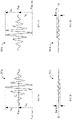
- FIGS. 3A - 3C show illustrative plots 300 of the signals seen by a conventional switchable capacitor 205 of FIG. 2 .
- FIG. 3A shows an illustrative power amplifier 110 output signal, such as could be seen at node A.
- the signal in FIG. 3A can be a portion of an amplitude-modulated radiofrequency signal.
- the signal can have a voltage swing around V DD , and the peak voltage swing (V P ) can be characterized as an absolute magnitude voltage difference between V DD and a maximum or minimum voltage output of the signal.
- FIG. 3B shows a plot 300b of an illustrative signal that can be seen at internal node B of the switchable capacitor 205 in response to the power amplifier 110 output signal of FIG. 3A , when the switchable capacitor 205 is ON.
- the switchable capacitor 205 is ON (i.e., current is flowing through the transistor 214)
- FIG. 3C shows a plot 300c of an illustrative signal that can be seen at internal node B of the switchable capacitor 205 in response to the power amplifier 110 output signal of FIG. 3A , when the switchable capacitor 205 is OFF.
- the switchable capacitor 205 is OFF (i.e., current is not flowing through the transistor 214)
- the internal node B is biased at V DD using the large bias resistor 212.
- the maximum voltage seen by the transistor 214 (the maximum drain-to-gate voltage (V DG ) and the maximum drain to source voltage (V DS )) is V P + V DD .
- V DG maximum drain-to-gate voltage
- V DS maximum drain to source voltage
- Some conventional approaches simply avoid such concerns by selecting a single capacitor, such that the resonant circuit is not tunable.
- Other conventional approaches provide a node (e.g., a pin) by which an off-chip capacitor of a selected value can be coupled with an on-chip inductor to tune the circuit for a particular application.
- Other conventional approaches can provide multiple capacitor options, which can be physically coupled with, or decoupled from, the inductor using by hard-wiring (e.g., forming or severing a conductive pathway), by using a physical switch component (e.g., a dip switch), etc.
- hard-wiring e.g., forming or severing a conductive pathway
- a physical switch component e.g., a dip switch
- Embodiments described herein include novel approaches to tunable output networks for radiofrequency power amplifiers in a manner that permits transistorswitching of capacitor options, while reducing stress on the transistor switches.
- embodiments include differential switchable capacitors.
- Some implementations include double-ended differential switchable capacitors, and other implementations include single-ended differential switchable capacitors.
- FIG. 4 shows a circuit diagram of an illustrative double-ended differential switchable capacitor 400, according to various embodiments.
- the differential switchable capacitor 400 includes a positive differential terminal 450, a negative differential terminal 460, a capacitor control switch (CCS) 410, a first capacitor 455, a second capacitor 465, and a switch network 470.
- the CCS 410 has a positive CCS node 412 and a negative CCS node 414.
- the CCS 410 operates to selectively toggle between a first mode and a second mode (e.g., ON and OFF modes) in response to a CCS control signal 415.
- a first mode and a second mode e.g., ON and OFF modes
- the CCS 410 is a MOS transistor (e.g., an NMOS), and the CCS control signal 415 is used to turn the CCS 410 (transistor) ON or OFF (i.e., such that the CCS 410 conducts or does not conduct, respectively).
- the first capacitor 455 is coupled between the positive CCS node 412 and the positive differential terminal 450
- the second capacitor 465 is coupled between the negative CCS node 414 and the negative differential terminal 460.
- turning the CCS 410 ON permits current to flow between the positive differential terminal 450 and the negative differential terminal 460 through the first capacitor 455 and the second capacitor 465. This can be considered as forming a capacitive channel through the differential switchable capacitor 400.
- the switch network 470 selectively toggles between the first mode and the second mode in response to a switch network control signal 425.
- the switch network 470 In the first mode, the switch network 470 is to pull the positive CCS node 412 and the negative CCS node 414 to a low reference voltage level (e.g., ground).
- the switch network 470 In the second mode, the switch network 470 is to pull the positive CCS node 412 and the negative CCS node 414 to a high reference voltage level (e.g., V DD 405).
- the switch network 470 includes two portions, and each portion includes a respective switch 420, positive bias resistor 424, and negative bias resistor 426.
- each positive bias resistor 424 and negative bias resistor 426 are relatively large resistors (e.g., 10 kilo-ohms, 100 kilo-ohms, etc.), such that the bias resistors have higher impedance than the first capacitor 455 and the second capacitor 465 at the operating radiofrequency frequency range.
- the positive bias resistor 424 and negative bias resistor 426 can have nominally identical resistance values.
- the positive bias resistors 424 and negative bias resistors 426 in both portions of the switch network 470 have nominally identical resistance values.
- each portion of the switch network 470 can also include a respective filter capacitor 422 to filter the drain of its respective switch 420. For example, the filtering can be helpful in case where there is an imbalance between the differential terminals 450 and 460 (e.g., where the positive bias resistor 424 and negative bias resistor 426 in a portion of the switch network 470 do not provide equal resistance).
- the differential switchable capacitor 400 is turned ON by turning ON the CCS 410, turning ON the switch 420b of the second portion of the switch network 470b, and turning OFF the switch 420a of the first portion of the switch network 470a.
- the CCS 415 is an NMOS transistor
- switch 420a is a PMOS transistor
- switch 420b is an NMOS transistor.
- the differential switchable capacitor 400 is turned ON by applying V DD 405 to the gates of all of CCS 410, switch 420b, and switch 420a.
- the CCS 410 effectively directly connects the first capacitor 455 with the second capacitor 465, thereby forming a capacitive channel between the positive differential terminal 450 and the negative differential terminal 460.
- Concurrently turning the second portion of the switch network 470b ON (and turning the first portion of the switch network 470a OFF) can effectively cause the first capacitor 455 to be coupled between the positive differential terminal 450 and ground (via bias resistor 424b), and can cause the second capacitor 465 to be coupled between the negative differential terminal 460 and ground (via bias resistor 426b).
- the positive CCS node 412 and the negative CCS node 414 are biased to ground.
- the differential switchable capacitor 400 is turned OFF by turning OFF the CCS 410, turning ON switch 420a, and turning OFF switch 420b.
- the differential switchable capacitor 400 is turned OFF by applying a low voltage V B to the gate of CCS 410, and applying a zero voltage to the gates of switch 420a and switch 420b.
- Turning OFF the CCS 410 effectively decouples the first capacitor 455 from the second capacitor 465
- Concurrently turning the first portion of the switch network 470a ON (and turning the second portion of the switch network 470b OFF) can effectively cause the first capacitor 455 to be coupled between the positive differential terminal 450 and V DD 405 (via bias resistor 424a), and can cause the second capacitor 465 to be coupled between the negative differential terminal 460 and V DD 405 (via bias resistor 426a).
- V DD - V P defines a minimum voltage level (V OUT_MIN ) of the voltage signal seen at the positive CCS node 412 and the negative CCS node 414.
- V OUT_MIN a minimum voltage level of the voltage signal seen at the positive CCS node 412 and the negative CCS node 414.
- V P is less than V DD
- FIGS. 5A - 5D show illustrative plots 500 of the signals seen by embodiments of novel differential switchable capacitors described herein, such as the differential switchable capacitor 400 of FIG. 4 .
- FIGS. 5A and 5B show an illustrative power amplifier 110 output signal as received differentially by the differential terminals of the differential switchable capacitor (e.g., the positive differential terminal 450 and the negative differential terminal 460).
- the signal shown in the plot 500b of FIG. 5B is complementary to (e.g., an inversion of) the signal shown in the plot 500a of FIG. 5A .
- One of the differential terminals receives a signal that corresponds directly to the power amplifier 110 output signal, and the other of the differential terminals receives a signal that corresponds to a complement of the power amplifier 110 output signal.
- the power amplifier 110 outputs differential signals, and each differential output signal is received by a corresponding one of the differential terminals.
- one differential terminal is coupled directly with the output of the power amplifier 110, and the other differential terminal is coupled with the output of the power amplifier 110 via an inverter (e.g., an inverting operational amplifier, or the like) that generates the complementary signal.
- the signals have a voltage swing around V DD , and the peak voltage swing (V P ) is characterized as an absolute magnitude voltage difference between V DD and a maximum or minimum voltage output of the signal.
- the CCS of the differential switchable capacitor is OFF, and the internal nodes (positive CCS node 412 and negative CCS node 414) are biased to V DD 405.
- the voltage signal seen at the internal nodes substantially matches the voltage signals seen at the differential terminals.
- the voltage signal seen at the positive CCS node tracks the voltage signal seen at the positive differential terminal
- the voltage signal seen at the negative CCS node tracks the voltage signal seen at the negative differential terminal.
- FIGS. 5A and 5B can also describe the voltage signal seen at the internal nodes when the differential switchable capacitor is OFF.
- FIGS. 5C and 5D show plots 500c and 500d of illustrative signals that can be seen at internal nodes of the differential switchable capacitor in response to the differential power amplifier 110 output signals of FIGS. 5A and 5B , when the differential switchable capacitor is ON.
- the CCS of the differential switchable capacitor is ON, and the internal nodes (positive CCS node and negative CCS node) are biased to ground.
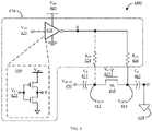
- FIG. 6 shows a circuit diagram of another illustrative differential switchable capacitor 600, according to various embodiments.
- the differential switchable capacitor 600 can operate in a substantially similar manner to that of the differential switchable capacitor 400 of FIG. 4 .
- the differential switchable capacitor 600 includes a positive differential terminal 450, a negative differential terminal 460, a capacitor control switch (CCS) 410, a first capacitor 455, a second capacitor 465, and a switch network 670.
- the CCS 410 has a positive CCS node 412 and a negative CCS node 414.
- the CCS 410 operates to selectively toggle between a first mode and a second mode (e.g., ON and OFF modes) in response to a CCS control signal 415.
- a first mode and a second mode e.g., ON and OFF modes
- the CCS 410 is a MOS transistor (e.g., an NMOS), and the CCS control signal 415 can be used to turn the CCS 410 (transistor) ON or OFF (i.e., such that the CCS 410 conducts or does not conduct, respectively).
- the first capacitor 455 is coupled between the positive CCS node 412 and the positive differential terminal 450
- the second capacitor 465 is coupled between the negative CCS node 414 and the negative differential terminal 460.
- turning the CCS 410 ON permits current to flow between the positive differential terminal 450 and the negative differential terminal 460 through the first capacitor 455 and the second capacitor 465. This can be considered as forming a capacitive channel through the differential switchable capacitor 600.
- the switch network 670 selectively toggles between the first mode and the second mode in response to a switch network control signal 425.
- the switch network 670 In the first mode, the switch network 670 is to pull the positive CCS node 412 and the negative CCS node 414 to a low reference voltage level (e.g., ground).
- the switch network 670 In the second mode, the switch network 670 is to pull the positive CCS node 412 and the negative CCS node 414 to a high reference voltage level (e.g., V DD 405).
- the switch network 670 includes an inverter 610.
- the inverter can include two switched implemented as complementary MOS (CMOS) transistors.
- CMOS complementary MOS
- a PMOS transistor is coupled between V DD 405 and an output node "X"
- an NMOS transistor is coupled between the X node and ground.
- the CCS control signal 415 is coupled to the gates of both CMOS transistors. As such, asserting the CCS control signal 415 (e.g., biasing the CCS control signal 415 to V DD 405) turns OFF the PMOS transistor and turns ON the NMOS transistor, thereby pulling the X node to ground; and de-asserting the CCS control signal 415 (e.g., biasing the CCS control signal 415 to ground) turns ON the PMOS transistor and turns OFF the NMOS transistor, thereby pulling the X node to V DD 405.
- asserting the CCS control signal 415 e.g., biasing the CCS control signal 415 to V DD 405
- asserting the CCS control signal 415 turns OFF the PMOS transistor and turns ON the NMOS transistor, thereby pulling the X node to ground
- the positive CCS node 412 is coupled to the X node (the output of the inverter 610) via a positive bias resistor 424
- the negative CCS node 414 is coupled to the X node via a negative bias resistor 426.
- asserting the CCS control signal 415 effectively pulls the positive CCS node 412 and the negative CCS node 414 to ground (via the positive bias resistor 424 and the negative bias resistor 426); and de-asserting the CCS control signal 415 effectively pulls the positive CCS node 412 and the negative CCS node 414 to V DD 405 (via the same positive bias resistor 424 and the same negative bias resistor 426).
- the differential switchable capacitor 600 can operate in ON and OFF modes.
- the ON mode the differential switchable capacitor 600 is turned ON by turning ON the CCS 410 and asserting the CCS control signal 415 (i.e., biasing the internal nodes to ground).
- the OFF mode the differential switchable capacitor 600 is turned OFF by turning OFF the CCS 410 and de-asserting the CCS control signal 415 (i.e., biasing the internal nodes to V DD 405).
- FIGS. 4 and 6 show two possible implementations of differential switchable capacitors, as described herein.
- the switched capacitor network 135 can include multiple of the differential switchable capacitors arranged in parallel.
- the switched capacitor network 135 can include master differential inputs, shown as a master positive node 140 (corresponding to node A), and a master negative node 142 (corresponding to a complement of node A, or A ).
- the positive differential terminal 450 of each of the differential switchable capacitors is coupled with the master positive node 140
- the negative differential terminal 160 of each of the differential switchable capacitors is coupled with the master negative node 142.
- a master CCS control signal 137 can be used to direct the CCS control signal 415 of each differential switchable capacitor, thereby directing each differential switchable capacitor to be in its ON or OFF mode.
- the master CCS control signal 137 can be implemented as a single signal or multiple signals, and each signal can be implemented in any suitable manner.
- there are N differential switchable capacitors e.g., N being an integer greater than one
- the master CCS control signal 137 is an N-bit signal.
- each bit can be associated with a respective one of the differential switchable capacitors, such that each differential switchable capacitor can be selectively toggled between the first (e.g., ON) mode and the second (e.g., OFF) mode responsive to the associated bit of the CCS control signal.
- a master CCS control signal 137 of '01000' can be used to turn on the second of the five differential switchable capacitors; or a master CCS control signal 137 of '01100' can be used to turn on the second and third of the five differential switchable capacitors (in implementations that permit concurrent activation of multiple of the differential switchable capacitors).
- the differential switchable capacitor 600 can be implemented in a single-ended configuration by tying its negative differential terminal 460 to ground (illustrated in FIG. 6 as the dashed path to ground node 620).
- the so-called differential switchable capacitors of a switched capacitor network 135 can operate in a non-differential manner.
- all the switchable capacitors of a switched capacitor network 135 can have their respective negative differential terminals 460 tied to ground, and their respective positive differential terminals 450 tied to the master positive node 140 (e.g., without using the master negative node 142).
- FIG. 7 shows a flow diagram of an illustrative method 700 for tuning a resonant circuit using differential switchable capacitors, according to various embodiments.
- Embodiments of the method 700 can begin at stage 704 by applying a capacitor control switch (CCS) control signal to a switchable capacitor system having multiple differential switchable capacitors.
- the CCS control signal can identify a particular (one or more) differential switchable capacitor of the differential switchable capacitors, such that applying the CCS control signal causes the identified differential switchable capacitor to turn ON. Turning the differential switchable capacitor ON can thereby couple a positive differential terminal with a negative differential terminal via a capacitive channel of the identified differential switchable capacitor.
- CCS capacitor control switch
- the capacitive channel can be one of multiple capacitive channels, each comprised by a respective one of the differential switchable capacitors.
- Each capacitive channel can have an associated (e.g., different) capacitance defined by a respective first capacitor and a respective second capacitor and can have a respective CCS responsive to the CCS control signal.
- Each respective first capacitor can be coupled between the respective CCS and the positive differential terminal, and each respective second capacitor can be coupled between the respective CCS and the negative differential terminal.
- applying the CCS control signal at stage 704 includes applying a high reference voltage to the respective CCS of the capacitive channel comprised by the identified differential switchable capacitor to turn ON the identified differential switchable capacitor.
- the applying at stage 704 includes applying a low control voltage to the respective CCS of at least another capacitive channel comprised by at least another of the differential switchable capacitors to turn OFF the at least another of the differential switchable capacitors.
- the low control voltage is greater than zero and set to a level in accordance with the high reference voltage minus a peak signal voltage of the first data signal.
- embodiments apply a first data signal to the positive differential terminal.
- the first data signal corresponds to an output signal from a power amplifier in electrical communication with the positive differential terminal.
- embodiments apply a second data signal to the negative differential terminal.
- the second data signal is a complement of the first data signal.
- a first element, component, discussed below could be termed a second element, component, without departing from the teachings of the present application.
- the terms “logic low,” “low state,” “low level,” “logic low level,” “low,” or “0” are used interchangeably.
- logic high “high state,” “high level,” “logic high level,” “high,” or “1” are used interchangeably.
- the terms “a”, “an” and “the” may include singular and plural references. It will be further understood that the terms “comprising”, “including”, having” and variants thereof, when used in this specification, specify the presence of stated features, steps, operations, elements, and/or components, but do not preclude the presence or addition of one or more other features, steps, operations, elements, components, and/or groups thereof. In contrast, the term “consisting of' when used in this specification, specifies the stated features, steps, operations, elements, and/or components, and precludes additional features, steps, operations, elements and/or components. Furthermore, as used herein, the words “and/or” may refer to and encompass any possible combinations of one or more of the associated listed items.
Landscapes
- Engineering & Computer Science (AREA)
- Power Engineering (AREA)
- Amplifiers (AREA)
Claims (13)
- Schaltbares Kondensatorsystem, umfassend:
einen differenziellen schaltbaren Kondensator (400, 600), umfassend:einen positiven differenziellen Anschluss (450), der eingerichtet ist, ein positives differenzielles Ausgangssignal zu empfangen, das in einem Ausgangssignal von einem Hochfrequenz-Leistungsverstärker (110) enthalten ist;einen negativen differenziellen Anschluss (460), der eingerichtet ist, ein negatives differenzielles Ausgangssignal zu empfangen, das in dem Ausgangssignal von dem Hochfrequenz-Leistungsverstärker (110) enthalten ist;wobei sowohl das positive als auch das negative differenzielle Ausgangssignal eine Spannungsschwankung ungleich Null um eine hohe Referenzspannung (VDD) und eine Spitzenspannungsschwankung aufweisen, die als eine absolute Spannungsdifferenzhöhe zwischen der hohen Referenzspannung (VDD) und einer maximalen oder minimalen Spannung der Spannungsschwankung ungleich Null definiert ist;einen Kondensatorsteuerschalter, CCS (410), der mittels eines MOS-Transistors mit einem positiven CCS-Knoten (412) und einem negativen CCS-Knoten (414) implementiert ist, wobei der CCS (410) eingerichtet ist, als Reaktion auf ein CCS-Steuersignal (415), das an einen Gate-Knoten des MOS-Transistors angelegt ist, selektiv zwischen einem ersten Modus und einem zweiten Modus umzuschalten;einen ersten Kondensator (455), der zwischen den positiven CCS-Knoten (412) und den positiven differenziellen Anschluss (450) gekoppelt ist;
einen zweiten Kondensator (465), der zwischen den negativen CCS-Knoten (414) und den negativen differenziellen Anschluss (460) gekoppelt ist; undein Schaltnetzwerk (470), das eingerichtet ist, in Reaktion auf ein Schaltnetzwerksteuersignal (425) selektiv zwischen dem ersten Modus und dem zweiten Modus umzuschalten, so dass:im ersten Modus das CCS-Steuersignal (415) auf die hohe Referenzspannung eingestellt ist, um den ersten Kondensator (455) direkt mit dem zweiten Kondensator (465) zu verbinden, und das Schaltnetzwerk (470) eingerichtet ist, den positiven CCS-Knoten (412) und den negativen CCS-Knoten (414) auf einen niedrigen Referenzspannungspegel zu ziehen; undim zweiten Modus das CCS-Steuersignal (415) auf eine niedrige Steuerspannung eingestellt ist, um den ersten Kondensator (455) von dem zweiten Kondensator (465) zu trennen, und das Schaltnetzwerk (470) eingerichtet ist, den positiven CCS-Knoten (412) und den negativen CCS-Knoten (414) auf den hohen Referenzspannungspegel zu ziehen, wobei die niedrige Steuerspannung größer ist als Null und auf einen Pegel eingestellt ist, der gleich der hohen Referenzspannung minus der Spitzenspannungsschwankung ist;wobei das Schaltnetzwerk (470) umfasst:ein erstes Unternetzwerk (470a), aufweisend einen ersten Schalter (420a); undein zweites Unternetzwerk (470b), aufweisend einen zweiten Schalter (420b),so dass im ersten Modus das erste Unternetzwerk (470a) eingerichtet ist, den positiven CCS-Knoten (412) und den negativen CCS-Knoten (414) von dem hohen Referenzspannungspegel zu entkoppeln, und das zweite Unternetzwerk (470b) eingerichtet ist, den positiven CCS-Knoten (412) und den negativen CCS-Knoten (414) mit dem niedrigen Referenzspannungspegel zu koppeln, undso dass im zweiten Modus das erste Unternetzwerk (470a) eingerichtet ist, den positiven CCS-Knoten (412) und den negativen CCS-Knoten (414) mit dem hohen Referenzspannungspegel zu koppeln, und das zweite Unternetzwerk (470b) eingerichtet ist, den positiven CCS-Knoten (412) und den negativen CCS-Knoten (414) von dem niedrigen Referenzspannungspegel zu entkoppeln;wobei das erste Unternetzwerk (470a) einen ersten Widerstand (424a), der zwischen den ersten Schalter (420a) und den positiven CCS-Knoten (412) gekoppelt ist, und einen zweiten Widerstand (426a), der zwischen den ersten Schalter (420a) und den negativen CCS-Knoten (414) gekoppelt ist, aufweist; unddas zweite Unternetzwerk (470b) einen dritten Widerstand (424b), der zwischen den zweiten Schalter (420b) und den positiven CCS-Knoten (412) gekoppelt ist, und einen vierten Widerstand (426b), der zwischen den zweiten Schalter (420b) und den negativen CCS-Knoten (414) gekoppelt ist, aufweist. - Schaltbares Kondensatorsystem nach Anspruch 1, wobei:im ersten Modus der differenzielle schaltbare Kondensator (400) durch Einschalten des CCS (410), Einschalten des zweiten Schalters (420b) und Ausschalten des ersten Schalters (420a) eingeschaltet wird; undim zweiten Modus der differenzielle schaltbare Kondensator (400) durch Ausschalten des CCS (410), Einschalten des ersten Schalters (420a) und Ausschalten des zweiten Schalters (420b) ausgeschaltet wird.
- Schaltbares Kondensatorsystem nach Anspruch 2, wobei:das erste Unternetzwerk (470a) ferner einen ersten Filterkondensator (422a) parallel zum ersten Schalter (420a) aufweist; unddas zweite Unternetzwerk (470b) ferner einen zweiten Filterkondensator (422b) parallel zum zweiten Schalter (420b) aufweist.
- Schaltbares Kondensatorsystem, umfassend:
einen differenziellen schaltbaren Kondensator (400, 600), umfassend:einen positiven differenziellen Anschluss (450), der eingerichtet ist, ein Ausgangssignal von einem Hochfrequenz-Leistungsverstärker (110) zu empfangen;einen negativen differenziellen Anschluss (460);wobei das Ausgangssignal eine Spannungsschwankung ungleich Null um eine hohe Referenzspannung (VDD) und eine Spitzenspannungsschwankung aufweist, die als eine absolute Spannungsdifferenzhöhe zwischen der hohen Referenzspannung (VDD) und einer maximalen oder minimalen Spannung der Spannungsschwankung ungleich Null definiert ist;einen Kondensatorsteuerschalter, CCS (410), der mittels eines MOS-Transistors mit einem positiven CCS-Knoten (412) und einem negativen CCS-Knoten (414) implementiert ist, wobei der CCS (410) eingerichtet ist, als Reaktion auf ein CCS-Steuersignal (415), das an einen Gate-Knoten des MOS-Transistors angelegt ist, selektiv zwischen einem ersten Modus und einem zweiten Modus umzuschalten;einen ersten Kondensator (455), der zwischen den positiven CCS-Knoten (412) und den positiven differenziellen Anschluss (450) gekoppelt ist;einen zweiten Kondensator (465), der zwischen den negativen CCS-Knoten (414) und den negativen differenziellen Anschluss (460) gekoppelt ist; undein Schaltnetzwerk (670), das eingerichtet ist, in Reaktion auf ein Schaltnetzwerksteuersignal (425) selektiv zwischen dem ersten Modus und dem zweiten Modus umzuschalten, so dass:im ersten Modus das CCS-Steuersignal (415) auf die hohe Referenzspannung eingestellt ist, um den ersten Kondensator (455) direkt mit dem zweiten Kondensator (465) zu verbinden, und das Schaltnetzwerk (670) eingerichtet ist, den positiven CCS-Knoten (412) und den negativen CCS-Knoten (414) auf einen niedrigen Referenzspannungspegel zu ziehen; undim zweiten Modus das CCS-Steuersignal (415) auf eine niedrige Steuerspannung eingestellt ist, um den ersten Kondensator (455) von dem zweiten Kondensator (465) zu trennen, und das Schaltnetzwerk (670) eingerichtet ist, den positiven CCS-Knoten (412) und den negativen CCS-Knoten (414) auf den hohen Referenzspannungspegel zu ziehen, wobei die niedrige Steuerspannung größer ist als Null und auf einen Pegel eingestellt ist, der gleich der hohen Referenzspannung minus der Spitzenspannungsschwankung ist;wobei das Schaltnetzwerk (670) umfasst:einen Wechselrichter (610), der eingerichtet ist, in Reaktion auf das Schaltnetzwerksteuersignal (425) einen Wechselrichterausgang an einem Wechselrichterausgangsknoten zu erzeugen;einen ersten Widerstand (424), der zwischen den Wechselrichterausgangsknoten und den positiven CCS-Knoten (412) gekoppelt ist; undeinen zweiten Widerstand (426), der zwischen den Wechselrichterausgangsknoten und den negativen CCS-Knoten (414) gekoppelt ist;wobei der negative differenzielle Anschluss (460) mit einer Erdungsreferenz (620) gekoppelt ist. - Schaltbares Kondensatorsystem nach Anspruch 4, wobei:im ersten Modus der CCS (410) eingeschaltet ist, wodurch der erste Kondensator (455) direkt mit dem zweiten Kondensator (465) verbunden wird; undim zweiten Modus der CCS ausgeschaltet ist, wodurch der erste Kondensator (455) vom zweiten Kondensator (465) getrennt wird.
- Schaltbares Kondensatorsystem nach einem der Ansprüche 1-5, ferner umfassend:einen positiven Master-Knoten (140); undeinen negativen Master-Knoten (142),wobei der differenzielle schaltbare Kondensator (400, 600) einer einer Vielzahl von differenziellen schaltbaren Kondensatoren ist,der positive differenzielle Anschluss (450) jedes der Vielzahl von differenziellen schaltbaren Kondensatoren mit dem positiven Master-Knoten (140) gekoppelt ist, undder negative differenzielle Anschluss (460) jedes der Vielzahl von differenziellen schaltbaren Kondensatoren mit dem negativen Master-Knoten (142) gekoppelt ist.
- Schaltbares Kondensatorsystem nach Anspruch 6, ferner umfassend:einen Master-Steuerknoten, um das CCS-Steuersignal (415) zu empfangen,wobei die Vielzahl von differenziellen schaltbaren Kondensatoren N differenzielle schaltbare Kondensatoren umfasst, wobei N eine ganze Zahl größer Eins ist, unddas CCS-Steuersignal (415) ein N-Bit-Signal ist, wobei jedes Bit einem jeweiligen der differenziell schaltbaren Kondensatoren zugeordnet ist, so dass jeder differenzielle schaltbare Kondensator (400, 600) in Reaktion auf das zugeordnete Bit des CCS-Steuersignals (415) selektiv zwischen dem ersten Modus und dem zweiten Modus umgeschaltet wird.
- Transceiver-System, umfassend:einen Leistungsverstärker (110) zum Erzeugen eines Ausgangssignals an einem Ausgangsanschluss als eine Funktion des Anlegens einer Verstärkung an ein Eingangssignal (102); undeinen Resonanzkreis (130), umfassend eine Induktivität (115) und ein schaltbares Kondensatorsystem nach einem der Ansprüche 1 bis 7, wobei das schaltbare Kondensatorsystem eine Vielzahl von differenziellen schaltbaren Kondensatoren umfasst und ein positiver differenzieller Anschluss in jedem schaltbaren differenziellen Kondensator mit dem Ausgangsanschluss gekoppelt ist, um ein erstes differenzielles Eingangssignal als Reaktion auf das Ausgangssignal zu empfangen.
- Schaltbares Kondensatorsystem nach Anspruch 8, wobei:
ein negativer differenzieller Anschluss mit dem Ausgangsanschluss gekoppelt ist, um ein zweites differenzielles Eingangssignal zu empfangen, das einem Komplement des ersten differenziellen Eingangssignals entspricht. - Verfahren (700) zum Abstimmen eines Resonanzkreises unter Verwendung eines differenziellen schaltbaren Kondensators in einem schaltbaren System, wobei das Verfahren umfasst:Empfangen, an einem positiven differenziellen Anschluss (450), des differenziellen schaltbaren Kondensators (400, 600), eines positiven differenziellen Ausgangssignals, das in einem Ausgangssignal von einem Hochfrequenz-Leistungsverstärker (110) enthalten ist;Empfangen, an einem negativen differenziellen Anschluss (460) des differenziellen schaltbaren Kondensators (400, 600), eines negativen differenziellen Ausgangssignals, das in dem Ausgangssignal von dem Hochfrequenz-Leistungsverstärker (110) enthalten ist;wobei sowohl das positive als auch das negative differenzielle Ausgangssignal eine Spannungsschwankung ungleich Null um eine hohe Referenzspannung (VDD) und eine Spitzenspannungsschwankung aufweisen, die als eine absolute Spannungsdifferenzhöhe zwischen der hohen Referenzspannung (VDD) und einer maximalen oder minimalen Spannung der Spannungsschwankung ungleich Null definiert ist;selektives Umschalten eines Kondensatorsteuerschalters, CCS (410), der mittels eines MOS-Transistors mit einem positiven CCS-Knoten (412) und einem negativen CCS-Knoten (414) implementiert ist, als Reaktion auf ein CCS-Steuersignal (415), das an einen Gate-Knoten des MOS-Transistors angelegt ist, zwischen einem ersten Modus und einem zweiten Modus;wobei ein erster Kondensator (455) zwischen den positiven CCS-Knoten (412) und den positiven differenziellen Anschluss (450) gekoppelt ist;ein zweiter Kondensator (465) zwischen den negativen CCS-Knoten (414) und den negativen differenziellen Anschluss (460) gekoppelt ist; undselektives Umschalten eines Schaltnetzwerks (470) in Reaktion auf ein Schaltnetzwerksteuersignal (425) zwischen dem ersten Modus und dem zweiten Modus durch:im ersten Modus, Einstellen des CCS-Steuersignals (415) auf die hohe Referenzspannung, um den ersten Kondensator (455) direkt mit dem zweiten Kondensator (465) zu verbinden, und Ziehen, mittels des Schaltnetzwerks (470), des positiven CCS-Knotens (412) und des negativen CCS-Knotens (414) auf einen niedrigen Referenzspannungspegel; undim zweiten Modus, Einstellen des CCS-Steuersignals (415) auf eine niedrige Steuerspannung, um den ersten Kondensator (455) von dem zweiten Kondensator (465) zu trennen, und Ziehen, mittels des Schaltnetzwerks (470), des positiven CCS-Knotens (412) und des negativen CCS-Knotens (414) auf den hohen Referenzspannungspegel, wobei die niedrige Steuerspannung größer ist als Null und auf einen Pegel eingestellt ist, der gleich der hohen Referenzspannung minus der Spitzenspannungsschwankung ist;wobei das Schaltnetzwerk (470) umfasst:ein erstes Unternetzwerk (470a), aufweisend einen ersten Schalter (420a); undein zweites Unternetzwerk (470b), aufweisend einen zweiten Schalter (420b),so dass das erste Unternetzwerk (470a) im ersten Modus den positiven CCS-Knoten (412) und den negativen CCS-Knoten (414) von dem hohen Referenzspannungspegel entkoppelt, und das zweite Unternetzwerk (470b) den positiven CCS-Knoten (412) und den negativen CCS-Knoten (414) mit dem niedrigen Referenzspannungspegel koppelt, undso dass das erste Unternetzwerk (470a) im zweiten Modus den positiven CCS-Knoten (412) und den negativen CCS-Knoten (414) mit dem hohen Referenzspannungspegel koppelt, und das zweite Unternetzwerk (470b) den positiven CCS-Knoten (412) und den negativen CCS-Knoten (414) von dem niedrigen Referenzspannungspegel entkoppelt;wobei das erste Unternetzwerk (470a) einen ersten Widerstand (424a), der zwischen den ersten Schalter (420a) und den positiven CCS-Knoten (412) gekoppelt ist, und einen zweiten Widerstand (426a), der zwischen den ersten Schalter (420a) und den negativen CCS-Knoten (414) gekoppelt ist, aufweist; unddas zweite Unternetzwerk (470b) einen dritten Widerstand (424b), der zwischen den zweiten Schalter (420b) und den positiven CCS-Knoten (412) gekoppelt ist, und einen vierten Widerstand (426b), der zwischen den zweiten Schalter (420b) und den negativen CCS-Knoten (414) gekoppelt ist, aufweist.
- Verfahren (700) nach Anspruch 10, wobei:im ersten Modus der differenzielle schaltbare Kondensator (400) durch Einschalten des CCS (410), Einschalten des zweiten Schalters (420b) und Ausschalten des ersten Schalters (420a) eingeschaltet wird; undim zweiten Modus der differenzielle schaltbare Kondensator (400) durch Ausschalten des CCS (410), Einschalten des ersten Schalters (420a) und Ausschalten des zweiten Schalters (420b) ausgeschaltet wird.
- Verfahren (700) zum Abstimmen eines Resonanzkreises unter Verwendung eines differenziellen schaltbaren Kondensators in einem schaltbaren System, wobei das Verfahren umfasst:Empfangen, an einem positiven differenziellen Anschluss (450) des differenziellen schaltbaren Kondensators (400, 600), eines Ausgangssignals von einem Hochfrequenz-Leistungsverstärker (110);wobei das Ausgangssignal eine Spannungsschwankung ungleich Null um eine hohe Referenzspannung (VDD) und eine Spitzenspannungsschwankung aufweist, die als eine absolute Spannungsdifferenzhöhe zwischen der hohen Referenzspannung (VDD) und einer maximalen oder minimalen Spannung der Spannungsschwankung ungleich Null definiert ist;selektives Umschalten eines Kondensatorsteuerschalters, CCS (410), der mittels eines MOS-Transistors mit einem positiven CCS-Knoten (412) und einem negativen CCS-Knoten (414) implementiert ist, als Reaktion auf ein CCS-Steuersignal (415), das an einen Gate-Knoten des MOS-Transistors angelegt ist, zwischen einem ersten Modus und einem zweiten Modus;wobei ein erster Kondensator (455) zwischen den positiven CCS-Knoten (412) und den positiven differenziellen Anschluss (450) gekoppelt ist;ein zweiter Kondensator (465) zwischen den negativen CCS-Knoten (414) und den negativen differenziellen Anschluss (460) gekoppelt ist; undselektives Umschalten eines Schaltnetzwerks (670) in Reaktion auf ein Schaltnetzwerksteuersignal (425) zwischen dem ersten Modus und dem zweiten Modus durch:im ersten Modus, Einstellen des CCS-Steuersignals (415) auf die hohe Referenzspannung, um den ersten Kondensator (455) direkt mit dem zweiten Kondensator (465) zu verbinden, und Ziehen, mittels des Schaltnetzwerks (670), des positiven CCS-Knotens (412) und des negativen CCS-Knotens (414) auf einen niedrigen Referenzspannungspegel; undim zweiten Modus, Einstellen des CCS-Steuersignals (415) auf eine niedrige Steuerspannung, um den ersten Kondensator (455) von dem zweiten Kondensator (465) zu trennen, und Ziehen, mittels des Schaltnetzwerks (670), des positiven CCS-Knotens (412) und des negativen CCS-Knotens (414) auf den hohen Referenzspannungspegel, wobei die niedrige Steuerspannung größer ist als Null und auf einen Pegel eingestellt ist, der gleich der hohen Referenzspannung minus der Spitzenspannungsschwankung ist;wobei das Schaltnetzwerk (670) umfasst:einen Wechselrichter (610), um in Reaktion auf das Schaltnetzwerksteuersignal (425) einen Wechselrichterausgang an einem Wechselrichterausgangsknoten zu erzeugen;einen ersten Widerstand (424), der zwischen den Wechselrichterausgangsknoten und den positiven CCS-Knoten (412) gekoppelt ist; undeinen zweiten Widerstand (426), der zwischen den Wechselrichterausgangsknoten und den negativen CCS-Knoten (414) gekoppelt ist;wobei der negative differenzielle Anschluss (460) mit einer Erdungsreferenz (620) gekoppelt ist.
- Verfahren (700) nach Anspruch 12, wobei:im ersten Modus der CCS (410) eingeschaltet wird, wodurch der erste Kondensator CCS (455) direkt mit dem zweiten Kondensator (465) verbunden wird; undim zweiten Modus der CCS ausgeschaltet wird, wodurch der erste Kondensator (455) vom zweiten Kondensator (465) getrennt wird.
Applications Claiming Priority (2)
| Application Number | Priority Date | Filing Date | Title |
|---|---|---|---|
| US16/395,222 US10862425B2 (en) | 2019-04-25 | 2019-04-25 | Differential switchable capacitors for radiofrequency power amplifiers |
| PCT/CN2019/111145 WO2020215621A1 (en) | 2019-04-25 | 2019-10-15 | Differential switchable capacitors for radiofrequency power amplifiers |
Publications (3)
| Publication Number | Publication Date |
|---|---|
| EP3759818A1 EP3759818A1 (de) | 2021-01-06 |
| EP3759818A4 EP3759818A4 (de) | 2021-06-30 |
| EP3759818B1 true EP3759818B1 (de) | 2022-12-28 |
Family
ID=72917352
Family Applications (1)
| Application Number | Title | Priority Date | Filing Date |
|---|---|---|---|
| EP19920624.4A Active EP3759818B1 (de) | 2019-04-25 | 2019-10-15 | Schaltbare differenzialkondensatoren für hochfrequenzleistungsverstärker |
Country Status (4)
| Country | Link |
|---|---|
| US (1) | US10862425B2 (de) |
| EP (1) | EP3759818B1 (de) |
| CN (1) | CN111149292B (de) |
| WO (1) | WO2020215621A1 (de) |
Family Cites Families (11)
| Publication number | Priority date | Publication date | Assignee | Title |
|---|---|---|---|---|
| US6889036B2 (en) * | 2002-03-07 | 2005-05-03 | Freescale Semiconductor, Inc. | Integrated frequency selectable resonant coupling network and method thereof |
| US7038552B2 (en) * | 2003-10-07 | 2006-05-02 | Analog Devices, Inc. | Voltage controlled oscillator having improved phase noise |
| US7116183B2 (en) | 2004-02-05 | 2006-10-03 | Qualcomm Incorporated | Temperature compensated voltage controlled oscillator |
| US20070247237A1 (en) * | 2006-03-31 | 2007-10-25 | Broadcom Corporation | Technique for reducing capacitance of a switched capacitor array |
| US8044741B2 (en) * | 2008-01-17 | 2011-10-25 | Texas Instruments Incorporated | Systems and methods for reducing flicker noise in an oscillator |
| CN103001618B (zh) | 2012-11-02 | 2015-04-01 | 长沙景嘉微电子股份有限公司 | 一种寄生效应低品质因数高的差分开关电容结构 |
| US9411987B2 (en) | 2014-08-18 | 2016-08-09 | Qualcomm Incorporated | Low noise and low power passive sampling network for a switched-capacitor ADC with a slow reference generator |
| US9742353B2 (en) * | 2015-06-22 | 2017-08-22 | Avago Technologies General Ip (Singapore) Pte. Ltd. | CMOS VCO with implicit common-mode resonance |
| CN107404297A (zh) | 2016-05-19 | 2017-11-28 | 深圳市南方硅谷微电子有限公司 | 功率放大电路 |
| CN108631758A (zh) | 2017-03-17 | 2018-10-09 | 中芯国际集成电路制造(上海)有限公司 | 开关电容电路、射频器件和形成开关电容电路的方法 |
| EP3499718B1 (de) * | 2017-12-18 | 2021-07-07 | Stichting IMEC Nederland | Verbesserungen an oder in verbindung mit leistungsverstärkern mit geschaltetem kondensator |
-
2019
- 2019-04-25 US US16/395,222 patent/US10862425B2/en active Active
- 2019-10-15 CN CN201980002878.XA patent/CN111149292B/zh active Active
- 2019-10-15 WO PCT/CN2019/111145 patent/WO2020215621A1/en not_active Ceased
- 2019-10-15 EP EP19920624.4A patent/EP3759818B1/de active Active
Also Published As
| Publication number | Publication date |
|---|---|
| CN111149292B (zh) | 2023-12-08 |
| US20200343857A1 (en) | 2020-10-29 |
| CN111149292A (zh) | 2020-05-12 |
| EP3759818A1 (de) | 2021-01-06 |
| WO2020215621A1 (en) | 2020-10-29 |
| US10862425B2 (en) | 2020-12-08 |
| EP3759818A4 (de) | 2021-06-30 |
Similar Documents
| Publication | Publication Date | Title |
|---|---|---|
| US10804953B2 (en) | Method of using integrated transmitter and receiver front end module | |
| EP2599221B1 (de) | Hf-isolations-schaltkreis | |
| US8803616B2 (en) | Temperature compensation and coarse tune bank switches in a low phase noise VCO | |
| US11159146B2 (en) | Reconfigurable analog filter and integrated circuit including the same | |
| US8107917B2 (en) | High linearity tunable bandpass filter | |
| US20120286889A1 (en) | Systems and Methods for Wideband CMOS Voltage-Controlled Oscillators Using Reconfigurable Inductor Arrays | |
| CN1949662B (zh) | 用于超宽带应用的放大器装置和方法以及相关器件 | |
| US8838045B2 (en) | Sub-band duplexer with active frequency tuning | |
| JP7002468B2 (ja) | 増幅器 | |
| JP2001119251A (ja) | 二重通過帯域増幅回路及び無線周波受信ヘッド | |
| US9973173B2 (en) | Switch topology for switching filters multiplexers | |
| US10511344B1 (en) | Transceiver resonant receive switch | |
| US7885629B2 (en) | Circuit with Q-enhancement cell having programmable bias current slope | |
| US7061340B2 (en) | Differently-tuned VCO using inductively coupled varactors | |
| CN113541612A (zh) | 提供可编程电感器以使得能够实现宽调谐范围 | |
| US7091784B1 (en) | Tunable circuit including a switchable inductor | |
| US10862425B2 (en) | Differential switchable capacitors for radiofrequency power amplifiers | |
| CN113796018B (zh) | 多频带均衡器 | |
| US10826432B2 (en) | Quadrature oscillator | |
| US10312961B1 (en) | Transceiver resonant receive switch |
Legal Events
| Date | Code | Title | Description |
|---|---|---|---|
| STAA | Information on the status of an ep patent application or granted ep patent |
Free format text: STATUS: UNKNOWN |
|
| STAA | Information on the status of an ep patent application or granted ep patent |
Free format text: STATUS: THE INTERNATIONAL PUBLICATION HAS BEEN MADE |
|
| PUAI | Public reference made under article 153(3) epc to a published international application that has entered the european phase |
Free format text: ORIGINAL CODE: 0009012 |
|
| STAA | Information on the status of an ep patent application or granted ep patent |
Free format text: STATUS: REQUEST FOR EXAMINATION WAS MADE |
|
| 17P | Request for examination filed |
Effective date: 20200928 |
|
| AK | Designated contracting states |
Kind code of ref document: A1 Designated state(s): AL AT BE BG CH CY CZ DE DK EE ES FI FR GB GR HR HU IE IS IT LI LT LU LV MC MK MT NL NO PL PT RO RS SE SI SK SM TR |
|
| AX | Request for extension of the european patent |
Extension state: BA ME |
|
| REG | Reference to a national code |
Ref country code: DE Ref legal event code: R079 Ref document number: 602019023833 Country of ref document: DE Free format text: PREVIOUS MAIN CLASS: H03K0017060000 Ipc: H03F0001560000 |
|
| A4 | Supplementary search report drawn up and despatched |
Effective date: 20210528 |
|
| RIC1 | Information provided on ipc code assigned before grant |
Ipc: H03F 1/56 20060101AFI20210521BHEP Ipc: H03K 17/06 20060101ALI20210521BHEP Ipc: H03F 3/193 20060101ALI20210521BHEP Ipc: H03J 3/24 20060101ALI20210521BHEP Ipc: H03J 3/32 20060101ALI20210521BHEP |
|
| STAA | Information on the status of an ep patent application or granted ep patent |
Free format text: STATUS: EXAMINATION IS IN PROGRESS |
|
| 17Q | First examination report despatched |
Effective date: 20220203 |
|
| DAV | Request for validation of the european patent (deleted) | ||
| DAX | Request for extension of the european patent (deleted) | ||
| GRAP | Despatch of communication of intention to grant a patent |
Free format text: ORIGINAL CODE: EPIDOSNIGR1 |
|
| STAA | Information on the status of an ep patent application or granted ep patent |
Free format text: STATUS: GRANT OF PATENT IS INTENDED |
|
| INTG | Intention to grant announced |
Effective date: 20220919 |
|
| GRAS | Grant fee paid |
Free format text: ORIGINAL CODE: EPIDOSNIGR3 |
|
| GRAA | (expected) grant |
Free format text: ORIGINAL CODE: 0009210 |
|
| STAA | Information on the status of an ep patent application or granted ep patent |
Free format text: STATUS: THE PATENT HAS BEEN GRANTED |
|
| AK | Designated contracting states |
Kind code of ref document: B1 Designated state(s): AL AT BE BG CH CY CZ DE DK EE ES FI FR GB GR HR HU IE IS IT LI LT LU LV MC MK MT NL NO PL PT RO RS SE SI SK SM TR |
|
| REG | Reference to a national code |
Ref country code: GB Ref legal event code: FG4D |
|
| REG | Reference to a national code |
Ref country code: CH Ref legal event code: EP |
|
| REG | Reference to a national code |
Ref country code: AT Ref legal event code: REF Ref document number: 1541101 Country of ref document: AT Kind code of ref document: T Effective date: 20230115 |
|
| REG | Reference to a national code |
Ref country code: IE Ref legal event code: FG4D |
|
| REG | Reference to a national code |
Ref country code: DE Ref legal event code: R096 Ref document number: 602019023833 Country of ref document: DE |
|
| REG | Reference to a national code |
Ref country code: LT Ref legal event code: MG9D |
|
| PG25 | Lapsed in a contracting state [announced via postgrant information from national office to epo] |
Ref country code: SE Free format text: LAPSE BECAUSE OF FAILURE TO SUBMIT A TRANSLATION OF THE DESCRIPTION OR TO PAY THE FEE WITHIN THE PRESCRIBED TIME-LIMIT Effective date: 20221228 Ref country code: NO Free format text: LAPSE BECAUSE OF FAILURE TO SUBMIT A TRANSLATION OF THE DESCRIPTION OR TO PAY THE FEE WITHIN THE PRESCRIBED TIME-LIMIT Effective date: 20230328 Ref country code: LT Free format text: LAPSE BECAUSE OF FAILURE TO SUBMIT A TRANSLATION OF THE DESCRIPTION OR TO PAY THE FEE WITHIN THE PRESCRIBED TIME-LIMIT Effective date: 20221228 Ref country code: FI Free format text: LAPSE BECAUSE OF FAILURE TO SUBMIT A TRANSLATION OF THE DESCRIPTION OR TO PAY THE FEE WITHIN THE PRESCRIBED TIME-LIMIT Effective date: 20221228 |
|
| REG | Reference to a national code |
Ref country code: NL Ref legal event code: MP Effective date: 20221228 |
|
| REG | Reference to a national code |
Ref country code: AT Ref legal event code: MK05 Ref document number: 1541101 Country of ref document: AT Kind code of ref document: T Effective date: 20221228 |
|
| PG25 | Lapsed in a contracting state [announced via postgrant information from national office to epo] |
Ref country code: RS Free format text: LAPSE BECAUSE OF FAILURE TO SUBMIT A TRANSLATION OF THE DESCRIPTION OR TO PAY THE FEE WITHIN THE PRESCRIBED TIME-LIMIT Effective date: 20221228 Ref country code: LV Free format text: LAPSE BECAUSE OF FAILURE TO SUBMIT A TRANSLATION OF THE DESCRIPTION OR TO PAY THE FEE WITHIN THE PRESCRIBED TIME-LIMIT Effective date: 20221228 Ref country code: HR Free format text: LAPSE BECAUSE OF FAILURE TO SUBMIT A TRANSLATION OF THE DESCRIPTION OR TO PAY THE FEE WITHIN THE PRESCRIBED TIME-LIMIT Effective date: 20221228 Ref country code: GR Free format text: LAPSE BECAUSE OF FAILURE TO SUBMIT A TRANSLATION OF THE DESCRIPTION OR TO PAY THE FEE WITHIN THE PRESCRIBED TIME-LIMIT Effective date: 20230329 |
|
| PG25 | Lapsed in a contracting state [announced via postgrant information from national office to epo] |
Ref country code: NL Free format text: LAPSE BECAUSE OF FAILURE TO SUBMIT A TRANSLATION OF THE DESCRIPTION OR TO PAY THE FEE WITHIN THE PRESCRIBED TIME-LIMIT Effective date: 20221228 |
|
| PG25 | Lapsed in a contracting state [announced via postgrant information from national office to epo] |
Ref country code: SM Free format text: LAPSE BECAUSE OF FAILURE TO SUBMIT A TRANSLATION OF THE DESCRIPTION OR TO PAY THE FEE WITHIN THE PRESCRIBED TIME-LIMIT Effective date: 20221228 Ref country code: RO Free format text: LAPSE BECAUSE OF FAILURE TO SUBMIT A TRANSLATION OF THE DESCRIPTION OR TO PAY THE FEE WITHIN THE PRESCRIBED TIME-LIMIT Effective date: 20221228 Ref country code: PT Free format text: LAPSE BECAUSE OF FAILURE TO SUBMIT A TRANSLATION OF THE DESCRIPTION OR TO PAY THE FEE WITHIN THE PRESCRIBED TIME-LIMIT Effective date: 20230428 Ref country code: ES Free format text: LAPSE BECAUSE OF FAILURE TO SUBMIT A TRANSLATION OF THE DESCRIPTION OR TO PAY THE FEE WITHIN THE PRESCRIBED TIME-LIMIT Effective date: 20221228 Ref country code: EE Free format text: LAPSE BECAUSE OF FAILURE TO SUBMIT A TRANSLATION OF THE DESCRIPTION OR TO PAY THE FEE WITHIN THE PRESCRIBED TIME-LIMIT Effective date: 20221228 Ref country code: CZ Free format text: LAPSE BECAUSE OF FAILURE TO SUBMIT A TRANSLATION OF THE DESCRIPTION OR TO PAY THE FEE WITHIN THE PRESCRIBED TIME-LIMIT Effective date: 20221228 Ref country code: AT Free format text: LAPSE BECAUSE OF FAILURE TO SUBMIT A TRANSLATION OF THE DESCRIPTION OR TO PAY THE FEE WITHIN THE PRESCRIBED TIME-LIMIT Effective date: 20221228 |
|
| PG25 | Lapsed in a contracting state [announced via postgrant information from national office to epo] |
Ref country code: SK Free format text: LAPSE BECAUSE OF FAILURE TO SUBMIT A TRANSLATION OF THE DESCRIPTION OR TO PAY THE FEE WITHIN THE PRESCRIBED TIME-LIMIT Effective date: 20221228 Ref country code: PL Free format text: LAPSE BECAUSE OF FAILURE TO SUBMIT A TRANSLATION OF THE DESCRIPTION OR TO PAY THE FEE WITHIN THE PRESCRIBED TIME-LIMIT Effective date: 20221228 Ref country code: IS Free format text: LAPSE BECAUSE OF FAILURE TO SUBMIT A TRANSLATION OF THE DESCRIPTION OR TO PAY THE FEE WITHIN THE PRESCRIBED TIME-LIMIT Effective date: 20230428 Ref country code: AL Free format text: LAPSE BECAUSE OF FAILURE TO SUBMIT A TRANSLATION OF THE DESCRIPTION OR TO PAY THE FEE WITHIN THE PRESCRIBED TIME-LIMIT Effective date: 20221228 |
|
| REG | Reference to a national code |
Ref country code: DE Ref legal event code: R097 Ref document number: 602019023833 Country of ref document: DE |
|
| PG25 | Lapsed in a contracting state [announced via postgrant information from national office to epo] |
Ref country code: DK Free format text: LAPSE BECAUSE OF FAILURE TO SUBMIT A TRANSLATION OF THE DESCRIPTION OR TO PAY THE FEE WITHIN THE PRESCRIBED TIME-LIMIT Effective date: 20221228 |
|
| PLBE | No opposition filed within time limit |
Free format text: ORIGINAL CODE: 0009261 |
|
| STAA | Information on the status of an ep patent application or granted ep patent |
Free format text: STATUS: NO OPPOSITION FILED WITHIN TIME LIMIT |
|
| 26N | No opposition filed |
Effective date: 20230929 |
|
| PG25 | Lapsed in a contracting state [announced via postgrant information from national office to epo] |
Ref country code: SI Free format text: LAPSE BECAUSE OF FAILURE TO SUBMIT A TRANSLATION OF THE DESCRIPTION OR TO PAY THE FEE WITHIN THE PRESCRIBED TIME-LIMIT Effective date: 20221228 |
|
| PG25 | Lapsed in a contracting state [announced via postgrant information from national office to epo] |
Ref country code: IT Free format text: LAPSE BECAUSE OF FAILURE TO SUBMIT A TRANSLATION OF THE DESCRIPTION OR TO PAY THE FEE WITHIN THE PRESCRIBED TIME-LIMIT Effective date: 20221228 Ref country code: MC Free format text: LAPSE BECAUSE OF FAILURE TO SUBMIT A TRANSLATION OF THE DESCRIPTION OR TO PAY THE FEE WITHIN THE PRESCRIBED TIME-LIMIT Effective date: 20221228 |
|
| REG | Reference to a national code |
Ref country code: CH Ref legal event code: PL |
|
| REG | Reference to a national code |
Ref country code: BE Ref legal event code: MM Effective date: 20231031 |
|
| PG25 | Lapsed in a contracting state [announced via postgrant information from national office to epo] |
Ref country code: LU Free format text: LAPSE BECAUSE OF NON-PAYMENT OF DUE FEES Effective date: 20231015 |
|
| PG25 | Lapsed in a contracting state [announced via postgrant information from national office to epo] |
Ref country code: LU Free format text: LAPSE BECAUSE OF NON-PAYMENT OF DUE FEES Effective date: 20231015 |
|
| PG25 | Lapsed in a contracting state [announced via postgrant information from national office to epo] |
Ref country code: CH Free format text: LAPSE BECAUSE OF NON-PAYMENT OF DUE FEES Effective date: 20231031 |
|
| PG25 | Lapsed in a contracting state [announced via postgrant information from national office to epo] |
Ref country code: CH Free format text: LAPSE BECAUSE OF NON-PAYMENT OF DUE FEES Effective date: 20231031 |
|
| PG25 | Lapsed in a contracting state [announced via postgrant information from national office to epo] |
Ref country code: BE Free format text: LAPSE BECAUSE OF NON-PAYMENT OF DUE FEES Effective date: 20231031 |
|
| PG25 | Lapsed in a contracting state [announced via postgrant information from national office to epo] |
Ref country code: IE Free format text: LAPSE BECAUSE OF NON-PAYMENT OF DUE FEES Effective date: 20231015 |
|
| PG25 | Lapsed in a contracting state [announced via postgrant information from national office to epo] |
Ref country code: IE Free format text: LAPSE BECAUSE OF NON-PAYMENT OF DUE FEES Effective date: 20231015 |
|
| PG25 | Lapsed in a contracting state [announced via postgrant information from national office to epo] |
Ref country code: BG Free format text: LAPSE BECAUSE OF FAILURE TO SUBMIT A TRANSLATION OF THE DESCRIPTION OR TO PAY THE FEE WITHIN THE PRESCRIBED TIME-LIMIT Effective date: 20221228 |
|
| PG25 | Lapsed in a contracting state [announced via postgrant information from national office to epo] |
Ref country code: BG Free format text: LAPSE BECAUSE OF FAILURE TO SUBMIT A TRANSLATION OF THE DESCRIPTION OR TO PAY THE FEE WITHIN THE PRESCRIBED TIME-LIMIT Effective date: 20221228 |
|
| PGFP | Annual fee paid to national office [announced via postgrant information from national office to epo] |
Ref country code: DE Payment date: 20241021 Year of fee payment: 6 |
|
| PGFP | Annual fee paid to national office [announced via postgrant information from national office to epo] |
Ref country code: GB Payment date: 20241025 Year of fee payment: 6 |
|
| PGFP | Annual fee paid to national office [announced via postgrant information from national office to epo] |
Ref country code: FR Payment date: 20241030 Year of fee payment: 6 |
|
| PG25 | Lapsed in a contracting state [announced via postgrant information from national office to epo] |
Ref country code: CY Free format text: LAPSE BECAUSE OF FAILURE TO SUBMIT A TRANSLATION OF THE DESCRIPTION OR TO PAY THE FEE WITHIN THE PRESCRIBED TIME-LIMIT; INVALID AB INITIO Effective date: 20191015 |
|
| PG25 | Lapsed in a contracting state [announced via postgrant information from national office to epo] |
Ref country code: HU Free format text: LAPSE BECAUSE OF FAILURE TO SUBMIT A TRANSLATION OF THE DESCRIPTION OR TO PAY THE FEE WITHIN THE PRESCRIBED TIME-LIMIT; INVALID AB INITIO Effective date: 20191015 |
|
| PG25 | Lapsed in a contracting state [announced via postgrant information from national office to epo] |
Ref country code: TR Free format text: LAPSE BECAUSE OF FAILURE TO SUBMIT A TRANSLATION OF THE DESCRIPTION OR TO PAY THE FEE WITHIN THE PRESCRIBED TIME-LIMIT Effective date: 20221228 |