EP3758134A1 - Phasenschieber unter verwendung von schaltbasierten speiseleitungsteilern - Google Patents
Phasenschieber unter verwendung von schaltbasierten speiseleitungsteilern Download PDFInfo
- Publication number
- EP3758134A1 EP3758134A1 EP20181923.2A EP20181923A EP3758134A1 EP 3758134 A1 EP3758134 A1 EP 3758134A1 EP 20181923 A EP20181923 A EP 20181923A EP 3758134 A1 EP3758134 A1 EP 3758134A1
- Authority
- EP
- European Patent Office
- Prior art keywords
- feed line
- phase shift
- coupling point
- switch
- signal transmitted
- Prior art date
- Legal status (The legal status is an assumption and is not a legal conclusion. Google has not performed a legal analysis and makes no representation as to the accuracy of the status listed.)
- Pending
Links
Images


Classifications
-
- H—ELECTRICITY
- H01—ELECTRIC ELEMENTS
- H01P—WAVEGUIDES; RESONATORS, LINES, OR OTHER DEVICES OF THE WAVEGUIDE TYPE
- H01P1/00—Auxiliary devices
- H01P1/18—Phase-shifters
- H01P1/184—Strip line phase-shifters
-
- H—ELECTRICITY
- H01—ELECTRIC ELEMENTS
- H01Q—ANTENNAS, i.e. RADIO AERIALS
- H01Q3/00—Arrangements for changing or varying the orientation or the shape of the directional pattern of the waves radiated from an antenna or antenna system
- H01Q3/26—Arrangements for changing or varying the orientation or the shape of the directional pattern of the waves radiated from an antenna or antenna system varying the relative phase or relative amplitude of energisation between two or more active radiating elements; varying the distribution of energy across a radiating aperture
- H01Q3/30—Arrangements for changing or varying the orientation or the shape of the directional pattern of the waves radiated from an antenna or antenna system varying the relative phase or relative amplitude of energisation between two or more active radiating elements; varying the distribution of energy across a radiating aperture varying the relative phase between the radiating elements of an array
- H01Q3/32—Arrangements for changing or varying the orientation or the shape of the directional pattern of the waves radiated from an antenna or antenna system varying the relative phase or relative amplitude of energisation between two or more active radiating elements; varying the distribution of energy across a radiating aperture varying the relative phase between the radiating elements of an array by mechanical means
-
- H—ELECTRICITY
- H01—ELECTRIC ELEMENTS
- H01P—WAVEGUIDES; RESONATORS, LINES, OR OTHER DEVICES OF THE WAVEGUIDE TYPE
- H01P1/00—Auxiliary devices
- H01P1/18—Phase-shifters
-
- H—ELECTRICITY
- H01—ELECTRIC ELEMENTS
- H01Q—ANTENNAS, i.e. RADIO AERIALS
- H01Q3/00—Arrangements for changing or varying the orientation or the shape of the directional pattern of the waves radiated from an antenna or antenna system
- H01Q3/26—Arrangements for changing or varying the orientation or the shape of the directional pattern of the waves radiated from an antenna or antenna system varying the relative phase or relative amplitude of energisation between two or more active radiating elements; varying the distribution of energy across a radiating aperture
- H01Q3/30—Arrangements for changing or varying the orientation or the shape of the directional pattern of the waves radiated from an antenna or antenna system varying the relative phase or relative amplitude of energisation between two or more active radiating elements; varying the distribution of energy across a radiating aperture varying the relative phase between the radiating elements of an array
- H01Q3/34—Arrangements for changing or varying the orientation or the shape of the directional pattern of the waves radiated from an antenna or antenna system varying the relative phase or relative amplitude of energisation between two or more active radiating elements; varying the distribution of energy across a radiating aperture varying the relative phase between the radiating elements of an array by electrical means
- H01Q3/36—Arrangements for changing or varying the orientation or the shape of the directional pattern of the waves radiated from an antenna or antenna system varying the relative phase or relative amplitude of energisation between two or more active radiating elements; varying the distribution of energy across a radiating aperture varying the relative phase between the radiating elements of an array by electrical means with variable phase-shifters
- H01Q3/38—Arrangements for changing or varying the orientation or the shape of the directional pattern of the waves radiated from an antenna or antenna system varying the relative phase or relative amplitude of energisation between two or more active radiating elements; varying the distribution of energy across a radiating aperture varying the relative phase between the radiating elements of an array by electrical means with variable phase-shifters the phase-shifters being digital
-
- H—ELECTRICITY
- H03—ELECTRONIC CIRCUITRY
- H03H—IMPEDANCE NETWORKS, e.g. RESONANT CIRCUITS; RESONATORS
- H03H7/00—Multiple-port networks comprising only passive electrical elements as network components
- H03H7/18—Networks for phase shifting
- H03H7/185—Networks for phase shifting comprising distributed impedance elements together with lumped impedance elements
-
- H—ELECTRICITY
- H03—ELECTRONIC CIRCUITRY
- H03H—IMPEDANCE NETWORKS, e.g. RESONANT CIRCUITS; RESONATORS
- H03H7/00—Multiple-port networks comprising only passive electrical elements as network components
- H03H7/18—Networks for phase shifting
- H03H7/21—Networks for phase shifting providing two or more phase shifted output signals, e.g. n-phase output
Definitions
- the present disclosure generally relates to radio frequency (RF) systems and, more particularly, to phase shifters used in such systems.
- RF radio frequency
- Radio systems are systems that transmit and receive signals in the form of electromagnetic waves in the RF range of approximately 3 kilohertz (kHz) to 300 gigahertz (GHz). Radio systems are commonly used for wireless communications, with cellular/wireless mobile technology being a prominent example.
- a phase shifter is an RF network module which provides a controllable phase shift of an RF signal.
- Phase shifters may be used in phased arrays, where, in antenna theory, a phased array usually refers to an electronically scanned array of antenna elements which creates a beam of radio waves that can be electronically steered to point in different directions without moving the antennas.
- the RF current from the transmitter is fed to the individual antennas with the correct phase relationship so that the radio waves from the separate antennas add together to increase the radiation in a desired direction, while cancelling to suppress radiation in undesired directions.
- the power from the transmitter is fed to the antennas through phase shifters, controlled by a computer system, which can alter the phase electronically, thus steering the beam of radio waves to a different direction.
- phase shifter included in an RF system.
- Physical limitations such as space/surface area, as well as limitations that may be imposed by regulations, can pose further constraints to the requirements or specifications of a phase shifter, and, thus, trade-off and ingenuity have to be exercised in designing a phase shifter.
- phase shifters with switch-based feed line splitters in RF systems proposed herein, it might be useful to first understand phenomena that may come into play in such systems.
- the following foundational information may be viewed as a basis from which the present disclosure may be properly explained. Such information is offered for purposes of explanation only and, accordingly, should not be construed in any way to limit the broad scope of the present disclosure and its potential applications.
- an antenna is a device that serves as an interface between radio waves propagating wirelessly through space and electric currents moving in metal conductors used with a transmitter or a receiver.
- a radio transmitter may supply an electric current to antenna's terminals, and the antenna may radiate the energy from the current as radio waves.
- an antenna may intercept some of the power of a wireless radio wave in order to produce an electric current at its terminals, which current may subsequently be amplified by the receiver.
- Antennas are essential components of all radio equipment, and are used in radio broadcasting, broadcast television, two-way radio, communications receivers, radar, cell phones, satellite communications and other devices.
- Phased antenna arrays generally refer to a collection of antennas (where individual antennas are commonly referred to as “antenna elements”) that are used to focus electromagnetic energy in a particular direction, thereby creating a main beam.
- Phased arrays offer numerous advantages over single-antenna systems, such as high gain, ability to perform directional steering, and simultaneous communication. Therefore, phased arrays are being used more frequently in a myriad of different applications, such as in mobile technology, cellular telephone and data, Wi-Fi technology, automotive radars, and airplane radars.
- Each individual antenna element of a phased array may radiate in a spherical pattern, but, collectively, a plurality of such antenna elements may generate a wavefront in a particular direction (such a wavefront commonly referred to as a "main beam") through constructive and destructive interference.
- a phased array typically includesphase shift modules (also commonly referred to as "phase shifters”), configured to control the phase of signals radiated by different antenna elements.
- phase shifting is done in a transceiver, where the term “transceiver” may refer to all circuitry leading up to the antenna elements and may include up/down conversion (UDC) circuits (e.g., a frequency mixer configured to perform upconversion, in the transmit (TX) path, to RF signals for wireless transmission and/or a frequency mixer configured to perform downconversion, in the receive (RX) path, of received RF signals), amplifiers (e.g., power amplifiers (PAs) that may be included in the TX path and/or low-noise amplifiers (LNA) included in the RX path).
- UDC up/down conversion
- PAs power amplifiers
- LNA low-noise amplifiers
- transceiver may also refer to other circuitry such asfilters, analog-to-digital converters (ADCs), digital-to-analog converters (DACs), transformers, and other circuit elements typically used in association with associated with UDC circuits, amplifiers, and RX/TX paths of an antenna apparatus.
- ADCs analog-to-digital converters
- DACs digital-to-analog converters
- transformers and other circuit elements typically used in association with associated with associated with associated with associated with associated with UDC circuits, amplifiers, and RX/TX paths of an antenna apparatus.
- phase shifting is done in a transceiver, typically a single transceiver is driving a single antenna element of an antenna array (e.g., 64 transceivers may be used to drive 64 antenna elements). While such an implementation may realize phase shifting quite effectively, for some applications, using so many transceivers may be prohibitively expensive in terms of component costs, die area, and power consumption.
- phase shifting is done closer to the antenna elements, as compared to phase shifting done in a transceiver, using mechanical phase shifters.
- Such mechanical phase shifters typically include an arm, or some other mechanical component, that is used to couple the RF input signal to various electrical paths, which enables realizing phase shifting.
- mechanical phase shifters are prohibitively large, possibly unreliable, and difficult to manufacture and customize to a given application.
- MIMO massive multiple input multiple output
- mechanical phase shifters may be slow in realizing the desired phase shifts.
- Various embodiments of the present disclosure provide systems and methods that aim to improve on one or more challenges described above in enabling phase shifting in antenna arrays, such as, but not limited to, phased antenna arrays of fifth generation cellular (5G) or millimeter wave technology.
- 5G fifth generation cellular
- millimeter wave technology a fifth generation cellular
- an example phase shifter (also referred to herein as a "phase shift module”) includes an RF splitter, where the term “RF splitter” refers to a transmission component which divides the power of an RF input signal (RFin) between two or more output ports.
- RF splitter refers to a transmission component which divides the power of an RF input signal (RFin) between two or more output ports.
- the RF splitter is arranged so that the RF input signal is provided over a first feed line and is split to RF signals in two or more other feed lines, thus realizing a "feed line splitter.”
- feed line also sometimes referred to as a “feed line” or a “feeder”
- a given feed line may be used to transmit an RF input signal (e.g., RF current) from a transmitter (or from a TX path of a transceiver) to at least one antenna element, where the RF signal is radiated (i.e., transmitted wirelessly) as radio waves.
- RF input signal e.g., RF current
- a given feed line may be used to transfer an RF signal (e.g., RF voltage) induced in the antenna element by the received radio wave to a receiver (or to a RX path of a transceiver).
- a feed line may be made of a specialized type of cable typically referred to as a "transmission line," where some examples of transmission lines include coaxial cables, twin-leads, ladder lines, and microwave frequency waveguides (e.g., coplanar waveguides).
- transmission lines include coaxial cables, twin-leads, ladder lines, and microwave frequency waveguides (e.g., coplanar waveguides).
- An example phase shifter may include a switch arrangement, configured to electrically couple a first feed line to a coupling point that is between two opposite ends of a second feed line so that a power of an RF signal transmitted over the first feed line includes (e.g., is) a sum of a power of an RF signal transmitted over a first portion of the second feed line and a power of an RF signal transmitted over a second portion of the second feed line.
- the first portion is a portion of the second feed line between the coupling point and the first end of the second feed line (where, in operation, a first antenna element is coupled to the first end of the second feed line).
- the second portion is a portion of the second feed line between the coupling point and the second end of the second feed line (where, in operation, a second antenna element is coupled to the second end of the second feed line).
- the switch arrangement may include a plurality of switches so that the switch arrangement may operate/be in one of a plurality of different states depending on a state of each switch of the plurality of switches, where the coupling point may be at a first location of a plurality of different, predefined locations between the two opposite ends of the second feed line when the switch arrangement is in its first state, and the coupling point is at a second location of the plurality of locations when the switch arrangement is in its second state of the plurality of states.
- the switch arrangement can allow varying a location of the coupling point depending on the configurations of the plurality of switches (e.g., depending on which switches are open and which switches are closed).
- the location of the coupling point is based on the state that the switch arrangement is in, which state depends on the configurations of the plurality of switches. Varying the location of the coupling point advantageously allows varying the phase shift that an RF signal undergoes when being transmitted over a given portion of the second feed line.
- a plurality of such phase shifters may be included in a single antenna apparatus.
- phase shifters described herein are based on several recognitions.
- a respective (i.e., different) antenna element may be coupled to each end of the two or more split portions of a feed line.
- a phase shifter may be provided with a switch arrangement that includes a plurality of switches (hence, such phase shifters may be referred to as "switch-based") that allow changing the location of a point, referred to herein as a "coupling point,” at which an RF signal in the first feed line is split into two RF signals transmitted over respective portions of the second feed line.
- various switches of the switch arrangements described herein may be realized as semiconductor-based switches (e.g., transistors, silicon-on-insulator (SOI) devices, PIN diodes, or other semiconductor-based switching elements) or microelectromechanical systems (MEMS)-based switches, or any mechanical switching element such as an electromagnetic relay.
- semiconductor-based switches e.g., transistors, silicon-on-insulator (SOI) devices, PIN diodes, or other semiconductor-based switching elements
- MEMS microelectromechanical systems
- phase shifters described herein are based on that the switch arrangement and the coupling points along the second feed line may be arranged so that the phase shifts realized at the outputs at the two opposing ends of the second feed line may be complementary to one another, or differential.
- an RF signal transmitted over the first portion of the second feed line may undergo a phase shift of ⁇
- an RF signal transmitted over the second portion of the second feed line may undergo a phase shift of - ⁇ .
- a phase shift realized by the first portion of the second feed line may be 35 degrees (°)
- a phase shift realized by the second portion of the second feed line may be -35°.
- Phase shifters using switch-based feed line splitters as described herein may provide various advantages. For example, coupling different antenna elements to different outputs of a feed line splitter advantageously allows operating two or more antenna elements (e.g., as many antenna elements as there are output paths over which the RF input signal is split) with a single transceiver.
- using a switch arrangement in coupling the RF input signal to the feed line splitter advantageously allows changing the point at which the RF input signal is split into two or more paths, which, in turn, allows changing the phase shifts at the outputs of the feed line splitter coupled to different antenna elements.
- transceivers may be used tooperate (e.g., to drive, if in a transmission mode) a given number of antenna elements, compared to conventional implementations described above where phase shifting is done in a transceiver.
- a feed line splitter splits the RF input signal into 2 paths, and a switch arrangement coupling the split portion of the RF input signal to a respective feed line (thus, further performing RF splitting) is included at each path
- the RF input signal of a single transceiver may be used to provide phase-shifted RF signal portions to 4 different antenna elements (because each feed line has 2 ends/outputs, each end coupled to a different antenna elements, and there are 2 paths in which a respective feed line is provided, together with a respective switch).
- phase shifters using switch-based feed line splitters described herein may provide significant improvements in terms of component costs, die area, and power consumption, compared to conventional implementations where phase shifting is done in a transceiver.
- various embodiments of phase shifters using switch-based feed line splitters described herein may also provide significant improvements over mechanical phase shifters described above, e.g., in terms of size, time to realize desired phase shifts, and ease of manufacture.
- phase shifters using switch-based feed line splitters are provided with respect to a TX path, or in a TX mode of operation of a transceiver and antenna elements.
- a phase shifter operates in a TX mode, an RF input signal RFin is provided to the first feed line from a transceiver, and is subsequently split into two or more split portions in the second feed line, and portions of the RF signal RFin are provided at the multiple outputs of the phase shifter to the corresponding antenna elements to be wirelessly transmitted.
- these descriptions are equally applicable to when such phase shifters operate in an RX path, or in an RX mode of operation of the transceiver and antenna elements.
- antenna elements When a phase shifter operates in an RX mode, antenna elements receive wireless RF signals and provide them as electric signals over the two or more portions of the second feed line to be combined into a single RF signal at the point where the second feed line is coupled to the first feed line.
- the phase shifts realized by different portions of the second feed line are analogous to those of the TX mode.
- phase shifters as described herein may be used for performing phased array calibration to achieve phase synchronization (eg., to compensate for, or reduce or eliminate, phase mismatch) between different UDCcircuits used in 5G phased arrays.
- the term "UDC circuit” may be used to include a frequency conversion circuit as such (e.g., a frequency mixer configured to perform upconversion to RF signals for wireless transmission, a frequency mixer configured to perform downconversion of received RF signals, or both), as well as any other components that may be included in a broader meaning of this term, such as filters,ADCs, DACs, transformers, and other circuit elements typically used in association with frequency mixers.
- the term "UDC circuit" covers implementations where the UDC circuit only includes circuit elements related to a TX path (e.g., only an upconversion mixer but not a downconversion mixer; in such implementations the UDC circuit may be used as/in an RF transmitter for generating RF signals for transmission, e.g., the UDC circuit may enable a calibration probe or an antenna element of the antenna array that is connected to the UDC circuit to act, or be used, as a transmitter), implementations where the UDC circuit only includes circuit elements related to a RX path (e.g., only an downconversion mixer but not an upconversion mixer; in such implementations the UDC circuit may be used as/in an RF receiver to downconvert received RF signals, e.g., the UDC circuit may enable a calibration probe or an antenna element of the antenna array that is connected to the UDC circuit to act, or be used, as a receiver), as well as implementations where the UDC circuit includes, both, circuit elements of the TX path and
- aspects of the present disclosure may be embodied in various manners - e.g. as a method, a system, a computer program product, or a computer-readable storage medium. Accordingly, aspects of the present disclosure may take the form of an entirely hardware embodiment, an entirely software embodiment (including firmware, resident software, micro-code, etc.) or an embodiment combining software and hardware aspects that may all generally be referred to herein as a "circuit,” "module” or “system.” Functions described in this disclosure may be implemented as an algorithm executed by one or more hardware processing units, e.g. one or more microprocessors, of one or more computers.
- aspects of the present disclosure may take the form of a computer program product embodied in one or more computer-readable medium(s), preferably non-transitory, having computer-readable program code embodied, e.g., stored, thereon.
- a computer program may, for example, be downloaded (updated) to the existing devices and systems (e.g. to the existing wireless communication transmitters, receivers, transceivers, phase shifters, and/or their controllers, etc.) or be stored upon manufacturing of these devices and systems.
- the terms “substantially,” “approximately,” “about,” etc., may be used to generally refer to being within +/- 20% of a target value based on the context of a particular value as described herein or as known in the art.
- the phrase “A and/or B” or notation “A/B” means (A), (B), or (A and B).
- the phrase “A, B, and/or C” means (A), (B), (C), (A and B), (A and C), (B and C), or (A, B, and C).
- the term “between,” when used with reference to measurement ranges, is inclusive of the ends of the measurement ranges.
- the notation "A/B/C” means (A, B, and/or C).
- the term “connected” means a direct electrical connection between the things that are connected, without any intermediary devices/components
- the term “coupled” means either a direct electrical connection between the things that are connected, or an indirect electrical connection through one or more passive or active intermediary devices/components
- the term “circuit” means one or more passive and/or active components that are arranged to cooperate with one another to provide a desired function.
- circuit may be omitted (e.g., a phase shifter circuit may be referred to simply as a "phase shifter,” etc.).
- phase shifter e.g., a phase shifter circuit may be referred to simply as a "phase shifter,” etc.
- the terms “substantially,” “approximately,” “about,” etc. may be used to generally refer to being within +/-20% of a target value, e.g., within +/- 10% of a target value, based on the context of a particular value as described herein or as known in the art.
- Example antenna apparatus with phase shifters using switch-based feed line splitters
- FIG. 1 provides a schematic illustration of an antenna apparatus 100, e.g., a phased array system/apparatus, according to some embodiments of the present disclosure.
- the system 100 may include an antenna array that includes a plurality of antenna elements 110, a plurality of transceivers 120, and a plurality of phase shifters 130.
- Each of the phase shifters 130 may include components enclosed within a dashed contour shown in FIG. 1 for one of the phase shifters 130 (the one labeled with the reference numeral "130").
- Any of the phase shifters 130 may be a switch-based feed line splitter as described herein, the details of which are provided below, e.g., with reference to FIG. 2 and subsequent figures.
- two or more of such phase shifters 130 may be combined in a splitter 140, as shown in FIG. 1 with a plurality of splitters 140, each of which includes 2 phase shifters 130 (but, in general, the splitter 140 may include any one of more of the phase shifters 130).
- Each of the splitters 140 may include components enclosed within a dotted contour shown in FIG. 1 for one of the splitters 140 (the one labeled with the reference numeral "140").
- Example shown in FIG. 1 illustrates 64 antenna elements 110.
- such antenna elements 110 may be arranged in columns, e.g., with each antenna column corresponding to a different one of the transceivers 120.
- 64antenna elements 110 may be arranged in 16 columns, since example shown in FIG. 1 illustrates 16 transceivers 120.
- FIG. 1 illustrates an example of 64 antenna elements 110, 16 transceivers 120, 32 phase shifters 130, and 16 splitters 140, but, in other embodiments, more components or less components than what is shown in FIG. 1 may be used in the antenna apparatus 100.
- each of the antenna elements 110 may include one or more radiating elements or passive elements (where the example of FIG. 1 illustrates 3 such elements within each antenna element 110, shown as crosses, but in other embodiments, any one or more of such elements may be included within each antenna element 110).
- the antenna elements 110 may include dipoles, open-ended waveguides, slotted waveguides, microstrip antennas, patch antennas, and the like.
- the antenna elements 110 may include any suitable elements configured to wirelessly transmit and/or receive RF signals. Although some embodiments shown in the present drawings illustrate a certain number of antenna elements 110, it is appreciated that these embodiments may be implemented with an array of any number of two or more antenna elements.
- antenna arrays may be implemented with different types of antenna arrays, such as time domain beamformers, frequency domain beamformers, dynamic antenna arrays, antenna arrays, passive antenna arrays, and the like.
- Each of the transceivers 120 may include components enclosed within a dashed-dotted contour shown in FIG. 1 for one of the transceivers 120 (the one labeled with the reference numeral "120").
- the transceiver 120 may include a switch 122 to switch the path from the corresponding phase shifter 130 to the RX path or the TX path of the transceiver 120.
- a switch is shown in FIG. 1 to switch between the RX path and the TX path (i.e., the switch 122), in other embodiments of the transceiver 120, other components can be used instead of the switch 122, such as a duplexer.
- FIG. 1 the switch 122
- a TX path of the transceiver 120 may include a filter 124-1, an amplifier (e.g., a PA) 126-1, and a TX circuit 128-1 configured to provide a signal to be amplified by the PA 126-1.
- a RX path of the transceiver 120 may include a filter 124-2, an amplifier (e.g., an LNA) 126-2, and a RX circuit 128-2 configured to receive a signal from the LNA 126-2.
- the TX and RX circuits 128-1, 128-2 may include upconverter and/or downconverter circuits.
- the TX circuit 128-1 may include an upconverter circuit
- the RX circuit 128-2 may include a downconverter circuit, which, together, may form a UDC circuit.
- the upconverter circuit of the TX circuit 128-1 may include a frequency mixer (which may be referred to as an "upconverting mixer") that may have, at least, two inputs and one output.
- the two inputs of the upconverting mixer may include an input signal that is indicative of (e.g., may include or be) a local oscillator (LO) signal, and a TX signal of a lower frequency, e.g., a TX signal at intermediate frequency (IF).
- the output of the upconverting mixer may be coupled to the PA 126-1.
- the upconverting mixer may be configured to receive an IF TX signal (i.e., the lower frequency, e.g.
- the PA 126-1 is configured to amplify the upconverted RF TX signal provided thereto and provide it to one or more of the antenna elements 110, via the phase shifters 130, possibly subject to filtering by an optional filter 124-1.
- the downconverter circuit of the RX circuit 128-2 may include a frequency mixer (which may be referred to as a "downconverting mixer") that may have, at least, two inputs and one output.
- the downconverting mixer may have, at least, two inputs and one output.
- the two inputs of the downconverting mixer may include an input from the LNA 126-2 and an input signal indicative of the LO signal.
- the output of the downconverting mixer may be a downconverted signal, which may, e.g., be an IF signal.
- the downconverting mixer may be configured to receive an RF RX signal from the RX path of the transceiver 120, after it has been amplified by the LNA 126-2, at its' first input and receive an LO signal at its' second input, and mix these two signals to downconvert the RF RX signal to a lower frequency, producing the downconverted RX signal, e.g., the RX signal at the IF.
- an IF is a frequency to which a carrier wave may be shifted as an intermediate step in transmission or reception.
- the IF signal may be created by mixing the carrier signal with an LO signal in a process called heterodyning, resulting in a signal at the difference or beat frequency.
- Conversion to IF may be useful for several reasons. One reason is that, when several stages of filters are used, they can all be set to a fixed frequency, which makes them easier to build and to tune. Another reason is that lower frequency transistors generally have higher gains so fewer stages may be required. Yet another reason is to improve frequency selectivity because it may be easier to make sharply selective filters at lower fixed frequencies.
- frequency mixing of the upconverting and downconverting mixers may be a zero-IF mixing (also referred to as a "zero-IF conversion") in which an LO signal used to perform the mixing may have a center frequency in the band of RF RX/TX frequencies.
- the transceiver 120 may further include a balancer, e.g., in each of the TX and RX paths, configured to mitigate imbalances in the in-phase (I) and quadrature (Q) signals due to mismatching.
- the antenna apparatus 100 may include further instances of a combination of the antenna elements 110, the transceivers 120, and the phase shifters 130 as described herein.
- the phase shifters 130 may be used to perform phase synchronization/matching between differentTX/RX circuits 128 of the antenna apparatus 100.
- the antenna apparatus 100 can steer an electromagnetic radiation pattern of the antenna array that includes the antenna elements 110 in a particular direction, thereby enabling the antenna array to generate a main beam in that direction and side lobes in other directions.
- the main beam of the radiation pattern may be generated based on constructive inference of the transmitted RF signals based on the transmitted signals' phases.
- the side lobe levels may be determined by the amplitudes of the RF signals transmitted by the antenna elements.
- the antenna apparatus 100 can generate desired antenna patterns by providing phase shifter settings for the antenna elements 110, e.g., using the phase shifters 130 as described herein.
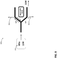
- FIG. 2 illustrates a phase shifter 230 which may be an example of, or included in, any of the phase shifters 130 shown in FIG. 1 , according to some embodiments of the present disclosure.
- the phase shifter 230 may include a first feed line 231 and a second feed line 232.
- An RF input signal 234 may be provided, at an input to the phase shifter 230, to the first feed line 231.
- the feed line 231 may be coupled to a point of the second feed line 232 that is referred to herein as a "coupling point,” so that the RF input signal 234 is split into RF output signals 236-1 and 236-2, which may be provided at two outputs of the phase shifters 230.
- the first feed line 231 may be coupled to a switch arrangement (e.g., a multiplexer) 238 that may include a plurality of switches 240 which may be used to selectively connect the RF input signal 234 to differentcoupling points on the feed line 232 (i.e., the switch arrangement 238 may be used to select one of the locations of the coupling points on the feed line 232 for coupling the first feed line 231 to).
- the switch arrangement 238 may include four switches, shown in FIG. 4 as switches 240-1, 240-2, 240-3, and 240-4, which may be configured to couple the feed line 231 to the feed line 232 at one of the four coupling points 242, shown in FIG.
- Each of the switches 240 may be in one of two states. In a first state (e.g., closed), the switch 240 enables a portion of the RF input signal 234 to be transmitted through the switch, and in a second state (e.g., open), the switch 240 disables transmission of a portion of the RF input signal 234.
- the switch arrangement 238 may be such that, during operation of the phase shifter 230, one of the switches 240 may be closed while the other switches 240 may be open. In this manner, the switch arrangement 238 may couple the RF input signal 234 in the first feed line 231 to the feed line 232 at the coupling point 242 at a location where the switch that is closed is coupled to the feed line 232.
- switches 240 While four switches 240 are shown in FIG. 2 , in other embodiments, any other number of two or more switches 240 may be used. Furthermore, the number of different coupling points 242 does not have to be equal to the number of the switches 240 and, in further embodiments, the switch arrangement 238 may include any number of two or more switches 240 arranged so that the switch arrangement 238 may couple the feed line 231 to the feed line 232 at any of a plurality of different coupling points 242 between the two opposing ends of the feed line 232.
- the feed line 232 may have two branches/portions, which means that the RF input signal 234 enters a split in the feed line 232 at a point where the feed line 231 is coupled to the feed line 232 (i.e., at the coupling point 242).
- the impedance of all branches e.g., of two branches 256-1 and 256-2
- the power of the signal provided by the input 254 may be split evenly.
- the power of the RF input signal 234 may be split evenly, i.e., 50% and 50%, between an RF output signal 236-1 in the first branch 256-1and an RF output signal 236-2 in the second branch 256-2.
- an impedance of the input line 254 to the feed line 232 may be 50 Ohm ( ⁇ ).
- the impedance of each of the branches 256-1 and 256-2 may be set to be equal to a square root of the splitter impedance, e.g., 70.71 ⁇ for a 50 ⁇ splitter. Making the impedance of the splitter to be 50 ⁇ may be desirable in order to avoid impedance mismatch losses. If the two output lines are designed to be 70.71 ⁇ 50 ⁇ 2 , then the impedance looking into the point where the signal splits looks like 50 ⁇ , and so no mismatch losses are introduced.
- FIG. 2 further provides an illustration 260 that shows that a point 262 at which the input line 234 coupled to the feed line 232, thus splitting the feed line 232 into two (or more) branches 256, may be used to define the phase shift realized by each of the branches 256.
- the point 262 at which the RF input signal 234 is provided to the feed line 232 to be split defines the electrical path length that the RF energy of the split signal will travel down each respective path/branch 256 of the feed line splitter, which, in turn, changes the phase shift realized at each output of the feed line splitter.
- a phase shift of 35° may be realized on the branch 256-1 and 105° may be realized on the branch 256-2.
- Each of the branches 256 may be coupled to a respective antenna element 110, as also shown in the illustration 260 of FIG. 2 .
- the length of the feed line 232 may be such that coupling the feed line 231 to one of the predefined locations of the coupling point on the feed line 232 may realize a final phase shift of a certain angle ⁇ for the output RF signal 236-1 from the first branch 256-1 and a phase shift of angle - ⁇ for the output RF signal 236-2 from the first branches 256-2.
- phase shifter 230 if the line length between the feed line connection points is such as to realize a phase shift of 45°, with switch 240-1 on and the others off, ⁇ may be 0°, and - ⁇ may be 0°, if assumed the phase shift is relative to the first or zero phase shift state.
- ⁇ With switch 240-2 on and the others off, ⁇ may be +45°, and - ⁇ may be -45°.
- ⁇ may be +90°, and - ⁇ may be -90°.
- switch 240-4 on and the others off ⁇ may be +135°, and - ⁇ may be -135°. As such the differential nature of the approach is illustrated.
- a single switch 240 can create two differentially phase shifted signals 236-1 and 236-2 from the RF input signal 234.
- a differential phase shift i.e., a phase shift of ⁇ in one branch and a phase shift of - ⁇ in another branch.
- the point at which the RF input signal 234 is fed to the transmission line may be controlled by which one of the switches 240 of the switch arrangement 238 is closed.
- closing the first switch 240-1 may create differential phase shifts of ⁇ 1 and - ⁇ 1 for the output signals 236-1 and 236-2 respectively
- closing the second switch 240-2 may create differential phase shifts of ⁇ 2 and - ⁇ 2 for the output signals 236-1 and 236-2 respectively
- closing the third switch 240-3 may create differential phase shifts of ⁇ 3 and - ⁇ 3 for the output signals 236-1 and 236-2 respectively
- closing the fourth switch 240-4 may create differential phase shifts of ⁇ 4 and - ⁇ 4 for the output signals 236-1 and 236-2 respectively.
- the switch arrangement 238 may be any switching device that may connect an input signal (e.g., the RF input signal 234) to a transmission line (e.g., the feed line 232), where the RF power of the input signal can split into two or more branches, where the connecting point can be changed, differentially phase shifting the signal.
- any one of the switches 240 may be implemented as semiconductor switches (e.g., transistors, SOI devices, PIN diodes, or other semiconductor-based switching elements) or MEMS switches.
- different ones of the switches 240 may be implemented as different types of switches, e.g., one of the switches may be implemented as a PIN diode and another one may be implemented as a MEMS switch.
- a MEMS switch may be implemented as a micrometer-level mechanical movable element which can physically make or break an electrical contact.
- a MEMS switch may have advantages over other RF switching technologies such as PIN, SOI, etc., in terms of the transmission loss, linearity, power handling, and power to drive.
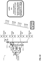
- FIG. 3A provides a schematic illustration of a splitter 340 with two phase shifters 130, each implemented as a switch-based feed line splitter, according to some embodiments of the present disclosure.
- the splitter 340 may be an example of the splitter 140 shown in FIG. 1 , according to some embodiments of the present disclosure.
- the splitter 340 is a 2x switch splitter (i.e., it includes two phase shifters 130).
- the outputs of each of the feed lines of each of the phase shifters 130 may be coupled to different antenna elements 110, as, e.g., was described with reference to the illustration 260 shown in FIG. 2 .
- FIG. 3A provides a schematic illustration of a splitter 340 with two phase shifters 130, each implemented as a switch-based feed line splitter, according to some embodiments of the present disclosure.
- the splitter 340 may be an example of the splitter 140 shown in FIG. 1 , according to some embodiments of the present disclosure.
- the splitter 340 is a 2x switch
- the RF input signal 234 may first be split, e.g., 50/50, among two branches 356-1 and 356-2, and each of the branches 356 may include a corresponding respective phase shifter 130 (shown in FIG. 3A as the phase shifter 130-1 in the branch 356-1 and the phase shifter 130-2 in the branch 356-2).
- the RF signal is then further split into two output signals 236-1 and 236-2, as described with reference to FIG. 2 .
- the power of the RF input signal 234 may be split into 4 RF output signals, each having a quarter of the power of the RF input signal 234.
- the first phase shifter 130-1 may enable provision of an RF signal 236-1 with a phase shift of 2 ⁇ (e.g., 60 degrees) to the antenna element 110-1 and provision of an RF signal 236-2 with a phase shift of -2 ⁇ (e.g., -60 degrees) to the antenna element 110-4.
- the second phase shifter 130-2 may enable provision of an RF signal 236-1 with a phase shift of ⁇ (e.g., 30 degrees) to the antenna element 110-2 and provision of an RF signal 236-2 with a phase shift of - ⁇ (e.g., -30 degrees) to the antenna element 110-3.
- ⁇ and 2 ⁇ nature of the phase shift means that the phase shift created by 130-1 is double 130-2, by virtue of the fact that the feed line length, and/or the line length between switch connection points is twice the length. This relationship where phase shifts of one phase shifter are double that (or, in general, any integer multiple greater than 1) of a phase shifter driving antennae in the same column may be particularly effective for antenna beam steering.
- FIG. 3B provides an example PCB implementation 342 of the splitter 340, according to some embodiments of the present disclosure.
- the PCB layout 342 illustrates an example of PCB Implementation with power splits, impedance transformers and feed line switch splitters, creating 4 phase shifted signals.
- An inset 344 shown in FIG. 3B illustrates example circuit board implementation of the switch arrangement 238, in particular-a switch device with a flip-chip MEMS implementation.
- FIG. 3C provides another view for the PCB implementation 342.
- Implementation 342 including, splitters, quarter wave transformers and switches with feed line splitter, maybe implemented as a standalone module circuit board which is connected both at the input and to the antenna using wire connectors, may also be a subsection of a larger printed circuit board where other circuit elements and sub-circuits may be included.
- FIG. 4 provides a schematic illustration of a splitter 440 with two phase shifters 130 where the switch arrangements 238 of the two phase shifters 130 are implemented on a single die or in a single package, where a package may include any number of die, e.g., mounted on and electrically connected to a metal frame and e.g. encased in plastic, according to some embodiments of the present disclosure.
- the splitter 440 may be an example of the splitter 140 shown in FIG. 1 , according to some embodiments of the present disclosure.
- the splitter 440 shown in FIG. 4 is substantially analogous to that shown in FIG. 3A , the description of which, therefore, is not repeated here in the interests of brevity and only the differences are described.
- the splitter 440 shown in FIG. 4 illustrates that the switch arrangements 238 of the different ones of the phase shifters 130 may be implemented on a single die 438.
- FIG. 4 illustrates that multiple multiplexers may advantageously be put in one package to reduce number of parts required.
- the splitter 440 may be implemented with other variants described herein, such as quarter wave.
- various embodiments with multiple phase shifters, described herein may also be implemented with the switch arrangements 238 of two or more of such phase shifters being implemented on a single die or package as shown in FIG. 4 .
- FIG. 5 provides a schematic illustration of a splitter 540 with three phase shifters 130, each implemented as a switch-based feed line splitter, according to some embodiments of the present disclosure.
- the splitter 540 may be an example of the splitter 140 shown in FIG. 1 , according to some embodiments of the present disclosure.
- the splitter 540 shown in FIG. 5 is substantially analogous to that shown in FIG. 3A , the description of which, therefore, is not repeated here in the interests of brevity and only the differences are described.
- the splitter 540 shown in FIG. 5 illustrates that, instead of splitting the RF input signal 234 2-way as was shown in FIG.
- the RF input signal 234 may be split 3-way, as e.g., shown in FIG. 5 with the 3-way splitting of a 22W RF input signal 234 into 3 signals of about 7W.
- a respective phase shifter 110 is provided, as shown in FIG. 5 .
- 3 phase shifters 130 may be used to drive 6 antenna elements 110, as shown in FIG. 5 , which may provide a higher performing antenna compared to that of FIG. 3A because FIG. 3A illustrated 2 phase shifters 130 driving 4 antenna elements 110.
- FIG. 5 illustrates 3
- the first phase shifter 130-1 may enable provision of an RF signal 236-1 with a phase shift of 5 ⁇ (e.g., 150 degrees) to the antenna element 110-1 and provision of an RF signal 236-2 with a phase shift of -5 ⁇ (e.g., -150 degrees) to the antenna element 110-6;
- the second phase shifter 130-2 may enable provision of an RF signal 236-1 with a phase shift of 3 ⁇ (e.g., 90 degrees) to the antenna element 110-2 and provision of an RF signal 236-2 with a phase shift of -3 ⁇ (e.g., -90 degrees) to the antenna element 110-5;
- the third phase shifter 130-3 may enable provision of an RF signal 236-1 with a phase shift of ⁇ (e.g., 30 degrees) to the antenna element 110-3 and provision of an RF signal 236-2 with a phase shift of - ⁇ (e.g., -30 degrees) to the antenna element 110-4.
- the 3-way splitting as shown in FIG. 5 may enable reducing the number of components within each antenna element 110, as shown in FIG. 5 with each antenna element 110 including 2 components as opposed to that of the antenna elements 110 shown in FIG. 3A with 3 components each.
- the splitter 540 may be implemented with other variants described herein, such as quarter wave and/or single die or package implementation.
- FIG. 6 provides a schematic illustration of two splitters 640-1 and 640-2, each with one phase shifter implemented as a switch-based feed line splitter and with one pass-through path, according to some embodiments of the present disclosure.
- Each of the splitters 640 may be an example of the splitter 140 shown in FIG. 1 , according to some embodiments of the present disclosure.
- the architecture as shown in FIG. 6 may allow doubling the transceivers over a 16-transceiver system (i.e., the embodiment of FIG. 6 may be for 32 transceivers 120, compared to 16 transceivers shown in FIG. 1 ), doubling the control per column. While it may increase the number of parts, it may advantageously enable greater control. In this manner, 2 phase shifters 130 may be used to drive 4 antenna elements 110, as shown in FIG. 6 .
- the splitters 640 may be implemented with other variants described herein, such as quarter wave and/or single die implementation.
- FIG. 7 provides a schematic illustration of a phase shifter 730, implemented as a switch-based feed line splitter, with quarter wave tuning, according to some embodiments of the present disclosure.
- the phase shifter 730 may be an example of the phase shifter 130 shown in FIG. 1 , according to some embodiments of the present disclosure.
- the RF input signal 234 may traverse a quarter wave portion 732 having an impedance of substantially 50 / 2 ⁇ (i.e., substantially 35.5 ⁇ ) before entering the switch arrangement 238.
- the input impedance of the input line 254 may be adjusted from being 50 ⁇ to being 35.5 ⁇ in the quarter wave portion 732 (i.e., the length of the portion 732 is substantially equal to a quarter of a wavelength of the RF input signal 234 and the impedance of the portion 732 is 35.5 ⁇ ).
- the architecture as shown in FIG. 7 may allow achieving optimal loss, shift and power split.
- the 35.5 ⁇ ⁇ /4 impedance transformer at input of the switch arrangement 238 may be used to re-balance the mismatch caused by the splitter branches being formed from two 50 ⁇ branches, thus being substantially lower than 50 ⁇ at the splitting point, leading to mismatch loss.
- the feed line 232 may be created with 50 ⁇ line lengths, with switch contacting lines connected the desired phase shift apart along the feed line. Including such 50 ⁇ line portions may ensure that, as signal passes the feed line 232, it has good return loss.
- the switch arrangement 238 may be made with very low parasitic inductance and capacitance to avoid changing impedance of the 50 ⁇ line 232.
- the phase shifter 730 may be in one of 4 states, as shown with an inset 750 shown in FIG. 7 .
- quarter wave portions may be used after the RF input signal 234 is split, as shown in FIG. 8 , providing an illustration of a splitter 840 with a quarter wave switching principle, according to some embodiments of the present disclosure.
- the splitter 840 may be an example of the splitter 140 shown in FIG. 1 , according to some embodiments of the present disclosure.
- the RF input signal 234 may enters the splitter 840, where it may be split substantially equally between all branches of the split, e.g., it may split 50/50 between two branches. As shown in FIG. 8 , in each branch of the split, one quarter wavelength distance away from the splitting point, there may be a switch to ground - shown as a switch 842-1 in the first branch and a switch 842-2 in the second branch. Consider that one switch is closed (e.g., the switch 842-1) and the other one is open (e.g., the switch 842-2).
- the switch 842-1 when the switch 842-1 is closed, the power of the RF input signal 234 that traverses this branch (i.e., 50% of the power of the RF input signal 234 in this example) may reflect from the switch 842-1 and will undergo a 180 degree phase shift transformation, so the switch 842-1 will appear to the RF input signal as an open circuit.
- the switch 842-2 when the switch 842-2 is open, the power of the RF input signal 234 that traverses this branch (i.e., 50% of the power of the RF input signal 234 in this example) will not see the switch 842-2 and pass through, as shown in FIG. 8 .
- FIG. 8 illustrates an example with a 2-way power split (i.e., there are two branches over which the RF input signal 234 is split), descriptions provided with reference to FIG. 8 may be easily extended to embodiments of any N-way power split, where N is an integer greater than 1.
- N-1 switches with connection to ground may be closed and 1 switch with connection to ground may be open, and the split power of the RF input signal 234 will then traverse the branch with the open switch, similar to the example of the lower branch shown in FIG. 8 .
- FIG. 9 provides a schematic illustration of a splitter 940 with two switch-based feed line splitter phase shifters with quarter wave and switch to ground implementation, according to some embodiments of the present disclosure.
- the splitter 940 may be an example of the splitter 140 shown in FIG. 1 , according to some embodiments of the present disclosure.
- the splitter 940 shown in FIG. 9 is substantially analogous to that shown in FIG. 3A , the description of which, therefore, is not repeated here in the interests of brevity and only the differences are described.
- a switch arrangement 938-1 of the phase shifter 130-1 and a switch arrangement 938-2 of the phase shifter 130-2) are configured to implement a quarter wave switching principle as shown in FIG. 8 but for the example of a 4-way power split (as opposed to a 2-way split shown in FIG. 8 ).
- 3 switches with connection to ground may be closed and 1 switch with connection to ground may be open, and the split power of the RF input signal 234 will then traverse the branch with the open switch, resulting in the split power of the RF input signal 234 traversing the branch with the open switch.
- each of the phase shifters 130 of the splitter 940 may be in one of 4 states, as shown with an inset 950 shown in FIG. 9 .
- FIG. 10 provides a schematic illustration of a splitter 1040 with two switch-based feed line splitter phase shifters with quarter wave and without switch to ground implementation, according to some embodiments of the present disclosure.
- the splitter 1040 may be an example of the splitter 140 shown in FIG. 1 , according to some embodiments of the present disclosure.
- the splitter 1040 shown in FIG. 10 is substantially analogous to that shown in FIG. 3A , the description of which, therefore, is not repeated here in the interests of brevity and only the differences are described.
- FIG. 10 illustrates that, in some embodiments, each of multiple, e.g., 2, branches 1056 over which the RF input signal 234 may be split (namely, a first branch 1056-1 and a second branch 1056-2 shown in FIG.
- the 10 for the example of 2 branches may include a quarter wave portion 1002 with a 70.71 ⁇ (50V2) impedance, followed by another quarter wave portion 1004 but now with a 35.5 ⁇ (50/V2) impedance, before the RF signal in the branch is split further by the corresponding switch arrangement 338 of the branch.
- the values of the impedance of the two quarter wave portions 1002 and 1004 may be selected in order to create an impedance transformation, where a line of length one quarter the wavelength and at (50/V2) or 35.5 ⁇ is transformed to 50 ⁇ at the end of the quarter wave line. Likewise, where a line of length one quarter the wavelength and at (50V2) or 70.71 ⁇ is transformed to 50 ⁇ at the end of the quarter wavelength line.
- these values may be any value(s) suitable for re-balancing the mismatch in impedance created by the mismatch at the splitter, which can be any one of numerous line lengths, impedance values and circuit elements such as capacitances or inductances.
- FIG. 11 provides a schematic illustration of a phase shifter 1130, implemented as a switch-based feed line splitter, with quarter wave tuning and switches to ground implementation, according to some embodiments of the present disclosure.
- the phase shifter 1130 may be an example of the phase shifter 130 shown in FIG. 1 , according to some embodiments of the present disclosure.
- the phase shifter 1130 shown in FIG. 11 is substantially analogous to that shown in FIG. 7 , the description of which, therefore, is not repeated here in the interests of brevity and only the differences are described.
- FIG. 11 illustrates that, in some embodiments, the RF input signal 234 may traverse a portion 1132 which is substantially similar to the portion 732 shown in FIG.
- FIG. 11 illustrates that, in some embodiments, a switch arrangement 1138 (substantially similar to the switch arrangement 238) may include a plurality of switches 1140 (substantially similar to the switches 240), but each configured so that it may be connected to the ground using a further switch (referred to as "ground switch") 1142. Only one of the switches 1140 and one of the ground switches 1142 are labeled in FIG. 11 with reference numerals in order to not clutter the drawing, but 4 of such switches 1140 and ground switches 1142 are shown in the example of FIG. 11 .
- the switches 1140 operate as described with reference to the switches 240 shown in FIG. 2
- the ground switches 1142 operate as described with reference to the switches 842 shown in FIG. 8 but shown in FIG. 11 for the example of a 4-way power split (as opposed to a 2-way split shown in FIG. 8 ).
- one of the switches 1140 may be closed (with all other of the switches 1140 being open) and a corresponding ground switch 1142 may then be open, resulting in the split portion of the RF input signal 234 traversing that branch of the switch arrangement 1138.
- the remaining ground switches 1142 may be either closed or open, which does not matter because the switches 1140 of those remaining ground switches 1142 are open, so no RF signal traverses those branches.
- FIG. 11 is similar to FIG. 3A but this time using quarter wave feed lines, with a shorting switch associated with each of the switches 240.
- the ground switch 1142 may make the feed line look like an open when the channel is not being used.
- FIG. 11 further illustrates that the portions connecting each one of the ground switches 1142 to the feed line 232 may be quarter wave portions 1144 (only one of which is labelled in FIG. 11 with the reference numeral 1144 in order to not clutter the drawing).
- the inset 1150 shown in FIG. 11 illustrates one example of a PCB implementation of the phase shifter 1130.
- FIG. 12 provides a schematic illustration of a phase shifter 1230, implemented as a switch-based feed line splitter, with quarter wave and switch to ground implementation, according to some embodiments of the present disclosure.
- the phase shifter 1230 may be an example of the phase shifter 130 shown in FIG. 1 , according to some embodiments of the present disclosure.
- the phase shifter 1230 shown in FIG. 12 is substantially analogous to any one of the two phase shifters 938 shown in FIG. 9 , the description of which, therefore, is not repeated here in the interests of brevity and only the differences are described.
- FIG. 12 illustrates that, in some embodiments, the phase shifter 1230 may be configured to drive 4 antenna elements with one die or package, where previous embodiments drove 2 antenna elements.
- this implementation may use quarter wave switch implementation at the input side as used in FIG. 9 , while at the output of the switch, the signal is split again and two quarter wave lines connect to 2 feed lines, 1232-1 and 1232-2, of differing lengths.
- the quarter wave lines from the switch to the feed lines may both be terminated to ground quarter wave at the switch, thus making efficient use of this grounding element.
- one 4 channel multiplexer may be configured to drive 4 antenna elements with differing and differential phase shifts, where previous embodiments were driving 2 antenna elements.
- FIG. 13 provides a schematic illustration of ESD protection with a shunt inductor 1302, according to some embodiments of the present disclosure.
- the inductor 1302 may be coupled to ground, ensuring that it has high impedance at the operating frequency.
- Such an inductor may be configured to short to ground in case of any ESD zaps.
- Such an inductor/structure may, optionally, be added to any of the nodes 236 or 234 shown in FIG. 2 , specifically the feed from the previous stage such as the power amplifier or the output nodes which drive the antenna elements.
- FIG. 13 shows a portion of the circuit layout as shown in FIGS. 3B and 3C , described above.
- FIG. 14 provides a schematic illustration of ESD protection with a quarter wave stub 1402, according to some embodiments of the present disclosure.
- the quarter wave stub 1402 may be coupled to ground at the operating frequency.
- Such a quarter wave stub 1402 may, optionally, be added to any of the nodes 236 or 234 shown in FIG. 2 , specifically the feed from the previous stage such as the power amplifier or the output nodes which drive the antenna elements.
- FIG. 14 One example of using the quarter wave stub 1402 is shown in FIG. 14 with an illustration 1410, where the illustration 1410 shows a portion of the circuit layout as shown in FIGS. 3B and 3C , described above.
- FIG. 15 provides a schematic illustration of a stub bandstop filter 1502, according to some embodiments of the present disclosure.
- the stub bandstop filter 1502 may be placed on a feed line, with the length of the stub being a quarter wave at the frequency that is desired to filter.
- Such a stub bandstop filter 1502 may, optionally, be added to any of the nodes 236 or 234 shown in FIG. 2 , specifically the feed from the previous stage such as the power amplifier or the output nodes which drive the antenna elements.
- FIG. 15 One example of using the stub bandstop filter 1502 is shown in FIG. 15 with an illustration 1510, where the illustration 1510 shows a portion of the circuit layout as shown in FIGS. 3B and 3C , described above.
- FIG. 16 provides a schematic illustration of a stub bandpass filter 1602, according to some embodiments of the present disclosure.
- the stub bandpass filter 1602 may be placed on a feed line, with the length of the stub being a quarter wave at the frequency at which it is desired to operate, thereby reducing or altogether removing undesirable signals at other frequencies.
- Such a stub bandpass filter 1602 may, optionally, be added to any of the nodes 236 or 234 shown in FIG. 2 , specifically the feed from the previous stage such as the power amplifier or the output nodes which drive the antenna elements.
- FIG. 16 One example of using the stub bandpass filter 1602 is shown in FIG. 16 with an illustration 1610, where the illustration 1610 shows a portion of the circuit layout as shown in FIGS. 3B and 3C , described above.
- FIG. 17 provides a block diagram illustrating an example data processing system 1700 that may be configured to implement, or control implementations of, at least portions of phase shifters using switch-based feed line splitters as described herein, according to some embodiments of the present disclosure.
- the data processing system 1700 may include at least one processor 1702, e.g. a hardware processor 1702, coupled to memory elements 1704 through a system bus 1706. As such, the data processing system may store program code within memory elements 1704. Further, the processor 1702 may execute the program code accessed from the memory elements 1704 via a system bus 1706. In one aspect, the data processing system may be implemented as a computer that is suitable for storing and/or executing program code. It should be appreciated, however, that the data processing system 1700 may be implemented in the form of any system including a processor and a memory that is capable of performing the functions described within this disclosure.
- the processor 1702 can execute software or an algorithm to perform the activities as discussed in this specification, in particular activities related to realizing phase shifters using switch-based feed line splitters as described herein.
- the processor 1702 may include any combination of hardware, software, or firmware providing programmable logic, including by way of nonlimiting example a microprocessor, a digital signal processor (DSP), a field-programmable gate array (FPGA), a programmable logic array (PLA), an application specific integrated circuit (IC) (ASIC), or a virtual machine processor.
- the processor 1702 may be communicatively coupled to the memory element 1704, for example in a direct-memory access (DMA) configuration, so that the processor 1702 may read from or write to the memory elements 1704.
- DMA direct-memory access
- the memory elements 1704 may include any suitable volatile or non-volatile memory technology, including double data rate (DDR) random access memory (RAM), synchronous RAM (SRAM), dynamic RAM (DRAM), flash, read-only memory (ROM), optical media, virtual memory regions, magnetic or tape memory, or any other suitable technology.
- DDR double data rate
- SRAM synchronous RAM
- DRAM dynamic RAM
- flash read-only memory
- any of the memory elements discussed herein should be construed as being encompassed within the broad term "memory.”
- the information being measured, processed, tracked or sent to or from any of the components of the data processing system 1700 could be provided in any database, register, control list, cache, or storage structure, all of which can be referenced at any suitable timeframe. Any such storage options may be included within the broad term "memory" as used herein.
- any of the potential processing elements, modules, and machines described herein should be construed as being encompassed within the broad term "processor.”
- Each of the elements shown in the presentfigures e.g., any of the circuits/components shown in FIGS. 1-16 , can also include suitable interfaces for receiving, transmitting, and/or otherwise communicating data or information in a network environment so that they can communicate with, e.g., the data processing system 1700 of another one of these elements.
- mechanisms for implementing phase shifters using switch-based feed line splitters as outlined herein may be implemented by logic encoded in one or more tangible media, which may be inclusive of non-transitory media, e.g., embedded logic provided in an ASIC, in DSP instructions, software (potentially inclusive of object code and source code) to be executed by a processor, or other similar machine, etc.
- memory elements such as e.g. the memory elements 1704 shown in FIG. 17 , can store data or information used for the operations described herein. This includes the memory elements being able to store software, logic, code, or processor instructions that are executed to carry out the activities described herein.
- a processor can execute any type of instructions associated with the data or information to achieve the operations detailed herein.
- the processors such as e.g. the processor1702 shown in FIG. 17 , could transform an element or an article (e.g., data) from one state or thing to another state or thing.
- the activities outlined herein may be implemented with fixed logic or programmable logic (e.g., software/computer instructions executed by a processor) and the elements identified herein could be some type of a programmable processor, programmable digital logic (e.g., an FPGA, a DSP, an erasable programmable read-only memory (EPROM), an electrically erasable programmable read-only memory (EEPROM)) or an ASIC that includes digital logic, software, code, electronic instructions, or any suitable combination thereof.
- programmable digital logic e.g., an FPGA, a DSP, an erasable programmable read-only memory (EPROM), an electrically erasable programmable read-only memory (EEPROM)
- ASIC that includes digital logic, software, code, electronic instructions, or any suitable combination thereof.
- the memory elements 1704 may include one or more physical memory devices such as, for example, local memory 1708 and one or more bulk storage devices 1710.
- the local memory may refer to RAM or other non-persistent memory device(s) generally used during actual execution of the program code.
- a bulk storage device may be implemented as a hard drive or other persistent data storage device.
- the processing system 1700 may also include one or more cache memories (not shown) that provide temporary storage of at least some program code in order to reduce the number of times program code must be retrieved from the bulk storage device 1710 during execution.
- the memory elements 1704 may store an application 1718.
- the application 1718 may be stored in the local memory 1708, the one or more bulk storage devices 1710, or apart from the local memory and the bulk storage devices.
- the data processing system 1700 may further execute an operating system (not shown in FIG. 17 ) that can facilitate execution of the application 1718.
- the application 1718 being implemented in the form of executable program code, can be executed by the data processing system 1700, e.g., by the processor 1702. Responsive to executing the application, the data processing system 1700 may be configured to perform one or more operations or method steps described herein.
- I/O devices depicted as an input device 1712 and an output device 1714 can be coupled to the data processing system.
- input devices may include, but are not limited to, a keyboard, a pointing device such as a mouse, or the like.
- output devices may include, but are not limited to, a monitor or a display, speakers, or the like.
- the output device 1714 may be any type of screen display, such as plasma display, liquid crystal display (LCD), organic light emitting diode (OLED) display, electroluminescent (EL) display, or any other indicator, such as a dial, barometer, or LEDs.
- the system may include a driver (not shown) for the output device 1714.
- Input and/or output devices 1712, 1714 may be coupled to the data processing system either directly or through intervening I/O controllers.
- the input and the output devices may be implemented as a combined input/output device (illustrated in FIG. 17 with a dashed line surrounding the input device 1712 and the output device 1714).
- a combined device is a touch sensitive display, also sometimes referred to as a "touch screen display” or simply "touch screen”.
- input to the device may be provided by a movement of a physical object, such as e.g. a stylus or a finger of a user, on or near the touch screen display.
- a network adapter 1716 may also, optionally, be coupled to the data processing system to enable it to become coupled to other systems, computer systems, remote network devices, and/or remote storage devices through intervening private or public networks.
- the network adapter may comprise a data receiver for receiving data that is transmitted by said systems, devices and/or networks to the data processing system 1700, and a data transmitter for transmitting data from the data processing system 1700 to said systems, devices and/or networks.
- Modems, cable modems, and Ethernet cards are examples of different types of network adapterthat may be used with the data processing system 1700.
- the features discussed herein can be applicable to automotive systems, medical systems, scientific instrumentation, wireless and wired communications, radio, radar, and digital-processing-based systems.
- phase shifters components of a system, such as phase shifters, frequency mixers, amplifiers, and/or other components can readily be replaced, substituted, or otherwise modified in order to accommodate particular circuitry needs.
- phase shifters frequency mixers, amplifiers, and/or other components
- other components can readily be replaced, substituted, or otherwise modified in order to accommodate particular circuitry needs.
- complementary electronic devices, hardware, software, etc. offer an equally viable option for implementing the teachings of the present disclosure related to phase shifters using switch-based feed line splitters as described herein.
- Parts of various systems for implementing phase shifters using switch-based feed line splitters as proposed herein can include electronic circuitry to perform the functions described herein.
- one or more parts of the system can be provided by a processor specially configured for carrying out the functions described herein.
- the processor may include one or more application specific components, or may include programmable logic gates which are configured to carry out the functions describe herein.
- the circuitry can operate in analog domain, digital domain, or in a mixed-signal domain.
- the processor may be configured to carrying out the functions described herein by executing one or more instructions stored on a non-transitory computer-readable storage medium.
- any number of electrical circuits of the present figures may be implemented on a board of an associated electronic device.
- the board can be a general circuit board that can hold various components of the internal electronic system of the electronic device and, further, provide connectors for other peripherals. More specifically, the board can provide the electrical connections by which the other components of the system can communicate electrically.
- Any suitable processors (inclusive of DSPs, microprocessors, supporting chipsets, etc.), computer-readable non-transitory memory elements, etc. can be suitably coupled to the board based on particular configuration needs, processing demands, computer designs, etc.
- Other components such as external storage, additional sensors, controllers for audio/video display, and peripheral devices may be attached to the board as plug-in cards, via cables, or integrated into the board itself.
- the functionalities described herein may be implemented in emulation form as software or firmware running within one or more configurable (e.g., programmable) elements arranged in a structure that supports these functions.
- the software or firmware providing the emulation may be provided on non-transitory computer-readable storage medium comprising instructions to allow a processor to carry out those functionalities.
- the electrical circuits of the present figures may be implemented as stand-alone modules (e.g., a device with associated components and circuitry configured to perform a specific application or function) or implemented as plug-in modules into application specific hardware of electronic devices.
- SOC system on chip
- An SOC represents an IC that integrates components of a computer or other electronic system into a single chip. It may contain digital, analog, mixed-signal, and often RF functions: all of which may be provided on a single chip substrate.
- MCM multi-chip-module
- ASICs Application Specific Integrated Circuits
- FPGAs Field Programmable Gate Arrays
Landscapes
- Variable-Direction Aerials And Aerial Arrays (AREA)
Applications Claiming Priority (2)
| Application Number | Priority Date | Filing Date | Title |
|---|---|---|---|
| CN2019093016 | 2019-06-26 | ||
| US16/869,827 US11489255B2 (en) | 2019-06-26 | 2020-05-08 | Phase shifters using switch-based feed line splitters |
Publications (1)
| Publication Number | Publication Date |
|---|---|
| EP3758134A1 true EP3758134A1 (de) | 2020-12-30 |
Family
ID=71138699
Family Applications (1)
| Application Number | Title | Priority Date | Filing Date |
|---|---|---|---|
| EP20181923.2A Pending EP3758134A1 (de) | 2019-06-26 | 2020-06-24 | Phasenschieber unter verwendung von schaltbasierten speiseleitungsteilern |
Country Status (2)
| Country | Link |
|---|---|
| EP (1) | EP3758134A1 (de) |
| CN (1) | CN112151964A (de) |
Families Citing this family (5)
| Publication number | Priority date | Publication date | Assignee | Title |
|---|---|---|---|---|
| CN111525215B (zh) * | 2020-05-06 | 2021-11-16 | 湖南时变通讯科技有限公司 | 移相单元、天线单元、相控阵列单元以及相控阵列 |
| US11411293B1 (en) * | 2021-09-10 | 2022-08-09 | Nanotronics Imaging, Inc. | Fault protected signal splitter apparatus |
| US11894596B2 (en) | 2021-09-10 | 2024-02-06 | Nanotronics Imaging, Inc. | Fault protected signal splitter apparatus |
| WO2023092567A1 (en) * | 2021-11-29 | 2023-06-01 | Telefonaktiebolaget Lm Ericsson (Publ) | Antenna filter unit (afu), radio unit (ru), and communication device |
| CN114744383B (zh) * | 2022-05-30 | 2023-12-01 | 南京邮电大学 | 共面波导结构的低损耗单开关宽带微波180度移相器 |
Citations (5)
| Publication number | Priority date | Publication date | Assignee | Title |
|---|---|---|---|---|
| EP1898523A1 (de) * | 2006-09-05 | 2008-03-12 | Alcatel Lucent | Schaltbarer Leistungsteiler und Leistungsverstärkermodul |
| US7595753B2 (en) * | 2007-03-30 | 2009-09-29 | Sony Deutschland Gmbh | Broadband beam steering antenna |
| WO2016150483A1 (en) * | 2015-03-23 | 2016-09-29 | Fraunhofer-Gesellschaft zur Förderung der angewandten Forschung e.V. | Phase shifter |
| US9780448B1 (en) * | 2013-09-30 | 2017-10-03 | The United States Of America As Represented By Secretary Of The Navy | True path beam steering |
| EP3386029A1 (de) * | 2017-04-07 | 2018-10-10 | Honeywell International Inc. | Phasenschieber mit niedriger dispersion auf basis eines modifizierten hybriden ringleistungsteilers |
Family Cites Families (4)
| Publication number | Priority date | Publication date | Assignee | Title |
|---|---|---|---|---|
| US9871293B2 (en) * | 2010-11-03 | 2018-01-16 | The Boeing Company | Two-dimensionally electronically-steerable artificial impedance surface antenna |
| CN105281030A (zh) * | 2015-09-29 | 2016-01-27 | 天津工业大学 | 一种新型rfid平面阵列天线馈电网络 |
| US10263330B2 (en) * | 2016-05-26 | 2019-04-16 | Nokia Solutions And Networks Oy | Antenna elements and apparatus suitable for AAS calibration by selective couplerline and TRX RF subgroups |
| CN109638391B (zh) * | 2018-11-09 | 2020-07-07 | 华南理工大学 | 介质移动式移相器及基站天线 |
-
2020
- 2020-06-24 EP EP20181923.2A patent/EP3758134A1/de active Pending
- 2020-06-28 CN CN202010597664.6A patent/CN112151964A/zh active Pending
Patent Citations (5)
| Publication number | Priority date | Publication date | Assignee | Title |
|---|---|---|---|---|
| EP1898523A1 (de) * | 2006-09-05 | 2008-03-12 | Alcatel Lucent | Schaltbarer Leistungsteiler und Leistungsverstärkermodul |
| US7595753B2 (en) * | 2007-03-30 | 2009-09-29 | Sony Deutschland Gmbh | Broadband beam steering antenna |
| US9780448B1 (en) * | 2013-09-30 | 2017-10-03 | The United States Of America As Represented By Secretary Of The Navy | True path beam steering |
| WO2016150483A1 (en) * | 2015-03-23 | 2016-09-29 | Fraunhofer-Gesellschaft zur Förderung der angewandten Forschung e.V. | Phase shifter |
| EP3386029A1 (de) * | 2017-04-07 | 2018-10-10 | Honeywell International Inc. | Phasenschieber mit niedriger dispersion auf basis eines modifizierten hybriden ringleistungsteilers |
Also Published As
| Publication number | Publication date |
|---|---|
| CN112151964A (zh) | 2020-12-29 |
Similar Documents
| Publication | Publication Date | Title |
|---|---|---|
| EP3758134A1 (de) | Phasenschieber unter verwendung von schaltbasierten speiseleitungsteilern | |
| US11489255B2 (en) | Phase shifters using switch-based feed line splitters | |
| US11652524B2 (en) | Antenna system for a multi-beam beamforming front-end wireless transceiver | |
| TWI713570B (zh) | 關於孔隙來配置的多個天線 | |
| EP3751732A1 (de) | Koppeln einer vorspannungsschaltung mit einem verstärker unter verwendung einer adaptiven kopplungsanordnung | |
| EP3713081B1 (de) | Phasenverschiebungsmodul mit verbessertem frequenzvervielfacher und temperaturkompensation in lokalem oszillatorweg | |
| EP4020801B1 (de) | Verstärker mit variabler verstärkung mit kreuzkopplungsschaltanordnungen | |
| CN114172472B (zh) | 用于载波聚合的无线放大器电路 | |
| US20210194122A1 (en) | Antenna device and wireless communication device | |
| EP3430672B1 (de) | Magnetisch-induktiver wellenleiter | |
| US20240055765A1 (en) | Circularly-polarized antennas with wide scanning ranges | |
| US20230261392A1 (en) | Dual wideband orthogonally polarized antenna | |
| Chang et al. | Reflection-type phase shifter integrated with tunable power attenuation mechanism for sub-6 GHz wireless applications | |
| CN113904646A (zh) | 一种低功耗宽带无源移相器及相控阵装置 | |
| US11670851B2 (en) | Non-uniformly thinned half-duplex phased arrays with dual-band antenna elements | |
| US20240097728A1 (en) | Active Power Splitter and Combiner Circuitry | |
| US20230231295A1 (en) | Electronic device | |
| US20240088836A1 (en) | Radio-frequency Circuitry with Shapable Differential Coupled Lines for Low-loss Impedance Matching | |
| US20240178567A1 (en) | Antenna module and communication apparatus equipped with the same | |
| Rohrdantz et al. | A frequency and polarization reconfigurable patch antenna at K-band | |
| CN117749131A (zh) | 有源功率分离器和组合器电路 | |
| Rahman et al. | ESPAR array design for the wireless communication and IoT applications | |
| Nawaz et al. | Design, implementation and experimental comparison between two dual polarized 2.4 GHz microstrip patch antennas | |
| CN117118476A (zh) | 具有带有频率选择性滤波的可重新配置的多线圈变压器的电子设备 |
Legal Events
| Date | Code | Title | Description |
|---|---|---|---|
| PUAI | Public reference made under article 153(3) epc to a published international application that has entered the european phase |
Free format text: ORIGINAL CODE: 0009012 |
|
| STAA | Information on the status of an ep patent application or granted ep patent |
Free format text: STATUS: THE APPLICATION HAS BEEN PUBLISHED |
|
| AK | Designated contracting states |
Kind code of ref document: A1 Designated state(s): AL AT BE BG CH CY CZ DE DK EE ES FI FR GB GR HR HU IE IS IT LI LT LU LV MC MK MT NL NO PL PT RO RS SE SI SK SM TR |
|
| AX | Request for extension of the european patent |
Extension state: BA ME |
|
| STAA | Information on the status of an ep patent application or granted ep patent |
Free format text: STATUS: REQUEST FOR EXAMINATION WAS MADE |
|
| 17P | Request for examination filed |
Effective date: 20210624 |
|
| RBV | Designated contracting states (corrected) |
Designated state(s): AL AT BE BG CH CY CZ DE DK EE ES FI FR GB GR HR HU IE IS IT LI LT LU LV MC MK MT NL NO PL PT RO RS SE SI SK SM TR |
|
| RIC1 | Information provided on ipc code assigned before grant |
Ipc: H03H 7/18 20060101ALN20221219BHEP Ipc: H03H 7/21 20060101ALN20221219BHEP Ipc: H01Q 3/38 20060101ALI20221219BHEP Ipc: H01P 1/18 20060101AFI20221219BHEP |
|
| STAA | Information on the status of an ep patent application or granted ep patent |
Free format text: STATUS: EXAMINATION IS IN PROGRESS |
|
| 17Q | First examination report despatched |
Effective date: 20230217 |