EP3758071A1 - Structures for fabrication of solar cells - Google Patents
Structures for fabrication of solar cells Download PDFInfo
- Publication number
- EP3758071A1 EP3758071A1 EP20190231.9A EP20190231A EP3758071A1 EP 3758071 A1 EP3758071 A1 EP 3758071A1 EP 20190231 A EP20190231 A EP 20190231A EP 3758071 A1 EP3758071 A1 EP 3758071A1
- Authority
- EP
- European Patent Office
- Prior art keywords
- solar cell
- type diffusion
- type
- diffusion regions
- laser
- Prior art date
- Legal status (The legal status is an assumption and is not a legal conclusion. Google has not performed a legal analysis and makes no representation as to the accuracy of the status listed.)
- Granted
Links
Images





Classifications
-
- H—ELECTRICITY
- H10—SEMICONDUCTOR DEVICES; ELECTRIC SOLID-STATE DEVICES NOT OTHERWISE PROVIDED FOR
- H10F—INORGANIC SEMICONDUCTOR DEVICES SENSITIVE TO INFRARED RADIATION, LIGHT, ELECTROMAGNETIC RADIATION OF SHORTER WAVELENGTH OR CORPUSCULAR RADIATION
- H10F77/00—Constructional details of devices covered by this subclass
- H10F77/30—Coatings
- H10F77/306—Coatings for devices having potential barriers
- H10F77/311—Coatings for devices having potential barriers for photovoltaic cells
- H10F77/315—Coatings for devices having potential barriers for photovoltaic cells the coatings being antireflective or having enhancing optical properties
-
- H—ELECTRICITY
- H10—SEMICONDUCTOR DEVICES; ELECTRIC SOLID-STATE DEVICES NOT OTHERWISE PROVIDED FOR
- H10F—INORGANIC SEMICONDUCTOR DEVICES SENSITIVE TO INFRARED RADIATION, LIGHT, ELECTROMAGNETIC RADIATION OF SHORTER WAVELENGTH OR CORPUSCULAR RADIATION
- H10F10/00—Individual photovoltaic cells, e.g. solar cells
-
- H—ELECTRICITY
- H10—SEMICONDUCTOR DEVICES; ELECTRIC SOLID-STATE DEVICES NOT OTHERWISE PROVIDED FOR
- H10F—INORGANIC SEMICONDUCTOR DEVICES SENSITIVE TO INFRARED RADIATION, LIGHT, ELECTROMAGNETIC RADIATION OF SHORTER WAVELENGTH OR CORPUSCULAR RADIATION
- H10F10/00—Individual photovoltaic cells, e.g. solar cells
- H10F10/10—Individual photovoltaic cells, e.g. solar cells having potential barriers
- H10F10/14—Photovoltaic cells having only PN homojunction potential barriers
- H10F10/146—Back-junction photovoltaic cells, e.g. having interdigitated base-emitter regions on the back side
-
- H—ELECTRICITY
- H10—SEMICONDUCTOR DEVICES; ELECTRIC SOLID-STATE DEVICES NOT OTHERWISE PROVIDED FOR
- H10F—INORGANIC SEMICONDUCTOR DEVICES SENSITIVE TO INFRARED RADIATION, LIGHT, ELECTROMAGNETIC RADIATION OF SHORTER WAVELENGTH OR CORPUSCULAR RADIATION
- H10F71/00—Manufacture or treatment of devices covered by this subclass
- H10F71/121—The active layers comprising only Group IV materials
-
- H—ELECTRICITY
- H10—SEMICONDUCTOR DEVICES; ELECTRIC SOLID-STATE DEVICES NOT OTHERWISE PROVIDED FOR
- H10F—INORGANIC SEMICONDUCTOR DEVICES SENSITIVE TO INFRARED RADIATION, LIGHT, ELECTROMAGNETIC RADIATION OF SHORTER WAVELENGTH OR CORPUSCULAR RADIATION
- H10F77/00—Constructional details of devices covered by this subclass
- H10F77/20—Electrodes
- H10F77/206—Electrodes for devices having potential barriers
- H10F77/211—Electrodes for devices having potential barriers for photovoltaic cells
- H10F77/219—Arrangements for electrodes of back-contact photovoltaic cells
-
- Y—GENERAL TAGGING OF NEW TECHNOLOGICAL DEVELOPMENTS; GENERAL TAGGING OF CROSS-SECTIONAL TECHNOLOGIES SPANNING OVER SEVERAL SECTIONS OF THE IPC; TECHNICAL SUBJECTS COVERED BY FORMER USPC CROSS-REFERENCE ART COLLECTIONS [XRACs] AND DIGESTS
- Y02—TECHNOLOGIES OR APPLICATIONS FOR MITIGATION OR ADAPTATION AGAINST CLIMATE CHANGE
- Y02E—REDUCTION OF GREENHOUSE GAS [GHG] EMISSIONS, RELATED TO ENERGY GENERATION, TRANSMISSION OR DISTRIBUTION
- Y02E10/00—Energy generation through renewable energy sources
- Y02E10/50—Photovoltaic [PV] energy
- Y02E10/52—PV systems with concentrators
-
- Y—GENERAL TAGGING OF NEW TECHNOLOGICAL DEVELOPMENTS; GENERAL TAGGING OF CROSS-SECTIONAL TECHNOLOGIES SPANNING OVER SEVERAL SECTIONS OF THE IPC; TECHNICAL SUBJECTS COVERED BY FORMER USPC CROSS-REFERENCE ART COLLECTIONS [XRACs] AND DIGESTS
- Y02—TECHNOLOGIES OR APPLICATIONS FOR MITIGATION OR ADAPTATION AGAINST CLIMATE CHANGE
- Y02E—REDUCTION OF GREENHOUSE GAS [GHG] EMISSIONS, RELATED TO ENERGY GENERATION, TRANSMISSION OR DISTRIBUTION
- Y02E10/00—Energy generation through renewable energy sources
- Y02E10/50—Photovoltaic [PV] energy
- Y02E10/547—Monocrystalline silicon PV cells
-
- Y—GENERAL TAGGING OF NEW TECHNOLOGICAL DEVELOPMENTS; GENERAL TAGGING OF CROSS-SECTIONAL TECHNOLOGIES SPANNING OVER SEVERAL SECTIONS OF THE IPC; TECHNICAL SUBJECTS COVERED BY FORMER USPC CROSS-REFERENCE ART COLLECTIONS [XRACs] AND DIGESTS
- Y02—TECHNOLOGIES OR APPLICATIONS FOR MITIGATION OR ADAPTATION AGAINST CLIMATE CHANGE
- Y02P—CLIMATE CHANGE MITIGATION TECHNOLOGIES IN THE PRODUCTION OR PROCESSING OF GOODS
- Y02P70/00—Climate change mitigation technologies in the production process for final industrial or consumer products
- Y02P70/50—Manufacturing or production processes characterised by the final manufactured product
Definitions
- Embodiments of the subject matter described herein relate generally to solar cells. More particularly, embodiments of the subject matter relate to solar cell fabrication processes and structures.
- Solar cells are well known devices for converting solar radiation to electrical energy. They may be fabricated on a semiconductor wafer using semiconductor processing technology.
- a solar cell includes P-type and N-type diffusion regions. Solar radiation impinging on the solar cell creates electrons and holes that migrate to the diffusion regions, thereby creating voltage differentials between the diffusion regions.
- BCBJ back junction
- the P-type and N-type diffusion regions and the metal contacts coupled to them are on the backside of the solar cell. The metal contacts allow an external electrical circuit to be coupled to and be powered by the solar cell.
- cell parameters such as shunt resistance, series resistance, and bulk lifetime are important parameters to maintain on the final fabricated devices.
- Solar cell process steps in particular laser ablation steps on BCBJ solar cells, may impact each of these parameters.
- Post laser losses due to series resistance or lifetime maybe be offset at the expense of step cost, such as by adding thermal or etching steps.
- an added complication of shunting on high-efficiency BCBJ solar cells may be prevalent when the cell architecture has metal of one polarity over diffusions of another polarity.
- Embodiments of the present invention pertain to novel solar cell fabrication processes and structures that reduce the cost of solar cell fabrication and improve solar cell reliability.
- contact holes of solar cells are formed by laser ablation to accommodate various solar cell designs.
- Use of a laser to form the contact holes is facilitated by replacing films formed on the diffusion regions with a film that has substantially uniform thickness.
- the film thickness as absorption may be tailored to match laser parameters. Dopant depth underneath contact holes may be controlled to increase the laser ablation process margins.
- the laser configuration may be tailored to form contact holes through dielectric films of varying thicknesses.
- metal contacts for one polarity of diffusion region may run over an opposite polarity diffusion region (e.g., metal contact for an N-type diffusion region formed over a P-type diffusion region).
- metal contact for an N-type diffusion region formed over a P-type diffusion region it is critical that the interlayer dielectric that electrically insulates the metal contacts from the diffusion regions is free of defects. Otherwise, a metal contact of one polarity may electrically short to a diffusion region of opposite polarity through a defect in the interlayer dielectric.
- FIG. 1 schematically shows an example backside contact, backside junction (BCBJ) solar cell 300 with metal contacts that are formed over opposite polarity diffusion regions.
- the P-type (labeled 352) and N-type (labeled 351) diffusion regions are formed in a substrate 401 (e.g., mono-crystalline or multi-crystalline silicon).
- the P-type and N-type diffusion regions are formed in another layer, e.g., polysilicon, on a backside surface of the substrate of 401. Interlayer dielectrics are not shown in FIG. 1 for clarity of illustration.
- the solar cell 300 includes metal contacts 301 and 303.
- Metal contacts 301 are N-polarity metal contacts in that they electrically couple to corresponding N-type diffusion regions.
- metal contacts 303 (only one is shown in FIG. 1 ) are P-polarity metal contacts that electrically couple to corresponding P-type diffusion regions.
- the metal contacts 301 and 303 may be interdigitated.
- One metal contact 301 is depicted in FIG. 1 as a transparent line tracing to more clearly show underlying N-type diffusion regions.
- an N-polarity metal contact 301 passes over portions of a P-type diffusion region. This creates the possibility of the N-polarity metal contact 301 being electrically shorted to the P-type diffusion region through an intervening interlayer dielectric (not shown in FIG. 1 ; see 305 in FIGS. 3 and 8 ).
- FIG. 2 shows a top view of a portion of the solar cell 300.
- the solar cell 300 includes contact holes 302 that are formed through an interlayer dielectric separating the N-polarity metal contact 301 from underlying diffusion regions.
- the N-polarity metal contact 301 contacts underlying N-type diffusion regions through corresponding contact holes 302.
- FIG. 3 shows a cross-section of the solar cell 300 taken at section A-A of FIG. 2 .
- the solar cell 300 includes an interlayer dielectric 305, which electrically insulates the N-polarity metal contact 301 from underlying diffusion regions.
- Contact holes 302 are formed through the interlayer dielectric 305 to allow the N-polarity metal contact 301 to electrically connect to corresponding N-type diffusion regions.
- the contact holes 302 are typically formed by conventional masking and wet etching.
- the inventors discovered that some etchants used in the etch process may worsen existing imperfections (e.g., pinholes, pits, and other defects) in the interlayer dielectric 305, turning the imperfections into full-blown defects. For example, some etchants may enlarge existing pinholes. As another example, some etchants may result in creation of an electrical short 306 through the interlayer dialect 305.
- a laser rather than a conventional wet etch process, to form the contact holes 302 advantageously avoids worsening imperfections that may be present in the interlayer dielectric 305.
- a laser ablation step preserves the integrity of the interlayer dielectric 305.
- FIG. 4 shows a cross-section of a solar cell 300 being fabricated in accordance with an embodiment of the present invention.
- the solar cell 300 has a front side 153 and a backside 152.
- the front side 153 faces the sun to collect solar radiation during normal operation.
- the backside 152 is opposite the front side 153.
- the substrate 101 comprises an N-type monocrystalline silicon wafer.
- the P-type and N-type diffusion regions are formed in the solar cell substrate 101, but may also be in another layer (e.g., polysilicon) formed on the solar cell substrate 101.
- the front side surface of the substrate 101 is textured with random pyramids to increase solar radiation collection efficiency.
- a passivation region 107 passivates the front side surface of the substrate 101 to minimize recombination.
- the passivation region 107 is an N-type passivation region formed by diffusing N-type dopants from the front side 153.
- the N-type dopants may comprise phosphorus.
- the passivation region 107 is formed by heating the substrate 101 in a furnace where phosphorus is introduced.
- the phosphorus diffuses into the front side of the substrate 101 to form the passivation region 107.
- a silicon dioxide layer 108 on the back side 152 of the solar cell is a byproduct of forming the passivation region 107.
- the heating step to diffuse N-type dopants into the substrate 101 and form the passivation region 107 also results in growth of the oxide layer 108 on the backside surface of the substrate 101.
- An anti-reflective coating 109 is formed on the front side 153 and an anti-reflective coating 110 is formed on the backside 152.
- the anti-reflective coatings 109 and 110 comprise silicon nitride.
- the anti-reflective coating 109 is formed on the passivation region 107 on the front side surface of the substrate 101.
- the anti-reflective coating 110 is formed on the oxide layer 108.
- a laser ablation step is performed on the solar cell 300 to form contact holes to the P-type and N-type diffusion regions.
- the laser ablation step may involve firing one or more laser beams to remove materials from the backside 152 and thereby expose the P-type and N-type diffusion regions for metallization.
- the laser ablation step removes portions of the anti-reflective coating 110 and oxide layer 108 to form contact holes to the P-type and N-type diffusion regions.
- the laser ablation step may be performed by firing laser beams through a laser scanner, which scans the laser beams on the backside 152 to form the contact holes.
- a commercially available laser source and scanner may be employed to perform the laser ablation.
- An example solar cell ablation system that employs a laser is disclosed in commonly-owned U.S. Application No. 12/829,275, filed on July 1, 2010 . Other ablation systems that employ a laser may also be employed.
- the use of a laser to form the contact holes to the P-type and N-type diffusion regions advantageously eliminates masking and curing steps that may be necessary in other processes where the contact holes are formed by a traditional etch process.
- laser ablation prevents exposure of the anti-reflective coating 110 and oxide layer 108, and any interlayer dielectric that may be present, to etchants that may worsen existing defects or imperfections.
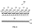
- metal contacts 112 and 113 are formed in the contact holes to make electrical connection to corresponding diffusion regions.
- the metal contacts 112 are formed in contact holes to make electrical connection to the P-type diffusion regions.
- the metal contacts 113 are formed in contact holes to make electrical connection to the N-type diffusion regions.
- the metal contacts 112 and 113 may be interdigitated, and may comprise copper or other single layer or multi-layer electrically conductive materials employed for metallization.
- the metal contacts 112 and 113 may be formed by electro-plating, for example.
- the metal contacts 112 and 113 allow an electrical circuit to be coupled to and be powered by the solar cell.
- a metal contact 112 to a P-type diffusion region may pass over an N-type diffusion region.
- a metal contact 113 to an N-type diffusion region may pass over a P-type diffusion region. Because the metal contacts are formed in contact holes formed by laser ablation, the chances of a metal contact electrically shorting to an opposite polarity diffusion region is greatly diminished.
- FIG. 7 shows another top view of a portion of the solar cell 300 of FIG. 1 .
- the solar cell 300 includes contact holes 307 that are formed through an interlayer dielectric separating the P-polarity metal contact 303 from underlying diffusion regions.
- FIG. 8 shows a cross-section of the solar cell 300 taken at section B-B of FIG. 7 .
- Contact holes 307 i.e., 307-1, 307-2,...) are formed through the interlayer dielectric 305 to allow the P-polarity metal contact 303 to electrically connect to the underlying P-type diffusion region.
- the contact holes 307 are formed by laser ablation. If the laser is not properly controlled, the laser beam may punch through the diffusion region, thereby adversely affecting the operation of the solar cell by electrically shorting the subsequently formed metal contact to the substrate.
- the laser ablation step formed the contact hole 307-1 all the way through the interlayer dielectric 305, all the way through the P-type diffusion region, and into the substrate 401.
- One way of addressing this laser punch through problem is to make the diffusion regions deeper, as now explained with reference to FIG. 9 .
- FIG. 9 shows a cross-section of a solar cell 400 with deep diffusions in accordance with an embodiment of the present invention.
- a P-type diffusion region (labeled as 402) is formed in a solar cell substrate 411, which comprises a monocrystalline silicon wafer.
- the P-type diffusion region is formed in another layer (e.g., polysilicon) formed on the backside surface of the substrate 411.
- contact holes 405 i.e., 405-1, 405-2,...) are formed through an interlayer dielectric 403 by laser ablation.
- a P-polarity metal contact 404 electrically connects to the P-type diffusion region through the contact holes 405. It is to be noted that all figures in this disclosure, including FIG. 9 , are not drawn to scale.
- the P-type diffusion region is formed to be relatively deep.
- the P-type diffusion region may have a depth 407 deeper than 0.5 ⁇ m.
- the depth of the P-type diffusion region is dictated by the process margins of the laser ablation step.
- the required laser ablation depth is minimized for the process, and then measured on a cross-section.
- the dopant depth of the diffusion region is then set deeper than the required laser ablation depth by controlling the dopant formation process (e.g., furnace temperature and time, starting dopant concentration, etc).
- Deep diffusion regions advantageously allow for a laser ablation step with wider process margins. Deep N-type diffusion regions formed on the backside of the solar cell with the P-type diffusions region may also have the same depth as the P-type diffusion regions.
- the contact hole 405-1 is formed relatively deep into the P-type diffusion region.
- the deep contact hole 405-1 may be due to problems related to process control in general, laser ablation process margin, or other issues.
- the contact hole 405-1 does not punch all the way through the P-type diffusion region because of the depth of the P-type diffusion region.
- the metal contact 404 is formed in the contact holes 405 (i.e., 405-1, 405-2,).
- the metal contact 404 may safely pass over a diffusion region of opposite polarity (i.e., N-type diffusion region) because the metal contact 404 is formed in contact holes formed by laser ablation.
- FIG. 10 An example of such solar cell design is shown in FIG. 10 .
- FIG. 10 shows a cross-section of a solar cell 420 having a non-uniform film 423 through which contact holes are to be formed.
- the film 423 comprises an interlayer dielectric.
- the film 423 may be a single layer dielectric or a multi-layer dielectric stack (e.g., oxides and/or nitrides; oxides and/or polyimide) formed over a solar cell substrate 421.
- the solar cell substrate 421 may comprise a monocrystalline silicon wafer.
- the P-type and N-type diffusion regions may be formed in the solar cell substrate 421 or in another layer (e.g., polysilicon) formed on the solar cell substrate 421.
- portions of the film 423 over the P-type diffusion regions are thicker than portions of the film 423 over the N-type diffusion regions.
- portions of the film 423 over the N-type diffusion regions are thicker than portions of the film 423 over the P-type diffusion regions. This difference in film thicknesses may be due to the process of forming the P-type and N-type diffusion regions, such as in the sequence of forming dopant sources over the diffusion regions. Forming contact holes through the film 423 to the N-type diffusion regions requires less laser energy compared to forming contact holes through the film 423 to the P-type diffusion regions.
- Using the same laser energy to form contact holes to the P-type and N-type diffusion regions may thus result in punching through the P-type diffusion regions, or other problems.
- using different laser energies to form contact holes to the P-type and N-type diffusion regions may require multiple laser ablation steps and may result in processing delays not just because of the additional steps, but also in reconfiguring the laser for different energies.
- the thickness of the dielectric stack over the P-type diffusion regions may be in the 500-10000 Angstroms range, and the diffusion depth of the P-type diffusion regions may be in the 200-2000 nm range.
- the standard bulk recombination rate (BRR) and saturation current density ( Jo ) would be less than 1000Hz and 120 fA/cm 2 if there were no laser damage.
- BRR bulk recombination rate
- Jo saturation current density
- the laser ablation tool gets relatively complicated, requiring changes in power for different regions of the solar cell being fabricated.
- the dielectric stack may be tuned so that the ideal laser parameter, such as energy and number of pulses, on one region does not result in ablation in another region.
- dielectric stack thickness over the P-type diffusion regions may be made to be 5000-10000 Angstroms
- the dielectric stack thickness over the N-type diffusion regions may be made to be less than 2500 Angstroms. This allows a laser energy of 3 ⁇ J with two pulses to ablate the dielectric stack over the N-type diffusion regions, but not the dielectric stack over the P-type diffusion regions.
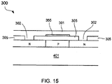
- FIG. 15 shows the cross-section of FIG. 3 except for the addition of an additional dielectric layer 355 patterned on portions of the interlayer dielectric layer 305 over the P-type diffusion regions. Other components shown in FIG. 15 have been discussed with reference to FIG. 3 .
- the additional dielectric layer 355 may comprise a material that may be ablated sacrificially, such as a pigmented ink.
- the additional dielectric layer 355 may be thick enough (e.g., greater than 500 Angstroms) to prevent absorption of the laser wavelength used.
- the additional dielectric layer 355 may also comprise a material that is transparent to the laser (e.g., polyimide) but thick enough (e.g., greater than 500 Angstroms) to prevent the ablated material underneath from breaking through.
- the additional dielectric layer 355 may also comprise a semi-transparent material, provided that the combination of direct ablation of the sacrificial layer and ejected material from below does not cause a pinhole to form in the additional dielectric layer 355. It should be noted that this additional dielectric layer 355 may also have properties that prevent dielectric breakdown, as discussed later below.
- the solar cell 420 of FIG. 10 is prepared for laser ablation by removing the film 423 and any other material previously formed on the P-type and N-type diffusion regions.
- This approach is especially advantageous in cases where the dielectric stacks vary from each other by more than 200 Angstroms.
- FIG. 11 where all materials on the P-type and N-type diffusion regions have been removed to expose the backside surface of the P-type and N-type diffusion regions.
- the film 423 of FIG. 10 may be removed using a conventional wet etch process. The film 423 and any other material on the P-type and N-type diffusion regions are removed to control the thickness of the film subsequently formed on the P-type and N-type diffusion regions.
- a substantially uniform film 424 is formed on the P-type and N-type diffusion regions.
- the film 424 replaces the non-uniform film 423.
- the film 424 may comprise an interlayer dielectric (e.g., deposited or thermally grown oxide, followed by silicon nitride) that is deposited with substantially uniform thickness.
- the film 424 may be deposited by chemical vapor deposition, other deposition, or growth process that allows for uniform film deposition.
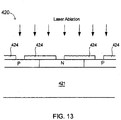
- the replacement of the non-uniform film 423 with the uniform film 424 is subsequently followed by a laser ablation step to form contact holes through the film 424 to expose portions of the P-type and N-type diffusion regions.
- the contact holes allow metal contacts to electrically connect to corresponding diffusion regions.
- a metal contact to a P-type diffusion region may pass over an N-type diffusion region.
- a metal contact to an N-type diffusion region may pass over a P-type diffusion region. Because the metal contacts are formed in contact holes formed by laser ablation, the chances of a metal contact electrically shorting to an opposite polarity diffusion region is greatly diminished.
- Contact holes through the film 423 of FIG. 10 may also be formed by appropriate control of the laser used in the laser ablation step.
- Typical ablation of dielectric films is through the process of indirect ablation, where the laser energy is absorbed in the substrate, and the film is ejected via the outward force of the ablated substrate.
- This type of film ablation is known as indirect ablation.
- ablation depth and damage in the substrate are driven primarily by pulse length, wavelength, and number of pulses of the laser, all of which need to be reduced for minimal substrate ablation depth.
- the laser process parameters will need to be adjusted accordingly, for example, by increasing the number of pulses or by switching the laser wavelength so that direct ablation occurs.
- Certain types of films may be removed via direct ablation, without ablation in the silicon, by using multiple pulses.
- An example laser ablation process using multiple laser pulses is described in commonly-owned U.S. Application No. 12/795,526, filed on June 7, 2010 , and incorporated herein by reference in its entirety.
- Other multi-pulse laser ablation processes may also be used without detracting from the merits of the present invention.
- a method to modify the optical properties of a dielectric layer (e.g., P-type or N-type doped silicon dioxide) or dielectric stack to suit laser ablation parameters may include tuning refractive index and absorption coefficients of the dielectric through compositional control, or by adding absorbing compounds to the dielectric layer to tune the dielectric layer to get either direct or indirect ablation.
- refractive indices less than 2.0 for laser wavelengths of 530 nm or longer cause indirect ablation to occur and prevent residual material from remaining on the substrate.
- a first laser ablation step may be performed to form contact holes through portions of the film 423 over the P-type diffusion regions.
- the first laser ablation step may be in accordance with a first laser configuration having parameters tailored specifically for the characteristics of the portions of the film 423 over the P-type diffusion regions.
- a second laser ablation step may be performed to form contact holes through portions of the film 423 over the N-type diffusion regions.
- the second laser ablation step may be in accordance with a second laser configuration having parameters tailored specifically for the characteristics of the portions of the film 423 over the N-type diffusion regions.
- the first configuration being different from the second configuration.
- the first configuration may involve the laser firing multiple laser pulses to drill through portions of the film 423 over the P-type diffusion regions.
- the second configuration may involve the laser firing a single laser pulse to drill through portions of the film 423 over the N-type diffusion regions.
- the resulting structure is schematically shown in FIG. 14 , where the contact holes 435-1 and 435-2 through the film 423 and exposing the P-type diffusion regions are formed by laser ablation with the laser firing in accordance with the first configuration, and the contact hole 435-3 through the film 423 and exposing an N-type diffusion region is formed by laser ablation with the laser firing in accordance with the second configuration.
- Metal contacts may be formed in the contact holes 435 (i.e., 435-1, 435-2, 435-3).
- a metal contact may be safely formed over a diffusion region of opposite polarity (e.g., N-polarity metal contact over a P-type diffusion region) because the metal contacts are in contact holes formed by laser ablation.
- the anti-reflective coating deposited on the backside may be tailored in a way to improve the dielectric integrity of the back stack.
- the thickness and/or resistivity of the backside anti-reflective coating may be increased by approximately 50-100 Angstroms.
- the anti-reflective coating may comprise two layers, such as a layer of amorphous-silicon that is uniformly deposited on top or underneath a silicon nitride layer.
- the layer of amorphous silicon and the silicon nitride layer are formed in-situ (i.e., same loading) in the same process step in the same tool.
- the use of a two layer anti-reflective coating as described herein advantageously increases not just the thickness of the anti-reflective coating but also its dielectric constant, thereby facilitating laser ablation.
- a target breakdown field of the dielectric film for such an application can be greater than 1x10 7 V/cm.
- the target breakdown field may be achieved by addition of 50-100 Angstrom layer of amorphous silicon to the silicon nitride layer, which could decrease the effective field applied within the stack.
Landscapes
- Photovoltaic Devices (AREA)
- Life Sciences & Earth Sciences (AREA)
- Sustainable Development (AREA)
- Engineering & Computer Science (AREA)
- Sustainable Energy (AREA)
- Laser Beam Processing (AREA)
Abstract
Description
- The invention described herein was made with Governmental support under contract number DE-FC36-07GO17043 awarded by the United States Department of Energy. The Government may have certain rights in the invention.
- Embodiments of the subject matter described herein relate generally to solar cells. More particularly, embodiments of the subject matter relate to solar cell fabrication processes and structures.
- Solar cells are well known devices for converting solar radiation to electrical energy. They may be fabricated on a semiconductor wafer using semiconductor processing technology. A solar cell includes P-type and N-type diffusion regions. Solar radiation impinging on the solar cell creates electrons and holes that migrate to the diffusion regions, thereby creating voltage differentials between the diffusion regions. In a back contact, back junction (BCBJ) solar cell, the P-type and N-type diffusion regions and the metal contacts coupled to them are on the backside of the solar cell. The metal contacts allow an external electrical circuit to be coupled to and be powered by the solar cell.
- In high-efficiency solar cells, cell parameters, such as shunt resistance, series resistance, and bulk lifetime are important parameters to maintain on the final fabricated devices. Solar cell process steps, in particular laser ablation steps on BCBJ solar cells, may impact each of these parameters. Post laser losses due to series resistance or lifetime maybe be offset at the expense of step cost, such as by adding thermal or etching steps. As is described within, an added complication of shunting on high-efficiency BCBJ solar cells may be prevalent when the cell architecture has metal of one polarity over diffusions of another polarity.
- To compete with other energy sources available on the market, solar cells not only have to be efficient but also fabricated at relatively low cost and high yield. Embodiments of the present invention pertain to novel solar cell fabrication processes and structures that reduce the cost of solar cell fabrication and improve solar cell reliability.
- In one embodiment, contact holes of solar cells are formed by laser ablation to accommodate various solar cell designs. Use of a laser to form the contact holes is facilitated by replacing films formed on the diffusion regions with a film that has substantially uniform thickness. The film thickness as absorption may be tailored to match laser parameters. Dopant depth underneath contact holes may be controlled to increase the laser ablation process margins. The laser configuration may be tailored to form contact holes through dielectric films of varying thicknesses.
- These and other features of the present invention will be readily apparent to persons of ordinary skill in the art upon reading the entirety of this disclosure, which includes the accompanying drawings and claims.
- A more complete understanding of the subject matter disclosed herein may be derived by referring to the detailed description and claims when considered in conjunction with the following figures, wherein like reference numbers refer to similar elements throughout the figures. The figures are not drawn to scale.
-
FIG. 1 schematically shows an example BCBJ solar cell with metal contacts that are formed over opposite polarity diffusion regions. -
FIG. 2 shows a top view of the solar cell ofFIG. 1 . -
FIG. 3 shows a cross-section of the solar cell ofFIG. 1 taken at section A-A ofFIG. 2 . -
FIGS. 4-6 show cross-sections of a solar cell being fabricated in accordance with an embodiment of the present invention. -
FIG. 7 shows another top view of the solar cell ofFIG. 1 . -
FIG. 8 shows a cross-section of the solar cell ofFIG. 1 taken at section B-B ofFIG. 7 . -
FIG. 9 shows a cross-section of a solar cell with deep diffusion regions in accordance with an embodiment of the present invention. -
FIGS. 10-13 show cross-sections of a solar cell being fabricated in accordance with another embodiment of the present invention. -
FIG. 14 shows a cross-section of a solar cell with laser-formed contact holes in accordance with another embodiment of the present invention. -
FIG. 15 shows the cross-section ofFIG. 3 with an additional dielectric layer in accordance with an embodiment of the present invention. - In the present disclosure, numerous specific details are provided, such as examples of apparatus, processes, and structures, to provide a thorough understanding of embodiments of the invention. Persons of ordinary skill in the art will recognize, however, that the invention can be practiced without one or more of the specific details. In other instances, well-known details are not shown or described to avoid obscuring aspects of the invention.
- In some high-efficiency solar cell designs, metal contacts for one polarity of diffusion region may run over an opposite polarity diffusion region (e.g., metal contact for an N-type diffusion region formed over a P-type diffusion region). In that solar cell design, it is critical that the interlayer dielectric that electrically insulates the metal contacts from the diffusion regions is free of defects. Otherwise, a metal contact of one polarity may electrically short to a diffusion region of opposite polarity through a defect in the interlayer dielectric.
-
FIG. 1 schematically shows an example backside contact, backside junction (BCBJ)solar cell 300 with metal contacts that are formed over opposite polarity diffusion regions. In the example ofFIG. 1 , the P-type (labeled 352) and N-type (labeled 351) diffusion regions are formed in a substrate 401 (e.g., mono-crystalline or multi-crystalline silicon). In other embodiments, the P-type and N-type diffusion regions are formed in another layer, e.g., polysilicon, on a backside surface of the substrate of 401. Interlayer dielectrics are not shown inFIG. 1 for clarity of illustration. - The
solar cell 300 includesmetal contacts Metal contacts 301 are N-polarity metal contacts in that they electrically couple to corresponding N-type diffusion regions. Similarly, metal contacts 303 (only one is shown inFIG. 1 ) are P-polarity metal contacts that electrically couple to corresponding P-type diffusion regions. Themetal contacts metal contact 301 is depicted inFIG. 1 as a transparent line tracing to more clearly show underlying N-type diffusion regions. As shown inFIG. 1 , an N-polarity metal contact 301 passes over portions of a P-type diffusion region. This creates the possibility of the N-polarity metal contact 301 being electrically shorted to the P-type diffusion region through an intervening interlayer dielectric (not shown inFIG. 1 ; see 305 inFIGS. 3 and8 ). -
FIG. 2 shows a top view of a portion of thesolar cell 300. Thesolar cell 300 includescontact holes 302 that are formed through an interlayer dielectric separating the N-polarity metal contact 301 from underlying diffusion regions. The N-polarity metal contact 301 contacts underlying N-type diffusion regions throughcorresponding contact holes 302. -
FIG. 3 shows a cross-section of thesolar cell 300 taken at section A-A ofFIG. 2 . As shown inFIG. 3 , thesolar cell 300 includes an interlayer dielectric 305, which electrically insulates the N-polarity metal contact 301 from underlying diffusion regions.Contact holes 302 are formed through the interlayer dielectric 305 to allow the N-polarity metal contact 301 to electrically connect to corresponding N-type diffusion regions. Thecontact holes 302 are typically formed by conventional masking and wet etching. The inventors discovered that some etchants used in the etch process may worsen existing imperfections (e.g., pinholes, pits, and other defects) in the interlayer dielectric 305, turning the imperfections into full-blown defects. For example, some etchants may enlarge existing pinholes. As another example, some etchants may result in creation of an electrical short 306 through theinterlayer dialect 305. - Using a laser, rather than a conventional wet etch process, to form the contact holes 302 advantageously avoids worsening imperfections that may be present in the
interlayer dielectric 305. By avoiding exposure of theinterlayer dielectric 305 to harmful etchants during contact hole formation, a laser ablation step preserves the integrity of theinterlayer dielectric 305. -
FIG. 4 shows a cross-section of asolar cell 300 being fabricated in accordance with an embodiment of the present invention. Thesolar cell 300 has afront side 153 and abackside 152. Thefront side 153 faces the sun to collect solar radiation during normal operation. Thebackside 152 is opposite thefront side 153. - In the example of
FIG. 4 , thesubstrate 101 comprises an N-type monocrystalline silicon wafer. The P-type and N-type diffusion regions are formed in thesolar cell substrate 101, but may also be in another layer (e.g., polysilicon) formed on thesolar cell substrate 101. The front side surface of thesubstrate 101 is textured with random pyramids to increase solar radiation collection efficiency. Apassivation region 107 passivates the front side surface of thesubstrate 101 to minimize recombination. In one embodiment, thepassivation region 107 is an N-type passivation region formed by diffusing N-type dopants from thefront side 153. The N-type dopants may comprise phosphorus. In one embodiment, thepassivation region 107 is formed by heating thesubstrate 101 in a furnace where phosphorus is introduced. The phosphorus diffuses into the front side of thesubstrate 101 to form thepassivation region 107. Asilicon dioxide layer 108 on theback side 152 of the solar cell is a byproduct of forming thepassivation region 107. More specifically, the heating step to diffuse N-type dopants into thesubstrate 101 and form thepassivation region 107 also results in growth of theoxide layer 108 on the backside surface of thesubstrate 101. - An
anti-reflective coating 109 is formed on thefront side 153 and ananti-reflective coating 110 is formed on thebackside 152. In one embodiment, theanti-reflective coatings front side 153, theanti-reflective coating 109 is formed on thepassivation region 107 on the front side surface of thesubstrate 101. On thebackside 152, theanti-reflective coating 110 is formed on theoxide layer 108. - In
FIG. 5 , a laser ablation step is performed on thesolar cell 300 to form contact holes to the P-type and N-type diffusion regions. The laser ablation step may involve firing one or more laser beams to remove materials from thebackside 152 and thereby expose the P-type and N-type diffusion regions for metallization. In the example ofFIG. 5 , the laser ablation step removes portions of theanti-reflective coating 110 andoxide layer 108 to form contact holes to the P-type and N-type diffusion regions. The laser ablation step may be performed by firing laser beams through a laser scanner, which scans the laser beams on thebackside 152 to form the contact holes. A commercially available laser source and scanner may be employed to perform the laser ablation. An example solar cell ablation system that employs a laser is disclosed in commonly-ownedU.S. Application No. 12/829,275, filed on July 1, 2010 - The use of a laser to form the contact holes to the P-type and N-type diffusion regions advantageously eliminates masking and curing steps that may be necessary in other processes where the contact holes are formed by a traditional etch process. In addition, laser ablation prevents exposure of the
anti-reflective coating 110 andoxide layer 108, and any interlayer dielectric that may be present, to etchants that may worsen existing defects or imperfections. - In
FIG. 6 ,metal contacts FIG. 6 , themetal contacts 112 are formed in contact holes to make electrical connection to the P-type diffusion regions. Similarly, themetal contacts 113 are formed in contact holes to make electrical connection to the N-type diffusion regions. Themetal contacts metal contacts metal contacts metal contact 112 to a P-type diffusion region may pass over an N-type diffusion region. Similarly, ametal contact 113 to an N-type diffusion region may pass over a P-type diffusion region. Because the metal contacts are formed in contact holes formed by laser ablation, the chances of a metal contact electrically shorting to an opposite polarity diffusion region is greatly diminished. - A potential laser-related problem discovered by the inventors is now described with reference to
FIGS. 7 and 8. FIG. 7 shows another top view of a portion of thesolar cell 300 ofFIG. 1 . Thesolar cell 300 includes contact holes 307 that are formed through an interlayer dielectric separating the P-polarity metal contact 303 from underlying diffusion regions. -
FIG. 8 shows a cross-section of thesolar cell 300 taken at section B-B ofFIG. 7 . Contact holes 307 (i.e., 307-1, 307-2,...) are formed through theinterlayer dielectric 305 to allow the P-polarity metal contact 303 to electrically connect to the underlying P-type diffusion region. - In the example of
FIG. 8 , the contact holes 307 are formed by laser ablation. If the laser is not properly controlled, the laser beam may punch through the diffusion region, thereby adversely affecting the operation of the solar cell by electrically shorting the subsequently formed metal contact to the substrate. In the example ofFIG. 8 , the laser ablation step formed the contact hole 307-1 all the way through theinterlayer dielectric 305, all the way through the P-type diffusion region, and into thesubstrate 401. One way of addressing this laser punch through problem is to make the diffusion regions deeper, as now explained with reference toFIG. 9 . -
FIG. 9 shows a cross-section of asolar cell 400 with deep diffusions in accordance with an embodiment of the present invention. In the example ofFIG. 9 , a P-type diffusion region (labeled as 402) is formed in asolar cell substrate 411, which comprises a monocrystalline silicon wafer. In other embodiments, the P-type diffusion region is formed in another layer (e.g., polysilicon) formed on the backside surface of thesubstrate 411. In the example ofFIG. 9 , contact holes 405 (i.e., 405-1, 405-2,...) are formed through aninterlayer dielectric 403 by laser ablation. A P-polarity metal contact 404 electrically connects to the P-type diffusion region through the contact holes 405. It is to be noted that all figures in this disclosure, includingFIG. 9 , are not drawn to scale. - In the example of
FIG. 9 , the P-type diffusion region is formed to be relatively deep. For example, the P-type diffusion region may have adepth 407 deeper than 0.5 µm. The depth of the P-type diffusion region is dictated by the process margins of the laser ablation step. Preferably, the required laser ablation depth is minimized for the process, and then measured on a cross-section. The dopant depth of the diffusion region is then set deeper than the required laser ablation depth by controlling the dopant formation process (e.g., furnace temperature and time, starting dopant concentration, etc). Deep diffusion regions advantageously allow for a laser ablation step with wider process margins. Deep N-type diffusion regions formed on the backside of the solar cell with the P-type diffusions region may also have the same depth as the P-type diffusion regions. - In the example of
FIG. 9 , the contact hole 405-1 is formed relatively deep into the P-type diffusion region. The deep contact hole 405-1 may be due to problems related to process control in general, laser ablation process margin, or other issues. However, unlike inFIG. 8 , the contact hole 405-1 does not punch all the way through the P-type diffusion region because of the depth of the P-type diffusion region. Themetal contact 404 is formed in the contact holes 405 (i.e., 405-1, 405-2,...). Themetal contact 404 may safely pass over a diffusion region of opposite polarity (i.e., N-type diffusion region) because themetal contact 404 is formed in contact holes formed by laser ablation. - The inventors also discovered that different film thicknesses found in some solar cell designs may complicate laser ablation. An example of such solar cell design is shown in
FIG. 10 . -
FIG. 10 shows a cross-section of asolar cell 420 having anon-uniform film 423 through which contact holes are to be formed. In the example ofFIG. 10 , thefilm 423 comprises an interlayer dielectric. Thefilm 423 may be a single layer dielectric or a multi-layer dielectric stack (e.g., oxides and/or nitrides; oxides and/or polyimide) formed over asolar cell substrate 421. Thesolar cell substrate 421 may comprise a monocrystalline silicon wafer. The P-type and N-type diffusion regions may be formed in thesolar cell substrate 421 or in another layer (e.g., polysilicon) formed on thesolar cell substrate 421. - In the example of
FIG. 10 , portions of thefilm 423 over the P-type diffusion regions are thicker than portions of thefilm 423 over the N-type diffusion regions. In other cases, portions of thefilm 423 over the N-type diffusion regions are thicker than portions of thefilm 423 over the P-type diffusion regions. This difference in film thicknesses may be due to the process of forming the P-type and N-type diffusion regions, such as in the sequence of forming dopant sources over the diffusion regions. Forming contact holes through thefilm 423 to the N-type diffusion regions requires less laser energy compared to forming contact holes through thefilm 423 to the P-type diffusion regions. Using the same laser energy to form contact holes to the P-type and N-type diffusion regions may thus result in punching through the P-type diffusion regions, or other problems. On the other hand, using different laser energies to form contact holes to the P-type and N-type diffusion regions may require multiple laser ablation steps and may result in processing delays not just because of the additional steps, but also in reconfiguring the laser for different energies. - For the solar cell design of
FIG. 10 , the thickness of the dielectric stack over the P-type diffusion regions may be in the 500-10000 Angstroms range, and the diffusion depth of the P-type diffusion regions may be in the 200-2000 nm range. For a high-efficiency solar cell, i.e., a solar cell with efficiency greater than 20%, the standard bulk recombination rate (BRR) and saturation current density (Jo) would be less than 1000Hz and 120 fA/cm2 if there were no laser damage. To avoid ablation all the way through the junction in the base and increase the BRR and Jo, while also completely removing the film being ablated, the proper laser condition must be used. Using a wavelength shorter than 540nm while keeping the absorption depth to a minimum prevents the BRR from increasing higher than 1000Hz. Using a laser with a pulse length shorter than 20ps will keep the thermal ablation depth to less than 2000nm. The laser energy would then be tuned so that the ablation threshold is achieved (e.g., 1-20µJ). Complete oxide removal would then result in series resistance of less than 1 ohm-cm2 in the finished solar cell. However, with these film stack thickness conditions on a high-efficiency solar cell, a single laser pulse will still not be able to clear an entire dielectric stack without increasing the BRR and Jo. That is, keeping the BRR to less than 1000Hz and Jo to less than 120fA/cm2 will result in series resistance greater than 1 ohm-cm2, and getting the series resistance less than 1ohm-cm2 will result in the BRR increasing higher than 1000Hz. This problem may be solved by using 2 or more laser pulses, where the pulse to pulse spacing is separated by less than 500ns and the amplitude of the subsequent pulses is between 10% and 100% the amplitude of the first pulse. This allows for more material removal without additional increase in BRR and Jo. An example multi-pulse laser ablation process is described in commonly-owned U.S. Application No. 12/795,526, filed on June 7, 2010, and incorporated herein by reference in its entirety. Other multi-pulse laser ablation processes may also be used. - Because the dielectric stack thicknesses over the P-type and N-type diffusion regions may be different, and thus require different laser energies to achieve the proper BRR / series resistance balance, the laser ablation tool gets relatively complicated, requiring changes in power for different regions of the solar cell being fabricated. This requires precise spatial coordination between the laser and the beam delivery system to synchronize laser power and location and avoid creating shunts (i.e., electrical shorts) due to a misaligned laser. Misalignment can be avoided by slowing down the beam delivery system. However, doing so would result in lower throughput on the tool, and therefore increase the tool cost for a certain throughput. As a solution, the dielectric stack may be tuned so that the ideal laser parameter, such as energy and number of pulses, on one region does not result in ablation in another region. For example, dielectric stack thickness over the P-type diffusion regions may be made to be 5000-10000 Angstroms, and the dielectric stack thickness over the N-type diffusion regions may be made to be less than 2500 Angstroms. This allows a laser energy of 3 µJ with two pulses to ablate the dielectric stack over the N-type diffusion regions, but not the dielectric stack over the P-type diffusion regions.
- In any case where laser misalignment may cause a shunt problem as described above (e.g., in
FIG. 3 , the electrical short 306), the inventors have discovered that an additional dielectric layer may be deposited in a patterned way so that the laser is blocked from causing ablation.FIG. 15 shows the cross-section ofFIG. 3 except for the addition of an additionaldielectric layer 355 patterned on portions of theinterlayer dielectric layer 305 over the P-type diffusion regions. Other components shown inFIG. 15 have been discussed with reference toFIG. 3 . - In the example of
FIG. 15 , the additionaldielectric layer 355 may comprise a material that may be ablated sacrificially, such as a pigmented ink. The additionaldielectric layer 355 may be thick enough (e.g., greater than 500 Angstroms) to prevent absorption of the laser wavelength used. The additionaldielectric layer 355 may also comprise a material that is transparent to the laser (e.g., polyimide) but thick enough (e.g., greater than 500 Angstroms) to prevent the ablated material underneath from breaking through. The additionaldielectric layer 355 may also comprise a semi-transparent material, provided that the combination of direct ablation of the sacrificial layer and ejected material from below does not cause a pinhole to form in the additionaldielectric layer 355. It should be noted that this additionaldielectric layer 355 may also have properties that prevent dielectric breakdown, as discussed later below. - In accordance with an embodiment of the present invention, the
solar cell 420 ofFIG. 10 is prepared for laser ablation by removing thefilm 423 and any other material previously formed on the P-type and N-type diffusion regions. This approach is especially advantageous in cases where the dielectric stacks vary from each other by more than 200 Angstroms. This approach is further illustrated inFIG. 11 where all materials on the P-type and N-type diffusion regions have been removed to expose the backside surface of the P-type and N-type diffusion regions. For example, thefilm 423 ofFIG. 10 may be removed using a conventional wet etch process. Thefilm 423 and any other material on the P-type and N-type diffusion regions are removed to control the thickness of the film subsequently formed on the P-type and N-type diffusion regions. Accordingly, in the example ofFIG. 12 , a substantiallyuniform film 424 is formed on the P-type and N-type diffusion regions. In essence, thefilm 424 replaces thenon-uniform film 423. Thefilm 424 may comprise an interlayer dielectric (e.g., deposited or thermally grown oxide, followed by silicon nitride) that is deposited with substantially uniform thickness. Thefilm 424 may be deposited by chemical vapor deposition, other deposition, or growth process that allows for uniform film deposition. InFIG. 13 , the replacement of thenon-uniform film 423 with theuniform film 424 is subsequently followed by a laser ablation step to form contact holes through thefilm 424 to expose portions of the P-type and N-type diffusion regions. The contact holes allow metal contacts to electrically connect to corresponding diffusion regions. A metal contact to a P-type diffusion region may pass over an N-type diffusion region. Similarly, a metal contact to an N-type diffusion region may pass over a P-type diffusion region. Because the metal contacts are formed in contact holes formed by laser ablation, the chances of a metal contact electrically shorting to an opposite polarity diffusion region is greatly diminished. - Contact holes through the
film 423 ofFIG. 10 may also be formed by appropriate control of the laser used in the laser ablation step. Typical ablation of dielectric films is through the process of indirect ablation, where the laser energy is absorbed in the substrate, and the film is ejected via the outward force of the ablated substrate. This type of film ablation is known as indirect ablation. For example, when the film of interest does not interact strongly with the laser wavelength, ablation depth and damage in the substrate are driven primarily by pulse length, wavelength, and number of pulses of the laser, all of which need to be reduced for minimal substrate ablation depth. If the film or one of the films in a film stack of interest interacts strongly with the laser wavelength, the laser process parameters will need to be adjusted accordingly, for example, by increasing the number of pulses or by switching the laser wavelength so that direct ablation occurs. Certain types of films may be removed via direct ablation, without ablation in the silicon, by using multiple pulses. An example laser ablation process using multiple laser pulses is described in commonly-ownedU.S. Application No. 12/795,526, filed on June 7, 2010 - A method to modify the optical properties of a dielectric layer (e.g., P-type or N-type doped silicon dioxide) or dielectric stack to suit laser ablation parameters may include tuning refractive index and absorption coefficients of the dielectric through compositional control, or by adding absorbing compounds to the dielectric layer to tune the dielectric layer to get either direct or indirect ablation. As a particular example, refractive indices less than 2.0 for laser wavelengths of 530 nm or longer cause indirect ablation to occur and prevent residual material from remaining on the substrate.
- As applied to
FIG. 10 , a first laser ablation step may be performed to form contact holes through portions of thefilm 423 over the P-type diffusion regions. The first laser ablation step may be in accordance with a first laser configuration having parameters tailored specifically for the characteristics of the portions of thefilm 423 over the P-type diffusion regions. A second laser ablation step may be performed to form contact holes through portions of thefilm 423 over the N-type diffusion regions. The second laser ablation step may be in accordance with a second laser configuration having parameters tailored specifically for the characteristics of the portions of thefilm 423 over the N-type diffusion regions. The first configuration being different from the second configuration. For example, the first configuration may involve the laser firing multiple laser pulses to drill through portions of thefilm 423 over the P-type diffusion regions. As another example, the second configuration may involve the laser firing a single laser pulse to drill through portions of thefilm 423 over the N-type diffusion regions. - The resulting structure is schematically shown in
FIG. 14 , where the contact holes 435-1 and 435-2 through thefilm 423 and exposing the P-type diffusion regions are formed by laser ablation with the laser firing in accordance with the first configuration, and the contact hole 435-3 through thefilm 423 and exposing an N-type diffusion region is formed by laser ablation with the laser firing in accordance with the second configuration. Metal contacts may be formed in the contact holes 435 (i.e., 435-1, 435-2, 435-3). A metal contact may be safely formed over a diffusion region of opposite polarity (e.g., N-polarity metal contact over a P-type diffusion region) because the metal contacts are in contact holes formed by laser ablation. - In another embodiment, where defects in an interlayer dielectric, such as the one described with reference to
FIG. 3 , may be present, the anti-reflective coating deposited on the backside (e.g.,anti-reflective coating 110 ofFIGS. 4-6 ) may be tailored in a way to improve the dielectric integrity of the back stack. For example, the thickness and/or resistivity of the backside anti-reflective coating may be increased by approximately 50-100 Angstroms. As another example, the anti-reflective coating may comprise two layers, such as a layer of amorphous-silicon that is uniformly deposited on top or underneath a silicon nitride layer. Preferably, to save fabrication cost, the layer of amorphous silicon and the silicon nitride layer are formed in-situ (i.e., same loading) in the same process step in the same tool. The use of a two layer anti-reflective coating as described herein advantageously increases not just the thickness of the anti-reflective coating but also its dielectric constant, thereby facilitating laser ablation. - In reverse bias, for example, upwards of 6 volts may be applied across the interlayer dielectric film. Typical plasma-enhanced chemical vapor deposition (PECVD) nitride films having a thickness in the range of about 400 Angstroms would breakdown at this voltage if the voltage were applied locally. A target breakdown field of the dielectric film for such an application can be greater than 1x10⁷ V/cm. The target breakdown field may be achieved by addition of 50-100 Angstrom layer of amorphous silicon to the silicon nitride layer, which could decrease the effective field applied within the stack.
- Improved processes and structures for fabricating solar cells have been disclosed. While specific embodiments of the present invention have been provided, it is to be understood that these embodiments are for illustration purposes and not limiting. Many additional embodiments will be apparent to persons of ordinary skill in the art reading this disclosure.
-
- 1. A process of fabricating a solar cell, the process comprising:
- removing materials previously formed on a plurality of P-type and N-type diffusion regions to expose a backside surface of the plurality of P-type and N-type diffusion regions;
- forming a layer of dielectric on the plurality of P-type and N-type diffusion regions;
- using a laser to form a plurality of contact holes through the layer of dielectric, each contact hole in the plurality of contact holes exposing a surface of a corresponding P-type or N-type diffusion region in the plurality of P-type and N-type diffusion regions; and
- forming a metal contact in each of the plurality of contact holes to form an electrical connection to each of the plurality of P-type and N-type diffusion regions.
- 2. The process of item 1 wherein the plurality of P-type and N-type diffusion regions is formed in a solar cell substrate.
- 3. The process of item 2 wherein the solar cell substrate comprises a monocrystalline silicon wafer.
- 4. The process of item 1 wherein the plurality of P-type and N-type diffusion regions is formed in another layer formed on a solar cell substrate.
- 5. The process of item 4 wherein the other layer comprises polysilicon.
- 6. The process of item 1 wherein a metal contact making electrical connection to a P-type diffusion region in the plurality of P-type and N-type diffusion regions passes over an N-type diffusion region in the plurality of P-type and N-type diffusion regions.
- 7. A solar cell fabricated using the process of item 1.
- 8. A process of fabricating a solar cell, the process comprising:
- providing a solar cell structure having a plurality of P-type and N-type diffusion regions;
- using a laser to form a plurality of contact holes through at least one layer of dielectric that is formed on the plurality of P-type and N-type diffusion regions, each contact hole in the plurality of contact holes exposing a surface of a corresponding P-type or N-type diffusion region in the plurality of P-type and N-type diffusion regions; and
- forming a metal contact in each of the plurality of contact holes to form an electrical connection to each of the plurality of P-type and N-type diffusion regions, wherein a metal contact making electrical connection to a P-type diffusion region in the plurality of P-type and N-type diffusion regions passes over an N-type diffusion region in the plurality of P-type and N-type diffusion regions.
- 9. The process of item 8 wherein contact holes to P-type diffusion regions in the plurality of P-type and N-type diffusion regions are formed with the laser firing in accordance with a first configuration, and contact holes to N-type diffusion regions in the plurality of P-type and N-type diffusion regions are formed with the laser firing in accordance with a second configuration that is different from the first configuration.
- 10. The process of item 9 wherein the first configuration involves the laser firing multiple laser pulses to form a contact hole to a P-type diffusion region.
- 11. The process of item 8 wherein the plurality of P-type and N-type diffusion regions is formed in a solar cell substrate.
- 12. The process of item 11 wherein the solar cell substrate comprises a monocrystalline silicon wafer.
- 13. The process of item 8 wherein the plurality of P-type and N-type diffusion regions is formed in another layer formed on a solar cell substrate.
- 14. The process of item 13 wherein the other layer comprises polysilicon.
- 15. A solar cell fabricated using the process of item 8.
- 16. A process of fabricating a solar cell, the process comprising:
- forming a deep diffusion region of a solar cell, the deep diffusion having a depth of at least 0.5 µm;
- using a laser to form a contact hole through a dielectric layer to expose the deep diffusion region; and
- forming a metal contact in the contact hole to electrically connect to the deep diffusion region.
- 17. The process of item 16 wherein the deep diffusion region is P-type and the metal contact passes over an N-type diffusion region.
- 18. The process of item 16 wherein the deep diffusion region is formed in a solar cell substrate that comprises a monocrystalline silicon wafer.
- 19. The process of item 16 wherein the deep diffusion region and another deep diffusion region are formed on a backside of the solar cell, the deep diffusion being a P-type diffusion region and the other deep diffusion region being an N-type diffusion region.
- 20. A solar cell fabricated using the process of item 16.
- 21 A process of fabricating a solar cell, the process comprising:
- forming an anti-reflective coating over an interlayer dielectric on a backside of a solar cell, the anti-reflective coating together with the interlayer dielectric being configured to have a particular breakdown voltage;
- using a laser to form a contact hole through the dielectric layer and the anti-reflective to expose a diffusion region; and
- forming a metal contact in the contact hole to electrically connect to the diffusion region.
- 22. The process of item 21 wherein the anti-reflective coating comprises a layer of amorphous silicon and a layer of silicon nitride.
- 23. The process of item 21 wherein the particular breakdown voltage is greater than 1x10⁷ V/cm.
- 24. The process of item 21 wherein the particular breakdown voltage is configured by decreasing a refractive index of the interlayer dielectric to less than 1.95
- 25. A solar cell fabricated using the process of item 21.
- 26. A process of fabricating a solar cell, the process comprising:
- forming a dielectric stack on a doped substrate, the dielectric stack having an optical property configured for a particular type of laser ablation;
- using a laser to form a contact hole through the dielectric stack by the particular type of laser ablation; and
- forming a metal contact in the contact hole to electrically connect to the doped region.
- 27. The process of item 26 wherein the particular type of laser ablation comprises indirect ablation.
- 28. The process of item 27 wherein the dielectric stack has a refractive index less than 1.97 and the laser has a wavelength equal to or longer than 530 nm.
- 29. The process of item 26 wherein the dielectric comprises doped silicon dioxide.
- 30. A solar cell fabricated using the process of item 26.
Claims (15)
- A solar cell comprising:a P-type diffusion region and a plurality of N-type diffusion regions;a P-type metal contact that is electrically coupled to the P-type diffusion region;an N-type metal contact that is electrically coupled to the N-type diffusion regions and passes over portions of the P-type diffusion region;a first dielectric layer comprising contact holes that allows the N-type metal contact to electrically connect to the N-type diffusion regions, the first dielectric layer is configured to electrically insulate the N-type metal contact from the underlying P-type diffusion region; anda second dielectric layer (355) between the N-type metal contact and the first dielectric layer and over the P-type diffusion regions.
- The solar cell of claim 1, wherein the second dielectric layer (355) comprises pigmented ink.
- The solar cell of claim 1, wherein the second dielectric layer (355) comprises polyimide.
- The solar cell of claim 1, wherein the second dielectric layer (355) has a thickness greater than 500 Angstroms.
- The solar cell of claim 1, wherein the first and second dielectric layers are configured to have a breakdown voltage greater than 1x10⁷ V/cm.
- The solar cell of claim 1, wherein the solar cell is a backside contact solar cell.
- The solar cell of any one of claims 1 to 6, wherein the P-type contact passes over the N-type diffusion region.
- The solar cell of any one of claims 1 to 7, wherein the P-type diffusion region and the N-type diffusion regions are formed in a solar cell substrate.
- The solar cell of claim 8, wherein the solar cell substrate comprises a monocrystalline silicon wafer.
- The solar cell of any one of claims 1 to 7, wherein the P-type diffusion region and the N-type diffusion regions are formed in another layer formed on a solar cell substrate.
- The solar cell of claim 10, wherein the another layer comprises polysilicon.
- The solar cell of claim 1, wherein the second dielectric layer (355) comprises a semi-transparent material.
- The solar cell of claim 1, wherein the first dielectric layer comprises an interlayer dielectric.
- The solar cell of claim 13, wherein the second dielectric layer comprises a sacrificial layer.
- The solar cell of claim 1, wherein portions of the first dielectric layer disposed over the P-type diffusion region are thicker than portions of the first dielectric layer disposed over the N-type diffusion region.
Applications Claiming Priority (3)
| Application Number | Priority Date | Filing Date | Title |
|---|---|---|---|
| US13/028,059 US8586403B2 (en) | 2011-02-15 | 2011-02-15 | Process and structures for fabrication of solar cells with laser ablation steps to form contact holes |
| EP11858937.3A EP2676302B1 (en) | 2011-02-15 | 2011-09-20 | Process and structures for fabrication of solar cells |
| PCT/US2011/052313 WO2012112191A1 (en) | 2011-02-15 | 2011-09-20 | Process and structures for fabrication of solar cells |
Related Parent Applications (1)
| Application Number | Title | Priority Date | Filing Date |
|---|---|---|---|
| EP11858937.3A Division EP2676302B1 (en) | 2011-02-15 | 2011-09-20 | Process and structures for fabrication of solar cells |
Publications (2)
| Publication Number | Publication Date |
|---|---|
| EP3758071A1 true EP3758071A1 (en) | 2020-12-30 |
| EP3758071B1 EP3758071B1 (en) | 2022-04-13 |
Family
ID=46635968
Family Applications (2)
| Application Number | Title | Priority Date | Filing Date |
|---|---|---|---|
| EP20190231.9A Active EP3758071B1 (en) | 2011-02-15 | 2011-09-20 | Structures for fabrication of solar cells |
| EP11858937.3A Active EP2676302B1 (en) | 2011-02-15 | 2011-09-20 | Process and structures for fabrication of solar cells |
Family Applications After (1)
| Application Number | Title | Priority Date | Filing Date |
|---|---|---|---|
| EP11858937.3A Active EP2676302B1 (en) | 2011-02-15 | 2011-09-20 | Process and structures for fabrication of solar cells |
Country Status (9)
| Country | Link |
|---|---|
| US (5) | US8586403B2 (en) |
| EP (2) | EP3758071B1 (en) |
| JP (4) | JP5819990B2 (en) |
| KR (4) | KR102142818B1 (en) |
| CN (3) | CN103370801B (en) |
| AU (1) | AU2011359381B2 (en) |
| SG (3) | SG10201601100RA (en) |
| TW (2) | TWI555219B (en) |
| WO (1) | WO2012112191A1 (en) |
Families Citing this family (24)
| Publication number | Priority date | Publication date | Assignee | Title |
|---|---|---|---|---|
| US8692111B2 (en) * | 2011-08-23 | 2014-04-08 | Sunpower Corporation | High throughput laser ablation processes and structures for forming contact holes in solar cells |
| US20130147003A1 (en) * | 2011-12-13 | 2013-06-13 | Young-Su Kim | Photovoltaic device |
| US10014425B2 (en) * | 2012-09-28 | 2018-07-03 | Sunpower Corporation | Spacer formation in a solar cell using oxygen ion implantation |
| US9812592B2 (en) * | 2012-12-21 | 2017-11-07 | Sunpower Corporation | Metal-foil-assisted fabrication of thin-silicon solar cell |
| US9570576B2 (en) * | 2013-12-10 | 2017-02-14 | Infineon Technologies Ag | Method for forming a semiconductor device having insulating parts or layers formed via anodic oxidation |
| US9218958B2 (en) | 2013-12-10 | 2015-12-22 | Infineon Technologies Ag | Method for forming a semiconductor device |
| KR101620431B1 (en) * | 2014-01-29 | 2016-05-12 | 엘지전자 주식회사 | Solar cell and method for manufacturing the same |
| KR102600379B1 (en) * | 2015-12-21 | 2023-11-10 | 상라오 징코 솔라 테크놀러지 디벨롭먼트 컴퍼니, 리미티드 | Solar cell and method for fabricating therefor |
| US20170236972A1 (en) * | 2016-02-12 | 2017-08-17 | Lg Electronics Inc. | Solar cell and method of manufacturing the same |
| US10217880B2 (en) * | 2016-03-30 | 2019-02-26 | Sunpower Corporation | Voltage breakdown device for solar cells |
| USD822890S1 (en) | 2016-09-07 | 2018-07-10 | Felxtronics Ap, Llc | Lighting apparatus |
| KR101868566B1 (en) * | 2016-11-04 | 2018-06-19 | 엘지전자 주식회사 | Solar cell |
| US10775030B2 (en) | 2017-05-05 | 2020-09-15 | Flex Ltd. | Light fixture device including rotatable light modules |
| USD833061S1 (en) | 2017-08-09 | 2018-11-06 | Flex Ltd. | Lighting module locking endcap |
| USD862777S1 (en) | 2017-08-09 | 2019-10-08 | Flex Ltd. | Lighting module wide distribution lens |
| USD872319S1 (en) | 2017-08-09 | 2020-01-07 | Flex Ltd. | Lighting module LED light board |
| USD877964S1 (en) | 2017-08-09 | 2020-03-10 | Flex Ltd. | Lighting module |
| USD846793S1 (en) | 2017-08-09 | 2019-04-23 | Flex Ltd. | Lighting module locking mechanism |
| USD832494S1 (en) | 2017-08-09 | 2018-10-30 | Flex Ltd. | Lighting module heatsink |
| USD832495S1 (en) | 2017-08-18 | 2018-10-30 | Flex Ltd. | Lighting module locking mechanism |
| USD862778S1 (en) | 2017-08-22 | 2019-10-08 | Flex Ltd | Lighting module lens |
| USD888323S1 (en) | 2017-09-07 | 2020-06-23 | Flex Ltd | Lighting module wire guard |
| CN111584685A (en) * | 2020-05-28 | 2020-08-25 | 江西展宇新能科技有限公司 | A new type of solar cell and its preparation method |
| CN113964212B (en) * | 2021-09-16 | 2022-03-18 | 晶科能源(海宁)有限公司 | A kind of solar cell and its preparation method, photovoltaic module |
Citations (4)
| Publication number | Priority date | Publication date | Assignee | Title |
|---|---|---|---|---|
| US20080017243A1 (en) * | 2006-07-24 | 2008-01-24 | Denis De Ceuster | Solar cell with reduced base diffusion area |
| US20090151784A1 (en) * | 2007-12-14 | 2009-06-18 | Hsin-Chiao Luan | Anti-Reflective Coating With High Optical Absorption Layer For Backside Contact Solar Cells |
| WO2009094575A2 (en) * | 2008-01-24 | 2009-07-30 | Applied Materials, Inc. | Buried insulator isolation for solar cell contacts |
| WO2010033296A1 (en) * | 2008-09-19 | 2010-03-25 | Sunpower Corporation | Method for fabricating a solar cell using a direct-pattern pin-hole-free masking layer |
Family Cites Families (67)
| Publication number | Priority date | Publication date | Assignee | Title |
|---|---|---|---|---|
| US821590A (en) * | 1905-04-13 | 1906-05-22 | Stoddard Haserick Richards & Company | Stop-motion for sliver lap-machines. |
| US4322571A (en) | 1980-07-17 | 1982-03-30 | The Boeing Company | Solar cells and methods for manufacture thereof |
| US4927770A (en) * | 1988-11-14 | 1990-05-22 | Electric Power Research Inst. Corp. Of District Of Columbia | Method of fabricating back surface point contact solar cells |
| US5432015A (en) | 1992-05-08 | 1995-07-11 | Westaim Technologies, Inc. | Electroluminescent laminate with thick film dielectric |
| IL105956A (en) * | 1993-06-08 | 1996-10-16 | Univ Ramot | Laser beam waveguide and laser beam delivery system including same |
| US5738731A (en) | 1993-11-19 | 1998-04-14 | Mega Chips Corporation | Photovoltaic device |
| KR0165423B1 (en) | 1995-07-24 | 1998-12-15 | 김광호 | Connection structure of semiconductor device and manufacturing method thereof |
| JP3467424B2 (en) * | 1998-03-25 | 2003-11-17 | Tdk株式会社 | Solar cell module |
| US6274402B1 (en) * | 1999-12-30 | 2001-08-14 | Sunpower Corporation | Method of fabricating a silicon solar cell |
| US6423568B1 (en) * | 1999-12-30 | 2002-07-23 | Sunpower Corporation | Method of fabricating a silicon solar cell |
| WO2002021602A1 (en) * | 2000-09-08 | 2002-03-14 | Akzo Nobel N.V. | Colored solar cell unit |
| JP2002124692A (en) | 2000-10-13 | 2002-04-26 | Hitachi Ltd | Solar cell and method of manufacturing the same |
| WO2003047005A2 (en) | 2001-11-26 | 2003-06-05 | Shell Solar Gmbh | Manufacturing a solar cell with backside contacts |
| JP4363029B2 (en) | 2002-11-06 | 2009-11-11 | ソニー株式会社 | Manufacturing method of split wave plate filter |
| US7388147B2 (en) * | 2003-04-10 | 2008-06-17 | Sunpower Corporation | Metal contact structure for solar cell and method of manufacture |
| US20060060238A1 (en) | 2004-02-05 | 2006-03-23 | Advent Solar, Inc. | Process and fabrication methods for emitter wrap through back contact solar cells |
| US20050172996A1 (en) | 2004-02-05 | 2005-08-11 | Advent Solar, Inc. | Contact fabrication of emitter wrap-through back contact silicon solar cells |
| DE102004050269A1 (en) * | 2004-10-14 | 2006-04-20 | Institut Für Solarenergieforschung Gmbh | Process for the contact separation of electrically conductive layers on back-contacted solar cells and solar cell |
| US7384714B2 (en) * | 2004-10-25 | 2008-06-10 | Chartered Semiconductor Manufacturing Ltd. | Anti-reflective sidewall coated alternating phase shift mask and fabrication method |
| US20060130891A1 (en) | 2004-10-29 | 2006-06-22 | Carlson David E | Back-contact photovoltaic cells |
| US8129822B2 (en) | 2006-10-09 | 2012-03-06 | Solexel, Inc. | Template for three-dimensional thin-film solar cell manufacturing and methods of use |
| US20090107545A1 (en) | 2006-10-09 | 2009-04-30 | Soltaix, Inc. | Template for pyramidal three-dimensional thin-film solar cell manufacturing and methods of use |
| US8399331B2 (en) | 2007-10-06 | 2013-03-19 | Solexel | Laser processing for high-efficiency thin crystalline silicon solar cell fabrication |
| US8420435B2 (en) | 2009-05-05 | 2013-04-16 | Solexel, Inc. | Ion implantation fabrication process for thin-film crystalline silicon solar cells |
| US20060132028A1 (en) * | 2004-12-16 | 2006-06-22 | Lexmark International, Inc. | Electroluminescent display construction using printing technology |
| US7554031B2 (en) * | 2005-03-03 | 2009-06-30 | Sunpower Corporation | Preventing harmful polarization of solar cells |
| US7279362B2 (en) * | 2005-03-31 | 2007-10-09 | Intel Corporation | Semiconductor wafer coat layers and methods therefor |
| WO2007020833A1 (en) * | 2005-08-12 | 2007-02-22 | Sharp Kabushiki Kaisha | Masking paste, method for producing same, and method for manufacturing solar cell using masking paste |
| CN101278398B (en) * | 2005-09-30 | 2010-09-29 | 株式会社半导体能源研究所 | Method for manufacturing semiconductor device |
| JP5201789B2 (en) * | 2005-11-14 | 2013-06-05 | シャープ株式会社 | Solar cell and method for manufacturing the same |
| US20070169806A1 (en) * | 2006-01-20 | 2007-07-26 | Palo Alto Research Center Incorporated | Solar cell production using non-contact patterning and direct-write metallization |
| KR20080091105A (en) * | 2005-11-24 | 2008-10-09 | 뉴사우스 이노베이션즈 피티와이 리미티드 | High efficiency solar cell manufacturing |
| US20070137692A1 (en) * | 2005-12-16 | 2007-06-21 | Bp Corporation North America Inc. | Back-Contact Photovoltaic Cells |
| WO2007149460A2 (en) | 2006-06-20 | 2007-12-27 | Chism William W | Method of direct coulomb explosion in laser ablation of semiconductor structures |
| DE102006028718B4 (en) | 2006-06-20 | 2008-11-13 | Infineon Technologies Ag | Method for separating semiconductor wafers into semiconductor chips |
| CN1889614B (en) | 2006-07-05 | 2011-07-27 | 珠海格力电器股份有限公司 | Air conditioning system with remote positioning function and controller and control method thereof |
| TWI328877B (en) | 2006-07-20 | 2010-08-11 | Au Optronics Corp | Array substrate |
| FR2906405B1 (en) * | 2006-09-22 | 2008-12-19 | Commissariat Energie Atomique | METHOD OF MAKING DOPED REGIONS IN A SUBSTRATE AND PHOTOVOLTAIC CELL |
| GB2442254A (en) * | 2006-09-29 | 2008-04-02 | Renewable Energy Corp Asa | Back contacted solar cell |
| US7732104B2 (en) | 2007-01-18 | 2010-06-08 | International Business Machines Corporation | System and method for eliminating the structure and edge roughness produced during laser ablation of a material |
| TWI328861B (en) | 2007-03-13 | 2010-08-11 | Au Optronics Corp | Fabrication methods of thin film transistor substrate |
| TW200849627A (en) * | 2007-05-17 | 2008-12-16 | Day4 Energy Inc | Photovoltaic cell with shallow emitter |
| US7838062B2 (en) | 2007-05-29 | 2010-11-23 | Sunpower Corporation | Array of small contacts for solar cell fabrication |
| US20080299279A1 (en) | 2007-06-04 | 2008-12-04 | Land O'lakes, Inc. | Calcium fortification of food powders |
| DE102007059486A1 (en) | 2007-12-11 | 2009-06-18 | Institut Für Solarenergieforschung Gmbh | Rear contact solar cell with elongated, interleaved emitter and base regions at the back and manufacturing method thereof |
| US20090188553A1 (en) | 2008-01-25 | 2009-07-30 | Emat Technology, Llc | Methods of fabricating solar-cell structures and resulting solar-cell structures |
| US7833808B2 (en) | 2008-03-24 | 2010-11-16 | Palo Alto Research Center Incorporated | Methods for forming multiple-layer electrode structures for silicon photovoltaic cells |
| JP2009253096A (en) * | 2008-04-08 | 2009-10-29 | Sharp Corp | Solar battery cell manufacturing method, solar battery module manufacturing method, and solar battery module |
| CN101999175A (en) * | 2008-04-09 | 2011-03-30 | 应用材料股份有限公司 | Simplified back contact for polysilicon emitter solar cells |
| US7851698B2 (en) | 2008-06-12 | 2010-12-14 | Sunpower Corporation | Trench process and structure for backside contact solar cells with polysilicon doped regions |
| US20100013036A1 (en) * | 2008-07-16 | 2010-01-21 | Carey James E | Thin Sacrificial Masking Films for Protecting Semiconductors From Pulsed Laser Process |
| US8258426B2 (en) * | 2008-08-26 | 2012-09-04 | Applied Materials, Inc. | Laser material removal methods and apparatus |
| EP2324509A2 (en) * | 2008-08-27 | 2011-05-25 | Applied Materials, Inc. | Back contact solar cells using printed dielectric barrier |
| US8410568B2 (en) * | 2008-08-29 | 2013-04-02 | Tau-Metrix, Inc. | Integrated photodiode for semiconductor substrates |
| US7999175B2 (en) * | 2008-09-09 | 2011-08-16 | Palo Alto Research Center Incorporated | Interdigitated back contact silicon solar cells with laser ablated grooves |
| JP4937233B2 (en) * | 2008-11-19 | 2012-05-23 | 三菱電機株式会社 | Method for roughening substrate for solar cell and method for manufacturing solar cell |
| US8242354B2 (en) * | 2008-12-04 | 2012-08-14 | Sunpower Corporation | Backside contact solar cell with formed polysilicon doped regions |
| US8283199B2 (en) * | 2009-01-29 | 2012-10-09 | Applied Materials, Inc. | Solar cell patterning and metallization |
| EP2409331A4 (en) * | 2009-03-20 | 2017-06-28 | Intevac, Inc. | Advanced high efficiency crystalline solar cell fabrication method |
| KR101627217B1 (en) * | 2009-03-25 | 2016-06-03 | 엘지전자 주식회사 | Sollar Cell And Fabrication Method Thereof |
| US20120037224A1 (en) * | 2009-04-29 | 2012-02-16 | Mitsubishi Electric Corporation | Solar battery cell and method of manufacturing the same |
| US20100294349A1 (en) * | 2009-05-20 | 2010-11-25 | Uma Srinivasan | Back contact solar cells with effective and efficient designs and corresponding patterning processes |
| KR20120068845A (en) * | 2009-09-20 | 2012-06-27 | 인터몰레큘러 인코퍼레이티드 | Methods of building crystalline silicon solar cells for use in combinatorial screening |
| WO2011071937A2 (en) * | 2009-12-07 | 2011-06-16 | Applied Materials, Inc. | Method of cleaning and forming a negatively charged passivation layer over a doped region |
| US8241945B2 (en) * | 2010-02-08 | 2012-08-14 | Suniva, Inc. | Solar cells and methods of fabrication thereof |
| US8211731B2 (en) * | 2010-06-07 | 2012-07-03 | Sunpower Corporation | Ablation of film stacks in solar cell fabrication processes |
| US8932724B2 (en) * | 2010-06-07 | 2015-01-13 | General Atomics | Reflective coating, pigment, colored composition, and process of producing a reflective pigment |
-
2011
- 2011-02-15 US US13/028,059 patent/US8586403B2/en active Active
- 2011-09-20 KR KR1020197011359A patent/KR102142818B1/en not_active Expired - Fee Related
- 2011-09-20 CN CN201180067365.0A patent/CN103370801B/en active Active
- 2011-09-20 CN CN201610220531.0A patent/CN105895737B/en active Active
- 2011-09-20 CN CN201810745035.6A patent/CN108777263B/en active Active
- 2011-09-20 KR KR1020137023996A patent/KR102068845B1/en active Active
- 2011-09-20 JP JP2013553421A patent/JP5819990B2/en active Active
- 2011-09-20 SG SG10201601100RA patent/SG10201601100RA/en unknown
- 2011-09-20 KR KR1020177031559A patent/KR20170124639A/en not_active Withdrawn
- 2011-09-20 AU AU2011359381A patent/AU2011359381B2/en active Active
- 2011-09-20 SG SG2013061585A patent/SG192761A1/en unknown
- 2011-09-20 SG SG10202000920UA patent/SG10202000920UA/en unknown
- 2011-09-20 EP EP20190231.9A patent/EP3758071B1/en active Active
- 2011-09-20 KR KR1020187010934A patent/KR20180042463A/en not_active Ceased
- 2011-09-20 WO PCT/US2011/052313 patent/WO2012112191A1/en not_active Ceased
- 2011-09-20 EP EP11858937.3A patent/EP2676302B1/en active Active
- 2011-09-28 TW TW100134983A patent/TWI555219B/en active
- 2011-09-28 TW TW105123826A patent/TWI618259B/en active
-
2013
- 2013-10-23 US US14/061,584 patent/US9263602B2/en active Active
-
2015
- 2015-10-01 JP JP2015195942A patent/JP6048705B2/en active Active
-
2016
- 2016-01-07 US US14/989,989 patent/US9831359B2/en active Active
- 2016-11-08 JP JP2016218122A patent/JP6458269B2/en active Active
-
2017
- 2017-10-26 US US15/794,406 patent/US10608126B2/en active Active
-
2018
- 2018-09-18 JP JP2018174172A patent/JP6633709B2/en active Active
-
2020
- 2020-02-18 US US16/793,225 patent/US11437528B2/en active Active
Patent Citations (4)
| Publication number | Priority date | Publication date | Assignee | Title |
|---|---|---|---|---|
| US20080017243A1 (en) * | 2006-07-24 | 2008-01-24 | Denis De Ceuster | Solar cell with reduced base diffusion area |
| US20090151784A1 (en) * | 2007-12-14 | 2009-06-18 | Hsin-Chiao Luan | Anti-Reflective Coating With High Optical Absorption Layer For Backside Contact Solar Cells |
| WO2009094575A2 (en) * | 2008-01-24 | 2009-07-30 | Applied Materials, Inc. | Buried insulator isolation for solar cell contacts |
| WO2010033296A1 (en) * | 2008-09-19 | 2010-03-25 | Sunpower Corporation | Method for fabricating a solar cell using a direct-pattern pin-hole-free masking layer |
Also Published As
Similar Documents
| Publication | Publication Date | Title |
|---|---|---|
| US11437528B2 (en) | Process and structures for fabrication of solar cells | |
| EP2748858B1 (en) | High throughput laser ablation processes and structures for forming contact holes in solar cells | |
| EP4300598B1 (en) | Solar cell contact formation using laser ablation | |
| CN102428573A (en) | Back-contact solar cells with effective and efficient design and corresponding patterning process | |
| Harley et al. | Process and structures for fabrication of solar cells with laser ablation steps to form contact holes |
Legal Events
| Date | Code | Title | Description |
|---|---|---|---|
| PUAI | Public reference made under article 153(3) epc to a published international application that has entered the european phase |
Free format text: ORIGINAL CODE: 0009012 |
|
| STAA | Information on the status of an ep patent application or granted ep patent |
Free format text: STATUS: THE APPLICATION HAS BEEN PUBLISHED |
|
| AC | Divisional application: reference to earlier application |
Ref document number: 2676302 Country of ref document: EP Kind code of ref document: P |
|
| AK | Designated contracting states |
Kind code of ref document: A1 Designated state(s): AL AT BE BG CH CY CZ DE DK EE ES FI FR GB GR HR HU IE IS IT LI LT LU LV MC MK MT NL NO PL PT RO RS SE SI SK SM TR |
|
| STAA | Information on the status of an ep patent application or granted ep patent |
Free format text: STATUS: REQUEST FOR EXAMINATION WAS MADE |
|
| STAA | Information on the status of an ep patent application or granted ep patent |
Free format text: STATUS: EXAMINATION IS IN PROGRESS |
|
| 17P | Request for examination filed |
Effective date: 20210506 |
|
| RBV | Designated contracting states (corrected) |
Designated state(s): AL AT BE BG CH CY CZ DE DK EE ES FI FR GB GR HR HU IE IS IT LI LT LU LV MC MK MT NL NO PL PT RO RS SE SI SK SM TR |
|
| 17Q | First examination report despatched |
Effective date: 20210607 |
|
| REG | Reference to a national code |
Ref country code: DE Ref legal event code: R079 Ref document number: 602011072774 Country of ref document: DE Free format text: PREVIOUS MAIN CLASS: H01L0031022400 Ipc: H01L0031180000 |
|
| GRAP | Despatch of communication of intention to grant a patent |
Free format text: ORIGINAL CODE: EPIDOSNIGR1 |
|
| STAA | Information on the status of an ep patent application or granted ep patent |
Free format text: STATUS: GRANT OF PATENT IS INTENDED |
|
| RAP1 | Party data changed (applicant data changed or rights of an application transferred) |
Owner name: MAXEON SOLAR PTE. LTD. |
|
| RIC1 | Information provided on ipc code assigned before grant |
Ipc: H01L 31/068 20120101ALI20211015BHEP Ipc: H01L 31/0216 20140101ALI20211015BHEP Ipc: H01L 31/0224 20060101ALI20211015BHEP Ipc: H01L 31/18 20060101AFI20211015BHEP |
|
| INTG | Intention to grant announced |
Effective date: 20211116 |
|
| GRAS | Grant fee paid |
Free format text: ORIGINAL CODE: EPIDOSNIGR3 |
|
| GRAA | (expected) grant |
Free format text: ORIGINAL CODE: 0009210 |
|
| STAA | Information on the status of an ep patent application or granted ep patent |
Free format text: STATUS: THE PATENT HAS BEEN GRANTED |
|
| AC | Divisional application: reference to earlier application |
Ref document number: 2676302 Country of ref document: EP Kind code of ref document: P |
|
| AK | Designated contracting states |
Kind code of ref document: B1 Designated state(s): AL AT BE BG CH CY CZ DE DK EE ES FI FR GB GR HR HU IE IS IT LI LT LU LV MC MK MT NL NO PL PT RO RS SE SI SK SM TR |
|
| REG | Reference to a national code |
Ref country code: GB Ref legal event code: FG4D |
|
| REG | Reference to a national code |
Ref country code: CH Ref legal event code: EP |
|
| REG | Reference to a national code |
Ref country code: DE Ref legal event code: R096 Ref document number: 602011072774 Country of ref document: DE |
|
| REG | Reference to a national code |
Ref country code: IE Ref legal event code: FG4D |
|
| REG | Reference to a national code |
Ref country code: AT Ref legal event code: REF Ref document number: 1484092 Country of ref document: AT Kind code of ref document: T Effective date: 20220515 |
|
| REG | Reference to a national code |
Ref country code: LT Ref legal event code: MG9D |
|
| REG | Reference to a national code |
Ref country code: NL Ref legal event code: MP Effective date: 20220413 |
|
| REG | Reference to a national code |
Ref country code: AT Ref legal event code: MK05 Ref document number: 1484092 Country of ref document: AT Kind code of ref document: T Effective date: 20220413 |
|
| PG25 | Lapsed in a contracting state [announced via postgrant information from national office to epo] |
Ref country code: NL Free format text: LAPSE BECAUSE OF FAILURE TO SUBMIT A TRANSLATION OF THE DESCRIPTION OR TO PAY THE FEE WITHIN THE PRESCRIBED TIME-LIMIT Effective date: 20220413 |
|
| PG25 | Lapsed in a contracting state [announced via postgrant information from national office to epo] |
Ref country code: SE Free format text: LAPSE BECAUSE OF FAILURE TO SUBMIT A TRANSLATION OF THE DESCRIPTION OR TO PAY THE FEE WITHIN THE PRESCRIBED TIME-LIMIT Effective date: 20220413 Ref country code: PT Free format text: LAPSE BECAUSE OF FAILURE TO SUBMIT A TRANSLATION OF THE DESCRIPTION OR TO PAY THE FEE WITHIN THE PRESCRIBED TIME-LIMIT Effective date: 20220816 Ref country code: NO Free format text: LAPSE BECAUSE OF FAILURE TO SUBMIT A TRANSLATION OF THE DESCRIPTION OR TO PAY THE FEE WITHIN THE PRESCRIBED TIME-LIMIT Effective date: 20220713 Ref country code: LT Free format text: LAPSE BECAUSE OF FAILURE TO SUBMIT A TRANSLATION OF THE DESCRIPTION OR TO PAY THE FEE WITHIN THE PRESCRIBED TIME-LIMIT Effective date: 20220413 Ref country code: HR Free format text: LAPSE BECAUSE OF FAILURE TO SUBMIT A TRANSLATION OF THE DESCRIPTION OR TO PAY THE FEE WITHIN THE PRESCRIBED TIME-LIMIT Effective date: 20220413 Ref country code: GR Free format text: LAPSE BECAUSE OF FAILURE TO SUBMIT A TRANSLATION OF THE DESCRIPTION OR TO PAY THE FEE WITHIN THE PRESCRIBED TIME-LIMIT Effective date: 20220714 Ref country code: FI Free format text: LAPSE BECAUSE OF FAILURE TO SUBMIT A TRANSLATION OF THE DESCRIPTION OR TO PAY THE FEE WITHIN THE PRESCRIBED TIME-LIMIT Effective date: 20220413 Ref country code: ES Free format text: LAPSE BECAUSE OF FAILURE TO SUBMIT A TRANSLATION OF THE DESCRIPTION OR TO PAY THE FEE WITHIN THE PRESCRIBED TIME-LIMIT Effective date: 20220413 Ref country code: BG Free format text: LAPSE BECAUSE OF FAILURE TO SUBMIT A TRANSLATION OF THE DESCRIPTION OR TO PAY THE FEE WITHIN THE PRESCRIBED TIME-LIMIT Effective date: 20220713 Ref country code: AT Free format text: LAPSE BECAUSE OF FAILURE TO SUBMIT A TRANSLATION OF THE DESCRIPTION OR TO PAY THE FEE WITHIN THE PRESCRIBED TIME-LIMIT Effective date: 20220413 |
|
| PG25 | Lapsed in a contracting state [announced via postgrant information from national office to epo] |
Ref country code: RS Free format text: LAPSE BECAUSE OF FAILURE TO SUBMIT A TRANSLATION OF THE DESCRIPTION OR TO PAY THE FEE WITHIN THE PRESCRIBED TIME-LIMIT Effective date: 20220413 Ref country code: PL Free format text: LAPSE BECAUSE OF FAILURE TO SUBMIT A TRANSLATION OF THE DESCRIPTION OR TO PAY THE FEE WITHIN THE PRESCRIBED TIME-LIMIT Effective date: 20220413 Ref country code: LV Free format text: LAPSE BECAUSE OF FAILURE TO SUBMIT A TRANSLATION OF THE DESCRIPTION OR TO PAY THE FEE WITHIN THE PRESCRIBED TIME-LIMIT Effective date: 20220413 Ref country code: IS Free format text: LAPSE BECAUSE OF FAILURE TO SUBMIT A TRANSLATION OF THE DESCRIPTION OR TO PAY THE FEE WITHIN THE PRESCRIBED TIME-LIMIT Effective date: 20220813 |
|
| REG | Reference to a national code |
Ref country code: DE Ref legal event code: R097 Ref document number: 602011072774 Country of ref document: DE |
|
| PG25 | Lapsed in a contracting state [announced via postgrant information from national office to epo] |
Ref country code: SM Free format text: LAPSE BECAUSE OF FAILURE TO SUBMIT A TRANSLATION OF THE DESCRIPTION OR TO PAY THE FEE WITHIN THE PRESCRIBED TIME-LIMIT Effective date: 20220413 Ref country code: SK Free format text: LAPSE BECAUSE OF FAILURE TO SUBMIT A TRANSLATION OF THE DESCRIPTION OR TO PAY THE FEE WITHIN THE PRESCRIBED TIME-LIMIT Effective date: 20220413 Ref country code: RO Free format text: LAPSE BECAUSE OF FAILURE TO SUBMIT A TRANSLATION OF THE DESCRIPTION OR TO PAY THE FEE WITHIN THE PRESCRIBED TIME-LIMIT Effective date: 20220413 Ref country code: EE Free format text: LAPSE BECAUSE OF FAILURE TO SUBMIT A TRANSLATION OF THE DESCRIPTION OR TO PAY THE FEE WITHIN THE PRESCRIBED TIME-LIMIT Effective date: 20220413 Ref country code: DK Free format text: LAPSE BECAUSE OF FAILURE TO SUBMIT A TRANSLATION OF THE DESCRIPTION OR TO PAY THE FEE WITHIN THE PRESCRIBED TIME-LIMIT Effective date: 20220413 Ref country code: CZ Free format text: LAPSE BECAUSE OF FAILURE TO SUBMIT A TRANSLATION OF THE DESCRIPTION OR TO PAY THE FEE WITHIN THE PRESCRIBED TIME-LIMIT Effective date: 20220413 |
|
| PLBE | No opposition filed within time limit |
Free format text: ORIGINAL CODE: 0009261 |
|
| STAA | Information on the status of an ep patent application or granted ep patent |
Free format text: STATUS: NO OPPOSITION FILED WITHIN TIME LIMIT |
|
| 26N | No opposition filed |
Effective date: 20230116 |
|
| PG25 | Lapsed in a contracting state [announced via postgrant information from national office to epo] |
Ref country code: AL Free format text: LAPSE BECAUSE OF FAILURE TO SUBMIT A TRANSLATION OF THE DESCRIPTION OR TO PAY THE FEE WITHIN THE PRESCRIBED TIME-LIMIT Effective date: 20220413 |
|
| PG25 | Lapsed in a contracting state [announced via postgrant information from national office to epo] |
Ref country code: MC Free format text: LAPSE BECAUSE OF FAILURE TO SUBMIT A TRANSLATION OF THE DESCRIPTION OR TO PAY THE FEE WITHIN THE PRESCRIBED TIME-LIMIT Effective date: 20220413 |
|
| REG | Reference to a national code |
Ref country code: CH Ref legal event code: PL |
|
| GBPC | Gb: european patent ceased through non-payment of renewal fee |
Effective date: 20220920 |
|
| REG | Reference to a national code |
Ref country code: BE Ref legal event code: MM Effective date: 20220930 |
|
| PG25 | Lapsed in a contracting state [announced via postgrant information from national office to epo] |
Ref country code: SI Free format text: LAPSE BECAUSE OF FAILURE TO SUBMIT A TRANSLATION OF THE DESCRIPTION OR TO PAY THE FEE WITHIN THE PRESCRIBED TIME-LIMIT Effective date: 20220413 |
|
| PG25 | Lapsed in a contracting state [announced via postgrant information from national office to epo] |
Ref country code: LU Free format text: LAPSE BECAUSE OF NON-PAYMENT OF DUE FEES Effective date: 20220920 |
|
| PG25 | Lapsed in a contracting state [announced via postgrant information from national office to epo] |
Ref country code: LI Free format text: LAPSE BECAUSE OF NON-PAYMENT OF DUE FEES Effective date: 20220930 Ref country code: IE Free format text: LAPSE BECAUSE OF NON-PAYMENT OF DUE FEES Effective date: 20220920 Ref country code: FR Free format text: LAPSE BECAUSE OF NON-PAYMENT OF DUE FEES Effective date: 20220930 Ref country code: CH Free format text: LAPSE BECAUSE OF NON-PAYMENT OF DUE FEES Effective date: 20220930 |
|
| REG | Reference to a national code |
Ref country code: GB Ref legal event code: 732E Free format text: REGISTERED BETWEEN 20230720 AND 20230726 |
|
| PG25 | Lapsed in a contracting state [announced via postgrant information from national office to epo] |
Ref country code: BE Free format text: LAPSE BECAUSE OF NON-PAYMENT OF DUE FEES Effective date: 20220930 |
|
| PG25 | Lapsed in a contracting state [announced via postgrant information from national office to epo] |
Ref country code: GB Free format text: LAPSE BECAUSE OF NON-PAYMENT OF DUE FEES Effective date: 20220920 |
|
| REG | Reference to a national code |
Ref country code: DE Ref legal event code: R082 Ref document number: 602011072774 Country of ref document: DE Representative=s name: BIRD & BIRD LLP, DE Ref country code: DE Ref legal event code: R082 Ref document number: 602011072774 Country of ref document: DE Representative=s name: KRAUS & LEDERER PARTGMBB, DE |
|
| PG25 | Lapsed in a contracting state [announced via postgrant information from national office to epo] |
Ref country code: IT Free format text: LAPSE BECAUSE OF FAILURE TO SUBMIT A TRANSLATION OF THE DESCRIPTION OR TO PAY THE FEE WITHIN THE PRESCRIBED TIME-LIMIT Effective date: 20220413 |
|
| PG25 | Lapsed in a contracting state [announced via postgrant information from national office to epo] |
Ref country code: CY Free format text: LAPSE BECAUSE OF FAILURE TO SUBMIT A TRANSLATION OF THE DESCRIPTION OR TO PAY THE FEE WITHIN THE PRESCRIBED TIME-LIMIT Effective date: 20220413 |
|
| PG25 | Lapsed in a contracting state [announced via postgrant information from national office to epo] |
Ref country code: MK Free format text: LAPSE BECAUSE OF FAILURE TO SUBMIT A TRANSLATION OF THE DESCRIPTION OR TO PAY THE FEE WITHIN THE PRESCRIBED TIME-LIMIT Effective date: 20220413 Ref country code: HU Free format text: LAPSE BECAUSE OF FAILURE TO SUBMIT A TRANSLATION OF THE DESCRIPTION OR TO PAY THE FEE WITHIN THE PRESCRIBED TIME-LIMIT; INVALID AB INITIO Effective date: 20110920 |
|
| PG25 | Lapsed in a contracting state [announced via postgrant information from national office to epo] |
Ref country code: TR Free format text: LAPSE BECAUSE OF FAILURE TO SUBMIT A TRANSLATION OF THE DESCRIPTION OR TO PAY THE FEE WITHIN THE PRESCRIBED TIME-LIMIT Effective date: 20220413 |
|
| PG25 | Lapsed in a contracting state [announced via postgrant information from national office to epo] |
Ref country code: MT Free format text: LAPSE BECAUSE OF FAILURE TO SUBMIT A TRANSLATION OF THE DESCRIPTION OR TO PAY THE FEE WITHIN THE PRESCRIBED TIME-LIMIT Effective date: 20220413 |
|
| PG25 | Lapsed in a contracting state [announced via postgrant information from national office to epo] |
Ref country code: BG Free format text: LAPSE BECAUSE OF FAILURE TO SUBMIT A TRANSLATION OF THE DESCRIPTION OR TO PAY THE FEE WITHIN THE PRESCRIBED TIME-LIMIT Effective date: 20220413 |
|
| REG | Reference to a national code |
Ref country code: DE Ref legal event code: R079 Ref document number: 602011072774 Country of ref document: DE Free format text: PREVIOUS MAIN CLASS: H01L0031180000 Ipc: H10F0071000000 |
|
| PG25 | Lapsed in a contracting state [announced via postgrant information from national office to epo] |
Ref country code: BG Free format text: LAPSE BECAUSE OF FAILURE TO SUBMIT A TRANSLATION OF THE DESCRIPTION OR TO PAY THE FEE WITHIN THE PRESCRIBED TIME-LIMIT Effective date: 20220413 |
|
| REG | Reference to a national code |
Ref country code: DE Ref legal event code: R082 Ref document number: 602011072774 Country of ref document: DE Representative=s name: BIRD & BIRD LLP, DE |
|
| PGFP | Annual fee paid to national office [announced via postgrant information from national office to epo] |
Ref country code: DE Payment date: 20250820 Year of fee payment: 15 |