EP3758065A1 - Semiconductor structure and manufacture method therefor - Google Patents
Semiconductor structure and manufacture method therefor Download PDFInfo
- Publication number
- EP3758065A1 EP3758065A1 EP19917826.0A EP19917826A EP3758065A1 EP 3758065 A1 EP3758065 A1 EP 3758065A1 EP 19917826 A EP19917826 A EP 19917826A EP 3758065 A1 EP3758065 A1 EP 3758065A1
- Authority
- EP
- European Patent Office
- Prior art keywords
- pattern
- patterns
- numbered
- trench
- basic
- Prior art date
- Legal status (The legal status is an assumption and is not a legal conclusion. Google has not performed a legal analysis and makes no representation as to the accuracy of the status listed.)
- Withdrawn
Links
Images


Classifications
-
- H—ELECTRICITY
- H10—SEMICONDUCTOR DEVICES; ELECTRIC SOLID-STATE DEVICES NOT OTHERWISE PROVIDED FOR
- H10D—INORGANIC ELECTRIC SEMICONDUCTOR DEVICES
- H10D1/00—Resistors, capacitors or inductors
- H10D1/60—Capacitors
- H10D1/68—Capacitors having no potential barriers
- H10D1/692—Electrodes
- H10D1/711—Electrodes having non-planar surfaces, e.g. formed by texturisation
- H10D1/716—Electrodes having non-planar surfaces, e.g. formed by texturisation having vertical extensions
-
- H—ELECTRICITY
- H10—SEMICONDUCTOR DEVICES; ELECTRIC SOLID-STATE DEVICES NOT OTHERWISE PROVIDED FOR
- H10D—INORGANIC ELECTRIC SEMICONDUCTOR DEVICES
- H10D1/00—Resistors, capacitors or inductors
- H10D1/01—Manufacture or treatment
- H10D1/041—Manufacture or treatment of capacitors having no potential barriers
- H10D1/043—Manufacture or treatment of capacitors having no potential barriers using patterning processes to form electrode extensions, e.g. etching
-
- H—ELECTRICITY
- H10—SEMICONDUCTOR DEVICES; ELECTRIC SOLID-STATE DEVICES NOT OTHERWISE PROVIDED FOR
- H10D—INORGANIC ELECTRIC SEMICONDUCTOR DEVICES
- H10D1/00—Resistors, capacitors or inductors
- H10D1/60—Capacitors
- H10D1/68—Capacitors having no potential barriers
- H10D1/692—Electrodes
- H10D1/711—Electrodes having non-planar surfaces, e.g. formed by texturisation
-
- H—ELECTRICITY
- H10—SEMICONDUCTOR DEVICES; ELECTRIC SOLID-STATE DEVICES NOT OTHERWISE PROVIDED FOR
- H10D—INORGANIC ELECTRIC SEMICONDUCTOR DEVICES
- H10D1/00—Resistors, capacitors or inductors
- H10D1/60—Capacitors
- H10D1/68—Capacitors having no potential barriers
- H10D1/692—Electrodes
- H10D1/711—Electrodes having non-planar surfaces, e.g. formed by texturisation
- H10D1/714—Electrodes having non-planar surfaces, e.g. formed by texturisation having horizontal extensions
-
- H—ELECTRICITY
- H10—SEMICONDUCTOR DEVICES; ELECTRIC SOLID-STATE DEVICES NOT OTHERWISE PROVIDED FOR
- H10P—GENERIC PROCESSES OR APPARATUS FOR THE MANUFACTURE OR TREATMENT OF DEVICES COVERED BY CLASS H10
- H10P50/00—Etching of wafers, substrates or parts of devices
- H10P50/20—Dry etching; Plasma etching; Reactive-ion etching
- H10P50/24—Dry etching; Plasma etching; Reactive-ion etching of semiconductor materials
- H10P50/242—Dry etching; Plasma etching; Reactive-ion etching of semiconductor materials of Group IV materials
-
- H—ELECTRICITY
- H10—SEMICONDUCTOR DEVICES; ELECTRIC SOLID-STATE DEVICES NOT OTHERWISE PROVIDED FOR
- H10P—GENERIC PROCESSES OR APPARATUS FOR THE MANUFACTURE OR TREATMENT OF DEVICES COVERED BY CLASS H10
- H10P76/00—Manufacture or treatment of masks on semiconductor bodies, e.g. by lithography or photolithography
- H10P76/20—Manufacture or treatment of masks on semiconductor bodies, e.g. by lithography or photolithography of masks comprising organic materials
- H10P76/204—Manufacture or treatment of masks on semiconductor bodies, e.g. by lithography or photolithography of masks comprising organic materials of organic photoresist masks
- H10P76/2041—Photolithographic processes
-
- H—ELECTRICITY
- H10—SEMICONDUCTOR DEVICES; ELECTRIC SOLID-STATE DEVICES NOT OTHERWISE PROVIDED FOR
- H10W—GENERIC PACKAGES, INTERCONNECTIONS, CONNECTORS OR OTHER CONSTRUCTIONAL DETAILS OF DEVICES COVERED BY CLASS H10
- H10W44/00—Electrical arrangements for controlling or matching impedance
-
- H—ELECTRICITY
- H10—SEMICONDUCTOR DEVICES; ELECTRIC SOLID-STATE DEVICES NOT OTHERWISE PROVIDED FOR
- H10D—INORGANIC ELECTRIC SEMICONDUCTOR DEVICES
- H10D1/00—Resistors, capacitors or inductors
- H10D1/60—Capacitors
- H10D1/62—Capacitors having potential barriers
- H10D1/66—Conductor-insulator-semiconductor capacitors, e.g. MOS capacitors
- H10D1/665—Trench conductor-insulator-semiconductor capacitors, e.g. trench MOS capacitors
Definitions
- the present application relates to the field of semiconductors, and more particularly, to a semiconductor structure and a production method thereof.
- an energy storage device for example, a battery, a capacitor, etc.
- a sensor or the like
- Using plasma etching technology to produce a trench with a high aspect ratio on a substrate is a widely used method to increase a surface area.
- processing a structure with a high aspect ratio has greater process difficulty.
- etching progresses to a certain depth, on the one hand, it is difficult for a reactive substance participating in the etching to continue to enter the bottom of a trench, and on the other hand, it is difficult for a product generated in the reaction to diffuse out from the bottom of the trench.
- the present application provides a semiconductor structure and a production method thereof so that a non-linear trench structure can be produced, which can increase a surface area of the trench structure without increasing an aspect ratio and maintaining the same footprint.
- a semiconductor structure including:
- the at least one trench structure in the curved or broken line shape disposed in the substrate can increase a surface area of the trench structure without increasing an aspect ratio and maintaining the same footprint.
- the odd-numbered second pattern is rotatable to obtain the even-numbered second pattern, or the even-numbered second pattern is rotatable to obtain the odd-numbered second pattern.
- the semiconductor structure is used to produce a structure with a high surface area and a low footprint.
- the semiconductor structure is used to produce an energy storage device and/or a sensor, where the energy storage device and/or the sensor includes at least one conductive layer and at least one dielectric layer in the trench structure.
- an energy density of the energy storage device and a sensing area of the sensor can be increased.
- a semiconductor structure production method including:
- the trench structure in the curved or broken line shape can be etched on the substrate based on the first pattern in the curved or broken line shape, which can increase a surface area of the trench structure without increasing an aspect ratio and maintaining the same footprint.
- the method before the etching the at least one trench structure, the method further includes:
- the area of the first pattern is exactly the same as that of the original linear trench pattern, and therefore the footprint remains unchanged.
- the perimeter of the first pattern is greater than that of the linear trench pattern, and perimeter multiplied depth equals surface area, and thus the surface area is increased.
- the method before the etching the at least one trench structure, the method further includes: removing sharp corners at head and tail ends of the first pattern.
- the first pattern when used to produce a device (for example, an energy storage device), it is possible to avoid the formation of an area where an electric field is too concentrated at the sharp corners, thereby ensuring the performance of the produced device.
- a device for example, an energy storage device
- the removing the sharp corners at the head and tail ends of the first pattern includes: removing sharp corners less than 90 degrees at the head and tail ends of the first pattern.
- the first dividing line and/or the second dividing line is at least one curve and/or at least one broken line.
- the first dividing line and the second dividing line are symmetrical with an axis of the linear trench pattern being a symmetry axis.
- the first basic pattern is rotatable to obtain the second basic pattern, or the second basic pattern is rotatable to obtain the first basic pattern.
- the etching the at least one trench structure on the substrate based on the first pattern in the curved or broken line shape includes: etching the at least one trench structure on the substrate by deep reactive ion etching (deep reactive ion etching, DRIE) based on the first pattern.
- deep reactive ion etching deep reactive ion etching, DRIE
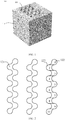
- FIG. 1 and FIG. 2 show schematic diagrams of a semiconductor structure 100 according to an embodiment of the present application.
- FIG. 1 is a three-dimensional view of a semiconductor structure 100
- FIG. 2 is a first pattern 121 formed by projection of at least one trench structure 120 in the semiconductor structure 100 on an upper surface of a substrate 110.
- the semiconductor structure 100 includes a substrate 110 and at least one trench structure 120.
- the substrate 110 includes an upper surface and a lower surface disposed opposite to each other.
- the at least one trench structure 120 is disposed in the substrate 110 and formed downward from the upper surface.
- the trench structure 120 is projected on the upper surface to form a first pattern 121 in a curved or broken line shape, and the first pattern 121 includes n second patterns 122 adjacent to each other, and in the n second patterns 122, odd-numbered second patterns 122 are the same, and even-numbered second patterns 122 are the same, where n is a positive integer.
- the trench structure 120 is a non-linear trench.
- n 10
- second patterns 122 numbered 1, 3, 5, 7 and 9 are the same
- second patterns 122 numbered 2, 4, 6, 8 and 10 are the same.
- serial numbers of the second patterns 122 are assigned for a better understanding of the solution, and the present application is not limited thereto.
- sharp corners are removed from the second pattern 122 numbered 1 and the second pattern 122 numbered 10.
- a device for example, an energy storage device
- the odd-numbered second pattern 122 is rotatable to obtain the even-numbered second pattern 122, or the even-numbered second pattern 122 is rotatable to obtain the odd-numbered second pattern 122.
- the second pattern 122 numbered 2 is rotatable to obtain the second pattern 122 numbered 3
- the second pattern 122 numbered 3 is rotatable to obtain the second pattern 122 numbered 2.
- first patterns 121 in different trench structures 120 among the at least one trench structure 120 may be the same or different.
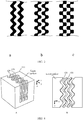
- the first pattern 121 may be one or more of three patterns a, b, and c shown in FIG. 3 .
- the first pattern 121 may also be other regular or irregular patterns, which is not limited in the present application.
- the semiconductor structure 100 may be as shown in FIG. 4 in which A is a perspective view of at least one trench structure 120 in the semiconductor structure 100 according to the embodiment of the present application, and B is a top view of at least one trench structure 120 in the semiconductor structure 100 according to the embodiment of the application.
- x direction represents a width direction of the trench 120
- y direction represents a length direction of the trench 120
- z direction represents a depth direction of the trench 120.
- the semiconductor structure 100 shown in FIG. 4 includes three trench structures 120, and the three trench structures 120 are disposed in the substrate 110 and formed downward from an upper surface of the substrate 110.
- the trench structure 120 is projected on the upper surface of the substrate 110 to form a first pattern 121 in a curved line shape.
- the semiconductor structure 100 is applied to a structure with a high surface area and a low footprint.
- at least one trench structure 120 is etched on the substrate 110 by deep reactive ion etching, which can increase a surface area of the trench structure 120 without increasing an aspect ratio and maintaining the same footprint, for example, increasing the surface area by more than 50%.
- the semiconductor structure 100 is used to produce an energy storage device and/or a sensor, where the energy storage device and/or the sensor includes at least one conductive layer and at least one dielectric layer in the trench structure 120, and the at least one conductive layer and the at least one dielectric layer form a structure in which the conductive layer and the dielectric layer are adjacent to each other.
- a dielectric layer and a conductive layer are alternately deposited in the trench structure 120 to form an energy storage device.
- a dielectric layer and a conductive layer are alternately deposited in the trench structure 120 to form a capacitor.
- the dielectric layer deposited in the trench structure 120 may include at least one of: a silicon dioxide layer, a silicon nitride layer, an aluminum oxide (Al 2 O 3 ) layer, a zirconium oxide (ZrO 2 ) layer, a hafnium oxide (HfO 2 ) layer, a titanium oxide (TiO 2 ) layer, a yttrium oxide (Y 2 O 3 ) layer, a lanthanum oxide (La 2 O 3 ) layer, a hafnium silicate (HfSiO 4 ) layer, a lanthanum aluminate (LaAlO 3 ) layer, a lanthanum lutetium oxide (LaLuO 3 ) layer, a barium titanate (BaTiO 3 ) layer, a strontium titanate (SrTiO 3 ) layer, a barium strontium titanate (Ba x Sr 1-x TiO 3 , B
- a specific insulating material and a dielectric layer thickness may be adjusted according to a capacitance value, a frequency characteristic, a loss and other requirements of a capacitor.
- the dielectric layer may further include some other material layers having high dielectric constant characteristics, which is not limited in the embodiment of the present application.
- the conductive layer deposited in the trench structure 120 includes at least one of: a heavily doped polysilicon layer, a carbon-based material layer, a metal layer, and a titanium nitride layer.
- a specific conductive material may be heavily doped polysilicon, a carbon-based material, or various metals such as aluminum, tungsten and copper, and may also be a low resistivity compound such as titanium nitride (TiN) and tantalum nitride (TaN), or a combination of the above several conductive materials.
- TiN titanium nitride
- TaN tantalum nitride
- the dielectric layer deposited in the trench structure 120 may be a stack of silicon dioxide/aluminum oxide/silicon dioxide (SiO 2 /Al 2 O 3 /SiO 2 ) containing a material with high dielectric constant, so that capacitance density can be improved.
- the substrate 110 may be an n-type or p-type heavily doped low-resistivity silicon wafer.
- a high-resistivity wafer may also be adopted, but after the trench structure 120 is produced, the upper surface (front side) of the substrate 110 and a surface of the trench structure 120 are required to be doped to form a heavily doped low-resistivity conductive layer.
- the at least one trench structure disposed in the substrate is a trench structure in a curved or broken line shape.
- the trench structure in the curved or broken line shape can increase a surface area of the trench structure without increasing an aspect ratio and maintaining the same footprint.
- FIG. 5 is a schematic flow chart of a semiconductor structure production method according to an embodiment of the present application, but these steps or operations are merely examples, and other operations or variations of various operations in FIG. 5 may also be performed in the embodiment of the present application.
- FIG. 5 shows a schematic flow chart of a semiconductor structure production method 200 according to an embodiment of the present application.
- the semiconductor structure production method 200 includes:
- At least one trench structure 120 is etched on a substrate 110 based on a first pattern 121 in a curved or broken line shape to produce the semiconductor structure 100 as shown in FIG. 1 .
- the method 200 further includes: preparing the first pattern.
- the first pattern can be prepared through the following steps.
- Step 1 a linear trench pattern with a length of L and a width of W is provided, where L and W are positive numbers.
- a linear trench pattern 21 has a certain length L and width W, where x direction may be a width direction of the linear trench pattern 21, and y direction may be a length direction of the linear trench pattern 21.
- Step 2 the linear trench pattern is divided into n rectangular patterns adjacent to each other, n is a positive integer, where the rectangular pattern has a first long side and a second long side with a length of L/n in a first direction, and the rectangular pattern has two wide sides with a width of W in a second direction, and the first direction is perpendicular to the second direction.
- the linear trench pattern 21 as shown in a in FIG. 6 is divided into ten rectangular patterns 22 adjacent to each other, as shown in b in FIG. 6 , and the rectangular pattern 22 includes a first long side S1 and a second long side S2 along the y direction, the lengths of the first long side S1 and the second long side S2 are L/n, and the rectangular pattern 22 has two wide sides with a width of W along the x direction, that is, the first direction is the y direction, and the second direction is the x direction.
- the ten rectangular patterns 22 are numbered in the order in which the ten rectangular patterns 22 are formed, and denoted as 1 to 10, respectively.
- first long side S1 and the second long side S2 are formed by two end points and a straight line connecting the two end points.
- the specific number of the divided rectangular patterns 22 adjacent to each other may be determined according to actual requirements, for example, it may be determined according to the length L of the linear trench pattern 21.
- the linear trench pattern 21 is divided into ten rectangular patterns 22 of 1 ⁇ m ⁇ 0.8 ⁇ m.
- Step 3 an odd-numbered rectangular pattern in the n rectangular patterns is divided into two first sub-patterns according to a first dividing line, where the two first sub-patterns include the first long side and the second long side respectively, and the first dividing line connects two end points of the first long side.
- an odd-numbered rectangular pattern 22 (numbered 1, 3, 5, 7 and 9) in the ten rectangular patterns 22 shown in b in FIG. 6 is divided into a first sub-pattern 22A and a first sub-pattern 22B according to a first dividing line 23.
- the first sub-pattern 22A includes the first long side S1
- the first sub-pattern 22B includes the second long side S2
- the first dividing line 23 connects two end points of the first long side S1, as shown in c in FIG. 6 .
- Step 4 the long sides of the two first sub-patterns are overlapped to form N1 first basic patterns, where N1 is a positive integer.
- Step 5 an even-numbered rectangular pattern in the n rectangular patterns is divided into two second sub-patterns according to a second dividing line, where the two second sub-patterns include the first long side and the second long side respectively, and the second dividing line connects two end points of the second long side.
- an even-numbered rectangular pattern 22 (numbered 2, 4, 6, 8 and 10) in the ten rectangular patterns 22 shown in b in FIG. 6 is divided into a second sub-pattern 22C and a second sub-pattern 22D according to a second dividing line 25.
- the second sub-pattern 22C includes the first long side S1
- the second sub-pattern 22D includes the second long side S2
- the second dividing line 25 connects two end points of the second long side S2, as shown in c in FIG. 6 .
- Step 6 the long sides of the two second sub-patterns are overlapped to form N2 second basic patterns, where N2 is a positive integer.
- Step 7 the N1 first basic patterns and the N2 second basic patterns are combined to form the first pattern 121, where the sum of N1 and N2 is n.
- the N1 first basic patterns and the N2 second basic patterns are alternately combined. That is, a first basic pattern can only be combined with a second basic pattern, but cannot be combined with another first basic pattern. Similarly, a second basic pattern can only be combined with a first basic pattern, but cannot be combined with another second basic pattern.
- the five first basic patterns 24 and the five second basic patterns 26 shown in d in FIG. 6 are combined to form the first pattern 121, as shown in e in FIG. 6 .
- the five first basic patterns 24 and the five second basic patterns 26 may be randomly combined.
- the first basic pattern 24 numbered 1 is combined with the second basic pattern 26 numbered 6
- the second basic pattern 26 numbered 6 is combined with the first basic pattern 24 numbered 3
- the second basic pattern 26 numbered 2 is combined with the first basic pattern 24 numbered 5
- the first basic pattern 24 numbered 5 is combined with the second basic pattern 26 numbered 8
- the second basic pattern 26 numbered 8 is combined with the first basic pattern 24 numbered 7
- the first basic pattern 24 numbered 7 is combined with the second basic pattern 26 numbered 10
- the second basic pattern 26 numbered 10 is combined with the first basic pattern 24 numbered 9
- the five first basic patterns 24 and the five second basic patterns 26 may be combined in a certain order.
- the first basic pattern 24 numbered 1 is combined with the second basic pattern 26 numbered 2
- the second basic pattern 26 numbered 2 is combined with the first basic pattern 24 numbered 3
- the first basic pattern 24 numbered 3 is combined with the second basic pattern 26 numbered 4
- the second basic pattern 26 numbered 4 is combined with the first basic pattern 24 numbered 5
- the first basic pattern 24 numbered 5 is combined with the second basic pattern 26 numbered 6
- the second basic pattern 26 numbered 6 is combined with the first basic pattern 24 numbered 7
- the first basic pattern 24 numbered 7 is combined with the second basic pattern 26 numbered 8
- the second basic pattern 26 numbered 8 is combined with the first basic pattern 24 numbered 9
- the serial number of the first basic pattern 24 is the serial number of the corresponding rectangular pattern 22.
- the rectangular pattern 22 numbered 1 is divided and combined to form the first basic pattern 24 numbered 1
- the rectangular pattern 22 numbered 3 is divided and combined to form the first basic pattern 24 numbered 3
- the rectangular pattern 22 numbered 5 is divided and combined to form the first basic pattern 24 numbered 5
- the rectangular pattern 22 numbered 7 is divided and combined to form the first basic pattern 24 numbered 7
- the rectangular pattern 22 numbered 9 is divided and combined to form the first basic pattern 24 numbered 9.
- the serial number of the second basic pattern 26 is the serial number of the corresponding rectangular pattern 22.
- the rectangular pattern 22 numbered 2 is divided and combined to form the second basic pattern 26 numbered 2
- the rectangular pattern 22 numbered 4 is divided and combined to form the second basic pattern 26 numbered 4
- the rectangular pattern 22 numbered 6 is divided and combined to form the second basic pattern 26 numbered 6
- the rectangular pattern 22 numbered 8 is divided and combined to form the second basic pattern 26 numbered 8
- the rectangular pattern 22 numbered 10 is divided and combined to form the second basic pattern 26 numbered 10.
- first basic pattern 24 and the second basic pattern 26 may be combined along the side in the x direction.
- the at least one trench structure 120 may be etched on the substrate 110 by deep reactive ion etching based on the first pattern 121.
- a layer of photoresist is spin-coated on the upper surface (front side) of the substrate 110 based on the first pattern 121, and after exposure and development, an etched pattern window not covered with the photoresist is formed.
- at least one trench structure 120 is produced in the substrate 110 by deep reactive ion etching. The trench structure 120 extends downward from the upper surface of the substrate 110, and a depth of the trench structure 120 is less than a thickness of the substrate 110.
- execution orders of the above steps 3 and 4 can be interchanged with those of the above steps 5 and 6, that is, the odd-numbered rectangular patterns can be processed first to form the N1 first basic patterns, or the even-numbered rectangular patterns can also be processed first to form the N2 second basic patterns.
- the area of the first pattern 121 is exactly the same as that of the original linear trench pattern 21, and therefore the footprint remains unchanged.
- the perimeter of the first pattern 121 is greater than that of the linear trench pattern 21, and perimeter multiplied by depth equals surface area, and thus the surface area is increased.
- the perimeter of the first pattern 121 is approximately 1.57 times that of the linear trench pattern 21, and thus the resulting surface area of the trench structure 120 can also be increased by 57%.
- a non-linear trench pattern can be formed based on a linear trench pattern, so that a non-linear trench structure can be etched on a substrate based on the non-linear trench pattern, which can increase a surface area of the trench structure without increasing an aspect ratio and maintaining the same footprint.
- the method 200 further includes: removing sharp corners at head and tail ends of the first pattern 121.
- sharp corners at head and tail ends of the first pattern 121 as shown in e in FIG. 6 are removed, as shown in f in FIG. 6 .
- sharp corners less than 90 degrees at the head and tail ends of the first pattern 121 are removed.
- the first pattern 121 when the first pattern 121 is used to produce a device (for example, an energy storage device), it is possible to avoid the formation of an area where an electric field is too concentrated at the sharp corners, thereby ensuring the performance of the produced device.
- a device for example, an energy storage device
- the sharp corners at the head and tail ends of the first pattern 121 may be removed by cutting, erasing, or the like.
- the sharp corners at the head and tail ends of the first pattern 121 may also be removed in other ways, which is not limited in the present application.
- the first dividing line 23 and/or the second dividing line 25 is at least one curve and/or at least one broken line.
- the first dividing line 23 and the second dividing line 25 are broken lines, and a non-linear trench pattern (a first pattern) shown in FIG. 7 is formed based on the above semiconductor structure production method 200.
- the first dividing line 23 and the second dividing line 25 are curves, and a non-linear trench pattern (a first pattern) shown in FIG. 8 is formed based on the above semiconductor structure production method 200.
- the first dividing line 23 and the second dividing line 25 are also curves, and a non-linear trench pattern (a first pattern) shown in FIG. 9 is formed based on the above semiconductor structure production method 200.
- the first dividing line 23 and the second dividing line 25 are also curves, and a non-linear trench pattern (a first pattern) shown in FIG. 10 is formed based on the above semiconductor structure production method 200.
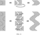
- the first dividing line 23 and the second dividing line 25 are also multiple broken lines, and a non-linear trench pattern (a first pattern) shown in FIG. 11 is formed based on the above semiconductor structure production method 200.
- the first dividing line 23 and the second dividing line 25 are symmetrical with an axis of the linear trench pattern being a symmetry axis.
- the first basic pattern 24 is rotatable to obtain the second basic pattern 26, or the second basic pattern 26 is rotatable to obtain the first basic pattern 24.
- the first dividing line 23 and the second dividing line 25 may also be different.
- the first dividing line 23 is a broken line
- the second dividing line 25 is a curve.
- a non-linear trench pattern can be formed based on a linear trench pattern, so that a non-linear trench structure can be etched on a substrate based on the non-linear trench pattern, which can increase a surface area of the trench structure without increasing an aspect ratio and maintaining the same footprint.
- At least one insulating layer and at least one conductive layer may be alternately deposited in the at least one trench structure 120 to produce a capacitor.
- silicon dioxide is deposited (grown) on the upper surface of the substrate 110 and the inner surface of the at least one trench structure 120 as the insulating layer.
- silicon dioxide or silicon nitride is grown by physical vapor deposition (Physical Vapor Deposition, PVD) or chemical vapor deposition (Chemical Vapor Deposition, CVD).
- a thin film of high dielectric constant material is grown by an atomic layer deposition (Atomic layer deposition, ALD) process, such as Al 2 O 3 , HfO 2 , ZrO 2 , TiO 2 , Y 2 O 3 , La 2 O 3 , HfSiO 4 , LaAlO 3 , BaTiO 3 , SrTiO 3 , LaLuO 3 , BST, PZT, and CCTO.
- ALD atomic layer deposition
- a material of the insulating layer includes a silicon oxide, a silicon nitride, a metal oxide, a metal nitride, or the like, such as silicon dioxide, silicon nitride, aluminum oxide, aluminum nitride, hafnium oxide, zirconium oxide, zinc oxide, titanium oxide, yttrium oxide, lanthanum oxide, hafnium silicate, lanthanum aluminate, lanthanum lutetium oxide, barium titanate, strontium titanate, barium strontium titanate, calcium copper titanate, lead zirconate titanate, etc.
- the insulating layer may be single-layered, or two or multi-layered. A specific material and a layer thickness may be adjusted according to a capacitance value, a frequency characteristic, a loss and other requirements of a capacitor.
- a method of depositing the conductive layer includes ALD, PVD, metal-organic chemical vapor deposition, evaporation, electroplating, or the like.
- a conductive material of the conductive layer may be heavily doped polysilicon, a carbon-based material, or various metals such as aluminum, tungsten and copper, and may also be a low resistivity compound such as titanium nitride, or a combination of the above several conductive materials.
- the conductive layer may include at least one of: a heavily doped polysilicon layer, a carbon-based material layer, a metal layer, and a titanium nitride layer.
Landscapes
- Semiconductor Integrated Circuits (AREA)
- Physics & Mathematics (AREA)
- Engineering & Computer Science (AREA)
- Plasma & Fusion (AREA)
- Drying Of Semiconductors (AREA)
Abstract
Description
- The present application relates to the field of semiconductors, and more particularly, to a semiconductor structure and a production method thereof.
- As an energy storage device (for example, a battery, a capacitor, etc.), a sensor, or the like are widely used in modern electronic systems, it is necessary to produce a structure with a high surface area and a low footprint to increase an energy density and a sensing area.
- Using plasma etching technology to produce a trench with a high aspect ratio on a substrate is a widely used method to increase a surface area. However, due to the characteristics of plasma etching technology, processing a structure with a high aspect ratio has greater process difficulty. To put it simply, as etching progresses to a certain depth, on the one hand, it is difficult for a reactive substance participating in the etching to continue to enter the bottom of a trench, and on the other hand, it is difficult for a product generated in the reaction to diffuse out from the bottom of the trench. The smaller the trench opening is, the greater the trench depth is, and the more serious this phenomenon is. Therefore, using the existing etching technology to produce a structure with a higher aspect ratio easily leads to process problems such as low etching efficiency, poor etching uniformity, and poor repeatability. In addition, apart from the above-mentioned problems of the etching itself, the difficulty of performing subsequent processes on the structure with a higher aspect ratio is correspondingly increased. The resulting series of problems such as yield, output, and costs are difficult to be solved. Therefore, how to produce a structure with a high surface area and a low footprint is an urgent technical problem to be solved.
- The present application provides a semiconductor structure and a production method thereof so that a non-linear trench structure can be produced, which can increase a surface area of the trench structure without increasing an aspect ratio and maintaining the same footprint.
- According to a first aspect, provided is a semiconductor structure, including:
- a substrate including an upper surface and a lower surface disposed opposite to each other; and
- at least one trench structure disposed in the substrate and formed downward from the upper surface,
- where the trench structure is projected on the upper surface to form a first pattern in a curved or broken line shape, and the first pattern includes n second patterns adjacent to each other, and in the n second patterns, odd-numbered second patterns are the same, and even-numbered second patterns are the same, where n is a positive integer.
- Therefore, in the semiconductor structure provided by the embodiment of the present application, compared to a linear trench structure, the at least one trench structure in the curved or broken line shape disposed in the substrate can increase a surface area of the trench structure without increasing an aspect ratio and maintaining the same footprint.
- In some possible implementation manners, the odd-numbered second pattern is rotatable to obtain the even-numbered second pattern, or the even-numbered second pattern is rotatable to obtain the odd-numbered second pattern.
- In some possible implementation manners, the semiconductor structure is used to produce a structure with a high surface area and a low footprint.
- In some possible implementation manners, the semiconductor structure is used to produce an energy storage device and/or a sensor, where the energy storage device and/or the sensor includes at least one conductive layer and at least one dielectric layer in the trench structure.
- Therefore, when the semiconductor structure of the embodiment of the present application is applied to an energy storage device and/or a sensor, an energy density of the energy storage device and a sensing area of the sensor can be increased.
- In a second aspect, provided is a semiconductor structure production method, including:
- providing a substrate including an upper surface and a lower surface disposed opposite to each other; and
- etching at least one trench structure on the substrate based on a first pattern in a curved or broken line shape, the trench structure entering the substrate downward from the upper surface, where the first pattern includes n second patterns adjacent to each other, and in the n second patterns, odd-numbered second patterns are the same, and even-numbered second patterns are the same, where n is a positive integer.
- Therefore, in the embodiment of the present application, the trench structure in the curved or broken line shape can be etched on the substrate based on the first pattern in the curved or broken line shape, which can increase a surface area of the trench structure without increasing an aspect ratio and maintaining the same footprint.
- In some possible implementation manners, before the etching the at least one trench structure, the method further includes:
- providing a linear trench pattern with a length of L and a width of W, where L and W are positive numbers;
- dividing the linear trench pattern into n rectangular patterns adjacent to each other, where the rectangular pattern has a first long side and a second long side with a length of L/n in a first direction, and the rectangular pattern has two wide sides with a width of W in a second direction, and the first direction is perpendicular to the second direction;
- dividing an odd-numbered rectangular pattern in the n rectangular patterns into two first sub-patterns according to a first dividing line, where the two first sub-patterns include the first long side and the second long side respectively, and the first dividing line connects two end points of the first long side;
- overlapping the long sides of the two first sub-patterns to form N1 first basic patterns, where N1 is a positive integer;
- dividing an even-numbered rectangular pattern in the n rectangular patterns into two second sub-patterns according to a second dividing line, where the two second sub-patterns include the first long side and the second long side respectively, and the second dividing line connects two end points of the second long side;
- overlapping the long sides of the two second sub-patterns to form N2 second basic patterns, where N2 is a positive integer; and
- combining the N1 first basic patterns and the N2 second basic patterns to form the first pattern, where the sum of N1 and N2 is n.
- It should be noted that the area of the first pattern is exactly the same as that of the original linear trench pattern, and therefore the footprint remains unchanged. The perimeter of the first pattern is greater than that of the linear trench pattern, and perimeter multiplied depth equals surface area, and thus the surface area is increased.
- In some possible implementation manners, before the etching the at least one trench structure, the method further includes:
removing sharp corners at head and tail ends of the first pattern. - It should be noted that by removing the sharp corners at the head and tail ends of the first pattern, when the first pattern is used to produce a device (for example, an energy storage device), it is possible to avoid the formation of an area where an electric field is too concentrated at the sharp corners, thereby ensuring the performance of the produced device.
- In some possible implementation manners, the removing the sharp corners at the head and tail ends of the first pattern includes:
removing sharp corners less than 90 degrees at the head and tail ends of the first pattern. - In some possible implementation manners, the first dividing line and/or the second dividing line is at least one curve and/or at least one broken line.
- In some possible implementation manners, the first dividing line and the second dividing line are symmetrical with an axis of the linear trench pattern being a symmetry axis.
- In some possible implementation manners, the first basic pattern is rotatable to obtain the second basic pattern, or the second basic pattern is rotatable to obtain the first basic pattern.
- In some possible implementation manners, the etching the at least one trench structure on the substrate based on the first pattern in the curved or broken line shape includes:
etching the at least one trench structure on the substrate by deep reactive ion etching (deep reactive ion etching, DRIE) based on the first pattern. -
-
FIG. 1 and FIG. 2 show schematic diagrams of asemiconductor structure 100 according to an embodiment of the present application. -
FIG. 3 is a schematic diagram of afirst pattern 121 according to an embodiment of the present application. -
FIG. 4 is a schematic diagram of asemiconductor structure 100 according to an embodiment of the present application. -
FIG. 5 shows a schematic flow chart of a semiconductorstructure production method 200 according to an embodiment of the present application. -
FIG. 6 is a schematic diagram of a semiconductor structure production method according to an embodiment of the present application. -
FIG. 7 is a schematic diagram of another semiconductor structure production method according to an embodiment of the present application. -
FIG. 8 is a schematic diagram of another semiconductor structure production method according to an embodiment of the present application. -
FIG. 9 is a schematic diagram of yet another semiconductor structure production method according to an embodiment of the present application. -
FIG. 10 is a schematic diagram of yet another semiconductor structure production method according to an embodiment of the present application. -
FIG. 11 is a schematic diagram of yet another semiconductor structure production method according to an embodiment of the present application. - Technical solutions in embodiments of the present application will be described hereinafter in conjunction with the accompanying drawings.
-
FIG. 1 and FIG. 2 show schematic diagrams of asemiconductor structure 100 according to an embodiment of the present application. -
FIG. 1 is a three-dimensional view of asemiconductor structure 100, andFIG. 2 is afirst pattern 121 formed by projection of at least onetrench structure 120 in thesemiconductor structure 100 on an upper surface of asubstrate 110. - As shown in
FIG. 1 , thesemiconductor structure 100 includes asubstrate 110 and at least onetrench structure 120. - The
substrate 110 includes an upper surface and a lower surface disposed opposite to each other. - The at least one
trench structure 120 is disposed in thesubstrate 110 and formed downward from the upper surface. - As shown in
FIG. 2 , thetrench structure 120 is projected on the upper surface to form afirst pattern 121 in a curved or broken line shape, and thefirst pattern 121 includes nsecond patterns 122 adjacent to each other, and in the nsecond patterns 122, odd-numberedsecond patterns 122 are the same, and even-numberedsecond patterns 122 are the same, where n is a positive integer. - That is, in the embodiment of the present application, the
trench structure 120 is a non-linear trench. - Specifically, as shown in
FIG. 2 , n is 10,second patterns 122 numbered 1, 3, 5, 7 and 9 (odd digits) are the same, andsecond patterns 122 numbered 2, 4, 6, 8 and 10 (even digits) are the same. It should be noted that the serial numbers of thesecond patterns 122 are assigned for a better understanding of the solution, and the present application is not limited thereto. - It should be noted that sharp corners are removed from the
second pattern 122 numbered 1 and thesecond pattern 122 numbered 10. By removing the sharp corners at head and tail ends of thetrench structure 120, when thetrench structure 120 is used to produce a device (for example, an energy storage device), it is possible to avoid the formation of an area where an electric field is too concentrated at the sharp corners, thereby ensuring the performance of the produced device. - Of course, in the embodiment of the present application, it is also not necessary to remove the sharp corners at head and tail ends of the
trench structure 120. - Optionally, the odd-numbered
second pattern 122 is rotatable to obtain the even-numberedsecond pattern 122, or the even-numberedsecond pattern 122 is rotatable to obtain the odd-numberedsecond pattern 122. For example, as shown inFIG. 2 , thesecond pattern 122 numbered 2 is rotatable to obtain thesecond pattern 122 numbered 3, and of course, thesecond pattern 122 numbered 3 is rotatable to obtain thesecond pattern 122 numbered 2. - Optionally, in the embodiment of the present application,
first patterns 121 indifferent trench structures 120 among the at least onetrench structure 120 may be the same or different. - For example, the
first pattern 121 may be one or more of three patterns a, b, and c shown inFIG. 3 . Of course, thefirst pattern 121 may also be other regular or irregular patterns, which is not limited in the present application. - Optionally, in the embodiment of the present application, the
semiconductor structure 100 may be as shown inFIG. 4 in which A is a perspective view of at least onetrench structure 120 in thesemiconductor structure 100 according to the embodiment of the present application, and B is a top view of at least onetrench structure 120 in thesemiconductor structure 100 according to the embodiment of the application. And inFIG. 4 , x direction represents a width direction of thetrench 120, y direction represents a length direction of thetrench 120, and z direction represents a depth direction of thetrench 120. Thesemiconductor structure 100 shown inFIG. 4 includes threetrench structures 120, and the threetrench structures 120 are disposed in thesubstrate 110 and formed downward from an upper surface of thesubstrate 110. Thetrench structure 120 is projected on the upper surface of thesubstrate 110 to form afirst pattern 121 in a curved line shape. - Optionally, in the embodiment of the present application, the
semiconductor structure 100 is applied to a structure with a high surface area and a low footprint. For example, based on the non-linearfirst pattern 121, at least onetrench structure 120 is etched on thesubstrate 110 by deep reactive ion etching, which can increase a surface area of thetrench structure 120 without increasing an aspect ratio and maintaining the same footprint, for example, increasing the surface area by more than 50%. - Optionally, the
semiconductor structure 100 is used to produce an energy storage device and/or a sensor, where the energy storage device and/or the sensor includes at least one conductive layer and at least one dielectric layer in thetrench structure 120, and the at least one conductive layer and the at least one dielectric layer form a structure in which the conductive layer and the dielectric layer are adjacent to each other. - For example, a dielectric layer and a conductive layer are alternately deposited in the
trench structure 120 to form an energy storage device. - Optionally, as an example, a dielectric layer and a conductive layer are alternately deposited in the
trench structure 120 to form a capacitor. - It should be noted that, in this example, the dielectric layer deposited in the
trench structure 120 may include at least one of: a silicon dioxide layer, a silicon nitride layer, an aluminum oxide (Al2O3) layer, a zirconium oxide (ZrO2) layer, a hafnium oxide (HfO2) layer, a titanium oxide (TiO2) layer, a yttrium oxide (Y2O3) layer, a lanthanum oxide (La2O3) layer, a hafnium silicate (HfSiO4) layer, a lanthanum aluminate (LaAlO3) layer, a lanthanum lutetium oxide (LaLuO3) layer, a barium titanate (BaTiO3) layer, a strontium titanate (SrTiO3) layer, a barium strontium titanate (BaxSr1-xTiO3, BST) layer, a lead zirconate titanate (PbZrxTi1-xO3, PZT) layer, and a calcium copper titanate (CaCu3Ti4O12, CCTO) layer. A specific insulating material and a dielectric layer thickness may be adjusted according to a capacitance value, a frequency characteristic, a loss and other requirements of a capacitor. Of course, the dielectric layer may further include some other material layers having high dielectric constant characteristics, which is not limited in the embodiment of the present application. The conductive layer deposited in thetrench structure 120 includes at least one of: a heavily doped polysilicon layer, a carbon-based material layer, a metal layer, and a titanium nitride layer. A specific conductive material may be heavily doped polysilicon, a carbon-based material, or various metals such as aluminum, tungsten and copper, and may also be a low resistivity compound such as titanium nitride (TiN) and tantalum nitride (TaN), or a combination of the above several conductive materials. - The dielectric layer deposited in the
trench structure 120 may be a stack of silicon dioxide/aluminum oxide/silicon dioxide (SiO2/Al2O3/SiO2) containing a material with high dielectric constant, so that capacitance density can be improved. - Optionally, in the embodiment of the present application, the
substrate 110 may be an n-type or p-type heavily doped low-resistivity silicon wafer. A high-resistivity wafer may also be adopted, but after thetrench structure 120 is produced, the upper surface (front side) of thesubstrate 110 and a surface of thetrench structure 120 are required to be doped to form a heavily doped low-resistivity conductive layer. - Therefore, in the semiconductor structure provided by the embodiment of the present application, the at least one trench structure disposed in the substrate is a trench structure in a curved or broken line shape. Compared with a linear trench structure, the trench structure in the curved or broken line shape can increase a surface area of the trench structure without increasing an aspect ratio and maintaining the same footprint.
- Hereinafter, a semiconductor structure production method according to an embodiment of the present application will be introduced in detail with reference to
FIGS. 5 to 11 . - It should be understood that
FIG. 5 is a schematic flow chart of a semiconductor structure production method according to an embodiment of the present application, but these steps or operations are merely examples, and other operations or variations of various operations inFIG. 5 may also be performed in the embodiment of the present application. -
FIG. 5 shows a schematic flow chart of a semiconductorstructure production method 200 according to an embodiment of the present application. As shown inFIG. 5 , the semiconductorstructure production method 200 includes: - S210, providing a substrate including an upper surface and a lower surface disposed opposite to each other; and
- S220, etching at least one trench structure on the substrate based on a first pattern in a curved or broken line shape, the trench structure entering the substrate downward from the upper surface, where the first pattern includes n second patterns adjacent to each other, and in the n second patterns, odd-numbered second patterns are the same, and even-numbered second patterns are the same, where n is a positive integer.
- Specifically, at least one
trench structure 120 is etched on asubstrate 110 based on afirst pattern 121 in a curved or broken line shape to produce thesemiconductor structure 100 as shown inFIG. 1 . - Optionally, before the etching the at least one trench structure, the
method 200 further includes:
preparing the first pattern. - Specifically, the first pattern can be prepared through the following steps.
- Step 1, a linear trench pattern with a length of L and a width of W is provided, where L and W are positive numbers.
- Specifically, as shown in a in
FIG. 6 , alinear trench pattern 21 has a certain length L and width W, where x direction may be a width direction of thelinear trench pattern 21, and y direction may be a length direction of thelinear trench pattern 21. -
Step 2, the linear trench pattern is divided into n rectangular patterns adjacent to each other, n is a positive integer, where the rectangular pattern has a first long side and a second long side with a length of L/n in a first direction, and the rectangular pattern has two wide sides with a width of W in a second direction, and the first direction is perpendicular to the second direction. - Specifically, the
linear trench pattern 21 as shown in a inFIG. 6 is divided into tenrectangular patterns 22 adjacent to each other, as shown in b inFIG. 6 , and therectangular pattern 22 includes a first long side S1 and a second long side S2 along the y direction, the lengths of the first long side S1 and the second long side S2 are L/n, and therectangular pattern 22 has two wide sides with a width of W along the x direction, that is, the first direction is the y direction, and the second direction is the x direction. As shown in b inFIG. 6 , the tenrectangular patterns 22 are numbered in the order in which the tenrectangular patterns 22 are formed, and denoted as 1 to 10, respectively. - It should be noted that the first long side S1 and the second long side S2 are formed by two end points and a straight line connecting the two end points.
- It should be understood that the specific number of the divided
rectangular patterns 22 adjacent to each other may be determined according to actual requirements, for example, it may be determined according to the length L of thelinear trench pattern 21. - Assuming that the length L and the width W of the
linear trench pattern 21 are 10 µm and 0.8 µm, respectively, thelinear trench pattern 21 is divided into tenrectangular patterns 22 of 1 µm × 0.8 µm. -
Step 3, an odd-numbered rectangular pattern in the n rectangular patterns is divided into two first sub-patterns according to a first dividing line, where the two first sub-patterns include the first long side and the second long side respectively, and the first dividing line connects two end points of the first long side. - Specifically, an odd-numbered rectangular pattern 22 (numbered 1, 3, 5, 7 and 9) in the ten
rectangular patterns 22 shown in b inFIG. 6 is divided into a first sub-pattern 22A and a first sub-pattern 22B according to afirst dividing line 23. The first sub-pattern 22A includes the first long side S1, the first sub-pattern 22B includes the second long side S2, and thefirst dividing line 23 connects two end points of the first long side S1, as shown in c inFIG. 6 . -
Step 4, the long sides of the two first sub-patterns are overlapped to form N1 first basic patterns, where N1 is a positive integer. - Specifically, the first long side S1 included in the first sub-pattern 22A and the second long side S2 included in the first sub-pattern 22B as shown in c in
FIG. 6 are overlapped to form five firstbasic patterns 24, that is, N1=5, as shown in d inFIG. 6 . - Step 5, an even-numbered rectangular pattern in the n rectangular patterns is divided into two second sub-patterns according to a second dividing line, where the two second sub-patterns include the first long side and the second long side respectively, and the second dividing line connects two end points of the second long side.
- Specifically, an even-numbered rectangular pattern 22 (numbered 2, 4, 6, 8 and 10) in the ten
rectangular patterns 22 shown in b inFIG. 6 is divided into a second sub-pattern 22C and a second sub-pattern 22D according to asecond dividing line 25. The second sub-pattern 22C includes the first long side S1, the second sub-pattern 22D includes the second long side S2, and thesecond dividing line 25 connects two end points of the second long side S2, as shown in c inFIG. 6 . -
Step 6, the long sides of the two second sub-patterns are overlapped to form N2 second basic patterns, where N2 is a positive integer. - Specifically, the first long side S1 included in the second sub-pattern 22C and the second long side S2 included in the second sub-pattern 22D as shown in c in
FIG. 6 are overlapped to form five secondbasic patterns 26, that is, N2=5, as shown in d inFIG. 6 . -
Step 7, the N1 first basic patterns and the N2 second basic patterns are combined to form thefirst pattern 121, where the sum of N1 and N2 is n. - Optionally, the N1 first basic patterns and the N2 second basic patterns are alternately combined. That is, a first basic pattern can only be combined with a second basic pattern, but cannot be combined with another first basic pattern. Similarly, a second basic pattern can only be combined with a first basic pattern, but cannot be combined with another second basic pattern.
- Specifically, the five first
basic patterns 24 and the five secondbasic patterns 26 shown in d inFIG. 6 are combined to form thefirst pattern 121, as shown in e inFIG. 6 . - Optionally, the five first
basic patterns 24 and the five secondbasic patterns 26 may be randomly combined. - For example, the first
basic pattern 24 numbered 1 is combined with the secondbasic pattern 26 numbered 6, the secondbasic pattern 26 numbered 6 is combined with the firstbasic pattern 24 numbered 3, the firstbasic pattern 24 numbered 3 is combined with the secondbasic pattern 26 numbered 2, the secondbasic pattern 26 numbered 2 is combined with the firstbasic pattern 24 numbered 5, the firstbasic pattern 24 numbered 5 is combined with the secondbasic pattern 26 numbered 8, the secondbasic pattern 26 numbered 8 is combined with the firstbasic pattern 24 numbered 7, the firstbasic pattern 24 numbered 7 is combined with the secondbasic pattern 26 numbered 10, the secondbasic pattern 26 numbered 10 is combined with the firstbasic pattern 24 numbered 9, or the firstbasic pattern 24 numbered 9 is combined with the secondbasic pattern 26 numbered 4. - Optionally, the five first
basic patterns 24 and the five secondbasic patterns 26 may be combined in a certain order. - For example, the first
basic pattern 24 numbered 1 is combined with the secondbasic pattern 26 numbered 2, the secondbasic pattern 26 numbered 2 is combined with the firstbasic pattern 24 numbered 3, the firstbasic pattern 24 numbered 3 is combined with the secondbasic pattern 26 numbered 4, the secondbasic pattern 26 numbered 4 is combined with the firstbasic pattern 24 numbered 5, the firstbasic pattern 24 numbered 5 is combined with the secondbasic pattern 26 numbered 6, the secondbasic pattern 26 numbered 6 is combined with the firstbasic pattern 24 numbered 7, the firstbasic pattern 24 numbered 7 is combined with the secondbasic pattern 26 numbered 8, the secondbasic pattern 26 numbered 8 is combined with the firstbasic pattern 24 numbered 9, or the firstbasic pattern 24 numbered 9 is combined with the secondbasic pattern 26 numbered 10. - It should be understood that the serial number of the first
basic pattern 24 is the serial number of the correspondingrectangular pattern 22. For example, therectangular pattern 22 numbered 1 is divided and combined to form the firstbasic pattern 24 numbered 1, therectangular pattern 22 numbered 3 is divided and combined to form the firstbasic pattern 24 numbered 3, therectangular pattern 22 numbered 5 is divided and combined to form the firstbasic pattern 24 numbered 5, therectangular pattern 22 numbered 7 is divided and combined to form the firstbasic pattern 24 numbered 7, and therectangular pattern 22 numbered 9 is divided and combined to form the firstbasic pattern 24 numbered 9. Similarly, the serial number of the secondbasic pattern 26 is the serial number of the correspondingrectangular pattern 22. For example, therectangular pattern 22 numbered 2 is divided and combined to form the secondbasic pattern 26 numbered 2, therectangular pattern 22 numbered 4 is divided and combined to form the secondbasic pattern 26 numbered 4, therectangular pattern 22 numbered 6 is divided and combined to form the secondbasic pattern 26 numbered 6, therectangular pattern 22 numbered 8 is divided and combined to form the secondbasic pattern 26 numbered 8, and therectangular pattern 22 numbered 10 is divided and combined to form the secondbasic pattern 26 numbered 10. - It should be noted that the first
basic pattern 24 and the secondbasic pattern 26 may be combined along the side in the x direction. - Optionally, the at least one
trench structure 120 may be etched on thesubstrate 110 by deep reactive ion etching based on thefirst pattern 121. - Specifically, first, a layer of photoresist is spin-coated on the upper surface (front side) of the
substrate 110 based on thefirst pattern 121, and after exposure and development, an etched pattern window not covered with the photoresist is formed. Next, at least onetrench structure 120 is produced in thesubstrate 110 by deep reactive ion etching. Thetrench structure 120 extends downward from the upper surface of thesubstrate 110, and a depth of thetrench structure 120 is less than a thickness of thesubstrate 110. - It should be understood that after etching the at least one
trench structure 120, the photoresist is removed. - It should be noted that the execution orders of the
above steps above steps 5 and 6, that is, the odd-numbered rectangular patterns can be processed first to form the N1 first basic patterns, or the even-numbered rectangular patterns can also be processed first to form the N2 second basic patterns. - In the semiconductor
structure production method 200 described above, the area of thefirst pattern 121 is exactly the same as that of the originallinear trench pattern 21, and therefore the footprint remains unchanged. The perimeter of thefirst pattern 121 is greater than that of thelinear trench pattern 21, and perimeter multiplied by depth equals surface area, and thus the surface area is increased. For example, the perimeter of thefirst pattern 121 is approximately 1.57 times that of thelinear trench pattern 21, and thus the resulting surface area of thetrench structure 120 can also be increased by 57%. - Therefore, in the embodiment of the present application, a non-linear trench pattern can be formed based on a linear trench pattern, so that a non-linear trench structure can be etched on a substrate based on the non-linear trench pattern, which can increase a surface area of the trench structure without increasing an aspect ratio and maintaining the same footprint.
- Optionally, before the etching the at least one
trench structure 120, themethod 200 further includes:
removing sharp corners at head and tail ends of thefirst pattern 121. - Specifically, sharp corners at head and tail ends of the
first pattern 121 as shown in e inFIG. 6 are removed, as shown in f inFIG. 6 . - For example, sharp corners less than 90 degrees at the head and tail ends of the
first pattern 121 are removed. - It should be noted that by removing the sharp corners at the head and tail ends of the
first pattern 121, when thefirst pattern 121 is used to produce a device (for example, an energy storage device), it is possible to avoid the formation of an area where an electric field is too concentrated at the sharp corners, thereby ensuring the performance of the produced device. - It should also be noted that the sharp corners at the head and tail ends of the
first pattern 121 may be removed by cutting, erasing, or the like. Of course, the sharp corners at the head and tail ends of thefirst pattern 121 may also be removed in other ways, which is not limited in the present application. - In some possible implementation manners, the
first dividing line 23 and/or thesecond dividing line 25 is at least one curve and/or at least one broken line. - For example, as shown in
FIG. 7 , thefirst dividing line 23 and thesecond dividing line 25 are broken lines, and a non-linear trench pattern (a first pattern) shown inFIG. 7 is formed based on the above semiconductorstructure production method 200. - For another example, as shown in
FIG. 8 , thefirst dividing line 23 and thesecond dividing line 25 are curves, and a non-linear trench pattern (a first pattern) shown inFIG. 8 is formed based on the above semiconductorstructure production method 200. - For another example, as shown in
FIG. 9 , thefirst dividing line 23 and thesecond dividing line 25 are also curves, and a non-linear trench pattern (a first pattern) shown inFIG. 9 is formed based on the above semiconductorstructure production method 200. - For yet another example, as shown in
FIG. 10 , thefirst dividing line 23 and thesecond dividing line 25 are also curves, and a non-linear trench pattern (a first pattern) shown inFIG. 10 is formed based on the above semiconductorstructure production method 200. - For yet another example, as shown in
FIG. 11 , thefirst dividing line 23 and thesecond dividing line 25 are also multiple broken lines, and a non-linear trench pattern (a first pattern) shown inFIG. 11 is formed based on the above semiconductorstructure production method 200. - It should be noted that during the formation of the non-linear trench pattern shown in
FIGS. 7 to 11 , thefirst dividing line 23 and thesecond dividing line 25 are symmetrical with an axis of the linear trench pattern being a symmetry axis. The firstbasic pattern 24 is rotatable to obtain the secondbasic pattern 26, or the secondbasic pattern 26 is rotatable to obtain the firstbasic pattern 24. Of course, thefirst dividing line 23 and thesecond dividing line 25 may also be different. For example, thefirst dividing line 23 is a broken line, and thesecond dividing line 25 is a curve. - Therefore, in the embodiment of the present application, a non-linear trench pattern can be formed based on a linear trench pattern, so that a non-linear trench structure can be etched on a substrate based on the non-linear trench pattern, which can increase a surface area of the trench structure without increasing an aspect ratio and maintaining the same footprint.
- Optionally, as an example, at least one insulating layer and at least one conductive layer may be alternately deposited in the at least one
trench structure 120 to produce a capacitor. - For example, by means of thermal oxidation, silicon dioxide is deposited (grown) on the upper surface of the
substrate 110 and the inner surface of the at least onetrench structure 120 as the insulating layer. For another example, silicon dioxide or silicon nitride is grown by physical vapor deposition (Physical Vapor Deposition, PVD) or chemical vapor deposition (Chemical Vapor Deposition, CVD). For another example, a thin film of high dielectric constant material is grown by an atomic layer deposition (Atomic layer deposition, ALD) process, such as Al2O3, HfO2, ZrO2, TiO2, Y2O3, La2O3, HfSiO4, LaAlO3, BaTiO3, SrTiO3, LaLuO3, BST, PZT, and CCTO. - It should be noted that a material of the insulating layer includes a silicon oxide, a silicon nitride, a metal oxide, a metal nitride, or the like, such as silicon dioxide, silicon nitride, aluminum oxide, aluminum nitride, hafnium oxide, zirconium oxide, zinc oxide, titanium oxide, yttrium oxide, lanthanum oxide, hafnium silicate, lanthanum aluminate, lanthanum lutetium oxide, barium titanate, strontium titanate, barium strontium titanate, calcium copper titanate, lead zirconate titanate, etc. The insulating layer may be single-layered, or two or multi-layered. A specific material and a layer thickness may be adjusted according to a capacitance value, a frequency characteristic, a loss and other requirements of a capacitor.
- For another example, a method of depositing the conductive layer includes ALD, PVD, metal-organic chemical vapor deposition, evaporation, electroplating, or the like. A conductive material of the conductive layer may be heavily doped polysilicon, a carbon-based material, or various metals such as aluminum, tungsten and copper, and may also be a low resistivity compound such as titanium nitride, or a combination of the above several conductive materials. The conductive layer may include at least one of: a heavily doped polysilicon layer, a carbon-based material layer, a metal layer, and a titanium nitride layer.
- A person skilled in the art can understand that preferred embodiments of the present application are described in detail above with reference to the accompanying drawings. However, the present application is not limited to specific details in the foregoing embodiments. Within the technical concept of the present application, many simple variations may be made to the technical solution of the present application, and these simple variations are all within the scope of protection of the present application.
- In addition, it should be noted that various specific technical features described in the foregoing specific embodiments may be combined in any suitable manner under the condition of no contradiction. In order to avoid unnecessary repetition, various possible combination ways will not be separately described in the present application.
- In addition, any combination may be made between various embodiments of the present application without departing from the idea of the present application, and it should also be regarded as the disclosure of the present application.
Claims (13)
- A semiconductor structure, comprising:a substrate comprising an upper surface and a lower surface disposed opposite to each other; andat least one trench structure disposed in the substrate and formed downward from the upper surface,wherein a projection of the trench structure on the upper surface has a first pattern in a curved or broken line shape, and the first pattern comprises n second patterns adjacent to each other, and in the n second patterns, odd-numbered second patterns are the same, and even-numbered second patterns are the same, where n is a positive integer.
- The semiconductor structure according to claim 1, wherein the odd-numbered second pattern is rotatable to obtain the even-numbered second pattern, or the even-numbered second pattern is rotatable to obtain the odd-numbered second pattern.
- The semiconductor structure according to claim 1 or 2, wherein first patterns in different trench structures among the at least one trench structure are the same or different.
- The semiconductor structure according to any one of claims 1 to 3, wherein the semiconductor structure is used to produce a structure with a high surface area and a low footprint.
- The semiconductor structure according to any one of claims 1 to 4, wherein the semiconductor structure is used to produce an energy storage device and/or a sensor, wherein the energy storage device and/or the sensor comprises at least one conductive layer and at least one dielectric layer in the trench structure, and the at least one conductive layer and the at least one dielectric layer form a structure in which the conductive layer and the dielectric layer are adjacent to each other.
- A semiconductor structure production method, comprising:providing a substrate comprising an upper surface and a lower surface disposed opposite to each other; andetching at least one trench structure on the substrate based on a first pattern in a curved or broken line shape, the trench structure entering the substrate downward from the upper surface, wherein the first pattern comprises n second patterns adjacent to each other, and in the n second patterns, odd-numbered second patterns are the same, and even-numbered second patterns are the same, where n is a positive integer.
- The production method according to claim 6, wherein before the etching the at least one trench structure, the method further comprises:providing a linear trench pattern with a length of L and a width of W, where L and W are positive numbers;dividing the linear trench pattern into n rectangular patterns adjacent to each other, wherein the rectangular pattern has a first long side and a second long side with a length of L/n in a first direction, and the rectangular pattern has two wide sides with a width of W in a second direction, and the first direction is perpendicular to the second direction;dividing an odd-numbered rectangular pattern in the n rectangular patterns into two first sub-patterns according to a first dividing line, wherein the two first sub-patterns include the first long side and the second long side respectively, and the first dividing line connects two end points of the first long side;overlapping the long sides of the two first sub-patterns to form N1 first basic patterns, where N1 is a positive integer;dividing an even-numbered rectangular pattern in the n rectangular patterns into two second sub-patterns according to a second dividing line, wherein the two second sub-patterns include the first long side and the second long side respectively, and the second dividing line connects two end points of the second long side;overlapping the long sides of the two second sub-patterns to form N2 second basic patterns, where N2 is a positive integer; andcombining the N1 first basic patterns and the N2 second basic patterns to form the first pattern, where the sum of N1 and N2 is n.
- The production method according to claim 7, wherein before the etching the at least one trench structure, the method further comprises:
removing sharp corners at head and tail ends of the first pattern. - The production method according to claim 8, wherein the removing the sharp corners at the head and tail ends of the first pattern comprises:
removing sharp corners less than 90 degrees at the head and tail ends of the first pattern. - The production method according to any one of claims 7 to 9, wherein the first dividing line and/or the second dividing line is at least one curve and/or at least one broken line.
- The production method according to any one of claims 7 to 10, wherein the first dividing line and the second dividing line are symmetrical with an axis of the linear trench pattern being a symmetry axis.
- The production method according to claim 11, wherein the first basic pattern is rotatable to obtain the second basic pattern, or the second basic pattern is rotatable to obtain the first basic pattern.
- The production method according to any one of claims 6 to 12, wherein the etching the at least one trench structure on the substrate based on the first pattern in the curved or broken line shape comprises:
etching the at least one trench structure on the substrate by deep reactive ion etching based on the first pattern.
Applications Claiming Priority (1)
| Application Number | Priority Date | Filing Date | Title |
|---|---|---|---|
| PCT/CN2019/077180 WO2020177098A1 (en) | 2019-03-06 | 2019-03-06 | Semiconductor structure and manufacture method therefor |
Publications (2)
| Publication Number | Publication Date |
|---|---|
| EP3758065A1 true EP3758065A1 (en) | 2020-12-30 |
| EP3758065A4 EP3758065A4 (en) | 2021-05-12 |
Family
ID=72337412
Family Applications (1)
| Application Number | Title | Priority Date | Filing Date |
|---|---|---|---|
| EP19917826.0A Withdrawn EP3758065A4 (en) | 2019-03-06 | 2019-03-06 | SEMICONDUCTOR STRUCTURE AND ITS MANUFACTURING PROCESS |
Country Status (4)
| Country | Link |
|---|---|
| US (1) | US20210005706A1 (en) |
| EP (1) | EP3758065A4 (en) |
| CN (1) | CN111902934B (en) |
| WO (1) | WO2020177098A1 (en) |
Family Cites Families (11)
| Publication number | Priority date | Publication date | Assignee | Title |
|---|---|---|---|---|
| KR20080000835A (en) * | 2006-06-28 | 2008-01-03 | 주식회사 하이닉스반도체 | Manufacturing Method of Semiconductor Device |
| JP4551913B2 (en) * | 2007-06-01 | 2010-09-29 | 株式会社東芝 | Manufacturing method of semiconductor device |
| JP5737941B2 (en) * | 2007-11-02 | 2015-06-17 | アイピーディーアイエイ | Multilayer structure and manufacturing method thereof |
| WO2010038174A1 (en) * | 2008-09-30 | 2010-04-08 | Nxp B.V. | Robust high aspect ratio semiconductor device |
| JP2010161132A (en) * | 2009-01-07 | 2010-07-22 | Toshiba Corp | Nonvolatile semiconductor storage device and method for manufacturing the same |
| CN103137781B (en) * | 2011-11-30 | 2016-11-23 | 江苏艾德太阳能科技有限公司 | The manufacture method of the solaode of tool bending buried electrode line and this solaode |
| WO2014084006A1 (en) * | 2012-11-27 | 2014-06-05 | ピーエスフォー ルクスコ エスエイアールエル | Semiconductor device |
| KR102269422B1 (en) * | 2014-05-30 | 2021-06-28 | 삼성전자주식회사 | Semiconductor device |
| US9559158B2 (en) * | 2015-01-12 | 2017-01-31 | The Hong Kong University Of Science And Technology | Method and apparatus for an integrated capacitor |
| KR102607838B1 (en) * | 2016-06-01 | 2023-11-30 | 에스케이하이닉스 주식회사 | Semiconductor device and manufacturing method thereof |
| US10593659B2 (en) * | 2017-03-30 | 2020-03-17 | International Business Machines Corporation | Deep high capacity capacitor for bulk substrates |
-
2019
- 2019-03-06 EP EP19917826.0A patent/EP3758065A4/en not_active Withdrawn
- 2019-03-06 WO PCT/CN2019/077180 patent/WO2020177098A1/en not_active Ceased
- 2019-03-06 CN CN201980000338.8A patent/CN111902934B/en active Active
-
2020
- 2020-09-16 US US17/022,240 patent/US20210005706A1/en not_active Abandoned
Also Published As
| Publication number | Publication date |
|---|---|
| US20210005706A1 (en) | 2021-01-07 |
| WO2020177098A1 (en) | 2020-09-10 |
| CN111902934B (en) | 2024-09-20 |
| EP3758065A4 (en) | 2021-05-12 |
| CN111902934A (en) | 2020-11-06 |
Similar Documents
| Publication | Publication Date | Title |
|---|---|---|
| US11810947B2 (en) | Semiconductor device | |
| US20210272604A1 (en) | 3-D DRAM Structure With Vertical Bit-Line | |
| US8575680B2 (en) | Semiconductor device having air gap and method of fabricating the same | |
| KR102656062B1 (en) | Semiconductor device and a method for manufacturing the same | |
| KR20110008398A (en) | Membrane Structure, Capacitors Comprising the Same, and Manufacturing Method Thereof | |
| US20210242031A1 (en) | Method for using ultra-thin etch stop layers in selective atomic layer etching | |
| JP7326077B2 (en) | Etching mask forming method and semiconductor device manufacturing method | |
| TW201803029A (en) | Three-dimensional non-volatile memory and manufacturing method thereof | |
| US11862696B2 (en) | Semiconductor storage device | |
| TWI860661B (en) | Integrated circuit device | |
| TW201931576A (en) | Three-dimensional non-volatile memory and manufacturing method thereof | |
| US12132077B2 (en) | Semiconductor structure and manufacturing method thereof | |
| KR20080098824A (en) | Capacitor including a dielectric film doped with an impurity and a method of manufacturing the same | |
| US12336202B2 (en) | Integrated circuit device | |
| US20210005706A1 (en) | Semiconductor structure and production method thereof | |
| KR20110099797A (en) | Capacitors and methods of manufacturing capacitors | |
| KR100728959B1 (en) | Capacitor Formation Method of Semiconductor Device | |
| KR101536511B1 (en) | Three dimensional stacked resistive memory device and method of fabricating the same | |
| US20210193457A1 (en) | Semiconductor device and method of manufacturing the same | |
| TW201926568A (en) | Memory device and method of manufacturing the same | |
| KR102693152B1 (en) | Atomic Layer Etching using self-limiting reaction | |
| JP2006229231A (en) | Amorphous dielectric film and manufacturing method thereof | |
| US20250203875A1 (en) | Method for preparing an anti-ferroelectric multilayer device | |
| KR102776045B1 (en) | Method of manufacturing semiconductor device | |
| US11864370B2 (en) | Method for fabricating semiconductor device |
Legal Events
| Date | Code | Title | Description |
|---|---|---|---|
| STAA | Information on the status of an ep patent application or granted ep patent |
Free format text: STATUS: THE INTERNATIONAL PUBLICATION HAS BEEN MADE |
|
| PUAI | Public reference made under article 153(3) epc to a published international application that has entered the european phase |
Free format text: ORIGINAL CODE: 0009012 |
|
| STAA | Information on the status of an ep patent application or granted ep patent |
Free format text: STATUS: REQUEST FOR EXAMINATION WAS MADE |
|
| 17P | Request for examination filed |
Effective date: 20200923 |
|
| AK | Designated contracting states |
Kind code of ref document: A1 Designated state(s): AL AT BE BG CH CY CZ DE DK EE ES FI FR GB GR HR HU IE IS IT LI LT LU LV MC MK MT NL NO PL PT RO RS SE SI SK SM TR |
|
| AX | Request for extension of the european patent |
Extension state: BA ME |
|
| A4 | Supplementary search report drawn up and despatched |
Effective date: 20210412 |
|
| RIC1 | Information provided on ipc code assigned before grant |
Ipc: H01L 23/64 20060101AFI20210406BHEP Ipc: H01L 21/02 20060101ALI20210406BHEP Ipc: H01L 21/768 20060101ALI20210406BHEP |
|
| DAV | Request for validation of the european patent (deleted) | ||
| DAX | Request for extension of the european patent (deleted) | ||
| STAA | Information on the status of an ep patent application or granted ep patent |
Free format text: STATUS: THE APPLICATION HAS BEEN WITHDRAWN |
|
| 18W | Application withdrawn |
Effective date: 20241030 |