EP3758032B1 - Photovoltaic element - Google Patents
Photovoltaic element Download PDFInfo
- Publication number
- EP3758032B1 EP3758032B1 EP20191884.4A EP20191884A EP3758032B1 EP 3758032 B1 EP3758032 B1 EP 3758032B1 EP 20191884 A EP20191884 A EP 20191884A EP 3758032 B1 EP3758032 B1 EP 3758032B1
- Authority
- EP
- European Patent Office
- Prior art keywords
- layer
- photovoltaic
- silicon dioxide
- conductive film
- roughness
- Prior art date
- Legal status (The legal status is an assumption and is not a legal conclusion. Google has not performed a legal analysis and makes no representation as to the accuracy of the status listed.)
- Active
Links
Images




Classifications
-
- H—ELECTRICITY
- H01—ELECTRIC ELEMENTS
- H01G—CAPACITORS; CAPACITORS, RECTIFIERS, DETECTORS, SWITCHING DEVICES, LIGHT-SENSITIVE OR TEMPERATURE-SENSITIVE DEVICES OF THE ELECTROLYTIC TYPE
- H01G9/00—Electrolytic capacitors, rectifiers, detectors, switching devices, light-sensitive or temperature-sensitive devices; Processes of their manufacture
- H01G9/20—Light-sensitive devices
-
- H—ELECTRICITY
- H01—ELECTRIC ELEMENTS
- H01G—CAPACITORS; CAPACITORS, RECTIFIERS, DETECTORS, SWITCHING DEVICES, LIGHT-SENSITIVE OR TEMPERATURE-SENSITIVE DEVICES OF THE ELECTROLYTIC TYPE
- H01G9/00—Electrolytic capacitors, rectifiers, detectors, switching devices, light-sensitive or temperature-sensitive devices; Processes of their manufacture
- H01G9/20—Light-sensitive devices
- H01G9/2004—Light-sensitive devices characterised by the electrolyte, e.g. comprising an organic electrolyte
- H01G9/2013—Light-sensitive devices characterised by the electrolyte, e.g. comprising an organic electrolyte the electrolyte comprising ionic liquids, e.g. alkyl imidazolium iodide
-
- H—ELECTRICITY
- H01—ELECTRIC ELEMENTS
- H01G—CAPACITORS; CAPACITORS, RECTIFIERS, DETECTORS, SWITCHING DEVICES, LIGHT-SENSITIVE OR TEMPERATURE-SENSITIVE DEVICES OF THE ELECTROLYTIC TYPE
- H01G9/00—Electrolytic capacitors, rectifiers, detectors, switching devices, light-sensitive or temperature-sensitive devices; Processes of their manufacture
- H01G9/20—Light-sensitive devices
- H01G9/2027—Light-sensitive devices comprising an oxide semiconductor electrode
-
- H—ELECTRICITY
- H01—ELECTRIC ELEMENTS
- H01G—CAPACITORS; CAPACITORS, RECTIFIERS, DETECTORS, SWITCHING DEVICES, LIGHT-SENSITIVE OR TEMPERATURE-SENSITIVE DEVICES OF THE ELECTROLYTIC TYPE
- H01G9/00—Electrolytic capacitors, rectifiers, detectors, switching devices, light-sensitive or temperature-sensitive devices; Processes of their manufacture
- H01G9/20—Light-sensitive devices
- H01G9/2059—Light-sensitive devices comprising an organic dye as the active light absorbing material, e.g. adsorbed on an electrode or dissolved in solution
-
- H—ELECTRICITY
- H01—ELECTRIC ELEMENTS
- H01G—CAPACITORS; CAPACITORS, RECTIFIERS, DETECTORS, SWITCHING DEVICES, LIGHT-SENSITIVE OR TEMPERATURE-SENSITIVE DEVICES OF THE ELECTROLYTIC TYPE
- H01G9/00—Electrolytic capacitors, rectifiers, detectors, switching devices, light-sensitive or temperature-sensitive devices; Processes of their manufacture
- H01G9/20—Light-sensitive devices
- H01G9/2068—Panels or arrays of photoelectrochemical cells, e.g. photovoltaic modules based on photoelectrochemical cells
- H01G9/2072—Panels or arrays of photoelectrochemical cells, e.g. photovoltaic modules based on photoelectrochemical cells comprising two or more photoelectrodes sensible to different parts of the solar spectrum, e.g. tandem cells
-
- H—ELECTRICITY
- H01—ELECTRIC ELEMENTS
- H01M—PROCESSES OR MEANS, e.g. BATTERIES, FOR THE DIRECT CONVERSION OF CHEMICAL ENERGY INTO ELECTRICAL ENERGY
- H01M14/00—Electrochemical current or voltage generators not provided for in groups H01M6/00 - H01M12/00; Manufacture thereof
-
- H—ELECTRICITY
- H10—SEMICONDUCTOR DEVICES; ELECTRIC SOLID-STATE DEVICES NOT OTHERWISE PROVIDED FOR
- H10F—INORGANIC SEMICONDUCTOR DEVICES SENSITIVE TO INFRARED RADIATION, LIGHT, ELECTROMAGNETIC RADIATION OF SHORTER WAVELENGTH OR CORPUSCULAR RADIATION
- H10F10/00—Individual photovoltaic cells, e.g. solar cells
-
- Y—GENERAL TAGGING OF NEW TECHNOLOGICAL DEVELOPMENTS; GENERAL TAGGING OF CROSS-SECTIONAL TECHNOLOGIES SPANNING OVER SEVERAL SECTIONS OF THE IPC; TECHNICAL SUBJECTS COVERED BY FORMER USPC CROSS-REFERENCE ART COLLECTIONS [XRACs] AND DIGESTS
- Y02—TECHNOLOGIES OR APPLICATIONS FOR MITIGATION OR ADAPTATION AGAINST CLIMATE CHANGE
- Y02E—REDUCTION OF GREENHOUSE GAS [GHG] EMISSIONS, RELATED TO ENERGY GENERATION, TRANSMISSION OR DISTRIBUTION
- Y02E10/00—Energy generation through renewable energy sources
- Y02E10/50—Photovoltaic [PV] energy
-
- Y—GENERAL TAGGING OF NEW TECHNOLOGICAL DEVELOPMENTS; GENERAL TAGGING OF CROSS-SECTIONAL TECHNOLOGIES SPANNING OVER SEVERAL SECTIONS OF THE IPC; TECHNICAL SUBJECTS COVERED BY FORMER USPC CROSS-REFERENCE ART COLLECTIONS [XRACs] AND DIGESTS
- Y02—TECHNOLOGIES OR APPLICATIONS FOR MITIGATION OR ADAPTATION AGAINST CLIMATE CHANGE
- Y02E—REDUCTION OF GREENHOUSE GAS [GHG] EMISSIONS, RELATED TO ENERGY GENERATION, TRANSMISSION OR DISTRIBUTION
- Y02E10/00—Energy generation through renewable energy sources
- Y02E10/50—Photovoltaic [PV] energy
- Y02E10/542—Dye sensitized solar cells
Definitions
- the present invention relates to photovoltaic elements.
- So-called solar cells and various other types of elements and devices have been devised as photovoltaic elements that convert optical energy into electric energy.
- the photovoltaic elements are roughly classified into two; those using silicon-based material and those using compound-based material as the material for exerting photovoltaic effect. Examples for such photovoltaic elements are published as EP 2 421 084 A1 and in T. Ponken, N. Simmamee and W. Choawunklang: "Preparation of fuorine-doped tin oxide (FTO) template for coated platinum (Pt) layer counter electrode by electrochemical method for dye-sensitized solar cell application," 2015 International Conference on Science and Technology (TICST), Pathum Thani, Thailand, IEEE, 4 November 2015, pp. 528-532, XP032839217, doi: 10.1109/TICST.2015.7369411 , which both disclose dye-sensitized solar cells.
- FTO fuorine-doped tin oxide
- EP 2 685 554 A1 discloses a silicon dioxide solar cell, comprising two substrates having electrical conductivity, the two substrates being arranged so that the respective conductive surfaces of the substrates are facing each other, at least one of the substrates being a transparent substrate on the light incident side, and which has a silicon dioxide particles compact and an electrolyte disposed between said two substrates, wherein said silicon dioxide particles compact is disposed on the substrate arranged to face said substrate on the light incident side; and the space between said silicon dioxide particles compact and said substrate on the light incident side is filled with said electrolyte, wherein on the transparent conductive layer on the silicon dioxide side, a platinum layer is formed as an electrode for extracting charges.
- Dye sensitized solar cells are also disclosed by : Arun Kumar D. ET AL: "Synthesis and characterization of TiO2/SiO2 nano composites for solar cell applications", Applied Nanoscience, vol. 2, no. 4, 1 December 2012 (2012-12-01), pages 429-436, XP055902829, Retrieved from the Internet: URL:https://link.springer.com/content/pdf/10.1007/s13204-012-0060-5.pdf .
- Elements that use monocrystalline silicon, polycrystalline silicon, heterojunction model, amorphous silicon and thin-film polycrystalline silicon are typical examples of elements that use silicon-based material.
- elements using group III-V compounds, CIS (using copper (Cu), indium (In) and selenium (Se) as main components), CIGS (using copper (Cu), indium (In), gallium (Ga) and selenium (Se) as main components), CdTe, organic thin film and dye-sensitized material are examples of elements that use compound-based material.
- Patent Literatures 1 and 2 The present inventors have found that synthetic quartz and fused quartz, which are silicon dioxides, exert photovoltaic effect, and proposed a silicon dioxide solar cell as photoelectrode material and photocell material (Patent Literatures 1 and 2).
- tandem-type power generation element using two photovoltaic layers formed of silicon dioxide (SiO 2 ) and titanium oxide (TiO 2 ) as a prior art example.
- reference numbers 1 and 2 denote glass substrates, and 3 and 4 denote FTO (fluorine-doped tin oxide) layers.
- a porous titanium dioxide layer 6 hardened by sintering is formed on the FTO layer 3 on the side from which incident light enters.
- the porous titanium dioxide layer 6 carries titania particles on which are adsorbed ruthenium complex dye as sensitized dye. Further, a platinum film 5 is formed on the FTO layer 4.
- a silicon dioxide layer 7 composed of silicon dioxide particles is formed on the platinum film 5, so that the layer 7 has a thickness of 0.15 - 0.20 mm in the height direction.
- the distance between the titanium dioxide layer 6 and the silicon dioxide layer 7 in the height direction is 0.2 mm or greater, and electrolyte 9 is sealed in a space surrounded on four sides by a sealing member 8.
- the direction perpendicular to the substrate surface of the photovoltaic element is referred to as the height direction, and thickness of layers and films is described by the distance thereof.
- the silicon dioxide layer 7 serving as the photovoltaic layer is composed of silicon dioxide particles, which are formed by immersing particles of glass and the like containing silicon dioxide in a 5 - 10 % hydrofluoric solution, washing the particles with water, drying, and pulverizing the same so that the particle size is 0.2 mm or smaller.
- individual shapes of the pulverized silicon dioxide particles may be approximately spherical, but nonspherical particles as illustrated in FIG. 8 also exist.
- the individual silicon dioxide particles 10 have various shapes.
- a maximum elongation direction of the individual silicon dioxide particles 10 is referred to as a major axis L, and the average major axis is used to denote the shape of the silicon dioxide particles used in the photovoltaic layer and a first photovoltaic layer 17.
- a material having an average major axis L of 500 - 800 nm is used.
- the tandem-type photovoltaic element described here characterizes in using silicon dioxide as the photovoltaic layer. As illustrated in FIG. 9 , it is confirmed that silicon dioxide has higher quantum efficiency than titanium dioxide even in the ultraviolet region, and that it also absorbs light in the infrared region of 2500 nm and higher. Therefore, silicon dioxide exerts photovoltaic effect in a wider wavelength region compared to titanium dioxide and realizes an extremely high power generation efficiency. According to such tandem-type photovoltaic element, the inventors of the present invention have achieved a maximum output of 28.00 ⁇ W/cm 2 per unit area in an illumination of 1000 lux.
- the photovoltaic elements disclosed in PTL 1 and PTL 2, EP 2 421 084 A1 and T. Ponken et.al. (2015) can be manufactured using a low-cost material compared to prior art solar cells, and the energy conversion effect thereof is extremely high compared to other photovoltaic elements. However, even further enhancement of energy conversion effect is desired in photovoltaic elements.
- a photovoltaic layer of the photovoltaic element is composed of a silicon dioxide particle that has an average major axis of 100 nm or smaller.
- the photovoltaic layer of the photovoltaic element is composed of a silicon dioxide particle, and a thickness of the first photovoltaic layer in a height direction is formed to be smaller than three times the average major axis of the silicon dioxide particle.
- a photovoltaic element comprising a first photovoltaic layer, wherein the first photovoltaic layer of the photovoltaic element is composed ofesilicon dioxide particles, and the silicon dioxide particles are arranged on a charge exchange layer that has a roughness in the height direction,
- the photovoltaic element described above significantly improves the power generation output per unit area compared to the prior art photovoltaic element.
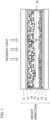
- FIG. 1 is a tandem-type photovoltaic element according to a first embodiment not representing the present invention
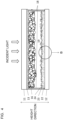
- FIG. 2 is a cross-sectional view of a tandem-type photovoltaic element according to a second embodiment not representing the present invention
- FIG. 4 is a cross-sectional view of a tandem-type photovoltaic element according to a third embodiment according to the present invention, wherein matters described below are common to FIGs. 1 , 2 and 4 , so they are described with reference to FIG. 1 as the representative drawing.
- FIGs. 1 , 2 and 4 all illustrate a tandem-type photovoltaic element comprising two photovoltaic layers, which are a first photovoltaic layer and a second photovoltaic layer.
- At least the second substrate arranged on a side from which incident light enters is composed of a transparent material, and preferably, both substrates are composed of transparent material.
- Glass is a popular transparent material, but resin, such as plastic, can be used instead of glass.
- a transparent second conductive film 13 is formed on the second substrate.
- the second conductive film 13 is preferably composed of FTO (fluorine-doped tin oxide), but other than the FTO layer, an indium-tin complex oxide (IOT) may be used, for example.
- FTO fluorine-doped tin oxide
- IOT indium-tin complex oxide
- a second photovoltaic layer 16 is formed on the second conductive film 13.
- the second photovoltaic layer 16 is composed of a substance selected from TiO 2 , SnO, ZnO, WO 3 , Nb 2 O 5 , In 2 O 3 , ZrO 2 , Ta 2 O 5 and TiSrO 3 .
- a porous titanium dioxide layer hardened by sintering is preferable.
- a composite of two or more substances described above such as a composite of SnO and ZnO or a composite of TiO 2 and Nb 2 O 5 , may also be used.
- the thickness of the second photovoltaic layer 16 in the height direction should preferably be 3-30 ⁇ m, and more preferably, 6-20 ⁇ m.
- the above-described second photovoltaic layer 16 may carry sensitized dye.
- Various dyes that exert sensitization can be applied as the dye carried by the second photovoltaic layer 16, and for example, N3 complex, N719 complex (N719 dye), Ru complex such as Ru terpyridine complex (black dye) and Ru diketonate complex, organic dyes such as coumarin dye, merocyanine dye and polyene dye, metal porphyrin dye and phthalocyanine dye are applicable.
- the Ru complex is preferable, and specifically, N719 dye and black dye are especially preferable since they exert a wide absorption spectrum in the visible light range.
- the dye can be used alone, or two or more dyes can be used in a mixture.
- a first conductive film (14 in FIGs. 1 and 2 ; 22 in FIG. 4 ) is formed on an upper surface of the first substrate 12.
- the first conductive film is preferably FTO (fluorine-doped tin oxide), but other than the FTO layer, for example, an indium - tin complex oxide (ITO) may be used.
- FTO fluorine-doped tin oxide
- ITO indium - tin complex oxide
- a charge exchange layer (15 in FIGs. 1 and 2 ; 23 in FIG. 4 ) is formed on the first conductive film.
- a platinum (Pt) film is preferable as the charge exchange layer, but carbon electrode and conductive polymer may also be used instead of the platinum (Pt) film.
- a first photovoltaic layer (21 in FIG. 1 ; 17 in FIG. 2 ; 24 in FIG. 4 ) is formed on the charge exchange layer.
- a first photovoltaic layer is composed by dispersing silicon dioxide particles 10 as a first photovoltaic layer (21 in FIG. 1 ; 17 in FIG. 2 ; 24 in FIG. 4 ) on the charge exchange layer (15 in FIGs. 1 and 2 ; 23 in FIG. 4 ).
- the silicon dioxide particles 10 that constitute the first photovoltaic layer (21 in FIG. 1 ; 17 in FIG. 2 ; 24 in FIG. 4 ) use glass particles formed for example of synthetic quartz, fused quartz glass, soda-lime glass, non-alkali glass or borosilicate glass, which are immersed in a solution of 5 - 10 % hydrofluoric acid or hydrochloric acid, washed with water and dried, and pulverized so that a major axis L of the particles is 20 to 100 nm.
- the first to third embodiments use synthetic quartz particles, which are crystalline of silicon dioxide, which are immersed in 10 % hydrofluoric solution, washed with water and dried, and pulverized so that a major axis L of the particles is 20 - 100 nm.
- Electrolyte 19 is enclosed between the first photovoltaic layer (21 in FIG. 1 ; 17 in FIG. 2 ; 24 in FIG. 4 ) and the second photovoltaic layer 16, in a space that is surrounded by a sealing member 18 on four sides.
- the electrolyte 19 is used in the prior-art dye-sensitized solar cells, and it can be of any of the following states; liquid, solid, coagulated and ordinary temperature molten salt.
- the electrolyte can be, for example, a combination of metal iodide, such as lithium iodide, sodium iodide, potassium iodide and cesium iodide, and iodine; a combination of iodine salt of quaternary ammonium compound, such as tetraalkylammonium iodide, pyridinium iodide and imidazolium iodide, and iodine; a combination of bromine compound - bromine instead of the aforementioned iodine and iodine compound; or a combination of cobalt complex.
- metal iodide such as lithium iodide, sodium iodide, potassium iodide and cesium iodide, and iodine
- a combination of iodine salt of quaternary ammonium compound such as tetraalkylammonium iodide, pyri
- the electrolyte is an ionic liquid, there is no need to use a solvent.
- the electrolyte may be a gel electrolyte, a high polymer electrolyte or a solid electrolyte, and an organic charge transport material may be used instead of the electrolyte.
- the electrolyte 19 used in the first to third embodiments is formed by adding 0.1 mol Lil, 0.05 mol I 2 , 0.5 mol 4-tetra-butylpyridine and 0.5 mol tetrabutylammonium iodide in acetonitrile solvent.
- the distance between the first photovoltaic layer (21 in FIG. 1 ; 17 in FIG. 2 ; 24 in FIG. 4 ) and the second photovoltaic layer 16 in the height direction should preferably be as short as possible, since transfer of charge becomes easier if the distance is shorter.
- the thickness of the electrolyte 19 portion in the height direction that is, the distance between the first photovoltaic layer (21 in FIG. 1 ; 17 in FIG. 2 ; 24 in FIG. 4 ) and the second photovoltaic layer 16 in the height direction, is 200 ⁇ m or smaller.
- An LED light (manufactured by Cosmotechno Co., Ltd.) was used to irradiate light from the second substrate side, and light corresponding to 1000 lux by illuminometer DT-1309 manufactured by CEM Corporation was irradiated to the photovoltaic element being the target for measurement.
- a digital multimeter was used to measure the I-V characteristics of the photovoltaic element as the target for measurement, by which values of short circuit current, open circuit voltage and form factor ff were acquired, and the maximum output value per unit area was derived.
- FIG. 1 is a view illustrating a first embodiment not representing the present invention.
- silicon dioxide particles having an average major axis L of 20 - 100 nm are used as the silicon dioxide particles 10 used in the first photovoltaic layer 21.
- These silicon dioxide particles 10 are dispersed in an overlapped manner on a flat first conductive film 14 (FTO layer) and a similarly flat charge exchange layer 15 (Pt layer) formed thereon, by which the first photovoltaic layer 21 having a thickness of 300 to 500 nm in the height direction is composed.
- FTO layer flat first conductive film 14
- Pt layer similarly flat charge exchange layer 15
- the average major axis of the silicon dioxide particles 10 is small compared to the prior art, which is considered effective in increasing the surface area of the silicon dioxide particles 10 in the first photovoltaic layer 21 and raising the photovoltaic efficiency.
- FIG. 2 is a view illustrating a second embodiment not representing the present invention.
- the second embodiment uses the same materials and the like used in the first embodiment.
- a first photovoltaic layer 17 is composed so that the silicon dioxide particles 10 are arranged on a flat first conductive film 14 and a similarly flat charge exchange layer 15 disposed thereon, so that the thickness thereof in the height direction is 300 nm or smaller.
- the thickness of the first photovoltaic layer in the height direction is reduced compared to the first embodiment.
- FIG. 3 is an enlarged view of portion A of FIG. 2 , wherein the silicon dioxide particles 10 constituting the first photovoltaic layer 17 are dispersed on the flat first conductive film 14 (FTO layer) and the similarly flat charge exchange layer 14 (Pt layer) formed thereon, in a state where there is small overlap of particles.
- FTO layer flat first conductive film 14
- Pt layer similarly flat charge exchange layer 14
- the overlapping of the silicon dioxide particles 10 in the first photovoltaic layer 17 is reduced, according to which the property of charge transfer near the first photovoltaic layer 17 is enhanced, by which the photovoltaic efficiency is considered to be increased.
- the thickness of the first photovoltaic layer 17 in the height direction should preferably be equal to or smaller than three times the average major axis L of the silicon dioxide particles.
- the silicon dioxide particles 10 should preferably be arranged on the surface of an upper layer of the charge exchange layer 15 in a dispersed manner with spaces formed therebetween. This arrangement is to prevent the silicon dioxide particles 10 from being arranged in an overcrowded manner and hindering conductivity between the charge exchange layer 15, the silicon dioxide particles 10 and the electrolyte 19. It is preferable that the charge exchange layer 15, the silicon dioxide particles 10 and the electrolyte 19 are arranged with sufficient allowance, so that the total sum of contact surface areas of the charge exchange layer 15, the silicon dioxide particles 10 and the electrolyte 19 that perform charge exchange is maximized.
- the photovoltaic amount can be increased by arranging the silicon dioxide particles 10 in the first photovoltaic layer 17 such that the charge exchange layer 15 is visible through the spaces between the silicon dioxide particles 10 when the first substrate 12 is viewed from the second substrate 11 side.
- FIG. 4 is a view illustrating a third embodiment according to the present invention.
- the third embodiment uses the same materials and the like as the first embodiment.
- a first conductive film 22 (FTO layer) and a charge exchange layer 23 (Pt layer) that constitute a base on which the silicon dioxide particles 10 are arranged are not flat.
- the first conductive film 22 has an uneven surface (roughness or asperity), with a height difference of approximately 50 nm formed on the surface.
- the charge exchange layer 23 formed on the first conductive film 22 also has a roughness on the surface, influenced by the height difference formed on the first conductive film 22.
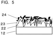
- FIG. 5 is an enlarged view of portion B of FIG. 4 .
- the silicon dioxide particles 10 constituting the first photovoltaic layer 24 are dispersed on the first conductive film 22 that has a roughness on the surface and the charge exchange layer 23 formed thereon and having a similar roughness, in a state where there is small overlap of particles.
- the arrangement of the silicon dioxide particles 10 dispersed on the charge exchange layer 23 formed on the first conductive film 22 is influenced by the surface roughness of the first conductive film 22 and charge exchange layer 23 as base layers.
- the silicon dioxide particles 10 are arranged in a thinly dispersed manner. Thereby, the silicon dioxide particles 10 are arranged with appropriate spatial allowance without excessive overlap, and therefore, the increase of photovoltaic amount is confirmed.
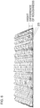
- FIG. 6 is a schematic diagram in which the first conductive film 22 is illustrated from bird's eye view.
- the shape of the surface roughness of the first conductive film 22 is not only risen steeply, as illustrated in FIG. 5 , but may also include a structure 25 where the surface is somewhat rounded, as illustrated in FIG. 6 . Further, the roughness does not have to be random, as illustrated in FIGs. 5 and 6 , and the roughness can be regularly arranged shapes, such as structural cones, trigonal pyramids, quadrangular pyramids and other pyramid shapes.
- the optimum average major axis of the silicon dioxide particles 10 may vary according to the distribution of size and shape of the silicon dioxide particles 10 constituting the first photovoltaic layer.
- the optimum value of thickness of the first conductive film in the height direction may vary according to the distribution of size and shape of the silicon dioxide particles 10.
- various optimum combinations of height difference of unevenness in the height direction of the first conductive film and/or the charge exchange layer, the shape of the roughness, and the distribution of the roughness in a direction parallel to the first substrate may be adopted in response to the distribution of size and shape of the silicon dioxide particles 10.
Landscapes
- Engineering & Computer Science (AREA)
- Power Engineering (AREA)
- Microelectronics & Electronic Packaging (AREA)
- Chemical & Material Sciences (AREA)
- Chemical Kinetics & Catalysis (AREA)
- Electrochemistry (AREA)
- Life Sciences & Earth Sciences (AREA)
- Sustainable Development (AREA)
- Materials Engineering (AREA)
- General Chemical & Material Sciences (AREA)
- Photovoltaic Devices (AREA)
- Hybrid Cells (AREA)
Description
- The present invention relates to photovoltaic elements.
- So-called solar cells and various other types of elements and devices have been devised as photovoltaic elements that convert optical energy into electric energy. The photovoltaic elements are roughly classified into two; those using silicon-based material and those using compound-based material as the material for exerting photovoltaic effect. Examples for such photovoltaic elements are published as
EP 2 421 084 A1 -
EP 2 685 554 A1 - Dye sensitized solar cells are also disclosed by: Arun Kumar D. ET AL: "Synthesis and characterization of TiO2/SiO2 nano composites for solar cell applications", Applied Nanoscience, vol. 2, no. 4, 1 December 2012 (2012-12-01), pages 429-436, XP055902829, Retrieved from the Internet: URL:https://link.springer.com/content/pdf/10.1007/s13204-012-0060-5.pdf .
- Elements that use monocrystalline silicon, polycrystalline silicon, heterojunction model, amorphous silicon and thin-film polycrystalline silicon are typical examples of elements that use silicon-based material. Meanwhile, elements using group III-V compounds, CIS (using copper (Cu), indium (In) and selenium (Se) as main components), CIGS (using copper (Cu), indium (In), gallium (Ga) and selenium (Se) as main components), CdTe, organic thin film and dye-sensitized material are examples of elements that use compound-based material.
- In addition to the above-described photovoltaic elements, there are elements using silicon dioxide, which is an insulator, as power generating material. This is based on a finding by the present inventors that silicon dioxide itself exerts photo electrolysis effect and photovoltaic effect.
- The present inventors have found that synthetic quartz and fused quartz, which are silicon dioxides, exert photovoltaic effect, and proposed a silicon dioxide solar cell as photoelectrode material and photocell material (
Patent Literatures 1 and 2). - With reference to
FIG. 7 , we will describe a tandem-type power generation element using two photovoltaic layers formed of silicon dioxide (SiO2) and titanium oxide (TiO2) as a prior art example. - In
FIG. 7 ,reference numbers - A porous
titanium dioxide layer 6 hardened by sintering is formed on theFTO layer 3 on the side from which incident light enters. The poroustitanium dioxide layer 6 carries titania particles on which are adsorbed ruthenium complex dye as sensitized dye. Further, aplatinum film 5 is formed on theFTO layer 4. - A
silicon dioxide layer 7 composed of silicon dioxide particles is formed on theplatinum film 5, so that thelayer 7 has a thickness of 0.15 - 0.20 mm in the height direction. - Moreover, the distance between the
titanium dioxide layer 6 and thesilicon dioxide layer 7 in the height direction is 0.2 mm or greater, and electrolyte 9 is sealed in a space surrounded on four sides by a sealingmember 8. - As illustrated in
FIGs. 1 ,2 ,4 and7 , the direction perpendicular to the substrate surface of the photovoltaic element is referred to as the height direction, and thickness of layers and films is described by the distance thereof. - The
silicon dioxide layer 7 serving as the photovoltaic layer is composed of silicon dioxide particles, which are formed by immersing particles of glass and the like containing silicon dioxide in a 5 - 10 % hydrofluoric solution, washing the particles with water, drying, and pulverizing the same so that the particle size is 0.2 mm or smaller. - As described, individual shapes of the pulverized silicon dioxide particles may be approximately spherical, but nonspherical particles as illustrated in
FIG. 8 also exist. - The individual
silicon dioxide particles 10 have various shapes. In the present specification, as illustrated inFIG. 8 , a maximum elongation direction of the individualsilicon dioxide particles 10 is referred to as a major axis L, and the average major axis is used to denote the shape of the silicon dioxide particles used in the photovoltaic layer and a firstphotovoltaic layer 17. In the prior art example illustrated inFIG. 7 , a material having an average major axis L of 500 - 800 nm is used. - The tandem-type photovoltaic element described here characterizes in using silicon dioxide as the photovoltaic layer. As illustrated in
FIG. 9 , it is confirmed that silicon dioxide has higher quantum efficiency than titanium dioxide even in the ultraviolet region, and that it also absorbs light in the infrared region of 2500 nm and higher. Therefore, silicon dioxide exerts photovoltaic effect in a wider wavelength region compared to titanium dioxide and realizes an extremely high power generation efficiency. According to such tandem-type photovoltaic element, the inventors of the present invention have achieved a maximum output of 28.00 µW/cm2 per unit area in an illumination of 1000 lux. -
- [PTL 1] International Publication of International Patent Application
WO 2011/049156 A1 - [PTL 2] International Publication of International Patent Application
WO 2012/124655 A1 , also published as EuropeanPatent Application EP 2 685 554 A1 - The photovoltaic elements disclosed in
PTL 1 andPTL 2,EP 2 421 084 A1 - The problem of the invention is solved by the features of
claim 1. According to one typical photovoltaic element, not forming part of the claimed invention, a photovoltaic layer of the photovoltaic element is composed of a silicon dioxide particle that has an average major axis of 100 nm or smaller. - According to another typical photovoltaic element, not forming part of the claimed invention, the photovoltaic layer of the photovoltaic element is composed of a silicon dioxide particle, and a thickness of the first photovoltaic layer in a height direction is formed to be smaller than three times the average major axis of the silicon dioxide particle.
- According to the claimed invention, a photovoltaic element is provided, said photovoltaic element comprising a first photovoltaic layer, wherein the first photovoltaic layer of the photovoltaic element is composed ofesilicon dioxide particles, and the silicon dioxide particles are arranged on a charge exchange layer that has a roughness in the height direction,
- wherein the charge exchange layer that has a roughness in a height direction is formed on an upper surface of a first conductive film that has a roughness in a height direction,
- wherein the photovoltaic element further comprises a second photovoltaic layer composed of a substance selected from TiO2 , SnO, ZnO, WO3, Nb2O5, In2O3, ZrO2, Ta2O5 and TiSrO3
- wherein the roughness of the charge exchange layer in the height direction is 50 nm or greater, and wherein the roughness of the first conductive film in the height direction is 50 nm or greater.
- The photovoltaic element described above significantly improves the power generation output per unit area compared to the prior art photovoltaic element.
- The problems, configurations and effects other than those described above will become apparent from the following description of embodiments.
-
- [
FIG. 1] FIG. 1 is a cross-sectional view of a tandem-type photovoltaic element according to a first embodiment not representing the present invention. - [
FIG. 2] FIG. 2 is a cross-sectional view of a tandem-type photovoltaic element according to a second embodiment not representing the present invention. - [
FIG. 3] FIG. 3 is an enlarged view of portion A ofFIG. 2 . - [
FIG. 4] FIG. 4 is a cross-sectional view of a tandem-type photovoltaic element according to a third embodiment according to the present invention. - [
FIG. 5] FIG. 5 is an enlarged view of portion B ofFIG. 4 . - [
FIG. 6] FIG. 6 is a schematic diagram in which a first conductive film according to the third embodiment is illustrated from bird's eye view. - [
FIG. 7] FIG. 7 is a cross-sectional view of a tandem-type photovoltaic element according to a comparative example. - [
FIG. 8] FIG. 8 is a view illustrating an example of a silicon dioxide particle. - [
FIG. 9] FIG. 9 is a measurement chart of quantum efficiency of the photovoltaic element composed of TiO2 and the photovoltaic element including SiO2 in a light wavelength region. - Now, preferred embodiments will be described with reference to the drawings. At first, matters common to the first, second and third embodiments are described.
-
FIG. 1 is a tandem-type photovoltaic element according to a first embodiment not representing the present invention,FIG. 2 is a cross-sectional view of a tandem-type photovoltaic element according to a second embodiment not representing the present invention, andFIG. 4 is a cross-sectional view of a tandem-type photovoltaic element according to a third embodiment according to the present invention, wherein matters described below are common toFIGs. 1 ,2 and4 , so they are described with reference toFIG. 1 as the representative drawing. -
FIGs. 1 ,2 and4 all illustrate a tandem-type photovoltaic element comprising two photovoltaic layers, which are a first photovoltaic layer and a second photovoltaic layer. - In
FIG. 1 , among afirst substrate 12 and asecond substrate 11, at least the second substrate arranged on a side from which incident light enters is composed of a transparent material, and preferably, both substrates are composed of transparent material. Glass is a popular transparent material, but resin, such as plastic, can be used instead of glass. - A transparent second
conductive film 13 is formed on the second substrate. The secondconductive film 13 is preferably composed of FTO (fluorine-doped tin oxide), but other than the FTO layer, an indium-tin complex oxide (IOT) may be used, for example. - A second
photovoltaic layer 16 is formed on the secondconductive film 13. The secondphotovoltaic layer 16 is composed of a substance selected from TiO2, SnO, ZnO, WO3, Nb2O5, In2O3, ZrO2, Ta2O5 and TiSrO3. A porous titanium dioxide layer hardened by sintering is preferable. - Further, a composite of two or more substances described above, such as a composite of SnO and ZnO or a composite of TiO2 and Nb2O5, may also be used.
- The thickness of the second
photovoltaic layer 16 in the height direction should preferably be 3-30 µm, and more preferably, 6-20 µm. - Further, the above-described second
photovoltaic layer 16 may carry sensitized dye. Various dyes that exert sensitization can be applied as the dye carried by the secondphotovoltaic layer 16, and for example, N3 complex, N719 complex (N719 dye), Ru complex such as Ru terpyridine complex (black dye) and Ru diketonate complex, organic dyes such as coumarin dye, merocyanine dye and polyene dye, metal porphyrin dye and phthalocyanine dye are applicable. Among these dyes, the Ru complex is preferable, and specifically, N719 dye and black dye are especially preferable since they exert a wide absorption spectrum in the visible light range. - The dye can be used alone, or two or more dyes can be used in a mixture.
- The above-described matters are common to the first, second and third embodiments and
FIGs. 1 ,2 and4 . In the following description, matters common to the first to third embodiments but have different reference numbers assigned in the drawings will be described by referring to the different reference numbers in the drawings. - A first conductive film (14 in
FIGs. 1 and2 ; 22 inFIG. 4 ) is formed on an upper surface of thefirst substrate 12. The first conductive film is preferably FTO (fluorine-doped tin oxide), but other than the FTO layer, for example, an indium - tin complex oxide (ITO) may be used. - A charge exchange layer (15 in
FIGs. 1 and2 ; 23 inFIG. 4 ) is formed on the first conductive film. A platinum (Pt) film is preferable as the charge exchange layer, but carbon electrode and conductive polymer may also be used instead of the platinum (Pt) film. - A first photovoltaic layer (21 in
FIG. 1 ; 17 inFIG. 2 ; 24 inFIG. 4 ) is formed on the charge exchange layer. - In any of the first to third embodiments, a first photovoltaic layer is composed by dispersing
silicon dioxide particles 10 as a first photovoltaic layer (21 inFIG. 1 ; 17 inFIG. 2 ; 24 inFIG. 4 ) on the charge exchange layer (15 inFIGs. 1 and2 ; 23 inFIG. 4 ). - The
silicon dioxide particles 10 that constitute the first photovoltaic layer (21 inFIG. 1 ; 17 inFIG. 2 ; 24 inFIG. 4 ) use glass particles formed for example of synthetic quartz, fused quartz glass, soda-lime glass, non-alkali glass or borosilicate glass, which are immersed in a solution of 5 - 10 % hydrofluoric acid or hydrochloric acid, washed with water and dried, and pulverized so that a major axis L of the particles is 20 to 100 nm. The first to third embodiments use synthetic quartz particles, which are crystalline of silicon dioxide, which are immersed in 10 % hydrofluoric solution, washed with water and dried, and pulverized so that a major axis L of the particles is 20 - 100 nm. -
Electrolyte 19 is enclosed between the first photovoltaic layer (21 inFIG. 1 ; 17 inFIG. 2 ; 24 inFIG. 4 ) and the secondphotovoltaic layer 16, in a space that is surrounded by a sealingmember 18 on four sides. Theelectrolyte 19 is used in the prior-art dye-sensitized solar cells, and it can be of any of the following states; liquid, solid, coagulated and ordinary temperature molten salt. - The electrolyte can be, for example, a combination of metal iodide, such as lithium iodide, sodium iodide, potassium iodide and cesium iodide, and iodine; a combination of iodine salt of quaternary ammonium compound, such as tetraalkylammonium iodide, pyridinium iodide and imidazolium iodide, and iodine; a combination of bromine compound - bromine instead of the aforementioned iodine and iodine compound; or a combination of cobalt complex.
- If the electrolyte is an ionic liquid, there is no need to use a solvent. The electrolyte may be a gel electrolyte, a high polymer electrolyte or a solid electrolyte, and an organic charge transport material may be used instead of the electrolyte.
- If the
electrolyte 19 is in a state of a solution, the solvent may be, for example, nitrile-based solvent such as acetonitrile, metoxyacetonitrile and propionitrile, carbonate-based solvent such as ethylene carbonate, and ether-based solvent. - Specifically, the
electrolyte 19 used in the first to third embodiments is formed by adding 0.1 mol Lil, 0.05 mol I2, 0.5 mol 4-tetra-butylpyridine and 0.5 mol tetrabutylammonium iodide in acetonitrile solvent. - The distance between the first photovoltaic layer (21 in
FIG. 1 ; 17 inFIG. 2 ; 24 inFIG. 4 ) and the secondphotovoltaic layer 16 in the height direction should preferably be as short as possible, since transfer of charge becomes easier if the distance is shorter. - In the first to third embodiments, the thickness of the
electrolyte 19 portion in the height direction, that is, the distance between the first photovoltaic layer (21 inFIG. 1 ; 17 inFIG. 2 ; 24 inFIG. 4 ) and the secondphotovoltaic layer 16 in the height direction, is 200 µm or smaller. - Method for evaluating the maximum output value per unit area according to the present specification is as described below.
- An LED light (manufactured by Cosmotechno Co., Ltd.) was used to irradiate light from the second substrate side, and light corresponding to 1000 lux by illuminometer DT-1309 manufactured by CEM Corporation was irradiated to the photovoltaic element being the target for measurement. A digital multimeter was used to measure the I-V characteristics of the photovoltaic element as the target for measurement, by which values of short circuit current, open circuit voltage and form factor ff were acquired, and the maximum output value per unit area was derived.
- Hereafter, characteristics of the present embodiments will be described with reference to the drawings. The other portions are similar to the description regarding the matters common to the first to third embodiments described above.
-
FIG. 1 is a view illustrating a first embodiment not representing the present invention. In the first embodiment, silicon dioxide particles having an average major axis L of 20 - 100 nm are used as thesilicon dioxide particles 10 used in the firstphotovoltaic layer 21. Thesesilicon dioxide particles 10 are dispersed in an overlapped manner on a flat first conductive film 14 (FTO layer) and a similarly flat charge exchange layer 15 (Pt layer) formed thereon, by which the firstphotovoltaic layer 21 having a thickness of 300 to 500 nm in the height direction is composed. - Other conditions are as described as matters common to the first to third embodiments.
- As a result, the embodiment realizes a significant improvement of photovoltaic efficiency compared to the prior art example described in the background art.
L t FTO layer roughness Maximum output per unit area Prior Art 500~800nm 0.15~0.20mm Very little surface height difference 28.00µW/cm2 First Embodiment 20~100nm 300-500nm Very little surface height difference 35.00µW/cm2 L: Average major axis of silicon dioxide particles
t: Silicon dioxide layer thickness - In the first embodiment, the average major axis of the
silicon dioxide particles 10 is small compared to the prior art, which is considered effective in increasing the surface area of thesilicon dioxide particles 10 in the firstphotovoltaic layer 21 and raising the photovoltaic efficiency. -
FIG. 2 is a view illustrating a second embodiment not representing the present invention. The second embodiment uses the same materials and the like used in the first embodiment. However, in the second embodiment, a firstphotovoltaic layer 17 is composed so that thesilicon dioxide particles 10 are arranged on a flat firstconductive film 14 and a similarly flatcharge exchange layer 15 disposed thereon, so that the thickness thereof in the height direction is 300 nm or smaller. - That is, the thickness of the first photovoltaic layer in the height direction is reduced compared to the first embodiment.
-
FIG. 3 is an enlarged view of portion A ofFIG. 2 , wherein thesilicon dioxide particles 10 constituting the firstphotovoltaic layer 17 are dispersed on the flat first conductive film 14 (FTO layer) and the similarly flat charge exchange layer 14 (Pt layer) formed thereon, in a state where there is small overlap of particles. - As a result, the embodiment realizes a significant improvement of photovoltaic efficiency compared to the prior art example described in the background art.
L t FTO layer roughness Maximum output per unit area Prior Art 500~800nm 0.15~0.20mm Very little surface height difference 28.00µW/cm2 Second Embodiment 20~100nm 300nm or less Very little surface height difference 45.48µW/cm2 L: Average major axis of silicon dioxide particles
t: Silicon dioxide layer thickness - In the second embodiment, the overlapping of the
silicon dioxide particles 10 in the firstphotovoltaic layer 17 is reduced, according to which the property of charge transfer near the firstphotovoltaic layer 17 is enhanced, by which the photovoltaic efficiency is considered to be increased. - Therefore, it is important not to arrange too much
silicon dioxide particles 10 on the upper surface of thecharge exchange layer 15 in order to improve the photovoltaic efficiency. That is, it has been confirmed that the photovoltaic amount is increased if thesilicon dioxide particles 10 are not excessively overlapped and sufficient space is formed therebetween. - Therefore, the thickness of the first
photovoltaic layer 17 in the height direction should preferably be equal to or smaller than three times the average major axis L of the silicon dioxide particles. - The
silicon dioxide particles 10 should preferably be arranged on the surface of an upper layer of thecharge exchange layer 15 in a dispersed manner with spaces formed therebetween. This arrangement is to prevent thesilicon dioxide particles 10 from being arranged in an overcrowded manner and hindering conductivity between thecharge exchange layer 15, thesilicon dioxide particles 10 and theelectrolyte 19. It is preferable that thecharge exchange layer 15, thesilicon dioxide particles 10 and theelectrolyte 19 are arranged with sufficient allowance, so that the total sum of contact surface areas of thecharge exchange layer 15, thesilicon dioxide particles 10 and theelectrolyte 19 that perform charge exchange is maximized. - Therefore, the photovoltaic amount can be increased by arranging the
silicon dioxide particles 10 in the firstphotovoltaic layer 17 such that thecharge exchange layer 15 is visible through the spaces between thesilicon dioxide particles 10 when thefirst substrate 12 is viewed from thesecond substrate 11 side. -
FIG. 4 is a view illustrating a third embodiment according to the present invention. The third embodiment uses the same materials and the like as the first embodiment. However, in the third embodiment, a first conductive film 22 (FTO layer) and a charge exchange layer 23 (Pt layer) that constitute a base on which thesilicon dioxide particles 10 are arranged are not flat. As illustrated inFIG. 4 , the first conductive film 22 has an uneven surface (roughness or asperity), with a height difference of approximately 50 nm formed on the surface. Thecharge exchange layer 23 formed on the first conductive film 22 also has a roughness on the surface, influenced by the height difference formed on the first conductive film 22. -
FIG. 5 is an enlarged view of portion B ofFIG. 4 . Thesilicon dioxide particles 10 constituting the firstphotovoltaic layer 24 are dispersed on the first conductive film 22 that has a roughness on the surface and thecharge exchange layer 23 formed thereon and having a similar roughness, in a state where there is small overlap of particles. - The difference of height of the surface roughness of the first conductive film 22 should be 50 nm or greater, and more preferably, 100 nm or greater. Further, it is preferable that the
charge exchange layer 23 formed on the first conductive film 22 is formed in a manner maintaining the shape of the roughness on the surface of the first conductive film 22 without burying the surface roughness of the first conductive film 22. - As a result, the embodiment realizes an even further significant improvement of photovoltaic efficiency compared to the prior art example described in the background art.
L t FTO layer roughness Maximum output per unit area Prior Art 500~800nm 0.15~0.20mm Very little surface height difference 28.00µW/cm2 Third Embodiment 20-100nm 300nm or less Surface height difference approx. 50 nm 70.8µW/cm2 L: Average major axis of silicon dioxide particles
t: Silicon dioxide layer thickness - The arrangement of the
silicon dioxide particles 10 dispersed on thecharge exchange layer 23 formed on the first conductive film 22 is influenced by the surface roughness of the first conductive film 22 andcharge exchange layer 23 as base layers. - Thanks to the surface roughness of the base layers, the
silicon dioxide particles 10 are arranged in a thinly dispersed manner. Thereby, thesilicon dioxide particles 10 are arranged with appropriate spatial allowance without excessive overlap, and therefore, the increase of photovoltaic amount is confirmed. -
FIG. 6 is a schematic diagram in which the first conductive film 22 is illustrated from bird's eye view. The shape of the surface roughness of the first conductive film 22 is not only risen steeply, as illustrated inFIG. 5 , but may also include astructure 25 where the surface is somewhat rounded, as illustrated inFIG. 6 . Further, the roughness does not have to be random, as illustrated inFIGs. 5 and6 , and the roughness can be regularly arranged shapes, such as structural cones, trigonal pyramids, quadrangular pyramids and other pyramid shapes. - In the first to third embodiments, various modifications are possible. For example, the optimum average major axis of the
silicon dioxide particles 10 may vary according to the distribution of size and shape of thesilicon dioxide particles 10 constituting the first photovoltaic layer. Similarly, the optimum value of thickness of the first conductive film in the height direction may vary according to the distribution of size and shape of thesilicon dioxide particles 10. - Further, various optimum combinations of height difference of unevenness in the height direction of the first conductive film and/or the charge exchange layer, the shape of the roughness, and the distribution of the roughness in a direction parallel to the first substrate may be adopted in response to the distribution of size and shape of the
silicon dioxide particles 10. -
- 10
- silicon dioxide particle
- 11
- second substrate
- 12
- first substrate
- 13
- second conductive film
- 14
- first conductive film
- 15
- charge exchange layer
- 16
- second photovoltaic layer
- 17
- first photovoltaic layer
- 18
- sealing member
- 19
- electrolyte
- 21
- first photovoltaic layer
- 22
- first conductive film
- 23
- charge exchange layer
- 24
- first photovoltaic layer
Claims (4)
- A photovoltaic element comprising a first photovoltaic layer (24),wherein the first photovoltaic layer (24) is composed of silicon dioxide particles (10), andthe silicon dioxide particles (10) are arranged on a charge exchange layer (23) that has a roughness in a height direction,wherein the charge exchange layer (23) that has a roughness in a height direction is formed on an upper surface of a first conductive film (22) that has a roughness in a height direction,wherein the photovoltaic element further comprises a second photovoltaic layer (16) composed of a substance selected from TiO2, SnO, ZnO, WO3, Nb2O5, In2O3, ZrO2, Ta2O5 and TiSrO3whereinthe roughness of the charge exchange layer (23) in the height direction is 50 nm or greater, and characterized in thatthe roughness of the first conductive film (22) in the height direction is 50 nm or greater.
- The photovoltaic element according to claim 1, further comprising:a first substrate (12) comprising the first conductive film (22) on one surface and a second substrate (11) comprising a second conductive film (13) on one surface are arranged such that the first conductive film (22) and the second conductive film (13) face each other;wherein the second photovoltaic layer (16) is arranged on the second conductive film (13);wherein the charge exchange layer (23) is arranged on the first conductive film (22);the first photovoltaic layer (24) is arranged on the charge exchange layer (23); andan electrolyte (19) is arranged between the second photovoltaic layer (16) and the first photovoltaic layer (24).
- The photovoltaic element according to any one of claims 1 or 2,
wherein the silicon dioxide particle (10) is silicon dioxide immersed in hydrogen halide. - The photovoltaic element according to any one of claims 1 to 3,
wherein the second photovoltaic layer (16) comprises sensitized dye carried thereon.
Applications Claiming Priority (3)
| Application Number | Priority Date | Filing Date | Title |
|---|---|---|---|
| JP2016001278A JP6773944B2 (en) | 2016-01-06 | 2016-01-06 | Photovoltaic element |
| EP16883856.3A EP3401938B1 (en) | 2016-01-06 | 2016-12-27 | Photovoltaic element |
| PCT/JP2016/088848 WO2017119357A1 (en) | 2016-01-06 | 2016-12-27 | Photovoltaic element |
Related Parent Applications (2)
| Application Number | Title | Priority Date | Filing Date |
|---|---|---|---|
| EP16883856.3A Division EP3401938B1 (en) | 2016-01-06 | 2016-12-27 | Photovoltaic element |
| EP16883856.3A Division-Into EP3401938B1 (en) | 2016-01-06 | 2016-12-27 | Photovoltaic element |
Publications (2)
| Publication Number | Publication Date |
|---|---|
| EP3758032A1 EP3758032A1 (en) | 2020-12-30 |
| EP3758032B1 true EP3758032B1 (en) | 2025-05-14 |
Family
ID=59274092
Family Applications (2)
| Application Number | Title | Priority Date | Filing Date |
|---|---|---|---|
| EP16883856.3A Active EP3401938B1 (en) | 2016-01-06 | 2016-12-27 | Photovoltaic element |
| EP20191884.4A Active EP3758032B1 (en) | 2016-01-06 | 2016-12-27 | Photovoltaic element |
Family Applications Before (1)
| Application Number | Title | Priority Date | Filing Date |
|---|---|---|---|
| EP16883856.3A Active EP3401938B1 (en) | 2016-01-06 | 2016-12-27 | Photovoltaic element |
Country Status (13)
| Country | Link |
|---|---|
| US (2) | US20190006121A1 (en) |
| EP (2) | EP3401938B1 (en) |
| JP (1) | JP6773944B2 (en) |
| CN (2) | CN108475582B (en) |
| AU (2) | AU2016385211B2 (en) |
| DK (2) | DK3758032T3 (en) |
| ES (2) | ES3030687T3 (en) |
| FI (1) | FI3758032T3 (en) |
| PH (1) | PH12018501441A1 (en) |
| PL (2) | PL3401938T3 (en) |
| RU (1) | RU2703519C1 (en) |
| TW (1) | TWI708274B (en) |
| WO (1) | WO2017119357A1 (en) |
Families Citing this family (2)
| Publication number | Priority date | Publication date | Assignee | Title |
|---|---|---|---|---|
| JP2019021767A (en) * | 2017-07-18 | 2019-02-07 | 国際先端技術総合研究所株式会社 | Optical power generation element and manufacturing method thereof |
| RU196426U1 (en) * | 2019-12-27 | 2020-02-28 | федеральное государственное автономное образовательное учреждение высшего образования "Национальный исследовательский университет ИТМО" (Университет ИТМО) | Oxide transparent heterojunction |
Family Cites Families (29)
| Publication number | Priority date | Publication date | Assignee | Title |
|---|---|---|---|---|
| JPH11317538A (en) * | 1998-02-17 | 1999-11-16 | Canon Inc | Photoconductive thin film and photovoltaic element |
| FR2800731B1 (en) * | 1999-11-05 | 2002-01-18 | Saint Gobain Vitrage | TRANSPARENT SUBSTRATE HAVING A SILICON-DERIVED LAYER |
| EP1180774B1 (en) * | 2000-08-15 | 2006-10-11 | Fuji Photo Film Co., Ltd. | Photoelectric conversion device and method for producing same |
| JP2005111218A (en) * | 2003-10-07 | 2005-04-28 | Rabaa:Kk | Clothes storing wash net |
| WO2005078853A1 (en) * | 2004-02-13 | 2005-08-25 | Bridgestone Corporation | Dye-sensitized solar cell |
| JP4863662B2 (en) * | 2005-07-06 | 2012-01-25 | シャープ株式会社 | Dye-sensitized solar cell module and manufacturing method thereof |
| JP4856079B2 (en) * | 2005-09-02 | 2012-01-18 | 京セラ株式会社 | PHOTOELECTRIC CONVERSION DEVICE, MANUFACTURING METHOD THEREOF, AND PHOTOVOLTAIC GENERATION DEVICE |
| WO2007043533A1 (en) * | 2005-10-11 | 2007-04-19 | Kyocera Corporation | Photoelectric transducer, process for producing the same, and photovoltaic apparatus |
| KR100728194B1 (en) * | 2005-11-11 | 2007-06-13 | 삼성에스디아이 주식회사 | Dye-sensitized solar cell and method for producing same |
| US7902072B2 (en) * | 2006-02-28 | 2011-03-08 | Fujifilm Corporation | Metal-polishing composition and chemical-mechanical polishing method |
| EP1936644A3 (en) * | 2006-12-22 | 2011-01-05 | Sony Deutschland Gmbh | A photovoltaic cell |
| JP2008257893A (en) * | 2007-03-30 | 2008-10-23 | Dainippon Printing Co Ltd | A method for producing a dye-sensitized solar cell substrate, a method for producing a dye-sensitized solar cell, and a dye-sensitized solar cell substrate and a dye-sensitized solar cell produced thereby. |
| CN102027556B (en) * | 2008-04-18 | 2013-04-17 | Nlab太阳能股份公司 | Solar-to-electric energy conversion device |
| CN101620938B (en) * | 2008-07-05 | 2011-12-14 | 比亚迪股份有限公司 | Semiconductor electrode, preparation method thereof and solar cell comprising semiconductor electrode |
| WO2010046180A2 (en) * | 2008-10-22 | 2010-04-29 | Applied Materials Inc. - A Corporation Of The State Of Delaware | Semiconductor device and method of producing a semiconductor device |
| JP5422645B2 (en) * | 2009-04-15 | 2014-02-19 | シャープ株式会社 | Dye-sensitized solar cell and dye-sensitized solar cell module |
| CN101866963B (en) * | 2009-07-20 | 2012-12-26 | 湖南共创光伏科技有限公司 | Silicon-based multijunction multi-laminated PIN thin film solar cell with high conversion rate and production method thereof |
| AU2010308884A1 (en) | 2009-10-21 | 2012-05-10 | International Frontier Technology Laboratory, Inc. | Photoelectrode material and photocell material |
| US9224892B2 (en) * | 2009-12-21 | 2015-12-29 | Ppg Industries Ohio, Inc. | Silicon thin film solar cell having improved haze and methods of making the same |
| KR101135476B1 (en) * | 2010-11-16 | 2012-04-13 | 삼성에스디아이 주식회사 | Dye-sensitized solar cell |
| TWI542023B (en) | 2011-03-11 | 2016-07-11 | Internat Frontier Tech Lab Inc | Silicon dioxide solar cells |
| JP2012234693A (en) * | 2011-04-28 | 2012-11-29 | International Frontier Technology Laboratory Inc | Solar cell |
| JP5118233B2 (en) * | 2011-06-08 | 2013-01-16 | シャープ株式会社 | Photoelectric conversion element and photoelectric conversion element module |
| CN102543468A (en) * | 2012-01-04 | 2012-07-04 | 复旦大学 | Dye-sensitized solar cell with oriented carbon nanotube thin film as counter electrode |
| JP5467237B2 (en) * | 2012-02-09 | 2014-04-09 | ペクセル・テクノロジーズ株式会社 | Dye-sensitized photoelectric conversion device and method for producing dye-sensitized solar cell using the same |
| CN102751105B (en) * | 2012-06-26 | 2015-07-15 | 北京交通大学 | Preparation method of dye-sensitized solar cell photoanode |
| JP2014095099A (en) * | 2012-11-07 | 2014-05-22 | Sumitomo Metal Mining Co Ltd | Transparent conductive film laminate, method of producing transparent conductive film laminate, thin-film solar cell and method of producing thin-film solar cell |
| JP6235235B2 (en) * | 2013-05-10 | 2017-11-22 | 三愛工業株式会社 | Laundry net bag |
| JP6121971B2 (en) * | 2014-10-17 | 2017-04-26 | 松本ナ−ス産業株式会社 | Laundry net |
-
2016
- 2016-01-06 JP JP2016001278A patent/JP6773944B2/en active Active
- 2016-12-27 DK DK20191884.4T patent/DK3758032T3/en active
- 2016-12-27 ES ES20191884T patent/ES3030687T3/en active Active
- 2016-12-27 PL PL16883856T patent/PL3401938T3/en unknown
- 2016-12-27 PL PL20191884.4T patent/PL3758032T3/en unknown
- 2016-12-27 DK DK16883856.3T patent/DK3401938T3/en active
- 2016-12-27 AU AU2016385211A patent/AU2016385211B2/en active Active
- 2016-12-27 RU RU2018127840A patent/RU2703519C1/en active
- 2016-12-27 ES ES16883856T patent/ES2910044T3/en active Active
- 2016-12-27 CN CN201680077860.2A patent/CN108475582B/en active Active
- 2016-12-27 US US16/067,988 patent/US20190006121A1/en not_active Abandoned
- 2016-12-27 EP EP16883856.3A patent/EP3401938B1/en active Active
- 2016-12-27 EP EP20191884.4A patent/EP3758032B1/en active Active
- 2016-12-27 CN CN202010156599.3A patent/CN111508715A/en active Pending
- 2016-12-27 FI FIEP20191884.4T patent/FI3758032T3/en active
- 2016-12-27 WO PCT/JP2016/088848 patent/WO2017119357A1/en not_active Ceased
- 2016-12-29 TW TW105143927A patent/TWI708274B/en active
-
2018
- 2018-07-05 PH PH12018501441A patent/PH12018501441A1/en unknown
-
2019
- 2019-08-21 AU AU2019219769A patent/AU2019219769B2/en active Active
-
2020
- 2020-04-29 US US16/861,398 patent/US20200279694A1/en not_active Abandoned
Non-Patent Citations (1)
| Title |
|---|
| ARUN KUMAR D. ET AL: "Synthesis and characterization of TiO2/SiO2 nano composites for solar cell applications", APPLIED NANOSCIENCE, vol. 2, no. 4, 1 December 2012 (2012-12-01), pages 429 - 436, XP055902829, ISSN: 2190-5509, Retrieved from the Internet <URL:https://link.springer.com/content/pdf/10.1007/s13204-012-0060-5.pdf> DOI: 10.1007/s13204-012-0060-5 * |
Also Published As
| Publication number | Publication date |
|---|---|
| CN111508715A (en) | 2020-08-07 |
| EP3758032A1 (en) | 2020-12-30 |
| PH12018501441A1 (en) | 2019-03-04 |
| AU2016385211B2 (en) | 2019-10-03 |
| AU2019219769B2 (en) | 2021-01-21 |
| CN108475582B (en) | 2021-02-23 |
| PL3758032T3 (en) | 2025-07-28 |
| US20190006121A1 (en) | 2019-01-03 |
| EP3401938B1 (en) | 2022-01-19 |
| DK3758032T3 (en) | 2025-05-19 |
| TW201801109A (en) | 2018-01-01 |
| PL3401938T3 (en) | 2022-05-23 |
| ES2910044T3 (en) | 2022-05-11 |
| AU2016385211A1 (en) | 2018-07-26 |
| WO2017119357A1 (en) | 2017-07-13 |
| JP6773944B2 (en) | 2020-10-21 |
| DK3401938T3 (en) | 2022-03-28 |
| EP3401938A4 (en) | 2020-01-08 |
| TWI708274B (en) | 2020-10-21 |
| JP2017123392A (en) | 2017-07-13 |
| RU2703519C1 (en) | 2019-10-18 |
| FI3758032T3 (en) | 2025-07-08 |
| EP3401938A1 (en) | 2018-11-14 |
| CN108475582A (en) | 2018-08-31 |
| US20200279694A1 (en) | 2020-09-03 |
| ES3030687T3 (en) | 2025-07-01 |
| AU2019219769A1 (en) | 2019-09-05 |
Similar Documents
| Publication | Publication Date | Title |
|---|---|---|
| US9805878B2 (en) | Silicon dioxide solar cell | |
| CN102522506A (en) | Organic solar cell of suede light trapping electrode and manufacturing method thereof | |
| JP5586489B2 (en) | Electrode substrate for dye-sensitive solar cell and dye-sensitive solar cell comprising the same | |
| Bhambhani | Quantum dot-sensitized solar cells: a review | |
| EP3758032B1 (en) | Photovoltaic element | |
| CN103426645B (en) | Utilize metal flexible DSSC and the manufacture method thereof of the metal substrate of dual coating | |
| KR101447618B1 (en) | Light sensitized Solar Cell and Method for manufacturing the same | |
| CN103578775B (en) | Dye-sensitized solar cell based on ZnO transparent conductive nanowire array electrode and its preparation method | |
| HK40000196A (en) | Photovoltaic element | |
| KR100670331B1 (en) | Plastic electrode and solar cell using same | |
| Shaban et al. | Efficiency Performance Effect of TiO 2 Thickness Deposited on FTO Coated Glass Photoanode | |
| Zheng et al. | The research of CaO/TiO 2 nanocrystalline film for dye-sensitized solar cell | |
| JP6670430B2 (en) | Photovoltaic element and method of manufacturing photovoltaic element | |
| KR101477037B1 (en) | Metal flexible dye-sensitized solar cell with texturing azo glass transparent electrode and double coating metal substrate and manufacturing method thereof | |
| Hieu et al. | Enhancement of dye-sensitized solar cell efficiency by spherical voids in nanocrystalline ZnO electrodes | |
| RO137627A2 (en) | Dye-photosensitized solar cells | |
| KR101215313B1 (en) | Metal flexible dye-sensitized solar cell with coating metal substrate and manufacturing method thereof | |
| TWM486145U (en) | Dye-sensitized solar cell |
Legal Events
| Date | Code | Title | Description |
|---|---|---|---|
| PUAI | Public reference made under article 153(3) epc to a published international application that has entered the european phase |
Free format text: ORIGINAL CODE: 0009012 |
|
| STAA | Information on the status of an ep patent application or granted ep patent |
Free format text: STATUS: REQUEST FOR EXAMINATION WAS MADE |
|
| 17P | Request for examination filed |
Effective date: 20200820 |
|
| AC | Divisional application: reference to earlier application |
Ref document number: 3401938 Country of ref document: EP Kind code of ref document: P |
|
| AK | Designated contracting states |
Kind code of ref document: A1 Designated state(s): AL AT BE BG CH CY CZ DE DK EE ES FI FR GB GR HR HU IE IS IT LI LT LU LV MC MK MT NL NO PL PT RO RS SE SI SK SM TR |
|
| STAA | Information on the status of an ep patent application or granted ep patent |
Free format text: STATUS: EXAMINATION IS IN PROGRESS |
|
| 17Q | First examination report despatched |
Effective date: 20220404 |
|
| GRAP | Despatch of communication of intention to grant a patent |
Free format text: ORIGINAL CODE: EPIDOSNIGR1 |
|
| STAA | Information on the status of an ep patent application or granted ep patent |
Free format text: STATUS: GRANT OF PATENT IS INTENDED |
|
| INTG | Intention to grant announced |
Effective date: 20241213 |
|
| GRAS | Grant fee paid |
Free format text: ORIGINAL CODE: EPIDOSNIGR3 |
|
| GRAA | (expected) grant |
Free format text: ORIGINAL CODE: 0009210 |
|
| STAA | Information on the status of an ep patent application or granted ep patent |
Free format text: STATUS: THE PATENT HAS BEEN GRANTED |
|
| AC | Divisional application: reference to earlier application |
Ref document number: 3401938 Country of ref document: EP Kind code of ref document: P |
|
| AK | Designated contracting states |
Kind code of ref document: B1 Designated state(s): AL AT BE BG CH CY CZ DE DK EE ES FI FR GB GR HR HU IE IS IT LI LT LU LV MC MK MT NL NO PL PT RO RS SE SI SK SM TR |
|
| REG | Reference to a national code |
Ref country code: GB Ref legal event code: FG4D |
|
| REG | Reference to a national code |
Ref country code: CH Ref legal event code: EP |
|
| REG | Reference to a national code |
Ref country code: DK Ref legal event code: T3 Effective date: 20250516 |
|
| REG | Reference to a national code |
Ref country code: DE Ref legal event code: R096 Ref document number: 602016092276 Country of ref document: DE |
|
| REG | Reference to a national code |
Ref country code: NL Ref legal event code: FP Ref country code: IE Ref legal event code: FG4D |
|
| REG | Reference to a national code |
Ref country code: SE Ref legal event code: TRGR |
|
| REG | Reference to a national code |
Ref country code: ES Ref legal event code: FG2A Ref document number: 3030687 Country of ref document: ES Kind code of ref document: T3 Effective date: 20250701 |
|
| REG | Reference to a national code |
Ref country code: FI Ref legal event code: FGE |
|
| PG25 | Lapsed in a contracting state [announced via postgrant information from national office to epo] |
Ref country code: PT Free format text: LAPSE BECAUSE OF FAILURE TO SUBMIT A TRANSLATION OF THE DESCRIPTION OR TO PAY THE FEE WITHIN THE PRESCRIBED TIME-LIMIT Effective date: 20250915 |
|
| REG | Reference to a national code |
Ref country code: LT Ref legal event code: MG9D |
|
| PG25 | Lapsed in a contracting state [announced via postgrant information from national office to epo] |
Ref country code: GR Free format text: LAPSE BECAUSE OF FAILURE TO SUBMIT A TRANSLATION OF THE DESCRIPTION OR TO PAY THE FEE WITHIN THE PRESCRIBED TIME-LIMIT Effective date: 20250815 |
|
| REG | Reference to a national code |
Ref country code: AT Ref legal event code: MK05 Ref document number: 1795549 Country of ref document: AT Kind code of ref document: T Effective date: 20250514 |
|
| PG25 | Lapsed in a contracting state [announced via postgrant information from national office to epo] |
Ref country code: BG Free format text: LAPSE BECAUSE OF FAILURE TO SUBMIT A TRANSLATION OF THE DESCRIPTION OR TO PAY THE FEE WITHIN THE PRESCRIBED TIME-LIMIT Effective date: 20250514 |
|
| PG25 | Lapsed in a contracting state [announced via postgrant information from national office to epo] |
Ref country code: HR Free format text: LAPSE BECAUSE OF FAILURE TO SUBMIT A TRANSLATION OF THE DESCRIPTION OR TO PAY THE FEE WITHIN THE PRESCRIBED TIME-LIMIT Effective date: 20250514 |
|
| PG25 | Lapsed in a contracting state [announced via postgrant information from national office to epo] |
Ref country code: AT Free format text: LAPSE BECAUSE OF FAILURE TO SUBMIT A TRANSLATION OF THE DESCRIPTION OR TO PAY THE FEE WITHIN THE PRESCRIBED TIME-LIMIT Effective date: 20250514 |
|
| PG25 | Lapsed in a contracting state [announced via postgrant information from national office to epo] |
Ref country code: RS Free format text: LAPSE BECAUSE OF FAILURE TO SUBMIT A TRANSLATION OF THE DESCRIPTION OR TO PAY THE FEE WITHIN THE PRESCRIBED TIME-LIMIT Effective date: 20250814 |
|
| PG25 | Lapsed in a contracting state [announced via postgrant information from national office to epo] |
Ref country code: IS Free format text: LAPSE BECAUSE OF FAILURE TO SUBMIT A TRANSLATION OF THE DESCRIPTION OR TO PAY THE FEE WITHIN THE PRESCRIBED TIME-LIMIT Effective date: 20250914 |
|
| PG25 | Lapsed in a contracting state [announced via postgrant information from national office to epo] |
Ref country code: LV Free format text: LAPSE BECAUSE OF FAILURE TO SUBMIT A TRANSLATION OF THE DESCRIPTION OR TO PAY THE FEE WITHIN THE PRESCRIBED TIME-LIMIT Effective date: 20250514 |
|
| PGFP | Annual fee paid to national office [announced via postgrant information from national office to epo] |
Ref country code: NL Payment date: 20251126 Year of fee payment: 10 |
|
| REG | Reference to a national code |
Ref country code: CH Ref legal event code: U11 Free format text: ST27 STATUS EVENT CODE: U-0-0-U10-U11 (AS PROVIDED BY THE NATIONAL OFFICE) Effective date: 20260101 |
|
| PGFP | Annual fee paid to national office [announced via postgrant information from national office to epo] |
Ref country code: DE Payment date: 20251119 Year of fee payment: 10 |
|
| PGFP | Annual fee paid to national office [announced via postgrant information from national office to epo] |
Ref country code: GB Payment date: 20251113 Year of fee payment: 10 |
|
| PGFP | Annual fee paid to national office [announced via postgrant information from national office to epo] |
Ref country code: NO Payment date: 20251210 Year of fee payment: 10 |
|
| PG25 | Lapsed in a contracting state [announced via postgrant information from national office to epo] |
Ref country code: SM Free format text: LAPSE BECAUSE OF FAILURE TO SUBMIT A TRANSLATION OF THE DESCRIPTION OR TO PAY THE FEE WITHIN THE PRESCRIBED TIME-LIMIT Effective date: 20250514 |
|
| PGFP | Annual fee paid to national office [announced via postgrant information from national office to epo] |
Ref country code: IT Payment date: 20251126 Year of fee payment: 10 Ref country code: FI Payment date: 20251211 Year of fee payment: 10 Ref country code: DK Payment date: 20251212 Year of fee payment: 10 |
|
| PGFP | Annual fee paid to national office [announced via postgrant information from national office to epo] |
Ref country code: FR Payment date: 20251124 Year of fee payment: 10 |
|
| PGFP | Annual fee paid to national office [announced via postgrant information from national office to epo] |
Ref country code: SE Payment date: 20251126 Year of fee payment: 10 |
|
| PG25 | Lapsed in a contracting state [announced via postgrant information from national office to epo] |
Ref country code: CZ Free format text: LAPSE BECAUSE OF FAILURE TO SUBMIT A TRANSLATION OF THE DESCRIPTION OR TO PAY THE FEE WITHIN THE PRESCRIBED TIME-LIMIT Effective date: 20250514 |
|
| PGFP | Annual fee paid to national office [announced via postgrant information from national office to epo] |
Ref country code: IE Payment date: 20251126 Year of fee payment: 10 |
|
| PGFP | Annual fee paid to national office [announced via postgrant information from national office to epo] |
Ref country code: PL Payment date: 20251215 Year of fee payment: 10 |
|
| PG25 | Lapsed in a contracting state [announced via postgrant information from national office to epo] |
Ref country code: EE Free format text: LAPSE BECAUSE OF FAILURE TO SUBMIT A TRANSLATION OF THE DESCRIPTION OR TO PAY THE FEE WITHIN THE PRESCRIBED TIME-LIMIT Effective date: 20250514 |
|
| PG25 | Lapsed in a contracting state [announced via postgrant information from national office to epo] |
Ref country code: RO Free format text: LAPSE BECAUSE OF FAILURE TO SUBMIT A TRANSLATION OF THE DESCRIPTION OR TO PAY THE FEE WITHIN THE PRESCRIBED TIME-LIMIT Effective date: 20250514 Ref country code: SK Free format text: LAPSE BECAUSE OF FAILURE TO SUBMIT A TRANSLATION OF THE DESCRIPTION OR TO PAY THE FEE WITHIN THE PRESCRIBED TIME-LIMIT Effective date: 20250514 |
|
| REG | Reference to a national code |
Ref country code: DE Ref legal event code: R097 Ref document number: 602016092276 Country of ref document: DE |
|
| PLBE | No opposition filed within time limit |
Free format text: ORIGINAL CODE: 0009261 |
|
| STAA | Information on the status of an ep patent application or granted ep patent |
Free format text: STATUS: NO OPPOSITION FILED WITHIN TIME LIMIT |
|
| REG | Reference to a national code |
Ref country code: CH Ref legal event code: L10 Free format text: ST27 STATUS EVENT CODE: U-0-0-L10-L00 (AS PROVIDED BY THE NATIONAL OFFICE) Effective date: 20260325 |
|
| PGFP | Annual fee paid to national office [announced via postgrant information from national office to epo] |
Ref country code: ES Payment date: 20260108 Year of fee payment: 10 |
|
| 26N | No opposition filed |
Effective date: 20260217 |
|
| PGFP | Annual fee paid to national office [announced via postgrant information from national office to epo] |
Ref country code: CH Payment date: 20260101 Year of fee payment: 10 |