EP3757801B1 - Multiprozessorsystem mit konfigurierbaren cache-unterdomänen und chipübergreifender speicherkohärenz - Google Patents
Multiprozessorsystem mit konfigurierbaren cache-unterdomänen und chipübergreifender speicherkohärenz Download PDFInfo
- Publication number
- EP3757801B1 EP3757801B1 EP20164783.1A EP20164783A EP3757801B1 EP 3757801 B1 EP3757801 B1 EP 3757801B1 EP 20164783 A EP20164783 A EP 20164783A EP 3757801 B1 EP3757801 B1 EP 3757801B1
- Authority
- EP
- European Patent Office
- Prior art keywords
- cache
- core
- die
- request
- data
- Prior art date
- Legal status (The legal status is an assumption and is not a legal conclusion. Google has not performed a legal analysis and makes no representation as to the accuracy of the status listed.)
- Active
Links
Images











Classifications
-
- G—PHYSICS
- G06—COMPUTING OR CALCULATING; COUNTING
- G06F—ELECTRIC DIGITAL DATA PROCESSING
- G06F12/00—Accessing, addressing or allocating within memory systems or architectures
- G06F12/02—Addressing or allocation; Relocation
- G06F12/08—Addressing or allocation; Relocation in hierarchically structured memory systems, e.g. virtual memory systems
- G06F12/0802—Addressing of a memory level in which the access to the desired data or data block requires associative addressing means, e.g. caches
- G06F12/0806—Multiuser, multiprocessor or multiprocessing cache systems
- G06F12/0815—Cache consistency protocols
- G06F12/0837—Cache consistency protocols with software control, e.g. non-cacheable data
-
- G—PHYSICS
- G06—COMPUTING OR CALCULATING; COUNTING
- G06F—ELECTRIC DIGITAL DATA PROCESSING
- G06F12/00—Accessing, addressing or allocating within memory systems or architectures
- G06F12/02—Addressing or allocation; Relocation
- G06F12/08—Addressing or allocation; Relocation in hierarchically structured memory systems, e.g. virtual memory systems
- G06F12/0802—Addressing of a memory level in which the access to the desired data or data block requires associative addressing means, e.g. caches
- G06F12/0806—Multiuser, multiprocessor or multiprocessing cache systems
- G06F12/0815—Cache consistency protocols
-
- G—PHYSICS
- G06—COMPUTING OR CALCULATING; COUNTING
- G06F—ELECTRIC DIGITAL DATA PROCESSING
- G06F12/00—Accessing, addressing or allocating within memory systems or architectures
- G06F12/02—Addressing or allocation; Relocation
- G06F12/08—Addressing or allocation; Relocation in hierarchically structured memory systems, e.g. virtual memory systems
- G06F12/0802—Addressing of a memory level in which the access to the desired data or data block requires associative addressing means, e.g. caches
- G06F12/0806—Multiuser, multiprocessor or multiprocessing cache systems
- G06F12/0815—Cache consistency protocols
- G06F12/0817—Cache consistency protocols using directory methods
- G06F12/0828—Cache consistency protocols using directory methods with concurrent directory accessing, i.e. handling multiple concurrent coherency transactions
-
- G—PHYSICS
- G06—COMPUTING OR CALCULATING; COUNTING
- G06F—ELECTRIC DIGITAL DATA PROCESSING
- G06F12/00—Accessing, addressing or allocating within memory systems or architectures
- G06F12/02—Addressing or allocation; Relocation
- G06F12/08—Addressing or allocation; Relocation in hierarchically structured memory systems, e.g. virtual memory systems
- G06F12/0802—Addressing of a memory level in which the access to the desired data or data block requires associative addressing means, e.g. caches
- G06F12/0806—Multiuser, multiprocessor or multiprocessing cache systems
- G06F12/0811—Multiuser, multiprocessor or multiprocessing cache systems with multilevel cache hierarchies
-
- G—PHYSICS
- G06—COMPUTING OR CALCULATING; COUNTING
- G06F—ELECTRIC DIGITAL DATA PROCESSING
- G06F12/00—Accessing, addressing or allocating within memory systems or architectures
- G06F12/02—Addressing or allocation; Relocation
- G06F12/08—Addressing or allocation; Relocation in hierarchically structured memory systems, e.g. virtual memory systems
- G06F12/0802—Addressing of a memory level in which the access to the desired data or data block requires associative addressing means, e.g. caches
- G06F12/0806—Multiuser, multiprocessor or multiprocessing cache systems
- G06F12/0813—Multiuser, multiprocessor or multiprocessing cache systems with a network or matrix configuration
-
- G—PHYSICS
- G06—COMPUTING OR CALCULATING; COUNTING
- G06F—ELECTRIC DIGITAL DATA PROCESSING
- G06F12/00—Accessing, addressing or allocating within memory systems or architectures
- G06F12/02—Addressing or allocation; Relocation
- G06F12/08—Addressing or allocation; Relocation in hierarchically structured memory systems, e.g. virtual memory systems
- G06F12/0802—Addressing of a memory level in which the access to the desired data or data block requires associative addressing means, e.g. caches
- G06F12/0806—Multiuser, multiprocessor or multiprocessing cache systems
- G06F12/0842—Multiuser, multiprocessor or multiprocessing cache systems for multiprocessing or multitasking
-
- G—PHYSICS
- G06—COMPUTING OR CALCULATING; COUNTING
- G06F—ELECTRIC DIGITAL DATA PROCESSING
- G06F12/00—Accessing, addressing or allocating within memory systems or architectures
- G06F12/02—Addressing or allocation; Relocation
- G06F12/08—Addressing or allocation; Relocation in hierarchically structured memory systems, e.g. virtual memory systems
- G06F12/0802—Addressing of a memory level in which the access to the desired data or data block requires associative addressing means, e.g. caches
- G06F12/0891—Addressing of a memory level in which the access to the desired data or data block requires associative addressing means, e.g. caches using clearing, invalidating or resetting means
-
- G—PHYSICS
- G06—COMPUTING OR CALCULATING; COUNTING
- G06F—ELECTRIC DIGITAL DATA PROCESSING
- G06F9/00—Arrangements for program control, e.g. control units
- G06F9/06—Arrangements for program control, e.g. control units using stored programs, i.e. using an internal store of processing equipment to receive or retain programs
- G06F9/30—Arrangements for executing machine instructions, e.g. instruction decode
- G06F9/30098—Register arrangements
- G06F9/30105—Register structure
- G06F9/30116—Shadow registers, e.g. coupled registers, not forming part of the register space
-
- G—PHYSICS
- G06—COMPUTING OR CALCULATING; COUNTING
- G06F—ELECTRIC DIGITAL DATA PROCESSING
- G06F9/00—Arrangements for program control, e.g. control units
- G06F9/06—Arrangements for program control, e.g. control units using stored programs, i.e. using an internal store of processing equipment to receive or retain programs
- G06F9/30—Arrangements for executing machine instructions, e.g. instruction decode
- G06F9/30098—Register arrangements
- G06F9/3012—Organisation of register space, e.g. banked or distributed register file
- G06F9/30138—Extension of register space, e.g. register cache
-
- G—PHYSICS
- G06—COMPUTING OR CALCULATING; COUNTING
- G06F—ELECTRIC DIGITAL DATA PROCESSING
- G06F9/00—Arrangements for program control, e.g. control units
- G06F9/06—Arrangements for program control, e.g. control units using stored programs, i.e. using an internal store of processing equipment to receive or retain programs
- G06F9/30—Arrangements for executing machine instructions, e.g. instruction decode
- G06F9/38—Concurrent instruction execution, e.g. pipeline or look ahead
- G06F9/3802—Instruction prefetching
- G06F9/3816—Instruction alignment, e.g. cache line crossing
-
- G—PHYSICS
- G06—COMPUTING OR CALCULATING; COUNTING
- G06F—ELECTRIC DIGITAL DATA PROCESSING
- G06F2212/00—Indexing scheme relating to accessing, addressing or allocation within memory systems or architectures
- G06F2212/10—Providing a specific technical effect
- G06F2212/1016—Performance improvement
-
- Y—GENERAL TAGGING OF NEW TECHNOLOGICAL DEVELOPMENTS; GENERAL TAGGING OF CROSS-SECTIONAL TECHNOLOGIES SPANNING OVER SEVERAL SECTIONS OF THE IPC; TECHNICAL SUBJECTS COVERED BY FORMER USPC CROSS-REFERENCE ART COLLECTIONS [XRACs] AND DIGESTS
- Y02—TECHNOLOGIES OR APPLICATIONS FOR MITIGATION OR ADAPTATION AGAINST CLIMATE CHANGE
- Y02D—CLIMATE CHANGE MITIGATION TECHNOLOGIES IN INFORMATION AND COMMUNICATION TECHNOLOGIES [ICT], I.E. INFORMATION AND COMMUNICATION TECHNOLOGIES AIMING AT THE REDUCTION OF THEIR OWN ENERGY USE
- Y02D10/00—Energy efficient computing, e.g. low power processors, power management or thermal management
Definitions
- the field of invention relates generally to computer processor architecture, and, more specifically, to a multiprocessor system with configurable cache sub-domains and cross-die memory coherency.
- SMT simultaneous multi-threaded
- direct memory operations to move data from one memory location to another incur significant latencies, especially when each datum being moved is first returned to the requesting core pipeline.
- each multi-threaded processor sometimes executes multiple, say 16, threads concurrently, often sharing data with multiple other pipelines in a same core, multiple cores in a same die, multiple dies in a same rack, and multiple racks in a computing system.
- MTP multi-threaded processor
- many graph workloads are not cache friendly.
- US 2018/0322057 A1 describes a cache coherency protocol that includes both an "Owned” state and a "Forward” state.
- a multi-core, multi-threaded (MCMT) processing system provides a fully configurable coherency approach that can include sub-domain cache groupings of any combination in a single multi-core, multi-threaded (MCMT) processor die (each die has 48 pipelines).
- MCMT multi-core, multi-threaded
- the programmer can tailor the coherency organization to their programming model.
- the disclosed MCMT processor implements a core-local/die-global MOESI-F protocol to reduce the performance impact of die-level cache coherency management.
- the disclosed multi-core, multi-threaded (MCMT) processing system is a distributed globally addressable system (DGAS) with a single data cache local to each pipeline.
- DGAS distributed globally addressable system
- processor cores with six pipelines per core - four 16-thread multi-threaded pipelines (MTP), and two single-threaded pipelines (STP) - supporting a total of 66 hardware threads in a single core.
- MTP 16-thread multi-threaded pipelines
- STP single-threaded pipelines
- the disclosed MCMT system's approach to selective caching works well for programmers that wish to cache only smaller, heavily used data structures while utilizing disclosed processors' remote atomics and loads/stores direct to DRAM/scratchpad.
- This requires a specific programming model, however, and it is important for the architecture to provide sufficient support for a variety of programming models. Providing this larger breadth of support requires a level of software configurability to create a cache organization and coherency model consisting of configured sub-domains that will allow the programming method to seamlessly operate on the disclosed MCMT processors.
- grouping a subset of pipes into a coherent sub-domain could improve performance.
- One example would be to have a set of MTPs, being in the same coherent sub-domain, collaborating on executing a set of data-parallel tasks. Such tasks would typically access the data through a data-structure using an index, which may benefit from caching.
- a scheduler may assign it to a new set.
- One concern is that executing the other tasks - potentially operating on different (unrelated) data-structures - will negatively affect the performance of the cache. To address this, the pipe that has no work could be assigned to a new coherent sub-domain.
- the ability to group cores into coherent sub-domains allows for more design flexibility to support and deploy legacy codes operating on the disclosed multi-core, multi-threaded system. For instance, when using the MPI+X programming model, one MPI process can be mapped to each coherent sub-domain, while the X library (pthread, OpenMP, TBB, etc.) can leverage the coherent compute resources therein.
- Another use-case for both die and core-level sub-domains is when workloads are organized using producer/consumer or pipelined workflow patterns.
- the code of the workload has distinct execution paths executing concurrently, which may bring different codes and data into the cache, negatively impacting performance.
- Coherent sub-domains allow for isolation of such code executions and limit their side effects while allowing the flexibility of provisioning different amounts of compute resources for each.
- the cache coherency for example, uses the MOESI-F ( M odified O wned E xclusive S hared I nvalid F orward) Coherency Protocol shown in Figure 12 , which is a block diagram illustrating MOESI-F coherency protocol state transitions.
- MOESI-F M odified O wned E xclusive S hared I nvalid F orward
- the disclosed multi-core, multi-threaded processing system supports coherency tracking at two levels of the architecture.
- a single MCMT processing core has six pipelines: four multi-threaded (16 threads each) and two single-threaded.
- Each pipeline has its own data cache with a direct connection to a core shadow tag, which is responsible for coherency management between all pipeline data caches in the disclosed MCMT processing core.
- the core shadow tag has one port to each cache and one port to the die-level shadow tag. Internally, the core shadow tag tracks the current state of each line in every cache in the coherency domain. Caches may not transition states (i.e. from read to write) without first making a request to the core shadow tag.
- FIG. 1 is a block diagram illustrating processing components for executing instructions. As shown, computing system 100 includes storage 101 to store instruction(s) 103 to be executed.
- the instruction(s) 103 is fetched from storage 101 by fetch circuitry 105.
- the fetched instruction 107 is decoded by decode circuitry 109, which decodes the fetched instruction 107 into one or more operations. For example, this decoding includes generating a plurality of micro-operations to be performed by execution circuitry (such as execution circuitry 117).
- Decode circuitry 109 also decodes opcode suffixes and prefixes (if used).
- Execution circuitry 117 which has access to register file and memory 115, is to respond to decoded instruction 111 as specified by the opcode, and is further described and illustrated below, at least with respect to Figures 4 , 6 , 7 , 8 , 10 , 11 , 16A-B and 17A-B.
- register renaming, register allocation, and/or scheduling circuit 113 provides functionality for one or more of: 1) renaming logical operand values to physical operand values (e.g., a register alias table in some examples useful for understanding the invention), 2) allocating status bits and flags to the decoded instruction, and 3) scheduling the decoded instruction 111 for execution on execution circuitry 117 out of an instruction pool (e.g., using a reservation station in some examples useful for understanding the invention).
- writeback circuit 119 is to write back results of the executed instruction.
- Writeback circuit 119 and register rename / scheduling circuit 113 are optional, as indicated by their dashed borders, insofar as they may occur at different times, or not at all.
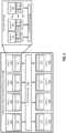
- Figure 2 illustrates hierarchical cache tags used to support die-level cache coherency in a multi-core, multi-thread processor.
- Figure 2 shows the organization of disclosed MCMT processing cores at the die level.
- hierarchical cache tags used to support die-level cache coherency.
- multi-core, multi-threaded (MCMT) processor die 200 includes eight cores, 204, 206, 208, 210, 212, 214, 216, and 218, which respectively include core shadow tags 205, 207, 209, 211, 213, 215, 217, and 219. All eight cores have a direct connection to a die shadow tag 220, which tracks the current state of (potentially) all cache lines in the eight cores at a per-core shadow tag granularity.
- Core 220 includes P pipelines, 222, 224, to 226, each of which is coupled to a data cache and data cache tags.
- Core 220 includes core shadow tag 211, which tracks (potentially) all of the cache lines in the data caches associated with the pipelines.
- Figure 3 illustrates cache coherency subdomains. Disclosed examples support and allow multiple (variably-sized) unique coherency domains within a single MCMT processor die, for example, as discussed below with respect to Figure 3 . Such coherency domains allow efficient coherency tracking and data sharing within small islands of a larger system.
- the full MCMT system may span multiple racks, where each rack consists of multiple nodes of 16-die sockets. Any address in the distributed global address system (DGAS) may be pulled into the coherent domain.
- DGAS distributed global address system
- the shadow tags provide a unit local to the caches that enables faster responses and promotes data sharing between caches within the core/die.
- disclosed examples useful for understanding the invention support a two level (local/global) coherency monitoring system with the core shadow tag and die shadow tag.
- the two-level arrangement allows for a reduction of long latency messages out to the die shadow tag when a shared cache line already exists at a core level.
- the disclosed multi-core, multi-system processor architecture supports the grouping of pipelines/cores into coherent sub-domains. These are configured via store operations to three machine-status registers (MSRs) that are visible in the MCMT processor address map.
- MSRs machine-status registers
- Table 1 lists the three MSRs, and their descriptions, width, and what level of the hierarchy they exist.
- Table 1 MSR Description Width (bits) Level CACHE_COHERENCY_EN This cache is participating in coherency.
- 1 Per-pipeline CORE_COHERENCY_EN This core shadow tag will send coherency messages to the die-shadow tag.
- 1 Per-core DOMAIN_ID If this cache is participating in coherency, this is the ID number of the sub-domain it is in. 5 Per-pipeline
- the size of the DOMAIN_ID MSR is determined by the maximum number of unique sub-domains that can be supported within the die.
- a single MCMT processor die has 48 individual caches (six caches per MCMT processing core, eight cores per die) and a sub-domain requires at least two caches to participate. Therefore, a single die may have up to 24 unique sub-domains.
- the MSRs are configured one time during program initialization. However, dynamic reconfiguration of the sub-domains is allowed. Whenever any modifications are made to the MSR values, the cache will switch into a flush state, where it will clear all of its contents (alerting the core shadow tag), writing back any lines in a dirty state.
- multi-core, multi-threaded (MCMT) processor core 300 includes six pipelines (or “pipes"), 304, 306, 308, 312, 314, and 316. All six pipes have a direct connection to a core shadow tag 320, which tracks the current state of (potentially) all cache lines in the six pipeline data caches, at a per-pipe shadow tag granularity. Of the six caches managed by core shadow tag 320, two, 304 and 312, are participating in sub-domain 1. Three pipes, 306, 314, and 316, are participating in sub-domain 2. A single cache, associated with pipe 308, has coherency disabled - making it private and meaning that it will send no requests to the core shadow tag.
- the core shadow tag has its internal arrays organized such that there is a 1:1 mapping to each cache in the core and these arrays are accessed based on the DOMAIN_ID MSR of that cache.
- the shadow tag will then only reference arrays that share the same ID. Accessing fewer than all of the arrays will lower read energy and total response time, assuming that the number of caches in that domain is less than the maximum. Additionally, requests coming to the shadow tag from caches in different sub-domains may be serviced in parallel.
- the single core shadow tag has the capability of serving as up to three unique sub-domain shadow tags (up to three tags correspond to the up to six pipes).
- the die shadow tag 220 will operate in the same way as the core shadow tags 320.
- the internal arrays also map at a 1:1 ratio to each cache in the die, meaning that they can be marked with the current DOMAIN_ID MSR value that was set for each cache. Requests received from core shadow tags 320 will come with the sub-domain ID, allowing the die shadow tag 220 to reduce energy consumption when possible.
- the die shadow tag 220 While the die shadow tag 220 has the maximum storage capability, it will only be used if every single cache in the die domain is holding its own unique line (i.e., no sharing). Otherwise, if a core has multiple caches sharing the line, it will occupy multiple core shadow tag entries 320 but only a single die shadow tag entry 220 (representing the entire core). This concept will be explained further below.
- MOESI-F cache coherency protocol which is further illustrated and described with respect to Figure 15 .
- the MOESI-F states are also defined below in Table 2.
- Table 2 State DESCRIPTION (M)odified Dirty cache line; Write-access; No other caches share.
- E xclusive Clean cache line; Read-only; No other caches share.
- S hared Clean cache line; Read-only; Other caches share.
- I nvalid Cache does not hold the line.
- F orward Clean cache line; Read-only; Other caches share; This cache forwards data.
- each RD or WR request would require a request sent to the core shadow tag and sub-sequentially to the die shadow tag so that the state change for that cache's line can be tracked in both units.
- the MCMT processor architecture implements local and global state tracking.
- the global state is that which is visible to the die shadow tag.
- the die shadow tag manages cache lines according to each MCMT processor core's global state and in full accordance with the previously described MOESI-F protocol.
- Each MCMT processor core (for a single domain ID) will have a single global state and cache-line tag entry in the die shadow tag, even if multiple caches within that core share the cache line.
- the core shadow tag will track both the global and local states for each cache's line in the shadow tag. Caches (within a core) that share a line may have different local states, but will always have the same global state. Table 3 shows the legal combinations of local and global states. Table 3 Global Local Notes M M/O/S Core is the only one with the dirty line (globally). Local O/S valid to share line within core. For cache to write, must be in global M and local M . O O/S Die shadow tag may request for local O cache to send data remote. E E/F/S Core is the only one with the clean line ( global ). Local F/S valid to share line within core. S S Can still share within core. Explained below. I I F F/S Die shadow tag may request for local F cache to send data remote.
- Local state may only be M if global state is M.
- MOESI-F coherency protocol dictates that only a single cache in the entire coherent domain may have write-ability. Allowing a local M without a global M would violate this requirement.
- Local state may only be E if global state is E.
- the protocol allows for a fast upgrade from E state to M state. This requires that only one E cache exists in the domain.
- MOESI-F MOESI-F protocol
- the protocol is designed such that a cache will always be in a designated forwarding state (F, O, E, or M). Allowing all local caches to be in S state creates a situation where no local cache is a designated forwarder. However, when a new local cache makes a request for the line, it is most optimal for performance to have a cache in the local MCMT processor core respond.
- the core shadow tag needs to determine: A) who will forward data to a new local cache asking for that cache line in "RD"; and B) who will assume F, O, M, or E state if the die shadow tag sends a "Float*" request and the core domain changes its global state to F/O/E/M. To determine this, the core shadow tag will select the S cache that is the lowest ordered pipeline in the core (i.e. pipeline 0, 1, 2...5).
- FIG. 4 is a flow diagram illustrating steps taken by a first pipeline of a multi-core, multi-thread (MCMT) processor to read a cache line.
- a flow of operations 400 is to be conducted by a first pipeline.
- the first pipeline is to initialize the system having R racks, each rack having N nodes, each node having D dies, each die having C cores and a die shadow tag array, each core having P pipelines and a core shadow tag array, each pipeline associated with a data cache and a data cache tag array, each data cache being either non-coherent or coherent, each coherent cache being associated with one of X coherency domains, and having cache lines with a modified, owned, exclusive, shared, invalid, or forward (MOESI-F) state
- MOESI-F modified, owned, exclusive, shared, invalid, or forward
- the first pipeline is to issue a request to read a cache line from its associated data cache.
- the first pipeline is to, if need be, issue a read request to its associated core-level cache.
- the first pipeline is to, if need be, issue a read request to its associated die.
- the first pipeline is to, if need be, issue a remote read request to a die mapped to the cache line.
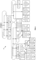
- FIG. 5 is a block flow diagram illustrating a coherence flow beginning with a read request to a data cache.
- flow 500 begins with a pipeline issuing a read (RD) request to a data cache at 502.
- the flow then transitions to one or more of operations 504, 506, 508, 510, 512, 514, 516, 518, and 520.
- Each of the transitions is controlled by the conditions listed on the arc showing the transition.
- the transition conditions sometimes include "L” or "G,” which as used herein refer to local or global state.
- flow 500 transitions from operation 502 to operation 504 if the cache state is any one of M, O, E, S, or F.
- a RD request to the data cache can be handled by only the core shadow tag.
- the only case where a message must be sent to the die shadow tag is when the global state is I. If this occurs, a RD request is sent to the die shadow tag, and the cache line is brought in locally as either global E or S.
- FIG. 6 is a block flow diagram illustrating a coherence flow beginning with a write (WR) request to a data cache.
- flow 600 begins with a pipeline issuing a WR request to a data cache at 602.
- the flow then transitions to one or more of operations 604, 606, 608, 610, 612, 614, 616, 618, 620, 622, 624, 626, 628, 630, 632, 634, 636, 638, and 640.
- Each of the transitions is controlled by the conditions listed on the arc showing the transition.
- the transition conditions sometimes include "L" or "G,” which as used herein refer to local or global state.
- flow 600 transitions from operation 602 to operation 604 if the cache state is any one of M, O, E, S, or F.
- FIG. 7 is a block flow diagram illustrating a coherency flow beginning with an evict request to a data cache.
- flow 700 begins with a pipeline issuing an EVICT request to a data cache at 702.
- the flow then transitions to one or more of operations 704, 706, 708, 710, 712, 714, 716, 718, 720, 721, 722, 724, 726, 727,728, 730, 731, 732, 734, 736, 737, 738, 740, 741, 742, 744, 745, 746, 747, 748, and 750.
- each of the transitions is controlled by the conditions listed on the arc showing the transition.
- the base organization of the disclosed multi-core, multi-threaded (MCMT) processing system hierarchy is structured as follows: six pipelines per MCMT core, eight MCMT cores per die, and 16 dies per socket. Each of these levels of the hierarchy also come with their own grouping of "local" on-die scratchpad (SP) and in-package memory (IPM). Each MCMT core has 2MB of scratchpad and a 2GB IPM channel, totaling 16MB-SP/16GB-IPM at the die level and 256MB-SP/256GB-IPM in a single socket. All memory is visible in the 64-bit MCMT processor address map and can be accessed from any pipeline in the DGAS system.
- SP on-die scratchpad
- IPM in-package memory
- the disclosed MCMT processor is designed as a system where selectively caching read-only (or private), heavily used data structures is the most optimal programming approach for solving cache-unfriendly graph applications. These workloads commonly consist of random, remote, small-granularity accesses and have little temporal or spatial locality.
- By setting bit-62 in the address a memory location will be brought into the pipeline's local data cache. If that bit is not set, the load or store request is sent directly to the memory location, which may be local (within the core or die) or remote (on a different die/socket/board/rack).
- the disclosed MCMT processor must still support legacy codes. This means that programming models that expect all accesses to be cached (and therefore coherent between processes) must still be supported with minimal modification.
- the invention described in this disclosure and implemented in the disclosed MCMT processor aims to address this goal.
- the highest boundary for cache coherency management in the MCMT system is at the die level.
- Each die has eight cores that have local coherency between their pipelines managed by a single core shadow tag unit.
- all eight MCMT processing cores may remain cache coherent through tracking at the die shadow tag unit.
- the architecture provides the programmer the ability to construct the organization of the coherent domain (or multiple coherent sub-domains) in a manner that most optimally supports their programming model.
- the high-level process will take the following steps.
- the requesting cache will be referred to as cache-1.
- the remote cache who owns the data in their coherent domain will be referred to as cache-2.
- the disclosed multi-core, multi-threaded (MCMT) system provides a no-cache remote policy for inter-die memory accesses.
- the data cache will check for the memory address locality (i.e., is address in its die) before determining if the data will be brought into its coherent domain or accessed with a no-cache remote request.
- the data that is read from or written to will be the most recent copy of coherent data within that die. This is done through the combined use of a no-cache remote engine and the disclosed MCMT die-level shadow tag, which manages die cache coherency traffic.
- the data will not be stored in the requesting cache, to ensure that it will always see the most recent coherent copy for each no-cache remote access.
- the disclosed MCMT system's no-cache remote implementation provides a bridge between the two methods by giving the most recent coherent data on an inter-die memory access and ensuring memory correctness on writes.
- the policy has minimal area overheads and limits long-latency die-to-die messages to manage performance overheads.
- the disclosed multi-core, multi-threaded (MCMT) processing system implements a no-cache remote memory policy.
- MCMT multi-core, multi-threaded
- the data cache receives a request to a scratchpad or IPM address that is located within its die, it will be brought in to the cache and managed by the MCMT core hardware cache coherency protocol. But, if the address is not local to the data cache's die, the data cache will send the load or store as a "no-cache remote" request to the remote die's die-level shadow tag.
- the shadow tag is then responsible for facilitating the return of the most recent (coherent) copy of data for a load, or correctly writing the data to memory (ensuring correctness) for a store request.
- This protocol accomplishes two main goals:
- Activating the no-cache remote policy is done through setting an enable machine-status register (MSR) bit that is accessible through the address map. If the enable bit is not set, the data cache will service all cache requests as regular cache-able addresses that are brought into the coherency domain. This will require software memory management for remote-die requests which may cross coherent domains.
- MSR machine-status register
- the data cache When executing the no-cache remote policy, the data cache will check for address locality by comparing the requested memory address with its DIE_LOCATION address MSR.
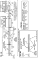
- This MSR is configured at system boot, unique to each of the disclosed MCMT processor die, and shared by all multi-threaded cores within a MCMT processor die. The comparison is performed based on the organization of the disclosed MCMT processor address map. A section of this address map is shown in Figure 8A . The organization dictates that the observed location of the die ID changes depending on if the targeted memory is IPM or scratchpad according to the following two cases:
- bits [44:42] are supported. They stand as holes in the address map but are reserved for additional memory that may be added to the system.
- Figure 8A is a portion of an address map targeting a specific die's IPM or scratchpad.
- No-Cache Remote (NCR) Engine is located in the address map in Core 0 of each die. The full address needed to target this location is shown in Figure 8B .
- Figure 8B is an address targeting a no-cache remote engine.
- the request information included in the no-cache remote packet is shown in Table 4. This information is sent to the NCR engine and is necessary to fully execute the request and return the proper response.
- the total size of the request packet is 193 bits.
- Table 4 Field DESCRIPTION Destination Address Address of memory location that cache wants to read from/write to. Source Address Address of data cache making request.
- Request Type Either no-cache remote load or store request. Data If is it a store request, 8-Byte data element to store.
- the NCR engine serves as the management unit for accessing the die shadow tag unit and executing the request. It has the following responsibilities:
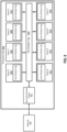
- FIG. 9 is a block diagram illustrating inclusion of a no-cache remote engine interface.
- multi-core, multi-threaded (MCMT) processor die 900 includes 8 cores, 904, 906, 908, 910, 912, 914, 916, and 918. Each of the cores has a core shadow tag.
- MCMT processor die 900 further includes a die shadow tag 920 and a no-cache remote (NCR) engine 902, which is capable of sending requests over network 903.
- NCR no-cache remote
- the logical connection of the no-cache remote engine to the die shadow tag and its port out to the MCMT network It is through this port that it will receive requests from remote dies, as well as issue load and store requests to memory - the usage of these requests is further described below.
- Non-conflicting requests are serviced from all ports in parallel, if requests from different ports have an address conflict, they are serialized based on core order (i.e. core 0, 1, 2, etc.). The no-cache remote engine will have lowest priority in these cases.
- the NCR engine requires two new request types to be supported by the die shadow tag: Remote RD and Remote WR. These instructions will initiate functionality within the die shadow tag that varies only slightly from the currently supported flows. The functionality dictates that the die shadow tag will perform an address match of the contents of the domains it is managing. It is possible that multiple die sub-domains will hold the same cache line. If this is the case, the die shadow tag will have the lowest ordered sub-domain (domain ID 0,1,2, etc.) respond to the request. To avoid this scenario, software will be expected to properly manage memory that crosses within-die coherent sub-domain boundaries.
- Figure 10 is a block flow diagram illustrating a die shadow tag decision flow when responding to a remote read request received from an NCR engine.
- flow 1000 begins at 1002, when the die shadow tag receives a remote RD request from the NCR engine, the NCR engine having received the remote RD request over a network from a remote data cache pipeline of a remote die.
- NCR engine 902 uses its dedicated port into die shadow tag 920 to forward the remote RD request, along with an identifier of the source of the request.
- die shadow tag 920 has nine ports, allowing the eight cores and the NCR engine to access the die shadow tags in parallel.
- the die shadow tag state of the requested address is checked.
- the die shadow tag at 1006 returns a "no-sharers exist" response to the NCR engine.
- the MOESI-F protocol dictates that it will be in one of M, O, F, or E states. If the requested address is valid, the die shadow tag at 1008 returns a "sharers do exist" response to the NCR engine.
- the die shadow tag at 1010 will tell that owning cache to forward the cache line to the remote die's cache that made the no-cache remote RD request (the die shadow tag knows and tells the owning cache where to forward the data because the NCR engine receives a source address with the no-cache remote RD request, and forwards that source address to the die shadow tag along with the request). In that case, the die shadow tag will also inform the NCR engine that "sharers exist.” Note, it is not possible for only S state core shadow tags to exist (i.e., a designated responder must exist).
- the no-cache remote (NCR) engine Upon receiving a response from the die shadow tag, the no-cache remote (NCR) engine will proceed in one of two ways. If a "no-sharers" response is received, this indicates that the data must be fetched from memory. The NCR engine will send a load request to that memory location (on the same die), indicating that the return address will be the original remote data cache that made the request. The loaded data returning to that data cache will indicate the end of the operation. If a "sharers-exist" response is returned from the die shadow tag, the NCR engine is no longer needed, and will clear its slot. Here, the owning cache (M/O/E or F state) sends the data directly back to the remote requesting cache, the data arriving at that cache indicates the end of the operation.
- M/O/E or F state sends the data directly back to the remote requesting cache, the data arriving at that cache indicates the end of the operation.
- FIG 11 is a block flow diagram illustrating a die shadow tag decision flow when responding to a remote write request received from an NCR engine.
- flow 1100 begins at 1102, when the NCR engine forwards a remote WR request to the die shadow tag, the NCR engine having received the remote WR request over a network from a remote data cache pipeline of a remote die.
- the die shadow tag at 1104 checks the die shadow tag state. If the cache line is invalid in the die's coherent domain, the die shadow tag at 1106 notifies the NCR engine (i.e., "no-sharers") and the store request is sent from the NCR engine to memory.
- the die shadow tag, in the interest of data correctness, at 1108 waits for an ACK (Acknowledgment) from the NCR engine indicating that the store was completed.
- ACK Acknowledgment
- the cache line is in the coherent domain in a clean state (F or E)
- all shared cache lines are invalidated at 1110, and at 1112 a "no sharers" response is sent to the NCR engine, causing the NCR engine to send the store to memory.
- the die shadow tag at 1114 waits for an ACK from the NCR engine that the store was completed.
- the M/O cache is directed at 1116 to write back the dirty line (invalidating the line in the cache), and all caches with the line (in S state) are invalidated.
- the die shadow tag informs the NCR engine, who sends the store to the memory. The die shadow tag at 1122 then waits for an ACK from the NCR engine that the store was completed.
- Figure 12 illustrates a state flow diagram for the MOESI-F ( M odified O wned E xclusive S hared I nvalid F orward) cache coherency protocol.
- the states included are M (Modified) 1202, O (Owned) 1204, F (Forward) 1206, E (Exclusive) 1208, S (Shared) 1210, and I (Invalid) 1212.
- cache line data responses to read (“GetS”) or write (“GetM”) requests can come from caches in the E, F, O, or M states, via routes 1270, 1274, and 1288 from the E state, route 1290 from the F state, routes 1282 and 1292 from the O state, and route 1278 from the M state. In these states for each line, it is ensured that there is always a single responder for either type of request.
- An eviction of a line in O follows the same concept.
- the cache in O is evicted, for example at 1292, one of the caches in S will transition to O, such as at 1262. If only one S cache exists, that cache will instead transition to M, such as at 1266, maintaining within the protocol that only a cache in M will write-back to memory if it is evicted, such as at 1278.
- the O state serves as the F state for dirty data. All responses to read requests for shared data (GetS), will be handled by the O state (dirty) or the F state (clean). Since two sharing lines cannot exist in O and F together, if a cache in one of these states receives a GetS, it will instantly respond with the data. Additionally, transitions away from the O and F state are identical, as can be seen in Figure 12 . Because of this, and the identical process of passing the state to an S cache on an eviction, the complexity and implementation overhead of having both the F and O states is very small.
- An instruction set may include one or more instruction formats.
- a given instruction format may define various fields (e.g., number of bits, location of bits) to specify, among other things, the operation to be performed (e.g., opcode) and the operand(s) on which that operation is to be performed and/or other data field(s) (e.g., mask).
- Some instruction formats are further broken down though the definition of instruction templates (or subformats).
- the instruction templates of a given instruction format may be defined to have different subsets of the instruction format's fields (the included fields are typically in the same order, but at least some have different bit positions because there are less fields included) and/or defined to have a given field interpreted differently.
- each instruction of an ISA is expressed using a given instruction format (and, if defined, in a given one of the instruction templates of that instruction format) and includes fields for specifying the operation and the operands.
- an exemplary ADD instruction has a specific opcode and an instruction format that includes an opcode field to specify that opcode and operand fields to select operands (source1/destination and source2); and an occurrence of this ADD instruction in an instruction stream will have specific contents in the operand fields that select specific operands.
- a set of SIMD extensions referred to as the Advanced Vector Extensions (AVX) (AVX1 and AVX2) and using the Vector Extensions (VEX) coding scheme has been released and/or published (e.g., see Intel ® 64 and IA-32 Architectures Software Developer's Manual, September 2014 ; and see Intel® Advanced Vector Extensions Programming Reference, October 2014 ).
- instruction(s) described herein may be embodied in different formats.
- exemplary systems, architectures, and pipelines are detailed below. Examples useful for understanding the invention of the instruction(s) may be executed on such systems, architectures, and pipelines, but are not limited to those detailed.
- a vector friendly instruction format is an instruction format that is suited for vector instructions (e.g., there are certain fields specific to vector operations). While examples useful for understanding the invention are described in which both vector and scalar operations are supported through the vector friendly instruction format, alternative examples useful for understanding the invention use only vector operations the vector friendly instruction format.
- Figures 13A-13B are block diagrams illustrating a generic vector friendly instruction format and instruction templates thereof.
- Figure 13A is a block diagram illustrating a generic vector friendly instruction format and class A instruction templates thereof; while Figure 13B is a block diagram illustrating the generic vector friendly instruction format and class B instruction templates thereof.
- the term generic in the context of the vector friendly instruction format refers to the instruction format not being tied to any specific instruction set.
- a 64 byte vector operand length (or size) with 32 bit (4 byte) or 64 bit (8 byte) data element widths (or sizes) (and thus, a 64 byte vector consists of either 16 doubleword-size elements or alternatively, 8 quadword-size elements); a 64 byte vector operand length (or size) with 16 bit (2 byte) or 8 bit (1 byte) data element widths (or sizes); a 32 byte vector operand length (or size) with 32 bit (4 byte), 64 bit (8 byte), 16 bit (2 byte), or 8 bit (1 byte) data element widths (or sizes); and a 16 byte vector operand length (or size) with 32 bit (4 byte), 64 bit (8 byte), 16 bit (2 byte), or 8 bit (1 byte) data element widths (or sizes); and a 16 byte vector operand length (or size) with 32 bit (4 byte), 64 bit (8 byte), 16 bit (2 byte), or 8 bit (1 byte) data element widths (or sizes); alternative examples useful for understanding the invention may support more
- the class A instruction templates in Figure 13A include: 1) within the no memory access 1305 instruction templates there is shown a no memory access, full round control type operation 1310 instruction template and a no memory access, data transform type operation 1315 instruction template; and 2) within the memory access 1320 instruction templates there is shown a memory access, temporal 1325 instruction template and a memory access, non-temporal 1330 instruction template.
- the class B instruction templates in Figure 13B include: 1) within the no memory access 1305 instruction templates there is shown a no memory access, write mask control, partial round control type operation 1312 instruction template and a no memory access, write mask control, vsize type operation 1317 instruction template; and 2) within the memory access 1320 instruction templates there is shown a memory access, write mask control 1327 instruction template.
- the generic vector friendly instruction format 1300 includes the following fields listed below in the order illustrated in Figures 13A-13B .
- Format field 1340 - a specific value (an instruction format identifier value) in this field uniquely identifies the vector friendly instruction format, and thus occurrences of instructions in the vector friendly instruction format in instruction streams. As such, this field is optional in the sense that it is not needed for an instruction set that has only the generic vector friendly instruction format.
- Base operation field 1342 its content distinguishes different base operations.
- Register index field 1344 its content, directly or through address generation, specifies the locations of the source and destination operands, be they in registers or in memory. These include a sufficient number of bits to select N registers from a PxQ (e.g. 32x512, 16x128, 32x1024, 64x1024) register file. While in one example useful for understanding the invention N may be up to three sources and one destination register, alternative examples useful for understanding the invention may support more or less sources and destination registers (e.g., may support up to two sources where one of these sources also acts as the destination, may support up to three sources where one of these sources also acts as the destination, may support up to two sources and one destination).
- PxQ e.g. 32x512, 16x128, 32x1024, 64x1024
- Modifier field 1346 its content distinguishes occurrences of instructions in the generic vector instruction format that specify memory access from those that do not; that is, between no memory access 1305 instruction templates and memory access 1320 instruction templates.
- Memory access operations read and/or write to the memory hierarchy (in some cases specifying the source and/or destination addresses using values in registers), while non-memory access operations do not (e.g., the source and destinations are registers). While in one example useful for understanding the invention this field also selects between three different ways to perform memory address calculations, alternative examples useful for understanding the invention may support more, less, or different ways to perform memory address calculations.
- Augmentation operation field 1350 its content distinguishes which one of a variety of different operations to be performed in addition to the base operation. This field is context specific. For example, this field is divided into a class field 1368, an alpha field 1352, and a beta field 1354.
- the augmentation operation field 1350 allows common groups of operations to be performed in a single instruction rather than 2, 3, or 4 instructions.
- Scale field 1360 - its content allows for the scaling of the index field's content for memory address generation (e.g., for address generation that uses 2 scale ⁇ index + base).
- Displacement Field 1362A- its content is used as part of memory address generation (e.g., for address generation that uses 2 scale ⁇ index + base + displacement).
- Displacement Factor Field 1362B (note that the juxtaposition of displacement field 1362A directly over displacement factor field 1362B indicates one or the other is used) - its content is used as part of address generation; it specifies a displacement factor that is to be scaled by the size of a memory access (N) - where N is the number of bytes in the memory access (e.g., for address generation that uses 2 scale ⁇ index + base + scaled displacement). Redundant low-order bits are ignored and hence, the displacement factor field's content is multiplied by the memory operands total size (N) in order to generate the final displacement to be used in calculating an effective address.
- N is determined by the processor hardware at runtime based on the full opcode field 1374 (described later herein) and the data manipulation field 1354C.
- the displacement field 1362A and the displacement factor field 1362B are optional in the sense that they are not used for the no memory access 1305 instruction templates and/or different examples useful for understanding the invention may implement only one or none of the two.
- Data element width field 1364 its content distinguishes which one of a number of data element widths is to be used (in some examples useful for understanding the invention for all instructions; in other examples useful for understanding the invention for only some of the instructions). This field is optional in the sense that it is not needed if only one data element width is supported and/or data element widths are supported using some aspect of the opcodes.
- Write mask field 1370 its content controls, on a per data element position basis, whether that data element position in the destination vector operand reflects the result of the base operation and augmentation operation.
- Class A instruction templates support merging-writemasking
- class B instruction templates support both merging- and zeroing-writemasking.
- any set of elements in the destination when zeroing vector masks allow any set of elements in the destination to be zeroed during the execution of any operation (specified by the base operation and the augmentation operation); in one example useful for understanding the invention, an element of the destination is set to 0 when the corresponding mask bit has a 0 value.
- a subset of this functionality is the ability to control the vector length of the operation being performed (that is, the span of elements being modified, from the first to the last one); however, it is not necessary that the elements that are modified be consecutive.
- the write mask field 1370 allows for partial vector operations, including loads, stores, arithmetic, logical, etc.
- Immediate field 1372 its content allows for the specification of an immediate. This field is optional in the sense that is it not present in an implementation of the generic vector friendly format that does not support immediate and it is not present in instructions that do not use an immediate.
- Class field 1368 its content distinguishes between different classes of instructions. With reference to Figures 13A-B, the contents of this field select between class A and class B instructions. In Figures 13A-B , rounded corner squares are used to indicate a specific value is present in a field (e.g., class A 1368A and class B 1368B for the class field 1368 respectively in Figures 13A-B ).
- the alpha field 1352 is interpreted as an RS field 1352A, whose content distinguishes which one of the different augmentation operation types are to be performed (e.g., round 1352A.1 and data transform 1352A.2 are respectively specified for the no memory access, round type operation 1310 and the no memory access, data transform type operation 1315 instruction templates), while the beta field 1354 distinguishes which of the operations of the specified type is to be performed.
- the scale field 1360, the displacement field 1362A, and the displacement factor field 1362B are not present.
- the beta field 1354 is interpreted as a round control field 1354A, whose content(s) provide static rounding. While in the described examples useful for understanding the invention the round control field 1354A includes a suppress all floating-point exceptions (SAE) field 1356 and a round operation control field 1358, alternative examples useful for understanding the invention may support may encode both these concepts into the same field or only have one or the other of these concepts/fields (e.g., may have only the round operation control field 1358).
- SAE suppress all floating-point exceptions
- SAE field 1356 its content distinguishes whether or not to disable the exception event reporting; when the SAE field's 1356 content indicates suppression is enabled, a given instruction does not report any kind of floating-point exception flag and does not raise any floating-point exception handler.
- Round operation control field 1358 its content distinguishes which one of a group of rounding operations to perform (e.g., Round-up, Round-down, Round-towards-zero and Round-to-nearest).
- the round operation control field 1358 allows for the changing of the rounding mode on a per instruction basis.
- the round operation control field's 1350 content overrides that register value.
- the beta field 1354 is interpreted as a data transform field 1354B, whose content distinguishes which one of a number of data transforms is to be performed (e.g., no data transform, swizzle, broadcast).
- the alpha field 1352 is interpreted as an eviction hint field 1352B, whose content distinguishes which one of the eviction hints is to be used (in Figure 13A , temporal 1352B.1 and non-temporal 1352B.2 are respectively specified for the memory access, temporal 1325 instruction template and the memory access, non-temporal 1330 instruction template), while the beta field 1354 is interpreted as a data manipulation field 1354C, whose content distinguishes which one of a number of data manipulation operations (also known as primitives) is to be performed (e.g., no manipulation; broadcast; up conversion of a source; and down conversion of a destination).
- the memory access 1320 instruction templates include the scale field 1360, and optionally the displacement field 1362A or the displacement factor field 1362B.
- Vector memory instructions perform vector loads from and vector stores to memory, with conversion support. As with regular vector instructions, vector memory instructions transfer data from/to memory in a data element-wise fashion, with the elements that are actually transferred is dictated by the contents of the vector mask that is selected as the write mask.
- Temporal data is data likely to be reused soon enough to benefit from caching. This is, however, a hint, and different processors may implement it in different ways, including ignoring the hint entirely.
- Non-temporal data is data unlikely to be reused soon enough to benefit from caching in the 1st-level cache and should be given priority for eviction. This is, however, a hint, and different processors may implement it in different ways, including ignoring the hint entirely.
- the alpha field 1352 is interpreted as a write mask control (Z) field 1352C, whose content distinguishes whether the write masking controlled by the write mask field 1370 should be a merging or a zeroing.
- part of the beta field 1354 is interpreted as an RL field 1357A, whose content distinguishes which one of the different augmentation operation types are to be performed (e.g., round 1357A.1 and vector length (VSIZE) 1357A.2 are respectively specified for the no memory access, write mask control, partial round control type operation 1312 instruction template and the no memory access, write mask control, VSIZE type operation 1317 instruction template), while the rest of the beta field 1354 distinguishes which of the operations of the specified type is to be performed.
- the scale field 1360, the displacement field 1362A, and the displacement factor field 1362B are not present.
- Round operation control field 1359A just as round operation control field 1358, its content distinguishes which one of a group of rounding operations to perform (e.g., Round-up, Round-down, Round-towards-zero and Round-to-nearest).
- the round operation control field 1359A allows for the changing of the rounding mode on a per instruction basis.
- the round operation control field's 1350 content overrides that register value.
- the rest of the beta field 1354 is interpreted as a vector length field 1359B, whose content distinguishes which one of a number of data vector lengths is to be performed on (e.g., 128, 256, or 512 byte).
- a memory access 1320 instruction template of class B part of the beta field 1354 is interpreted as a broadcast field 1357B, whose content distinguishes whether or not the broadcast type data manipulation operation is to be performed, while the rest of the beta field 1354 is interpreted the vector length field 1359B.
- the memory access 1320 instruction templates include the scale field 1360, and optionally the displacement field 1362A or the displacement factor field 1362B.
- a full opcode field 1374 is shown including the format field 1340, the base operation field 1342, and the data element width field 1364. While one example useful for understanding the invention is shown where the full opcode field 1374 includes all of these fields, the full opcode field 1374 includes less than all of these fields in examples useful for understanding the invention that do not support all of them.
- the full opcode field 1374 provides the operation code (opcode).
- the augmentation operation field 1350, the data element width field 1364, and the write mask field 1370 allow these features to be specified on a per instruction basis in the generic vector friendly instruction format.
- write mask field and data element width field create typed instructions in that they allow the mask to be applied based on different data element widths.
- processors or different cores within a processor may support only class A, only class B, or both classes.
- a high performance general purpose out-of-order core intended for general-purpose computing may support only class B
- a core intended primarily for graphics and/or scientific (throughput) computing may support only class A
- a core intended for both may support both (of course, a core that has some mix of templates and instructions from both classes but not all templates and instructions from both classes is within the purview of the invention).
- a single processor may include multiple cores, all of which support the same class or in which different cores support different class.
- one of the graphics cores intended primarily for graphics and/or scientific computing may support only class A, while one or more of the general purpose cores may be high performance general purpose cores with out of order execution and register renaming intended for general-purpose computing that support only class B.
- Another processor that does not have a separate graphics core may include one more general purpose in-order or out-of-order cores that support both class A and class B.
- features from one class may also be implement in the other class in different examples useful for understanding the invention.
- Programs written in a high level language would be put (e.g., just in time compiled or statically compiled) into an variety of different executable forms, including: 1) a form having only instructions of the class(es) supported by the target processor for execution; or 2) a form having alternative routines written using different combinations of the instructions of all classes and having control flow code that selects the routines to execute based on the instructions supported by the processor which is currently executing the code.
- Figure 14A is a block diagram illustrating an exemplary specific vector friendly instruction format.
- Figure 14A shows a specific vector friendly instruction format 1400 that is specific in the sense that it specifies the location, size, interpretation, and order of the fields, as well as values for some of those fields.
- the specific vector friendly instruction format 1400 may be used to extend the x86 instruction set, and thus some of the fields are similar or the same as those used in the existing x86 instruction set and extension thereof (e.g., AVX). This format remains consistent with the prefix encoding field, real opcode byte field, MOD R/M field, SIB field, displacement field, and immediate fields of the existing x86 instruction set with extensions.
- the fields from Figure 13 into which the fields from Figure 14A map are illustrated.
- the invention is not limited to the specific vector friendly instruction format 1400 except where claimed.
- the generic vector friendly instruction format 1300 contemplates a variety of possible sizes for the various fields, while the specific vector friendly instruction format 1400 is shown as having fields of specific sizes.
- the data element width field 1364 is illustrated as a one bit field in the specific vector friendly instruction format 1400, the invention is not so limited (that is, the generic vector friendly instruction format 1300 contemplates other sizes of the data element width field 1364).
- the generic vector friendly instruction format 1300 includes the following fields listed below in the order illustrated in Figure 14A .
- EVEX Prefix (Bytes 0-3) 1402 is encoded in a four-byte form.
- EVEX Byte 0 bits [7:0]
- EVEX Byte 0 the first byte
- 0x62 the unique value used for distinguishing the vector friendly instruction format in some examples useful for understanding the invention
- the second-fourth bytes include a number of bit fields providing specific capability.
- REX field 1405 (EVEX Byte 1, bits [7-5]) - consists of an EVEX.R bit field (EVEX Byte 1, bit [7] - R), EVEX.X bit field (EVEX byte 1, bit [6] - X), and EVEX.B bit field (EVEX byte 1, bit [5] - B).
- the EVEX.R, EVEX.X, and EVEX.B bit fields provide the same functionality as the corresponding VEX bit fields, and are encoded using 1s complement form, i.e. ZMM0 is encoded as 1111B, ZMM15 is encoded as 0000B.
- Rrrr, xxx, and bbb may be formed by adding EVEX.R, EVEX.X, and EVEX.B.
- REX' 1410A - this is the first part of the REX' field 1410 and is the EVEX.R' bit field (EVEX Byte 1, bit [4] - R') that is used to encode either the upper 16 or lower 16 of the extended 32 register set.
- EVEX Byte 1, bit [4] - R' EVEX Byte 1, bit [4] - R'
- this bit along with others as indicated below, is stored in bit inverted format to distinguish (in the well-known x86 32-bit mode) from the BOUND instruction, whose real opcode byte is 62, but does not accept in the MOD R/M field (described below) the value of 11 in the MOD field; alternative examples useful for understanding the invention do not store this and the other indicated bits below in the inverted format.
- a value of 1 is used to encode the lower 16 registers.
- R'Rrrr is formed by combining EVEX.R', EVEX.R, and the other RRR from other fields.
- Opcode map field 1415 (EVEX byte 1, bits [3:0] - 10m) - its content encodes an implied leading opcode byte (0F, 0F 38, or 0F 3).
- Data element width field 1364 (EVEX byte 2, bit [7] - W) - is represented by the notation EVEX.W.
- EVEX.W is used to define the granularity (size) of the datatype (either 32-bit data elements or 64-bit data elements).
- EVEX.vvvv 1420 (EVEX Byte 2, bits [6:3]-vvvv)- the role of EVEX.vvvv may include the following: 1) EVEX.vvvv encodes the first source register operand, specified in inverted (1s complement) form and is valid for instructions with 2 or more source operands; 2) EVEX.vvvv encodes the destination register operand, specified in 1s complement form for certain vector shifts; or 3) EVEX.vvvv does not encode any operand, the field is reserved and should contain 1111b.
- EVEX.vvvv field 1420 encodes the 4 low-order bits of the first source register specifier stored in inverted (1s complement) form. Depending on the instruction, an extra different EVEX bit field is used to extend the specifier size to 32 registers.
- Prefix encoding field 1425 (EVEX byte 2, bits [1:0]-pp) - provides additional bits for the base operation field. In addition to providing support for the legacy SSE instructions in the EVEX prefix format, this also has the benefit of compacting the SIMD prefix (rather than requiring a byte to express the SIMD prefix, the EVEX prefix requires only 2 bits).
- legacy SIMD prefixes are encoded into the SIMD prefix encoding field; and at runtime are expanded into the legacy SIMD prefix prior to being provided to the decoder's PLA (so the PLA can execute both the legacy and EVEX format of these legacy instructions without modification).
- newer instructions could use the EVEX prefix encoding field's content directly as an opcode extension, certain examples useful for understanding the invention expand in a similar fashion for consistency but allow for different meanings to be specified by these legacy SIMD prefixes.
- An alternative example useful for understanding the invention may redesign the PLA to support the 2 bit SIMD prefix encodings, and thus not require the expansion.
- Alpha field 1352 (EVEX byte 3, bit [7] - EH; also known as EVEX.EH, EVEX.rs, EVEX.RL, EVEX.write mask control, and EVEX.N; also illustrated with ⁇ ) - as previously described, this field is context specific.
- Beta field 1354 (EVEX byte 3, bits [6:4]-SSS, also known as EVEX.s 2-0 , EVEX.r 2-0 , EVEX.rr1, EVEX.LL0, EVEX.LLB; also illustrated with ⁇ ) - as previously described, this field is context specific.
- REX' 1410B - this is the remainder of the REX' field 1410 and is the EVEX.V' bit field (EVEX Byte 3, bit [3] - V') that may be used to encode either the upper 16 or lower 16 of the extended 32 register set. This bit is stored in bit inverted format. A value of 1 is used to encode the lower 16 registers.
- V'VVVV is formed by combining EVEX.V', EVEX.vvvv.
- Write mask field 1370 (EVEX byte 3, bits [2:0]-kkk) - its content specifies the index of a register in the write mask registers as previously described.
- Real Opcode Field 1430 (Byte 4) is also known as the opcode byte. Part of the opcode is specified in this field.
- MOD R/M Field 1440 (Byte 5) includes MOD field 1442, Reg field 1444, and R/M field 1446. As previously described, the MOD field's 1442 content distinguishes between memory access and non-memory access operations.
- the role of Reg field 1444 can be summarized to two situations: encoding either the destination register operand or a source register operand or be treated as an opcode extension and not used to encode any instruction operand.
- the role of R/M field 1446 may include the following: encoding the instruction operand that references a memory address or encoding either the destination register operand or a source register operand.
- Scale, Index, Base (SIB) Byte (Byte 6) As previously described, the scale field's 1350 content is used for memory address generation. SIB.xxx 1454 and SIB.bbb 1456 - the contents of these fields have been previously referred to with regard to the register indexes Xxxx and Bbbb.
- Displacement field 1362A (Bytes 7-10) - when MOD field 1442 contains 10, bytes 7-10 are the displacement field 1362A, and it works the same as the legacy 32-bit displacement (disp32) and works at byte granularity.
- Displacement factor field 1362B (Byte 7) - when MOD field 1442 contains 01, byte 7 is the displacement factor field 1362B.
- the location of this field is that same as that of the legacy x86 instruction set 8-bit displacement (disp8), which works at byte granularity. Since disp8 is sign extended, it can only address between -128 and 127 bytes offsets; in terms of 64 byte cache lines, disp8 uses 8 bits that can be set to only four really useful values -128, -64, 0, and 64; since a greater range is often needed, disp32 is used; however, disp32 requires 4 bytes.
- the displacement factor field 1362B is a reinterpretation of disp8; when using displacement factor field 1362B, the actual displacement is determined by the content of the displacement factor field multiplied by the size of the memory operand access (N). This type of displacement is referred to as disp8*N. This reduces the average instruction length (a single byte of used for the displacement but with a much greater range). Such compressed displacement is based on the assumption that the effective displacement is multiple of the granularity of the memory access, and hence, the redundant low-order bits of the address offset do not need to be encoded. In other words, the displacement factor field 1362B substitutes the legacy x86 instruction set 8-bit displacement.
- the displacement factor field 1362B is encoded the same way as an x86 instruction set 8-bit displacement (so no changes in the ModRM/SIB encoding rules) with the only exception that disp8 is overloaded to disp8*N. In other words, there are no changes in the encoding rules or encoding lengths but only in the interpretation of the displacement value by hardware (which needs to scale the displacement by the size of the memory operand to obtain a byte-wise address offset).
- Immediate field 1372 operates as previously described.
- Figure 14B is a block diagram illustrating the fields of the specific vector friendly instruction format 1400 that make up the full opcode field 1374.
- the full opcode field 1374 includes the format field 1340, the base operation field 1342, and the data element width (W) field 1364.
- the base operation field 1342 includes the prefix encoding field 1425, the opcode map field 1415, and the real opcode field 1430.
- Figure 14C is a block diagram illustrating the fields of the specific vector friendly instruction format 1400 that make up the register index field 1344.
- the register index field 1344 includes the REX field 1405, the REX' field 1410, the MODR/M.reg field 1444, the MODR/M.r/m field 1446, the VVVV field 1420, xxx field 1454, and the bbb field 1456.
- Figure 14D is a block diagram illustrating the fields of the specific vector friendly instruction format 1400 that make up the augmentation operation field 1350.
- class (U) field 1368 contains 0, it signifies EVEX.U0 (class A 1368A); when it contains 1, it signifies EVEX.U1 (class B 1368B).
- the alpha field 1352 (EVEX byte 3, bit [7] - EH) is interpreted as the rs field 1352A.
- the beta field 1354 EVEX byte 3, bits [6:4]- SSS
- the round control field 1354A is interpreted as the round control field 1354A.
- the round control field 1354A includes a one bit SAE field 1356 and a two bit round operation field 1358.
- the beta field 1354 (EVEX byte 3, bits [6:4]-SSS) is interpreted as a three bit data transform field 1354B.
- the alpha field 1352 (EVEX byte 3, bit [7] - EH) is interpreted as the eviction hint (EH) field 1352B and the beta field 1354 (EVEX byte 3, bits [6:4]- SSS) is interpreted as a three bit data manipulation field 1354C.
- the alpha field 1352 (EVEX byte 3, bit [7] - EH) is interpreted as the write mask control (Z) field 1352C.
- the MOD field 1442 contains 11 (signifying a no memory access operation)
- part of the beta field 1354 (EVEX byte 3, bit [4]- S 0 ) is interpreted as the RL field 1357A; when it contains a 1 (round 1357A.1) the rest of the beta field 1354 (EVEX byte 3, bit [6-5]- S 2-1 ) is interpreted as the round operation field 1359A, while when the RL field 1357A contains a 0 (VSIZE 1357.A2) the rest of the beta field 1354 (EVEX byte 3, bit [6-5]- S 2-1 ) is interpreted as the vector length field 1359B (EVEX byte 3, bit [6-5]- L 1-0 ).
- the beta field 1354 (EVEX byte 3, bits [6:4]- SSS) is interpreted as the vector length field 1359B (EVEX byte 3, bit [6-5]- L 1-0 ) and the broadcast field 1357B (EVEX byte 3, bit [4]- B).
- Figure 15 is a block diagram of a register architecture 1500.
- the lower order 256 bits of the lower 16 zmm registers are overlaid on registers ymm0-16.
- the lower order 128 bits of the lower 16 zmm registers (the lower order 128 bits of the ymm registers) are overlaid on registers xmm0-15.
- the specific vector friendly instruction format 1400 operates on these overlaid register file as illustrated in the below tables.
- the vector length field 1359B selects between a maximum length and one or more other shorter lengths, where each such shorter length is half the length of the preceding length; and instructions templates without the vector length field 1359B operate on the maximum vector length.
- the class B instruction templates of the specific vector friendly instruction format 1400 operate on packed or scalar single/double-precision floating-point data and packed or scalar integer data. Scalar operations are operations performed on the lowest order data element position in an zmm/ymm/xmm register; the higher order data element positions are either left the same as they were prior to the instruction or zeroed depending on the example useful for understanding the invention.
- Scalar floating-point stack register file (x87 stack) 1545 on which is aliased the MMX packed integer flat register file 1550 - in the example useful for understanding the invention illustrated, the x87 stack is an eight-element stack used to perform scalar floating-point operations on 32/64/80-bit floating-point data using the x87 instruction set extension; while the MMX registers are used to perform operations on 64-bit packed integer data, as well as to hold operands for some operations performed between the MMX and XMM registers.
- Alternative examples useful for understanding the invention may use wider or narrower registers. Additionally, alternative examples useful for understanding the invention may use more, less, or different register files and registers.
- Processor cores may be implemented in different ways, for different purposes, and in different processors.
- implementations of such cores may include: 1) a general purpose in-order core intended for general-purpose computing; 2) a high performance general purpose out-of-order core intended for general-purpose computing; 3) a special purpose core intended primarily for graphics and/or scientific (throughput) computing.
- Implementations of different processors may include: 1) a CPU including one or more general purpose in-order cores intended for general-purpose computing and/or one or more general purpose out-of-order cores intended for general-purpose computing; and 2) a coprocessor including one or more special purpose cores intended primarily for graphics and/or scientific (throughput).
- Such different processors lead to different computer system architectures, which may include: 1) the coprocessor on a separate chip from the CPU; 2) the coprocessor on a separate die in the same package as a CPU; 3) the coprocessor on the same die as a CPU (in which case, such a coprocessor is sometimes referred to as special purpose logic, such as integrated graphics and/or scientific (throughput) logic, or as special purpose cores); and 4) a system on a chip that may include on the same die the described CPU (sometimes referred to as the application core(s) or application processor(s)), the above described coprocessor, and additional functionality.
- Exemplary core architectures are described next, followed by descriptions of exemplary processors and computer architectures.
- Figure 16A is a block diagram illustrating both an exemplary in-order pipeline and an exemplary register renaming, out-of-order issue/execution pipeline.
- Figure 16B is a block diagram illustrating both an example useful for understanding the invention of an in-order architecture core and an examples useful for understanding the invention of a register renaming, out-of-order issue/execution architecture core to be included in a processor.
- the solid lined boxes in Figures 16A-B illustrate the in-order pipeline and in-order core, while the optional addition of the dashed lined boxes illustrates the register renaming, out-of-order issue/execution pipeline and core. Given that the in-order aspect is a subset of the out-of-order aspect, the out-of-order aspect will be described.
- a processor pipeline 1600 includes a fetch stage 1602, a length decode stage 1604, a decode stage 1606, an allocation stage 1608, a renaming stage 1610, a scheduling (also known as a dispatch or issue) stage 1612, a register read/memory read stage 1614, an execute stage 1616, a write back/memory write stage 1618, an exception handling stage 1622, and a commit stage 1624.
- Figure 16B shows processor core 1690 including a front end unit 1630 coupled to an execution engine unit 1650, and both are coupled to a memory unit 1670.
- the core 1690 may be a reduced instruction set computing (RISC) core, a complex instruction set computing (CISC) core, a very long instruction word (VLIW) core, or a hybrid or alternative core type.
- the core 1690 may be a special-purpose core, such as, for example, a network or communication core, compression engine, coprocessor core, general purpose computing graphics processing unit (GPGPU) core, graphics core, or the like.
- GPGPU general purpose computing graphics processing unit
- the front end unit 1630 includes a branch prediction unit 1632 coupled to an instruction cache unit 1634, which is coupled to an instruction translation lookaside buffer (TLB) 1636, which is coupled to an instruction fetch unit 1638, which is coupled to a decode unit 1640.
- the decode unit 1640 (or decoder) may decode instructions, and generate as an output one or more micro-operations, micro-code entry points, microinstructions, other instructions, or other control signals, which are decoded from, or which otherwise reflect, or are derived from, the original instructions.
- the decode unit 1640 may be implemented using various different mechanisms.
- the core 1690 includes a microcode ROM or other medium that stores microcode for certain macroinstructions (e.g., in decode unit 1640 or otherwise within the front end unit 1630).
- the decode unit 1640 is coupled to a rename/allocator unit 1652 in the execution engine unit 1650.
- the execution engine unit 1650 includes the rename/allocator unit 1652 coupled to a retirement unit 1654 and a set of one or more scheduler unit(s) 1656.
- the scheduler unit(s) 1656 represents any number of different schedulers, including reservations stations, central instruction window, etc.
- the scheduler unit(s) 1656 is coupled to the physical register file(s) unit(s) 1658.
- Each of the physical register file(s) units 1658 represents one or more physical register files, different ones of which store one or more different data types, such as scalar integer, scalar floating-point, packed integer, packed floating-point, vector integer, vector floating-point, status (e.g., an instruction pointer that is the address of the next instruction to be executed), etc.
- the physical register file(s) unit 1658 comprises a vector registers unit, a write mask registers unit, and a scalar registers unit. These register units may provide architectural vector registers, vector mask registers, and general purpose registers.
- the physical register file(s) unit(s) 1658 is overlapped by the retirement unit 1654 to illustrate various ways in which register renaming and out-of-order execution may be implemented (e.g., using a reorder buffer(s) and a retirement register file(s); using a future file(s), a history buffer(s), and a retirement register file(s); using a register maps and a pool of registers; etc.).
- the retirement unit 1654 and the physical register file(s) unit(s) 1658 are coupled to the execution cluster(s) 1660.
- the execution cluster(s) 1660 includes a set of one or more execution units 1662 and a set of one or more memory access units 1664.
- the execution units 1662 may perform various operations (e.g., shifts, addition, subtraction, multiplication) and on various types of data (e.g., scalar floating-point, packed integer, packed floating-point, vector integer, vector floating-point). While some examples useful for understanding the invention may include a number of execution units dedicated to specific functions or sets of functions, other examples useful for understanding the invention may include only one execution unit or multiple execution units that all perform all functions.
- the scheduler unit(s) 1656, physical register file(s) unit(s) 1658, and execution cluster(s) 1660 are shown as being possibly plural because certain examples useful for understanding the invention create separate pipelines for certain types of data/operations (e.g., a scalar integer pipeline, a scalar floating-point/packed integer/packed floating-point/vector integer/vector floating-point pipeline, and/or a memory access pipeline that each have their own scheduler unit, physical register file(s) unit, and/or execution cluster - and in the case of a separate memory access pipeline, certain examples useful for understanding the invention are implemented in which only the execution cluster of this pipeline has the memory access unit(s) 1664). It should also be understood that where separate pipelines are used, one or more of these pipelines may be out-of-order issue/execution and the rest in-order.
- the set of memory access units 1664 is coupled to the memory unit 1670, which includes a data TLB unit 1672 coupled to a data cache unit 1674 coupled to a level 2 (L2) cache unit 1676.
- the memory access units 1664 may include a load unit, a store address unit, and a store data unit, each of which is coupled to the data TLB unit 1672 in the memory unit 1670.
- the instruction cache unit 1634 is further coupled to a level 2 (L2) cache unit 1676 in the memory unit 1670.
- the L2 cache unit 1676 is coupled to one or more other levels of cache and eventually to a main memory.
- the exemplary register renaming, out-of-order issue/execution core architecture may implement the pipeline 1600 as follows: 1) the instruction fetch 1638 performs the fetch and length decoding stages 1602 and 1604; 2) the decode unit 1640 performs the decode stage 1606; 3) the rename/allocator unit 1652 performs the allocation stage 1608 and renaming stage 1610; 4) the scheduler unit(s) 1656 performs the schedule stage 1612; 5) the physical register file(s) unit(s) 1658 and the memory unit 1670 perform the register read/memory read stage 1614; the execution cluster 1660 perform the execute stage 1616; 6) the memory unit 1670 and the physical register file(s) unit(s) 1658 perform the write back/memory write stage 1618; 7) various units may be involved in the exception handling stage 1622; and 8) the retirement unit 1654 and the physical register file(s) unit(s) 1658 perform the commit stage 1624.
- the core 1690 may support one or more instructions sets (e.g., the x86 instruction set (with some extensions that have been added with newer versions); the MIPS instruction set of MIPS Technologies of Sunnyvale, CA; the ARM instruction set (with optional additional extensions such as NEON) of ARM Holdings of Sunnyvale, CA), including the instruction(s) described herein.
- the core 1690 includes logic to support a packed data instruction set extension (e.g., AVX1, AVX2), thereby allowing the operations used by many multimedia applications to be performed using packed data.
- the core may support multithreading (executing two or more parallel sets of operations or threads), and may do so in a variety of ways including time sliced multithreading, simultaneous multithreading (where a single physical core provides a logical core for each of the threads that physical core is simultaneously multithreading), or a combination thereof (e.g., time sliced fetching and decoding and simultaneous multithreading thereafter such as in the Intel ® Hyperthreading technology).
- register renaming is described in the context of out-of-order execution, it should be understood that register renaming may be used in an in-order architecture.
- the illustrated example useful for understanding the invention of the processor also includes separate instruction and data cache units 1634/1674 and a shared L2 cache unit 1676, alternative examples useful for understanding the invention may have a single internal cache for both instructions and data, such as, for example, a Level 1 (L1) internal cache, or multiple levels of internal cache.
- L1 Level 1
- the system may include a combination of an internal cache and an external cache that is external to the core and/or the processor. Alternatively, all of the cache may be external to the core and/or the processor.
- Figures 17A-B illustrate a block diagram of a more specific exemplary in-order core architecture, which core would be one of several logic blocks (including other cores of the same type and/or different types) in a chip.
- the logic blocks communicate through a high-bandwidth interconnect network (e.g., a ring network) with some fixed function logic, memory I/O interfaces, and other necessary I/O logic, depending on the application.
- a high-bandwidth interconnect network e.g., a ring network
- Figure 17A is a block diagram of a single processor core, along with its connection to the on-die interconnect network 1702 and with its local subset of the Level 2 (L2) cache 1704.
- an instruction decoder 1700 supports the x86 instruction set with a packed data instruction set extension.
- An L1 cache 1706 allows low-latency accesses to cache memory into the scalar and vector units.
- a scalar unit 1708 and a vector unit 1710 use separate register sets (respectively, scalar registers 1712 and vector registers 1714) and data transferred between them is written to memory and then read back in from a level 1 (L1) cache 1706
- alternative examples useful for understanding the invention of the invention may use a different approach (e.g., use a single register set or include a communication path that allow data to be transferred between the two register files without being written and read back).
- the local subset of the L2 cache 1704 is part of a global L2 cache that is divided into separate local subsets, one per processor core. Each processor core has a direct access path to its own local subset of the L2 cache 1704. Data read by a processor core is stored in its L2 cache subset 1704 and can be accessed quickly, in parallel with other processor cores accessing their own local L2 cache subsets. Data written by a processor core is stored in its own L2 cache subset 1704 and is flushed from other subsets, if necessary.
- the ring network ensures coherency for shared data. The ring network is bi-directional to allow agents such as processor cores, L2 caches and other logic blocks to communicate with each other within the chip. Each ring data-path is 1012-bits wide per direction.
- Figure 17B is an expanded view of part of the processor core in Figure 17A.
- Figure 17B includes an L1 data cache 1706A part of the L1 cache 1704, as well as more detail regarding the vector unit 1710 and the vector registers 1714.
- the vector unit 1710 is a 16-wide vector processing unit (VPU) (see the 16-wide ALU 1728), which executes one or more of integer, single-precision float, and double-precision float instructions.
- the VPU supports swizzling the register inputs with swizzle unit 1720, numeric conversion with numeric convert units 1722A-B, and replication with replication unit 1724 on the memory input.
- Write mask registers 1726 allow predicating resulting vector writes.
- Figure 18 is a block diagram of a processor 1800 that may have more than one core, may have an integrated memory controller, and may have integrated graphics.
- the solid lined boxes in Figure 18 illustrate a processor 1800 with a single core 1802A, a system agent 1810, a set of one or more bus controller units 1816, while the optional addition of the dashed lined boxes illustrates an alternative processor 1800 with multiple cores 1802A-N, a set of one or more integrated memory controller unit(s) 1814 in the system agent unit 1810, and special purpose logic 1808.
- different implementations of the processor 1800 may include: 1) a CPU with the special purpose logic 1808 being integrated graphics and/or scientific (throughput) logic (which may include one or more cores), and the cores 1802A-N being one or more general purpose cores (e.g., general purpose in-order cores, general purpose out-of-order cores, a combination of the two); 2) a coprocessor with the cores 1802A-N being a large number of special purpose cores intended primarily for graphics and/or scientific (throughput); and 3) a coprocessor with the cores 1802A-N being a large number of general purpose in-order cores.
- the special purpose logic 1808 being integrated graphics and/or scientific (throughput) logic
- the cores 1802A-N being one or more general purpose cores (e.g., general purpose in-order cores, general purpose out-of-order cores, a combination of the two)
- a coprocessor with the cores 1802A-N being a large number of special purpose core
- the processor 1800 may be a general-purpose processor, coprocessor, or special-purpose processor, such as, for example, a network or communication processor, compression engine, graphics processor, GPGPU (general purpose graphics processing unit), a high-throughput many integrated core (MIC) coprocessor (including 30 or more cores), embedded processor, or the like.
- the processor may be implemented on one or more chips.
- the processor 1800 may be a part of and/or may be implemented on one or more substrates using any of a number of process technologies, such as, for example, BiCMOS, CMOS, or NMOS.
- the memory hierarchy includes one or more levels of cache within the cores, a set or one or more shared cache units 1806, and external memory (not shown) coupled to the set of integrated memory controller units 1814.
- the set of shared cache units 1806 may include one or more mid-level caches, such as level 2 (L2), level 3 (L3), level 4 (L4), or other levels of cache, a last level cache (LLC), and/or combinations thereof.
- a ring based interconnect unit 1812 interconnects the integrated graphics logic 1808 (integrated graphics logic 1808 is an example of and is also referred to herein as special purpose logic), the set of shared cache units 1806, and the system agent unit 1810/integrated memory controller unit(s) 1814, alternative examples useful for understanding the invention may use any number of well-known techniques for interconnecting such units.
- coherency is maintained between one or more cache units 1806 and cores 1802-A-N.
- the system agent 1810 includes those components coordinating and operating cores 1802A-N.
- the system agent unit 1810 may include for example a power control unit (PCU) and a display unit.
- the PCU may be or include logic and components needed for regulating the power state of the cores 1802A-N and the integrated graphics logic 1808.
- the display unit is for driving one or more externally connected displays.
- the cores 1802A-N may be homogenous or heterogeneous in terms of architecture instruction set; that is, two or more of the cores 1802A-N may be capable of execution the same instruction set, while others may be capable of executing only a subset of that instruction set or a different instruction set.
- Figures 19-22 are block diagrams of exemplary computer architectures.
- Other system designs and configurations known in the arts for laptops, desktops, handheld PCs, personal digital assistants, engineering workstations, servers, network devices, network hubs, switches, embedded processors, digital signal processors (DSPs), graphics devices, video game devices, set-top boxes, micro controllers, cell phones, portable media players, hand held devices, and various other electronic devices, are also suitable.
- DSPs digital signal processors
- graphics devices video game devices, set-top boxes, micro controllers, cell phones, portable media players, hand held devices, and various other electronic devices, are also suitable.
- DSPs digital signal processors
- a huge variety of systems or electronic devices capable of incorporating a processor and/or other execution logic as disclosed herein are generally suitable.
- the system 1900 may include one or more processors 1910, 1915, which are coupled to a controller hub 1920.
- the controller hub 1920 includes a graphics memory controller hub (GMCH) 1990 and an Input/Output Hub (IOH) 1950 (which may be on separate chips);
- GMCH 1990 includes memory and graphics controllers to which are coupled memory 1940 and a coprocessor 1945;
- IOH 1950 couples input/output (I/O) devices 1960 to the GMCH 1990.
- GMCH graphics memory controller hub
- IOH Input/Output Hub
- the memory 1940 and graphics controllers are integrated within the processor (as described herein), the memory 1940 and the coprocessor 1945 are coupled directly to the processor 1910, and the controller hub 1920 in a single chip with the IOH 1950.
- processors 1915 may include one or more of the processing cores described herein and may be some version of the processor 1800.
- the memory 1940 may be, for example, dynamic random access memory (DRAM), phase change memory (PCM), or a combination of the two.
- DRAM dynamic random access memory
- PCM phase change memory
- the controller hub 1920 communicates with the processor(s) 1910, 1915 via a multi-drop bus, such as a frontside bus (FSB), point-to-point interface such as QuickPath Interconnect (QPI), or similar connection 1995.
- a multi-drop bus such as a frontside bus (FSB), point-to-point interface such as QuickPath Interconnect (QPI), or similar connection 1995.
- FFB frontside bus
- QPI QuickPath Interconnect
- the coprocessor 1945 is a special-purpose processor, such as, for example, a high-throughput MIC processor, a network or communication processor, compression engine, graphics processor, GPGPU, embedded processor, or the like.
- controller hub 1920 may include an integrated graphics accelerator.
- the processor 1910 executes instructions that control data processing operations of a general type. Embedded within the instructions may be coprocessor instructions. The processor 1910 recognizes these coprocessor instructions as being of a type that should be executed by the attached coprocessor 1945. Accordingly, the processor 1910 issues these coprocessor instructions (or control signals representing coprocessor instructions) on a coprocessor bus or other interconnect, to coprocessor 1945. Coprocessor(s) 1945 accept and execute the received coprocessor instruction's.
- multiprocessor system 2000 is a point-to-point interconnect system, and includes a first processor 2070 and a second processor 2080 coupled via a point-to-point interconnect 2050.
- processors 2070 and 2080 may be some version of the processor 1800.
- processors 2070 and 2080 are respectively processors 1910 and 1915, while coprocessor 2038 is coprocessor 1945.
- processors 2070 and 2080 are respectively processor 1910 coprocessor 1945.
- Processors 2070 and 2080 are shown including integrated memory controller (IMC) units 2072 and 2082, respectively.
- Processor 2070 also includes as part of its bus controller units point-to-point (P-P) interfaces 2076 and 2078; similarly, second processor 2080 includes P-P interfaces 2086 and 2088.
- Processors 2070, 2080 may exchange information via a point-to-point (P-P) interface 2050 using P-P interface circuits 2078, 2088.
- IMCs 2072, and 2082 couple the processors to respective memories, namely a memory 2032 and a memory 2034, which may be portions of main memory locally attached to the respective processors.
- Processors 2070, 2080 may each exchange information with a chipset 2090 via individual P-P interfaces 2052, 2054 using point to point interface circuits 2076, 2094, 2086, 2098.
- Chipset 2090 may optionally exchange information with the coprocessor 2038 via a high-performance interface 2092.
- the coprocessor 2038 is a special-purpose processor, such as, for example, a high-throughput MIC processor, a network or communication processor, compression engine, graphics processor, GPGPU, embedded processor, or the like.
- a shared cache (not shown) may be included in either processor or outside of both processors yet connected with the processors via P-P interconnect, such that either or both processors' local cache information may be stored in the shared cache if a processor is placed into a low power mode.
- first bus 2016 may be a Peripheral Component Interconnect (PCI) bus, or a bus such as a PCI Express bus or another third generation I/O interconnect bus, although the scope of the present invention is not so limited.
- PCI Peripheral Component Interconnect
- various I/O devices 2014 may be coupled to first bus 2016, along with a bus bridge 2018 which couples first bus 2016 to a second bus 2020.
- one or more additional processor(s) 2015 such as coprocessors, high-throughput MIC processors, GPGPU's, accelerators (such as, e.g., graphics accelerators or digital signal processing (DSP) units), field programmable gate arrays, or any other processor, are coupled to first bus 2016.
- second bus 2020 may be a low pin count (LPC) bus.
- Various devices may be coupled to a second bus 2020 including, for example, a keyboard and/or mouse 2022, communication devices 2027 and a storage unit 2028 such as a disk drive or other mass storage device which may include instructions/code and data 2030, in one example useful for understanding the invention.
- a storage unit 2028 such as a disk drive or other mass storage device which may include instructions/code and data 2030, in one example useful for understanding the invention.
- an audio I/O 2024 may be coupled to the second bus 2020.
- a system may implement a multi-drop bus or other such architecture.
- FIG. 21 shown is a block diagram of a second more specific exemplary system 2100 in accordance with an example useful for understanding the invention.
- Like elements in Figures 20 and 21 bear like reference numerals, and certain aspects of Figure 20 have been omitted from Figure 21 in order to avoid obscuring other aspects of Figure 21 .
- Figure 21 illustrates that the processors 2070, 2080 may include integrated memory and I/O control logic ("CL") 2172 and 2182, respectively.
- CL I/O control logic
- the CL 2172, 2182 include integrated memory controller units and include I/O control logic.
- Figure 21 illustrates that not only are the memories 2032, 2034 coupled to the CL 2172, 2182, but also that I/O devices 2114 are also coupled to the control logic 2172, 2182.
- Legacy I/O devices 2115 are coupled to the chipset 2090.
- an interconnect unit(s) 2202 is coupled to: an application processor 2210 which includes a set of one or more cores 1802A-N, which include cache units 1804A-N, and shared cache unit(s) 1806; a system agent unit 1810; a bus controller unit(s) 1816; an integrated memory controller unit(s) 1814; a set or one or more coprocessors 2220 which may include integrated graphics logic, an image processor, an audio processor, and a video processor; an static random access memory (SRAM) unit 2230; a direct memory access (DMA) unit 2232; and a display unit 2240 for coupling to one or more external displays.
- the coprocessor(s) 2220 include a special-purpose processor,
- Examples useful for understanding the invention of the mechanisms disclosed herein may be implemented in hardware, software, firmware, or a combination of such implementation approaches.
- Examples useful for understanding the invention may be implemented as computer programs or program code executing on programmable systems comprising at least one processor, a storage system (including volatile and non-volatile memory and/or storage elements), at least one input device, and at least one output device.
- Program code such as code 2030 illustrated in Figure 20
- Program code 2030 illustrated in Figure 20 may be applied to input instructions to perform the functions described herein and generate output information.
- the output information may be applied to one or more output devices, in known fashion.
- a processing system includes any system that has a processor, such as, for example: a digital signal processor (DSP), a microcontroller, an application specific integrated circuit (ASIC), or a microprocessor.
- DSP digital signal processor
- ASIC application specific integrated circuit
- the program code may be implemented in a high level procedural or object oriented programming language to communicate with a processing system.
- the program code may also be implemented in assembly or machine language, if desired.
- the mechanisms described herein are not limited in scope to any particular programming language. In any case, the language may be a compiled or interpreted language.
- IP cores may be stored on a tangible, machine readable medium and supplied to various customers or manufacturing facilities to load into the fabrication machines that actually make the logic or processor.
- Such machine-readable storage media may include, without limitation, non-transitory, tangible arrangements of articles manufactured or formed by a machine or device, including storage media such as hard disks, any other type of disk including floppy disks, optical disks, compact disk read-only memories (CD-ROMs), compact disk rewritable's (CD-RWs), and magneto-optical disks, semiconductor devices such as read-only memories (ROMs), random access memories (RAMs) such as dynamic random access memories (DRAMs), static random access memories (SRAMs), erasable programmable read-only memories (EPROMs), flash memories, electrically erasable programmable read-only memories (EEPROMs), phase change memory (PCM), magnetic or optical cards, or any other type of media suitable for storing electronic instructions.
- storage media such as hard disks, any other type of disk including floppy disks, optical disks, compact disk read-only memories (CD-ROMs), compact disk rewritable's (CD-RWs), and magneto
- examples useful for understanding the invention of the invention also include non-transitory, tangible machine-readable media containing instructions or containing design data, such as Hardware Description Language (HDL), which defines structures, circuits, apparatuses, processors and/or system features described herein.
- HDL Hardware Description Language
- Such examples useful for understanding the invention may also be referred to as program products.
- an instruction converter may be used to convert an instruction from a source instruction set to a target instruction set.
- the instruction converter may translate (e.g., using static binary translation, dynamic binary translation including dynamic compilation), morph, emulate, or otherwise convert an instruction to one or more other instructions to be processed by the core.
- the instruction converter may be implemented in software, hardware, firmware, or a combination thereof.
- the instruction converter may be on processor, off processor, or part on and part off processor.
- Figure 23 is a block diagram contrasting the use of a software instruction converter to convert binary instructions in a source instruction set to binary instructions in a target instruction set.
- the instruction converter is a software instruction converter, although alternatively the instruction converter may be implemented in software, firmware, hardware, or various combinations thereof.
- Figure 23 shows a program in a high level language 2302 may be compiled using an x86 compiler 2304 to generate x86 binary code 2306 that may be natively executed by a processor with at least one x86 instruction set core 2316.
- the processor with at least one x86 instruction set core 2316 represents any processor that can perform substantially the same functions as an Intel processor with at least one x86 instruction set core by compatibly executing or otherwise processing (1) a substantial portion of the instruction set of the Intel x86 instruction set core or (2) object code versions of applications or other software targeted to run on an Intel processor with at least one x86 instruction set core, in order to achieve substantially the same result as an Intel processor with at least one x86 instruction set core.
- the x86 compiler 2304 represents a compiler that is operable to generate x86 binary code 2306 (e.g., object code) that can, with or without additional linkage processing, be executed on the processor with at least one x86 instruction set core 2316.
- Figure 23 shows the program in the high level language 2302 may be compiled using an alternative instruction set compiler 2308 to generate alternative instruction set binary code 2310 that may be natively executed by a processor without at least one x86 instruction set core 2314 (e.g., a processor with cores that execute the MIPS instruction set of MIPS Technologies of Sunnyvale, CA and/or that execute the ARM instruction set of ARM Holdings of Sunnyvale, CA).
- the instruction converter 2312 is used to convert the x86 binary code 2306 into code that may be natively executed by the processor without an x86 instruction set core 2314.
- the instruction converter 2312 represents software, firmware, hardware, or a combination thereof that, through emulation, simulation, or any other process, allows a processor or other electronic device that does not have an x86 instruction set processor or core to execute the x86 binary code 2306.
- An example useful for understanding the invention provides an exemplary system including: R racks, each rack including N nodes, each node including D dies, each die including C cores and a die shadow tag array, each core including P pipelines and a core shadow tag array, each pipeline associated with a data cache and a data cache tag array; and each data cache being either non-coherent or coherent, each coherent cache being associated with one of X coherency domains, and having cache lines with a modified, owned, exclusive, shared, invalid, or forward (MOESI-F) state, wherein each pipeline, when needing to read a cache line, issues a read request to its associated data cache, then, if need be, issues a read request to its associated core-level cache, then, if need be, issues a read request to its associated die-level cache, then, if need be, issues a no-cache remote read request to one of the D dies being mapped to hold the cache line.
- MOESI-F modified, owned, exclusive, shared, invalid, or forward
- participation in coherency by each of the C cores and each of the P pipelines is specified by a software-programmable model-specific register (MSR), and wherein, for each of the P pipelines participating in coherency, a domain ID of a corresponding coherent domain is also specified in the MSR; and wherein the core shadow tag, when servicing the transition request, attempts to conserve power by only reading core shadow tag array entries that match the domain ID.
- MSR software-programmable model-specific register
- each of the P pipelines when reading a cache line, reads the cache line from its associated data cache when the cache line is in any of the M, O, E, S, and F states, and, otherwise, sends a request to read the cache line to its core shadow tag.
- each of the P pipelines when writing a cache line, writes the cache line in its associated data cache when the cache line is M state; otherwise, when the cache line is in E state, sends and awaits acknowledgment of a request to upgrade to E state to its core shadow tag; otherwise, when the cache line is in I state, sends and awaits acknowledgement of a request to write the cache line to its core shadow tag,
- each of the P pipelines when issuing an EVICT; determines that no eviction is needed when the cache line is in I state.
- the core shadow tag is to send a data access request as a no-cache remote request to the remote die's die-level shadow tag.
- each of the C cores in response to a request to access a cache line having an I state, forwards the request to its associated die-level shadow tag.
- An example useful for understanding the invention provides an exemplary method including: initializing a system including R racks, each rack including N nodes, each node including D dies, each die including C cores and a die shadow tag array; each core including P pipelines and a core shadow tag array, each pipeline associated with a data cache and a data cache tag array, each data cache being either non-coherent or coherent, each coherent cache being associated with one of X coherency domains, and having cache lines with a modified, owned, exclusive, shared, invalid, or forward (MOESI-F) state, issuing, by a first pipeline, a request to read a cache line from its associated data cache, then, if need be, issuing a read request to its associated core-level cache, then, if need be, issuing a read request to its associated die-level cache; then, if need be, issuing a remote read request to a die mapped to the cache line.
- MOESI-F forward
- participation in coherency by each of the C cores and each of the P pipelines is specified by a software-programmable model-specific register (MSR), and wherein, for each of the P pipelines participating in coherency, a domain ID of a corresponding coherent domain is also specified in the MSR; and wherein the core shadow tag, when servicing the transition request, attempts to conserve power by only reading core shadow tag array entries that match the domain ID.
- MSR software-programmable model-specific register
- the associated core-level cache when servicing the read request, attempts to reduce power consumption and latency by only accessing core-level tags belonging to a same coherency domain as the requested cache line.
- each of the P pipelines when reading a cache line, reads the cache line from its associated data cache when the cache line is in any of the M, O, E, S, and F states, and, otherwise, sends a request to read the cache line to its core shadow tag.
- each of the P pipelines when writing a cache line, writes the cache line in its associated data cache when the cache line is M state, otherwise, when the cache line is in E state, sends and awaits acknowledgment of a request to upgrade to E state to its core shadow tag; otherwise, when the cache line is in I state, sends and awaits acknowledgement of a request to write the cache line to its core shadow tag.
- each of the P pipelines when issuing an EVICT, determines that no eviction is needed when the cache line is in I state.
- the core shadow tag is to send a data access request as a no-cache remote request to the remote die's die-level shadow tag.
- each of the C cores in response to a request to access a cache line having an I state, forwards the request to its associated die-level shadow tag.
- D 16
- C 8
- P 6
- X 3
- An example useful for understanding the invention provides an exemplary non-transitory machine-readable medium containing instructions to which a processor responds by: Initializing a system including R racks, each rack housing N nodes, each node incorporating D dies, each die containing C cores, each core including: P pipelines, each associated with a data cache and a corresponding tag array to store a modified, owned, exclusive, shared, invalid, or forward (MOESI-F) state for each data cache line, wherein each of the P pipelines is to use its data cache according to a MOESI-F protocol, and wherein each data cache is either non-coherent or is shared with one or more other of the P pipelines in one of X coherency domains; and a core shadow tag to track the state of coherent cache lines in the P data caches, wherein each pipeline, when needing to read a cache line, issues a read request to its associated data cache, then, if need be, issues a read request to its associated core-level cache, then, if need be,
- participation in coherency by each of the C cores and each of the P pipelines is specified by a software-programmable model-specific register (MSR), and wherein, for each of the P pipelines participating in coherency, a domain ID of a corresponding coherent domain is also specified in the MSR; and wherein the core shadow tag, when servicing the transition request, attempts to conserve power by only reading core shadow tag array entries that match the domain ID.
- MSR software-programmable model-specific register
- the associated core-level cache when servicing the read request, attempts to reduce power consumption and latency by only accessing core-level tags belonging to a same coherency domain as the requested cache line.
Landscapes
- Engineering & Computer Science (AREA)
- Theoretical Computer Science (AREA)
- Physics & Mathematics (AREA)
- General Engineering & Computer Science (AREA)
- General Physics & Mathematics (AREA)
- Software Systems (AREA)
- Mathematical Physics (AREA)
- Memory System Of A Hierarchy Structure (AREA)
Claims (13)
- System, umfassend:R Racks, wobei jeder Rack N Knoten umfasst;wobei jeder Knoten D Chips umfasst;wobei jeder Chip C Kerne (204, 206, 208, 210, 212, 214, 216, 218) und ein Chip-Shadow-Tag-Array umfasst;wobei jeder Kern (204, 206, 208, 210, 212, 214, 216, 218) P Pipelines und ein Kern-Shadow-Tag-Array umfasst;wobei jede Pipeline einem Datencache und einem Datencache-Tag-Array zugeordnet ist;wobei jeder Datencache entweder nicht kohärent oder kohärent ist; undwobei jeder kohärente Cache einer von X Kohärenz-Domänen zugeordnet ist und Cachezeilen mit einem Zustand "Modified" (Verändert), "Owned" (Besitz), "Exclusive" (Exklusiv), "Shared" (Gemeinsam), "Invalid" (Ungültig) oder "Forward" (Vorwärts) (MOESI-F) aufweist;wobei jede Pipeline konfiguriert ist, um, wenn sie eine Cachezeile lesen muss, eine Leseanforderung an ihren zugeordneten Datencache auszugeben, dann, falls erforderlich, eine Leseanforderung an ihren zugeordneten Cache auf Kernebene auszugeben und dann, falls erforderlich, eine Leseanforderung an ihren zugeordneten Cache auf Chipebene auszugeben, dann, falls erforderlich, eine entfernte No-Cache-Leseanforderung an einen der D Chips auszugeben, die zugewiesen werden sollen, um die Cachezeile zu halten, wobei wenn keine entfernte No-Cache-Leseanforderung gesendet wird, die gelesenen Daten die neuste Kopie der kohärenten Daten innerhalb des einen der D Chips sind;wobei das Chip-Shadow-Tag-Array dazu dient, einen Istzustand der Cachezeilen mit einer Shadow-Tag-Granularität pro Kern nachzuverfolgen;wobei das Kern-Shadow-Tag-Array dazu dient, die Cachezeilen in den der Pipeline zugeordneten Datencaches nachzuverfolgen;wobei der Anteil an der Kohärenz durch jeden der C Kerne (204, 206, 208, 210, 212, 214, 216, 218) und jede der P Pipelines durch ein softwareprogrammierbares modellspezifisches Register (Model-Specific Register, MSR) festgelegt wird, aus dem das System besteht; undwobei für jede der P Pipelines, die an der Kohärenz beteiligt sind, auch eine Domänenkennung einer entsprechenden kohärenten Domäne in dem MSR festgelegt wird;wobei eine der P Pipelines konfiguriert ist, um, wenn sie einen Cachezeilenzustand von einem Lese- zu einem Schreibzustand überführen muss, eine Transitionsanforderung an das Kern-Shadow-Tag (205, 207, 209, 211, 213, 215, 217, 219, 211) zu senden, und wobei das Kern-Shadow-Tag (205, 207, 209, 211, 213, 215, 217, 219, 211) konfiguriert ist, um bei der Verarbeitung der Transitionsanforderung zu versuchen, Energie zu sparen, indem es nur die Einträge des Kern-Shadow-Tag-Arrays liest, die mit der Domänenkennung übereinstimmen.
- System nach Anspruch 1, wobei jede der P Pipelines konfiguriert ist, um beim Lesen einer Cachezeile die Cachezeile aus ihrem zugeordneten Datencache zu lesen, wenn die Cachezeile einen der Zustände M, O, E, S oder F aufweist, und andernfalls eine Anforderung zum Lesen der Cachezeile an ihren Kern-Shadow-Tag (205, 207, 209, 211, 213, 215, 217, 219, 211) zu senden.
- System nach einem der Ansprüche 1 bis 2, wobei jede der P Pipelines konfiguriert ist, um beim Schreiben einer Cachezeile die Cachezeile in ihren zugeordneten Datencache zu schreiben, wenn die Cachezeile den Status M aufweist;andernfalls, wenn die Cachezeile den Zustand E aufweist, eine Bestätigung einer Anforderung zum Aktualisieren auf den Zustand E an ihren Kern-Shadow-Tag (205, 207, 209, 211, 213, 215, 217, 219, 211) zu senden und zu erwarten;andernfalls, falls die Cachezeile den Zustand I aufweist, eine Bestätigung einer Anforderung zum Schreiben der Cachezeile in ihren Kern-Shadow-Tag (205, 207, 209, 211, 213, 215, 217, 219 , 211) zu senden und zu erwarten.
- System nach einem der Ansprüche 1 bis 3, wobei jede der P Pipelines konfiguriert ist, um beim Ausgeben eines EVICT-Befehls zu bestimmen, dass keine Leerung erforderlich ist, wenn die Cachezeile den Zustand I aufweist.
- System nach einem der Ansprüche 1 bis 4, wobei, wenn eine der Leseanforderung zugeordnete Adresse nicht lokal für den Chip ist, der dem Datencache zugeordnet ist, die Pipeline konfiguriert ist, um eine Datenzugriffsanforderung als eine entfernte No-Cache-Anforderung an den entfernten Chip zu senden, wobei die entfernte No-Cache-Anforderung von einer entfernten No-Cache-Engine des entfernten Chips verarbeitet werden soll.
- System nach einem der Ansprüche 1 bis 5, wobei jeder der C Kerne (204, 206, 208, 210, 212, 214, 216, 218) konfiguriert ist, um in Reaktion auf eine Anforderung für den Zugriff auf eine Cachezeile, die einen Zustand I aufweist, die Anforderung an den ihm zugeordneten Shadow-Tag auf der Chipebene weiterzuleiten.
- System nach einem der Ansprüche 1 bis 6, wobei D gleich 16 ist, C gleich 8 ist, P gleich 6 ist und X gleich 3 ist.
- Verfahren zur Kohärenzverwaltung eines Systems nach Anspruch 1, umfassend:Initialisierung des Systems;Ausgeben, durch eine erste Pipeline, einer Anforderung zum Lesen einer Cachezeile aus ihrem zugeordneten Datencache;dann, falls erforderlich, Ausgeben einer Leseanforderung an ihren zugeordneten Cache auf Kernebene;dann, falls erforderlich, Ausgeben einer Leseanforderung an ihren zugeordneten Cache auf Chipebene; unddann, falls erforderlich, Ausgeben einer entfernten Leseanforderung an einen der Cachezeile zugewiesenen Chip.
- Verfahren nach Anspruch 8, wobei der zugeordnete Cache auf Kernebene beim Verarbeiten der Leseanforderung versucht, den Energieverbrauch und die Latenz zu reduzieren, indem er nur auf Tags der Kernebene zugreift, die zu derselben Kohärenz-Domäne wie die angeforderte Cachezeile gehören.
- Verfahren nach einem der Ansprüche 8 bis 9, wobei jede der P Pipelines beim Lesen einer Cachezeile die Cachezeile aus ihrem zugeordneten Datencache liest, wenn die Cachezeile einen der Zustände M, O, E, S oder F aufweist, und andernfalls eine Anforderung zum Lesen der Cachezeile an ihren Kern-Shadow-Tag (205, 207, 209, 211, 213, 215, 217, 219, 211) sendet.
- Verfahren nach einem der Ansprüche 8 bis 10, wobei jede der P Pipelines beim Schreiben einer Cachezeile die Cachezeile in ihren zugeordneten Datencache schreibt, wenn die Cachezeile den Status M aufweist;andernfalls, wenn die Cachezeile den Zustand E aufweist, eine Bestätigung einer Anforderung zum Aktualisieren auf den Zustand E an ihren Kern-Shadow-Tag (205, 207, 209, 211, 213, 215, 217, 219, 211) sendet und erwartet;andernfalls, falls die Cachezeile den Zustand I aufweist, eine Bestätigung einer Anforderung zum Schreiben der Cachezeile in ihren Kern-Shadow-Tag (205, 207, 209, 211, 213, 215, 217, 219, 211) sendet und erwartet.
- Verfahren nach einem der Ansprüche 8 bis 11, wobei jede der P Pipelines beim Ausgeben eines EVICT-Befehls bestimmt, dass keine Leerung erforderlich ist, wenn die Cachezeile den Zustand I aufweist.
- Verfahren nach einem der Ansprüche 8 bis 12, wobei, wenn eine der Leseanforderung zugeordnete Adresse nicht lokal für den Chip ist, der dem Datencache zugeordnet ist, die Pipeline eine Datenzugriffsanforderung als eine entfernte No-Cache-Anforderung an den entfernten Chip sendet, wobei die entfernte No-Cache-Anforderung von einer entfernten No-Cache-Engine des entfernten Chips verarbeitet werden soll.
Applications Claiming Priority (1)
| Application Number | Priority Date | Filing Date | Title |
|---|---|---|---|
| US16/453,670 US10795819B1 (en) | 2019-06-26 | 2019-06-26 | Multi-processor system with configurable cache sub-domains and cross-die memory coherency |
Publications (2)
| Publication Number | Publication Date |
|---|---|
| EP3757801A1 EP3757801A1 (de) | 2020-12-30 |
| EP3757801B1 true EP3757801B1 (de) | 2023-04-26 |
Family
ID=69953818
Family Applications (1)
| Application Number | Title | Priority Date | Filing Date |
|---|---|---|---|
| EP20164783.1A Active EP3757801B1 (de) | 2019-06-26 | 2020-03-23 | Multiprozessorsystem mit konfigurierbaren cache-unterdomänen und chipübergreifender speicherkohärenz |
Country Status (3)
| Country | Link |
|---|---|
| US (1) | US10795819B1 (de) |
| EP (1) | EP3757801B1 (de) |
| CN (1) | CN112148635A (de) |
Families Citing this family (5)
| Publication number | Priority date | Publication date | Assignee | Title |
|---|---|---|---|---|
| US11188471B2 (en) | 2020-04-03 | 2021-11-30 | Alibaba Group Holding Limited | Cache coherency for host-device systems |
| US11593108B2 (en) | 2021-06-07 | 2023-02-28 | International Business Machines Corporation | Sharing instruction cache footprint between multiple threads |
| US11593109B2 (en) | 2021-06-07 | 2023-02-28 | International Business Machines Corporation | Sharing instruction cache lines between multiple threads |
| US12158852B2 (en) | 2021-06-25 | 2024-12-03 | Intel Corporation | Circuitry and methods for direct memory access instruction set architecture support for flexible dense compute using a reconfigurable spatial array |
| US12613803B2 (en) * | 2024-01-25 | 2026-04-28 | Ampere Computing Llc | Cache memory system employing a multiple-level hierarchy cache coherency architecture |
Family Cites Families (6)
| Publication number | Priority date | Publication date | Assignee | Title |
|---|---|---|---|---|
| US5692152A (en) * | 1994-06-29 | 1997-11-25 | Exponential Technology, Inc. | Master-slave cache system with de-coupled data and tag pipelines and loop-back |
| US7032077B2 (en) * | 2002-12-23 | 2006-04-18 | Hewlett-Packard Development Company, L.P. | Multiple cache coherency |
| US20070204106A1 (en) * | 2006-02-24 | 2007-08-30 | James Donald | Adjusting leakage power of caches |
| US10248564B2 (en) * | 2016-06-24 | 2019-04-02 | Advanced Micro Devices, Inc. | Contended lock request elision scheme |
| US11157422B2 (en) * | 2017-03-31 | 2021-10-26 | Intel Corporation | Shared memory for intelligent network interface cards |
| US10528519B2 (en) * | 2017-05-02 | 2020-01-07 | Mellanox Technologies Ltd. | Computing in parallel processing environments |
-
2019
- 2019-06-26 US US16/453,670 patent/US10795819B1/en active Active
-
2020
- 2020-03-23 EP EP20164783.1A patent/EP3757801B1/de active Active
- 2020-03-26 CN CN202010222246.9A patent/CN112148635A/zh active Pending
Also Published As
| Publication number | Publication date |
|---|---|
| CN112148635A (zh) | 2020-12-29 |
| EP3757801A1 (de) | 2020-12-30 |
| US10795819B1 (en) | 2020-10-06 |
Similar Documents
| Publication | Publication Date | Title |
|---|---|---|
| US11630691B2 (en) | Memory system architecture for multi-threaded processors | |
| US11379236B2 (en) | Coherency tracking apparatus and method for an attached coprocessor or accelerator | |
| US11537520B2 (en) | Remote atomic operations in multi-socket systems | |
| US10795819B1 (en) | Multi-processor system with configurable cache sub-domains and cross-die memory coherency | |
| US9898408B2 (en) | Sharing aware snoop filter apparatus and method | |
| US12216579B2 (en) | Adaptive remote atomics | |
| CN110347431B (zh) | 自适应空间访问预取器装置和方法 | |
| US11921574B2 (en) | Apparatus and method for fault handling of an offload transaction | |
| EP3719655B1 (de) | Vorrichtungen, verfahren und systeme zur beschleunigung der speicherverarbeitung | |
| US10929129B2 (en) | Apparatus and method for modifying addresses, data, or program code associated with offloaded instructions | |
| EP3575955B1 (de) | Indirekter speicher-fetcher | |
| US20200409844A1 (en) | Asynchronous cache flush engine to manage platform coherent and memory side caches | |
| CN112948285A (zh) | 灵活高速缓存分配技术的基于优先级的高速缓存行驱逐算法 | |
| US20200409696A1 (en) | Apparatus and method for compiler hints for inter-core offload | |
| US20210089456A1 (en) | Apparatuses, methods, and systems for dual spatial pattern prefetcher | |
| US20180373632A1 (en) | Apparatus and method for triggered prefetching to improve i/o and producer-consumer workload efficiency | |
| US11580031B2 (en) | Hardware for split data translation lookaside buffers | |
| US11422809B2 (en) | Apparatus and method for multicasting a cache line update using delayed refetch messages | |
| US11321144B2 (en) | Method and apparatus for efficiently managing offload work between processing units | |
| US20200409698A1 (en) | Apparatus and method for operating system notification of inter-core work offload | |
| US20170286316A1 (en) | Apparatus and method for lazy translation lookaside buffer (tlb) coherence |
Legal Events
| Date | Code | Title | Description |
|---|---|---|---|
| PUAI | Public reference made under article 153(3) epc to a published international application that has entered the european phase |
Free format text: ORIGINAL CODE: 0009012 |
|
| STAA | Information on the status of an ep patent application or granted ep patent |
Free format text: STATUS: THE APPLICATION HAS BEEN PUBLISHED |
|
| AK | Designated contracting states |
Kind code of ref document: A1 Designated state(s): AL AT BE BG CH CY CZ DE DK EE ES FI FR GB GR HR HU IE IS IT LI LT LU LV MC MK MT NL NO PL PT RO RS SE SI SK SM TR |
|
| AX | Request for extension of the european patent |
Extension state: BA ME |
|
| STAA | Information on the status of an ep patent application or granted ep patent |
Free format text: STATUS: REQUEST FOR EXAMINATION WAS MADE |
|
| 17P | Request for examination filed |
Effective date: 20210701 |
|
| RBV | Designated contracting states (corrected) |
Designated state(s): AL AT BE BG CH CY CZ DE DK EE ES FI FR GB GR HR HU IE IS IT LI LT LU LV MC MK MT NL NO PL PT RO RS SE SI SK SM TR |
|
| GRAP | Despatch of communication of intention to grant a patent |
Free format text: ORIGINAL CODE: EPIDOSNIGR1 |
|
| STAA | Information on the status of an ep patent application or granted ep patent |
Free format text: STATUS: GRANT OF PATENT IS INTENDED |
|
| RIC1 | Information provided on ipc code assigned before grant |
Ipc: G06F 12/0842 20160101ALI20221007BHEP Ipc: G06F 12/0813 20160101ALI20221007BHEP Ipc: G06F 12/0811 20160101ALI20221007BHEP Ipc: G06F 12/0815 20160101AFI20221007BHEP |
|
| INTG | Intention to grant announced |
Effective date: 20221104 |
|
| RIN1 | Information on inventor provided before grant (corrected) |
Inventor name: FRYMAN, JOSHUA B. Inventor name: MORE, ANKIT Inventor name: HOWARD, JASON M. Inventor name: CAVE, VINCENT Inventor name: KRISHNAMURTHY, BHARADWAJ Inventor name: PAWLOWSKI, ROBERT |
|
| GRAS | Grant fee paid |
Free format text: ORIGINAL CODE: EPIDOSNIGR3 |
|
| GRAA | (expected) grant |
Free format text: ORIGINAL CODE: 0009210 |
|
| STAA | Information on the status of an ep patent application or granted ep patent |
Free format text: STATUS: THE PATENT HAS BEEN GRANTED |
|
| AK | Designated contracting states |
Kind code of ref document: B1 Designated state(s): AL AT BE BG CH CY CZ DE DK EE ES FI FR GB GR HR HU IE IS IT LI LT LU LV MC MK MT NL NO PL PT RO RS SE SI SK SM TR |
|
| REG | Reference to a national code |
Ref country code: GB Ref legal event code: FG4D |
|
| REG | Reference to a national code |
Ref country code: CH Ref legal event code: EP |
|
| REG | Reference to a national code |
Ref country code: DE Ref legal event code: R096 Ref document number: 602020010029 Country of ref document: DE |
|
| REG | Reference to a national code |
Ref country code: AT Ref legal event code: REF Ref document number: 1563359 Country of ref document: AT Kind code of ref document: T Effective date: 20230515 |
|
| REG | Reference to a national code |
Ref country code: IE Ref legal event code: FG4D |
|
| REG | Reference to a national code |
Ref country code: NL Ref legal event code: FP |
|
| P01 | Opt-out of the competence of the unified patent court (upc) registered |
Effective date: 20230531 |
|
| REG | Reference to a national code |
Ref country code: LT Ref legal event code: MG9D |
|
| REG | Reference to a national code |
Ref country code: AT Ref legal event code: MK05 Ref document number: 1563359 Country of ref document: AT Kind code of ref document: T Effective date: 20230426 |
|
| PG25 | Lapsed in a contracting state [announced via postgrant information from national office to epo] |
Ref country code: SE Free format text: LAPSE BECAUSE OF FAILURE TO SUBMIT A TRANSLATION OF THE DESCRIPTION OR TO PAY THE FEE WITHIN THE PRESCRIBED TIME-LIMIT Effective date: 20230426 Ref country code: PT Free format text: LAPSE BECAUSE OF FAILURE TO SUBMIT A TRANSLATION OF THE DESCRIPTION OR TO PAY THE FEE WITHIN THE PRESCRIBED TIME-LIMIT Effective date: 20230828 Ref country code: NO Free format text: LAPSE BECAUSE OF FAILURE TO SUBMIT A TRANSLATION OF THE DESCRIPTION OR TO PAY THE FEE WITHIN THE PRESCRIBED TIME-LIMIT Effective date: 20230726 Ref country code: ES Free format text: LAPSE BECAUSE OF FAILURE TO SUBMIT A TRANSLATION OF THE DESCRIPTION OR TO PAY THE FEE WITHIN THE PRESCRIBED TIME-LIMIT Effective date: 20230426 Ref country code: AT Free format text: LAPSE BECAUSE OF FAILURE TO SUBMIT A TRANSLATION OF THE DESCRIPTION OR TO PAY THE FEE WITHIN THE PRESCRIBED TIME-LIMIT Effective date: 20230426 |
|
| PG25 | Lapsed in a contracting state [announced via postgrant information from national office to epo] |
Ref country code: RS Free format text: LAPSE BECAUSE OF FAILURE TO SUBMIT A TRANSLATION OF THE DESCRIPTION OR TO PAY THE FEE WITHIN THE PRESCRIBED TIME-LIMIT Effective date: 20230426 Ref country code: PL Free format text: LAPSE BECAUSE OF FAILURE TO SUBMIT A TRANSLATION OF THE DESCRIPTION OR TO PAY THE FEE WITHIN THE PRESCRIBED TIME-LIMIT Effective date: 20230426 Ref country code: LV Free format text: LAPSE BECAUSE OF FAILURE TO SUBMIT A TRANSLATION OF THE DESCRIPTION OR TO PAY THE FEE WITHIN THE PRESCRIBED TIME-LIMIT Effective date: 20230426 Ref country code: LT Free format text: LAPSE BECAUSE OF FAILURE TO SUBMIT A TRANSLATION OF THE DESCRIPTION OR TO PAY THE FEE WITHIN THE PRESCRIBED TIME-LIMIT Effective date: 20230426 Ref country code: IS Free format text: LAPSE BECAUSE OF FAILURE TO SUBMIT A TRANSLATION OF THE DESCRIPTION OR TO PAY THE FEE WITHIN THE PRESCRIBED TIME-LIMIT Effective date: 20230826 Ref country code: HR Free format text: LAPSE BECAUSE OF FAILURE TO SUBMIT A TRANSLATION OF THE DESCRIPTION OR TO PAY THE FEE WITHIN THE PRESCRIBED TIME-LIMIT Effective date: 20230426 Ref country code: GR Free format text: LAPSE BECAUSE OF FAILURE TO SUBMIT A TRANSLATION OF THE DESCRIPTION OR TO PAY THE FEE WITHIN THE PRESCRIBED TIME-LIMIT Effective date: 20230727 |
|
| PG25 | Lapsed in a contracting state [announced via postgrant information from national office to epo] |
Ref country code: FI Free format text: LAPSE BECAUSE OF FAILURE TO SUBMIT A TRANSLATION OF THE DESCRIPTION OR TO PAY THE FEE WITHIN THE PRESCRIBED TIME-LIMIT Effective date: 20230426 |
|
| PG25 | Lapsed in a contracting state [announced via postgrant information from national office to epo] |
Ref country code: SK Free format text: LAPSE BECAUSE OF FAILURE TO SUBMIT A TRANSLATION OF THE DESCRIPTION OR TO PAY THE FEE WITHIN THE PRESCRIBED TIME-LIMIT Effective date: 20230426 |
|
| REG | Reference to a national code |
Ref country code: DE Ref legal event code: R097 Ref document number: 602020010029 Country of ref document: DE |
|
| PG25 | Lapsed in a contracting state [announced via postgrant information from national office to epo] |
Ref country code: SM Free format text: LAPSE BECAUSE OF FAILURE TO SUBMIT A TRANSLATION OF THE DESCRIPTION OR TO PAY THE FEE WITHIN THE PRESCRIBED TIME-LIMIT Effective date: 20230426 Ref country code: SK Free format text: LAPSE BECAUSE OF FAILURE TO SUBMIT A TRANSLATION OF THE DESCRIPTION OR TO PAY THE FEE WITHIN THE PRESCRIBED TIME-LIMIT Effective date: 20230426 Ref country code: RO Free format text: LAPSE BECAUSE OF FAILURE TO SUBMIT A TRANSLATION OF THE DESCRIPTION OR TO PAY THE FEE WITHIN THE PRESCRIBED TIME-LIMIT Effective date: 20230426 Ref country code: EE Free format text: LAPSE BECAUSE OF FAILURE TO SUBMIT A TRANSLATION OF THE DESCRIPTION OR TO PAY THE FEE WITHIN THE PRESCRIBED TIME-LIMIT Effective date: 20230426 Ref country code: DK Free format text: LAPSE BECAUSE OF FAILURE TO SUBMIT A TRANSLATION OF THE DESCRIPTION OR TO PAY THE FEE WITHIN THE PRESCRIBED TIME-LIMIT Effective date: 20230426 Ref country code: CZ Free format text: LAPSE BECAUSE OF FAILURE TO SUBMIT A TRANSLATION OF THE DESCRIPTION OR TO PAY THE FEE WITHIN THE PRESCRIBED TIME-LIMIT Effective date: 20230426 |
|
| PLBE | No opposition filed within time limit |
Free format text: ORIGINAL CODE: 0009261 |
|
| STAA | Information on the status of an ep patent application or granted ep patent |
Free format text: STATUS: NO OPPOSITION FILED WITHIN TIME LIMIT |
|
| 26N | No opposition filed |
Effective date: 20240129 |
|
| PG25 | Lapsed in a contracting state [announced via postgrant information from national office to epo] |
Ref country code: SI Free format text: LAPSE BECAUSE OF FAILURE TO SUBMIT A TRANSLATION OF THE DESCRIPTION OR TO PAY THE FEE WITHIN THE PRESCRIBED TIME-LIMIT Effective date: 20230426 |
|
| PG25 | Lapsed in a contracting state [announced via postgrant information from national office to epo] |
Ref country code: SI Free format text: LAPSE BECAUSE OF FAILURE TO SUBMIT A TRANSLATION OF THE DESCRIPTION OR TO PAY THE FEE WITHIN THE PRESCRIBED TIME-LIMIT Effective date: 20230426 Ref country code: IT Free format text: LAPSE BECAUSE OF FAILURE TO SUBMIT A TRANSLATION OF THE DESCRIPTION OR TO PAY THE FEE WITHIN THE PRESCRIBED TIME-LIMIT Effective date: 20230426 |
|
| REG | Reference to a national code |
Ref country code: DE Ref legal event code: R119 Ref document number: 602020010029 Country of ref document: DE |
|
| REG | Reference to a national code |
Ref country code: CH Ref legal event code: PL |
|
| REG | Reference to a national code |
Ref country code: NL Ref legal event code: MM Effective date: 20240401 |
|
| PG25 | Lapsed in a contracting state [announced via postgrant information from national office to epo] |
Ref country code: BG Free format text: LAPSE BECAUSE OF FAILURE TO SUBMIT A TRANSLATION OF THE DESCRIPTION OR TO PAY THE FEE WITHIN THE PRESCRIBED TIME-LIMIT Effective date: 20230426 |
|
| PG25 | Lapsed in a contracting state [announced via postgrant information from national office to epo] |
Ref country code: LU Free format text: LAPSE BECAUSE OF NON-PAYMENT OF DUE FEES Effective date: 20240323 |
|
| PG25 | Lapsed in a contracting state [announced via postgrant information from national office to epo] |
Ref country code: MC Free format text: LAPSE BECAUSE OF FAILURE TO SUBMIT A TRANSLATION OF THE DESCRIPTION OR TO PAY THE FEE WITHIN THE PRESCRIBED TIME-LIMIT Effective date: 20230426 |
|
| GBPC | Gb: european patent ceased through non-payment of renewal fee |
Effective date: 20240323 |
|
| PG25 | Lapsed in a contracting state [announced via postgrant information from national office to epo] |
Ref country code: MC Free format text: LAPSE BECAUSE OF FAILURE TO SUBMIT A TRANSLATION OF THE DESCRIPTION OR TO PAY THE FEE WITHIN THE PRESCRIBED TIME-LIMIT Effective date: 20230426 Ref country code: LU Free format text: LAPSE BECAUSE OF NON-PAYMENT OF DUE FEES Effective date: 20240323 Ref country code: BG Free format text: LAPSE BECAUSE OF FAILURE TO SUBMIT A TRANSLATION OF THE DESCRIPTION OR TO PAY THE FEE WITHIN THE PRESCRIBED TIME-LIMIT Effective date: 20230426 |
|
| PG25 | Lapsed in a contracting state [announced via postgrant information from national office to epo] |
Ref country code: NL Free format text: LAPSE BECAUSE OF NON-PAYMENT OF DUE FEES Effective date: 20240401 |
|
| REG | Reference to a national code |
Ref country code: BE Ref legal event code: MM Effective date: 20240331 |
|
| PG25 | Lapsed in a contracting state [announced via postgrant information from national office to epo] |
Ref country code: NL Free format text: LAPSE BECAUSE OF NON-PAYMENT OF DUE FEES Effective date: 20240401 |
|
| PG25 | Lapsed in a contracting state [announced via postgrant information from national office to epo] |
Ref country code: DE Free format text: LAPSE BECAUSE OF NON-PAYMENT OF DUE FEES Effective date: 20241001 |
|
| PG25 | Lapsed in a contracting state [announced via postgrant information from national office to epo] |
Ref country code: BE Free format text: LAPSE BECAUSE OF NON-PAYMENT OF DUE FEES Effective date: 20240331 |
|
| PG25 | Lapsed in a contracting state [announced via postgrant information from national office to epo] |
Ref country code: GB Free format text: LAPSE BECAUSE OF NON-PAYMENT OF DUE FEES Effective date: 20240323 |
|
| PG25 | Lapsed in a contracting state [announced via postgrant information from national office to epo] |
Ref country code: FR Free format text: LAPSE BECAUSE OF NON-PAYMENT OF DUE FEES Effective date: 20240331 |
|
| PG25 | Lapsed in a contracting state [announced via postgrant information from national office to epo] |
Ref country code: IE Free format text: LAPSE BECAUSE OF NON-PAYMENT OF DUE FEES Effective date: 20240323 |
|
| PG25 | Lapsed in a contracting state [announced via postgrant information from national office to epo] |
Ref country code: IE Free format text: LAPSE BECAUSE OF NON-PAYMENT OF DUE FEES Effective date: 20240323 Ref country code: GB Free format text: LAPSE BECAUSE OF NON-PAYMENT OF DUE FEES Effective date: 20240323 Ref country code: FR Free format text: LAPSE BECAUSE OF NON-PAYMENT OF DUE FEES Effective date: 20240331 Ref country code: DE Free format text: LAPSE BECAUSE OF NON-PAYMENT OF DUE FEES Effective date: 20241001 Ref country code: BE Free format text: LAPSE BECAUSE OF NON-PAYMENT OF DUE FEES Effective date: 20240331 Ref country code: CH Free format text: LAPSE BECAUSE OF NON-PAYMENT OF DUE FEES Effective date: 20240331 |
|
| PG25 | Lapsed in a contracting state [announced via postgrant information from national office to epo] |
Ref country code: CY Free format text: LAPSE BECAUSE OF FAILURE TO SUBMIT A TRANSLATION OF THE DESCRIPTION OR TO PAY THE FEE WITHIN THE PRESCRIBED TIME-LIMIT; INVALID AB INITIO Effective date: 20200323 |
|
| PG25 | Lapsed in a contracting state [announced via postgrant information from national office to epo] |
Ref country code: HU Free format text: LAPSE BECAUSE OF FAILURE TO SUBMIT A TRANSLATION OF THE DESCRIPTION OR TO PAY THE FEE WITHIN THE PRESCRIBED TIME-LIMIT; INVALID AB INITIO Effective date: 20200323 |
|
| PG25 | Lapsed in a contracting state [announced via postgrant information from national office to epo] |
Ref country code: TR Free format text: LAPSE BECAUSE OF FAILURE TO SUBMIT A TRANSLATION OF THE DESCRIPTION OR TO PAY THE FEE WITHIN THE PRESCRIBED TIME-LIMIT Effective date: 20230426 |