EP3757618A1 - Laufzeitbildsensorauflösungsverzauberung und erhöhte datenrobustheit unter verwendung eines binning-moduls - Google Patents
Laufzeitbildsensorauflösungsverzauberung und erhöhte datenrobustheit unter verwendung eines binning-moduls Download PDFInfo
- Publication number
- EP3757618A1 EP3757618A1 EP20181302.9A EP20181302A EP3757618A1 EP 3757618 A1 EP3757618 A1 EP 3757618A1 EP 20181302 A EP20181302 A EP 20181302A EP 3757618 A1 EP3757618 A1 EP 3757618A1
- Authority
- EP
- European Patent Office
- Prior art keywords
- pixel
- pixels
- pixel values
- image
- actual
- Prior art date
- Legal status (The legal status is an assumption and is not a legal conclusion. Google has not performed a legal analysis and makes no representation as to the accuracy of the status listed.)
- Pending
Links
Images



Classifications
-
- H—ELECTRICITY
- H04—ELECTRIC COMMUNICATION TECHNIQUE
- H04N—PICTORIAL COMMUNICATION, e.g. TELEVISION
- H04N13/00—Stereoscopic video systems; Multi-view video systems; Details thereof
- H04N13/20—Image signal generators
- H04N13/204—Image signal generators using stereoscopic image cameras
- H04N13/254—Image signal generators using stereoscopic image cameras in combination with electromagnetic radiation sources for illuminating objects
-
- G—PHYSICS
- G01—MEASURING; TESTING
- G01S—RADIO DIRECTION-FINDING; RADIO NAVIGATION; DETERMINING DISTANCE OR VELOCITY BY USE OF RADIO WAVES; LOCATING OR PRESENCE-DETECTING BY USE OF THE REFLECTION OR RERADIATION OF RADIO WAVES; ANALOGOUS ARRANGEMENTS USING OTHER WAVES
- G01S17/00—Systems using the reflection or reradiation of electromagnetic waves other than radio waves, e.g. lidar systems
- G01S17/88—Lidar systems specially adapted for specific applications
- G01S17/89—Lidar systems specially adapted for specific applications for mapping or imaging
- G01S17/894—Three-dimensional [3D] imaging with simultaneous measurement of time-of-flight at a two-dimensional [2D] array of receiver pixels, e.g. time-of-flight cameras or flash lidar
-
- H—ELECTRICITY
- H04—ELECTRIC COMMUNICATION TECHNIQUE
- H04N—PICTORIAL COMMUNICATION, e.g. TELEVISION
- H04N13/00—Stereoscopic video systems; Multi-view video systems; Details thereof
- H04N13/20—Image signal generators
- H04N13/271—Image signal generators wherein the generated image signals comprise depth maps or disparity maps
-
- H—ELECTRICITY
- H04—ELECTRIC COMMUNICATION TECHNIQUE
- H04N—PICTORIAL COMMUNICATION, e.g. TELEVISION
- H04N25/00—Circuitry of solid-state image sensors [SSIS]; Control thereof
- H04N25/40—Extracting pixel data from image sensors by controlling scanning circuits, e.g. by modifying the number of pixels sampled or to be sampled
- H04N25/46—Extracting pixel data from image sensors by controlling scanning circuits, e.g. by modifying the number of pixels sampled or to be sampled by combining or binning pixels
-
- H—ELECTRICITY
- H04—ELECTRIC COMMUNICATION TECHNIQUE
- H04N—PICTORIAL COMMUNICATION, e.g. TELEVISION
- H04N25/00—Circuitry of solid-state image sensors [SSIS]; Control thereof
- H04N25/70—SSIS architectures; Circuits associated therewith
-
- H—ELECTRICITY
- H04—ELECTRIC COMMUNICATION TECHNIQUE
- H04N—PICTORIAL COMMUNICATION, e.g. TELEVISION
- H04N25/00—Circuitry of solid-state image sensors [SSIS]; Control thereof
- H04N25/70—SSIS architectures; Circuits associated therewith
- H04N25/76—Addressed sensors, e.g. MOS or CMOS sensors
- H04N25/78—Readout circuits for addressed sensors, e.g. output amplifiers or A/D converters
-
- G—PHYSICS
- G01—MEASURING; TESTING
- G01S—RADIO DIRECTION-FINDING; RADIO NAVIGATION; DETERMINING DISTANCE OR VELOCITY BY USE OF RADIO WAVES; LOCATING OR PRESENCE-DETECTING BY USE OF THE REFLECTION OR RERADIATION OF RADIO WAVES; ANALOGOUS ARRANGEMENTS USING OTHER WAVES
- G01S17/00—Systems using the reflection or reradiation of electromagnetic waves other than radio waves, e.g. lidar systems
- G01S17/02—Systems using the reflection of electromagnetic waves other than radio waves
- G01S17/06—Systems determining position data of a target
- G01S17/08—Systems determining position data of a target for measuring distance only
- G01S17/32—Systems determining position data of a target for measuring distance only using transmission of continuous waves, whether amplitude-, frequency-, or phase-modulated, or unmodulated
- G01S17/36—Systems determining position data of a target for measuring distance only using transmission of continuous waves, whether amplitude-, frequency-, or phase-modulated, or unmodulated with phase comparison between the received signal and the contemporaneously transmitted signal
-
- G—PHYSICS
- G01—MEASURING; TESTING
- G01S—RADIO DIRECTION-FINDING; RADIO NAVIGATION; DETERMINING DISTANCE OR VELOCITY BY USE OF RADIO WAVES; LOCATING OR PRESENCE-DETECTING BY USE OF THE REFLECTION OR RERADIATION OF RADIO WAVES; ANALOGOUS ARRANGEMENTS USING OTHER WAVES
- G01S17/00—Systems using the reflection or reradiation of electromagnetic waves other than radio waves, e.g. lidar systems
- G01S17/02—Systems using the reflection of electromagnetic waves other than radio waves
- G01S17/06—Systems determining position data of a target
- G01S17/46—Indirect determination of position data
- G01S17/48—Active triangulation systems, i.e. using the transmission and reflection of electromagnetic waves other than radio waves
-
- G—PHYSICS
- G01—MEASURING; TESTING
- G01S—RADIO DIRECTION-FINDING; RADIO NAVIGATION; DETERMINING DISTANCE OR VELOCITY BY USE OF RADIO WAVES; LOCATING OR PRESENCE-DETECTING BY USE OF THE REFLECTION OR RERADIATION OF RADIO WAVES; ANALOGOUS ARRANGEMENTS USING OTHER WAVES
- G01S7/00—Details of systems according to groups G01S13/00, G01S15/00, G01S17/00
- G01S7/48—Details of systems according to groups G01S13/00, G01S15/00, G01S17/00 of systems according to group G01S17/00
- G01S7/491—Details of non-pulse systems
- G01S7/4912—Receivers
- G01S7/4913—Circuits for detection, sampling, integration or read-out
- G01S7/4914—Circuits for detection, sampling, integration or read-out of detector arrays, e.g. charge-transfer gates
-
- G—PHYSICS
- G01—MEASURING; TESTING
- G01S—RADIO DIRECTION-FINDING; RADIO NAVIGATION; DETERMINING DISTANCE OR VELOCITY BY USE OF RADIO WAVES; LOCATING OR PRESENCE-DETECTING BY USE OF THE REFLECTION OR RERADIATION OF RADIO WAVES; ANALOGOUS ARRANGEMENTS USING OTHER WAVES
- G01S7/00—Details of systems according to groups G01S13/00, G01S15/00, G01S17/00
- G01S7/48—Details of systems according to groups G01S13/00, G01S15/00, G01S17/00 of systems according to group G01S17/00
- G01S7/491—Details of non-pulse systems
- G01S7/493—Extracting wanted echo signals
Definitions
- the present disclosure relates generally to time-of-flight image sensors, and, more particularly, to a pixel interpolation utilized by the time-of-flight image sensors.
- Time-of-Flight (ToF) cameras deliver a point cloud with distance information in every pixel and addresses multiple applications in the consumer, industrial, and automotive markets.
- ToF cameras typically feature large pixels, which limits the achievable practical resolution.
- Many applications are requesting increased resolution from the ToF image sensors, combined with increased requirements towards the data robustness and smaller form factor. Those requirements are contradictory and require compromise.
- an improved ToF image sensor having increased resolution and/or reduced noise may be desirable.
- Some embodiments relate to a time-of-flight (ToF) image sensor system, including an illumination source configured to generate a modulated light signal; a pixel array including a plurality of actual pixel lines and a plurality of actual pixel columns, wherein each pixel of the pixel array is configured to receive the modulated light signal reflected from an object as a reflected modulated light signal and to demodulate the reflected modulated light signal to generate an electrical signal; a plurality of analog-to-digital converters (ADCs), wherein each ADC is coupled to at least one assigned pixel of the pixel array and is configured to convert a corresponding electrical signal generated by the at least one assigned pixel into an actual pixel value; a binning circuit coupled to the plurality of ADCs and configured to generate at least one interpolated pixel, wherein the binning circuit is configured to generate each of the at least one interpolated pixel based on actual pixel values corresponding to a different pair of adjacent pixels of the pixel array, each of the at least
- each virtual pixel value is an average of the actual pixel values corresponding to the different pair of adjacent pixels of the pixel array.
- the pixel array includes a first actual pixel line including a first plurality of pixels having first actual pixel values, wherein the first plurality of pixels is arranged into a first plurality of pairs of adjacent pixels, and the binning circuit is configured to generate a first plurality of interpolated pixels having first virtual pixel values based on the first actual pixel values of the first plurality of pairs of adjacent pixels.
- the output circuit is configured to interleave the first actual pixel values with the first virtual pixel values in an image line of the image structure.
- the pixel array includes a second actual pixel line including a second plurality of pixels having second actual pixel values, wherein the second plurality of pixels is arranged into a second plurality of pairs of adjacent pixels, and the binning circuit is configured to generate a second plurality of interpolated pixels having second virtual pixel values based on the second actual pixel values of the second plurality of pairs of adjacent pixels.
- the output circuit is configured to interleave the first actual pixel values with the first virtual pixel values in a first image line of the image structure, and interleave the second actual pixel values with the second virtual pixel values in a second image line of the image structure.
- the output circuit is configured to output the first virtual pixel values in a first image line of the image structure, and output the second virtual pixel values in a second image line of the the image structure.
- the image structure includes only virtual pixel values of interpolated pixels.
- the first actual pixel line is adjacent to the second actual pixel line such that the first plurality of pixels is combined with the second plurality of pixels into a third plurality of pairs of adjacent pixels
- the binning circuit is configured to generate a third plurality of interpolated pixels having third virtual pixel values, each based on a different one of the first actual pixel values and a different one of the second actual pixel values.
- the output circuit is configured to output the first virtual pixel values in a first image line of the the image structure, store the second virtual pixel values in a second image line of the image structure, and store the third virtual pixel values in a third image line of the image structure, wherein the third image line is interposed between the first image line and the second image line.
- the image structure includes only virtual pixel values of interpolated pixels.
- the binning circuit is configured to generate a fourth plurality of interpolated pixels having fourth virtual pixel values, each based on a different one of the first virtual pixel values and a different one of the second virtual pixel values.
- the output circuit is configured to interleave the first actual pixel values with the first virtual pixel values in a first image line of the image structure, interleave the second actual pixel values with the second virtual pixel values in a second image line of the image structure, and interleave the third virtual pixel values with the fourth virtual pixel values in a third image line of the image structure.
- the third image line is interposed between the first image line and the second image line.
- the image structure includes a plurality of virtual pixel columns each consisting of interpolated pixels.
- the binning circuit includes a plurality of arithmetic logic units (ALUs) coupled to the plurality of ADCs and the output circuit, wherein each of the plurality of ALUs is coupled to a different pair of ADCs for receiving the actual pixel values therefrom and is configured to combine the actual pixel values to generate a different one of the at least one interpolated pixel.
- ALUs arithmetic logic units
- a total number of pixel values in the image structure is greater than a number of total pixels of the pixel array.
- the binning circuit is configured to receive a first number of actual pixel values from the plurality of ADCs, and the output circuit is configured to output a second number of total pixel values according to the image structure, wherein the second number is greater than the first number.
- the second number of total pixel values include the first number of actual pixel values and a third number of virtual pixel values that includes each virtual pixel value of the at least one at least one interpolated pixel.
- Some embodiments relate to a method of pixel interpolation in a time-of-flight (ToF) image sensor system, the method including generating a modulated light signal; generating a plurality of electrical signals based on pixels of a pixel array receiving the modulated light signal reflected from an object as a reflected modulated light signal; converting the plurality of electrical signals into a plurality of actual pixel values, wherein each actual pixel value of the plurality of actual pixel values corresponds to at least one pixel of the pixel array; generating at least one interpolated pixel including generating each of the at least one interpolated pixel based on actual pixel values corresponding to a different pair of adjacent pixels of the pixel array, each of the at least one interpolated pixel having a virtual pixel value; and outputting the virtual pixel value of each of the at least one interpolated pixel according to an image structure.
- ToF time-of-flight
- the pixel array includes a first actual pixel line including a first plurality of pixels having first actual pixel values, wherein the first plurality of pixels is arranged into a first plurality of pairs of adjacent pixels, and the method further includes generating a first plurality of interpolated pixels having first virtual pixel values based on the first actual pixel values of the first plurality of pairs of adjacent pixels.
- the pixel array includes a second actual pixel line including a second plurality of pixels having second actual pixel values, wherein the second plurality of pixels is arranged into a second plurality of pairs of adjacent pixels, and the method further includes generating a second plurality of interpolated pixels having second virtual pixel values based on the second actual pixel values of the second plurality of pairs of adjacent pixels.
- One or more embodiments provide a time-of-flight (ToF) image sensor system that includes an illumination source configured to generate a modulated light signal; a pixel array including a plurality of actual pixel lines and a plurality of actual pixel columns, wherein each pixel of the pixel array is configured to receive the modulated light signal reflected from an object as a reflected modulated light signal and to demodulate the reflected modulated light signal to generate an electrical signal; a plurality of analog-to-digital converters (ADCs), wherein each ADC is coupled to at least one assigned pixel of the pixel array and is configured to convert a corresponding electrical signal generated by the at least one assigned pixel into an actual pixel value; a binning circuit coupled to the plurality of ADCs and configured to generate at least one interpolated pixel, wherein the binning circuit is configured to generate each of the at least one interpolated pixel based on actual pixel values corresponding to a different pair of adjacent pixels of the pixel array, each of the at
- One or more embodiments further provide a method of pixel interpolation in a time-of-flight (ToF) image sensor system, the method includes generating a modulated light signal; generating a plurality of electrical signals based on pixels of a pixel array receiving the modulated light signal reflected from an object as a reflected modulated light signal; converting the plurality of electrical signals into a plurality of actual pixel values, wherein each actual pixel value of the plurality of actual pixel values corresponds to at least one pixel of the pixel array; generating at least one interpolated pixel including generating each of the at least one interpolated pixel based on actual pixel values corresponding to a different pair of adjacent pixels of the pixel array, each of the at least one interpolated pixel having a virtual pixel value; and outputting the virtual pixel value of each of the at least one interpolated pixel according to an image structure.
- ToF time-of-flight
- Connections or couplings between elements shown in the drawings or described herein may be wire-based connections or wireless connections unless noted otherwise. Furthermore, such connections or couplings may be direct connections or couplings without additional intervening elements or indirect connections or couplings with one or more additional intervening elements, as long as the general purpose of the connection or coupling, for example to transmit a certain kind of signal or to transmit a certain kind of information, is essentially maintained.
- a sensor may refer to a component which converts a physical quantity to be measured to an electric signal, for example a current signal or a voltage signal.
- the physical quantity may, for example, comprise electromagnetic radiation, such as visible light, infrared (IR) radiation, or other type of illumination signal, a current, or a voltage, but is not limited thereto.
- an image sensor may be a silicon chip inside a camera that converts photons of light coming from a lens into voltages. The larger the active area of the sensor, the more light that can be collected to create an image.
- a sensor device as used herein may refer to a device which comprises a sensor and further components, for example biasing circuitry, an analog-to-digital converter or a filter.
- a sensor device may be integrated on a single chip, although in other embodiments a plurality of chips or also components external to a chip may be used for implementing a sensor device.
- the embodiments related to a three-dimensional (3D) image sensor configured to determine a depth (i.e., a distance) from a depth camera, or more specifically from a pixel array, to an object using a time-of-flight (ToF) principle.
- a depth i.e., a distance
- ToF time-of-flight
- light is transmitted from the depth camera and is reflected back by the object.
- the reflected light is received by a pixel array, where, on a pixel-by-pixel basis, the reflected light is demodulated during an image acquisition to generate a measurement signal.
- Each pixel may be also configured to perform multiple image acquisitions at different acquisition times, and thereby generate multiple measurement signals therefrom.
- Indirect time-of-flight (ToF) three-dimensional image (3DI) sensors are based on continuously modulated light for scene illumination, and demodulation of the received light on a pixel level during integration phases.
- continuous wave modulation uses continuous light waves instead of short light pulses and the modulation is done in terms of frequency of sinusoidal waves.
- a detected wave after reflection has a shifted phase, and the phase shift is proportional to distance from reflecting object or surface.
- the distance can be determined from the measured phase shift.
- Depth information is obtained by a calculation of pixel values from several image acquisitions with pre-defined and constant phase steps between light emission and pixel modulation.
- four depth images may be used with discrete (congruent) phase differences of 0°/90°/180/270° to estimate the depth value for each pixel.
- This is in contrast to pulsed modulation, in which a system measures distance to a 3D object by measuring the absolute time a light pulse takes to travel from a source into the 3D scene and back, after reflection.
- LIDAR Light Detection and Ranging
- LIDAR systems used pulsed modulation for measuring ToF and taking distance measurements.
- a light source transmits light pulses into a field of view and the light reflects from one or more objects by backscattering.
- LIDAR is a direct ToF system in which the light pulses (e.g., laser beams of infrared light) are emitted into the field of view, and a pixel array detects and measures the reflected beams.
- the light pulses e.g., laser beams of infrared light
- a pixel array detects and measures the reflected beams.
- an array of photodetectors receives reflections from objects illuminated by the light.
- differences in return times for each light pulse across multiple pixels of the pixel array can then be used to make digital 3D representations of an environment or to generate other sensor data.
- the light source may emit a single light pulse
- a time-to-digital converter (TDC) electrically coupled to the pixel array may count from the time the light pulse is emitted, corresponding to a start signal, until a time the reflected light pulse is received at the receiver (i.e., at the pixel array), corresponding to a stop signal.
- TDC time-to-digital converter
- an analog-to-digital converter may be electrically coupled to the pixel array (e.g., indirectly coupled with intervening elements in-between) for pulse detection and ToF measurement.
- an ADC may be used to estimate a time interval between start/stop signals with an appropriate algorithm.
- a scan such as an oscillating horizontal scan (e.g., from left to right and right to left of a field of view) can illuminate a scene in a continuous scan fashion.
- Each firing of the laser beam by the light sources can result in a scan line in the "field of view.”
- an area referred to as the field of view can be scanned and objects within the area can be detected and imaged.
- a microcontroller for each distance sampling, triggers a laser pulse from a light source and also starts a timer in a Time-to-Digital Converter (TDC) Integrated Circuit (IC).
- TDC Time-to-Digital Converter
- IC Integrated Circuit
- the laser pulse is propagated through transmission optics, reflected by the target field, and captured by one or more receiving photodiodes of the photodetector array.
- Each receiving photodiode emits a short electrical pulse that is read out by the analog readout circuit.
- Each signal that is read out of the analog readout circuit may be amplified by an electrical signal amplifier.
- a comparator IC recognizes the pulse and sends a digital signal to the TDC to stop the timer.
- the TDC uses a clock frequency to calibrate each measurement.
- the TDC sends the serial data of the differential time between the start and stop digital signals to the microcontroller, which filters out any error reads, averages multiple time measurements, and calculates the distance to the target at that particular field position.
- the signal processing chain of the receiver may also include an ADC for each photodiode or for a group of photodiodes.
- An ADC is configured to convert the analog electrical signals from the photodiodes or group of photodiodes into a digital signal that is used for further data processing.
- ADCs may be used for signal detection and ToF measurement.
- each ADC may be used detect an analog electrical signal from one or more photodiodes to estimate a time interval between a start signal (i.e., corresponding to a timing of a transmitted light pulse) and a stop signal (i.e., corresponding to a timing of receiving an analog electrical signal at an ADC) with an appropriate algorithm.
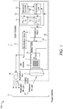
- FIG. 1 is a schematic block diagram of a three-dimensional (3D) depth camera system 100 according to one or more embodiments.
- the 3D depth camera system 100 includes a 3D depth camera 1 and an object 2.
- the object 2 may be one or more objects that make up a 3D scene for imaging.
- the 3D depth camera system 100 uses a ToF-based 3DI sensor concept, using indirect depth measurement with continuously modulated illumination signals sourcing an illumination unit, and a modulated sensor core, where on pixel-basis received light is demodulated by a pixel modulation signal.
- the 3D depth camera 1 is an image sensor that includes a sensor chip 3 comprising various components for performing depth measurement, an illumination unit 4, and imaging optics 5 (e.g., a lens).
- the illumination unit 4 may be an illumination source such as a such as a light emitting diode (LED) or a vertical-cavity surface-emitting laser (VCSEL) configured to emit a modulated light signal (e.g., modulated IR light), or any other suitable light source configured to emit a modulated illumination signal (e.g., modulated IR light or light signal).
- a modulated light signal e.g., modulated IR light
- any other suitable light source configured to emit a modulated illumination signal (e.g., modulated IR light or light signal).
- the illumination unit 4 may be configured to emit the modulated IR light towards the object 2, and the imaging optics 5 (e.g., a lens) may be configured to receive reflected modulated IR light that is reflected from the surface of the object 2.
- the imaging optics 5 e.g., a lens
- the terms "light signal”, “IR light”, and “illumination signal” may be used interchangeably herein.
- the illumination unit 4 may be further configured to emit the modulated IR light towards the object 2 using illumination optics (e.g., a lens or a diffractive optical element (DOE)).
- illumination optics e.g., a lens or a diffractive optical element (DOE)
- DOE diffractive optical element
- the imaging optics 5 which may be an imaging lens system or objective including one or more lenses or DOEs, is configured to receive reflected IR light that is reflected from object 2 (i.e., objects of a 3D scene). The reflected light is directed by the imaging optics 5 at a pixel array 6 of a sensor core 7.
- the sensor chip 3 includes the sensor core 7, which includes pixel array 6, an illumination driver 8, a modulation driver 9, and a control unit 10.
- the control unit includes two phase lock loop (PLL) circuits 11 and 12, a sequence controller 13, and a processing unit 14 that includes a binning module that is configured to increase the resolution of a resulting image by using pixel interpolation.
- the binning module is a circuit comprising entirely of hardware (e.g., logic circuitry) with no software or program code implemented by a processor being involved.
- a plurality of N readout channels 16 is used to couple the processing unit 14 to the pixel array 6 in order to read out electrical signals generated by the pixels.
- the sensor core 7 includes a multiplexer 15 that couples a pixel or a group of pixels of the pixel array to a corresponding readout channel that is assigned thereto.
- the sequence controller 13 is configured to change the pixel assignments to the readout channels 16 so that different pixels can be read out at different times by different readout channels 16. This helps to reduce the complexity of the readout circuit needed to readout the full pixel array.
- Each readout channel is coupled to a corresponding ADC at the processing unit 14, where each ADC is configured to receive electrical signals from the pixel or group of pixels that is coupled to the assigned readout channel.
- the PLL circuits 11 and 12, together, may form a modulator to modulate one or more driver signals.
- a first PLL 11 may be configured to control a modulation signal f Illu via the illumination driver 8 and a second PLL 12 may be configured control a modulation signal f mod via the modulation driver 9.
- the illumination driver 8 is configured to generate the illumination modulation signal f Illu having a first modulation frequency.
- the modulation driver 9 is configured to generate the sensor core (pixel) modulation signal f mod having a second modulation frequency.
- the PLLs 11 and 12 are configured such that the first and the second modulation frequencies may have a predetermined frequency difference greater than zero for at least a portion of the image acquisition time for each of the image acquisitions.
- the 3D depth camera 1 is configured to emit modulated IR light and measure the time the IR signal takes to travel from the depth camera 1 to the 3D scene 2 and back again.
- the elapsed time referred to as a "time-of-flight”
- the 3D depth camera 1 may be a continuous modulation ToF camera that measures the time-of-flight by using or determining a phase difference between the reflected modulated light and the modulation signal f mod .
- a phase difference can be translated to a distance based on the known frequency difference and an image acquisition time.
- a depth (distance) to the object can be determined from the phase difference information determined upon receipt of the reflected modulated light.
- the predetermined frequency difference may be set to be greater than zero for all or part of an integration time, all or part of a waiting time, or for all or part of an image acquisition time for each of a multiple image acquisitions taken at different image acquisition times.
- the frequencies of the modulation signals f mod and f Illu may be equal such that there is no frequency difference therebetween.
- the illumination driver 8 may be configured to receive a control signal from the first PLL 11, and output the modulation signal f Illu to the illumination unit 4 according to the control signal.
- the illumination unit 4 then generates a modulated light signal based on the illumination modulation signal f Illu .
- the modulation driver 9 may be configured to receive a control signal from the second PLL 12, and output the sensor core modulation signal f mod to a pixel array 6 of a sensor core 7 according to the control signal. While not shown, the modulation driver 9 may generate a plurality of modulation signals f mod that are received by the sensor core 7, each with a same modulation frequency and phase, to control the modulation frequency of the ToF pixels of the pixel array 6. Thus, when modulation signal f mod is referenced herein, it will be understood that this may include one or more signals with the same modulation frequency and phase for modulating the pixels of the pixel array 6.
- the pixel array 6 may be a 224x172 pixel matrix, but is not limited thereto.
- the pixel array 6 may be configured to receive the reflected IR signal from the imaging optics 5 and demodulate the reflected IR signal using the modulation signal f mod such that a phase difference (i.e., phase shift) between the modulated (reflected) illumination signal and the modulated pixel array 6 (e.g., signal f mod ) may be detected and measured.
- the pixel array 6 may be configured to directly demodulate the reflected light.
- the sensor core 7 includes the pixel array 6 modulated by the pixel modulation signal f mod , and a pixel of the pixel array 6 is configured to receive the modulated light signal reflected from object 2 as a reflected modulated light signal.
- the pixel of the pixel array 6 is further configured to demodulate the reflected modulated light signal using the pixel modulation signal f mod during an image acquisition to generate a measurement signal.
- the pixel is configured to generate a plurality of measurement signals based on a plurality of image acquisitions taken at different image acquisition times. Each pixel or a subset of pixels of the pixel array 6 may perform a similar process.
- the processing unit 14 may be configured to receive the plurality of measurement signals from each pixel (e.g., a plurality of measurement signals from each pixel) and calculate the depth of the object 2 on a pixel-by-pixel basis based on the plurality of measurement signals using phase difference information embedded in each measurement signal.
- the processing unit 14 may calculate an absolute phase difference based on the phase difference values associated with the measurement signals for each pixel, and translate the absolute phase difference into depth (distance) information.
- a 3D image of the object 2 can be generated, output, and/or displayed.
- the sequence controller 13 may include one or more processors and a clock source, and may be configured to control each of the PLLs 11 and 12. That is, the sequence controller 13 may be configured to control the modulation frequencies implemented by the PLLs 11 and 12 for controlling the two modulation signals f mod and f Illu and the frequency difference therebetween.
- the sequence controller 13 may be an internal controller logic with which the processing unit 14 can communicate with or through which the processing unit 14 may parametrize the depth camera 1 in order to control one or more of the pixel modulation and illumination modulation frequencies of f mod and f Illu , respectively, the duration and timing of introducing the frequency difference during each image acquisition provided by the PLLs 11 and 12, or the definition of an image sequence having defined frame rate.
- the first PLL circuit 11 and the second PLL circuit 12 may be coupled to each other such that they share a common clock source (e.g., provided by the sequence controller 13).
- a common clock source e.g., provided by the sequence controller 13.
- the two frequencies of the illumination modulation signal f Illu and the pixel modulation signal f mod are coupled to each other and can be derived from the same clock frequency.
- the frequency difference is greater than zero, it can be ensured that the phase difference between the modulation signals f mod and f Illu grows continuously and linearly over time in a consistent and expected manner.
- there is no frequency difference it can be ensured that the phase difference between the modulation signals f mod and f Illu does not change over time and remains constant.
- these two PLLs 11 and 12 may be programmed by the sequence controller 13 such that they differ slightly in frequency (e.g., a frequency difference 1Hz or 0.1Hz for modulation frequency of 80MHz for example).
- a synchronous start of the two PLLs 11 and 12 for sensor pixel modulation and illumination signal modulation can be achieved to start at phase difference of 0°, with a constant and continuously growing phase difference between the two modulation signals f Illu and f mod for at least part of an image acquisition time. That is, the frequency difference between the two modulation signals f Illu and f mod introduces a linear phase shift growing linearly with time. In principal, also a phase differences of greater than 360° can be used (phase ambiguity).
- phase differences of greater than 360° can be used (phase ambiguity).
- the phase difference may also set by the sequence controller 13 to be constant for at least part of an image acquisition by setting the frequency of the illumination modulation signal f Illu to be the same as the frequency of the pixel modulation signal f mod .
- the frequency difference is equal to zero (i.e., there is no frequency difference) and the phase difference between the modulation signals f mod and f Illu does not change over time.
- This programing of the set frequency difference allows a precisely controllable and, if wanted, continuously changeable phase difference between pixel modulation signal f mod and the illumination modulation signal f Illu for the 3DI sensor. At other times, there may be no frequency difference, which provides a constant, unchanging phase difference for a certain period of time during an image acquisition time.
- a combined PLL or modulator structure may be implemented where the two different frequencies can be obtained.
- a combined PLL structure may be implemented where the two different frequencies of the modulation signals f mod and f Illu are obtained.
- the combined PLL structure may be a dedicated PLL circuit enabling output of two stable signals with coupled frequencies.
- Additional embodiments herein are directed to using the binning module of the sensor chip 3 (i.e., of the image sensor 1) to increase the resolution of the resulting image by using pixel interpolation, and is applicable independent of the initial image sensor resolution defined by the pixel array 6.
- the binning module consisting only of hardware to perform the pixel interpolation, and thereby produce interpolated pixels (i.e., virtual pixels)
- the computational load on the application processor may be reduced and the memory requirements may be relaxed.
- the pixels resulting from the binning operation can be regarded as a single pixel with the area equal to the combined areas of the binned pixel. This means that the binned pixels offer much better sensitivity and lower noise, which in turn provides a sub-image with improved dynamic range and lower noise.
- This sub-image can be used as a reference image for making pixel validity/confidence decisions for the composing pixels in post processing. The net result would be increasing the resolution (up to 3 times) of the raw data, with the added benefit of an embedded image with higher confidence and improved signal-to-noise ratio (SNR).
- SNR signal-to-noise ratio
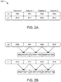
- FIGS. 2A-2C illustrate a pixel interpolation method according to one or more embodiments.
- FIG. 2A illustrates a 2x4 pixel array 200 comprising two pixel lines L0 and L1, also referred to a pixel rows, and N pixel columns, where N is equal to four in this example.
- Each pixel P is identified in a matrix format representative of its pixel line and pixel row.
- the pixel array 200 is representative of a simplified version of pixel array 6.
- each pixel P is an "actual",”real", or “physical” pixel configured to detect light and generate an electrical signal in response thereto.
- Binning in a "1x2 way” corresponds to averaging two adjacent pixels, real or virtual, located in a same pixel line but in different pixel columns.
- binning in a "2x1 way” corresponds to averaging two adjacent pixels, real or virtual, located in a same pixel column but in different pixel lines.
- the binning module is configured to bin the pixels of the first line L0 in a 1x2 way, producing one binned pixel B for every two actual pixels.
- the binned pixels B may also be referred to as virtual pixels.
- the binned pixels B are then inserted in between its parent pixels (i.e., those pixels used to generate the binned pixel data).
- binned pixel B00 is inserted between its parent pixels P00 and P01 in an image line of an image structure.
- the binning module is configured to add the pixel data (e.g., pixel values) of two adjacent pixels P, calculate average data (e.g., an average value) of from the sum, and store the average data as binned pixel data (e.g., a binned pixel value) of a binned pixel B.
- pixel data e.g., pixel values
- average data e.g., an average value
- pixels P00 and P01 are binned (i.e., added and averaged) to derive binned pixel data for binned pixel B00; pixels P01 and P02 are binned (i.e., added and averaged) to derive binned pixel data for binned pixel B01; and pixels P02 and P03 are binned (i.e., added and averaged) to derive binned pixel data for binned pixel B02.
- the same procedure is repeated for the pixels in line L01 to produce binned pixels B10, B11, and B12.
- each new line of pixels L0' and L1' includes an arrangement of interleaved actual pixel data and binned pixel data (e.g., interleaved actual pixel values and binned pixel values).
- the new line of pixels L0' and L1 may be referred to as interleaved pixel lines, and the pixel array can be said to include virtual pixel columns.
- the next step, illustrated in FIG. 2C is for the binning module to perform the same operation, but on the pixels between the two new lines in a 2x1 way, forming a third line L01, which consist only of averaged pixels (i.e., of binned pixels BB).
- the averaging operation is performed on adjacent pixels in the same pixel column, including the virtual pixel columns interposed between real pixel columns.
- the first pixels of new lines L0' and L1' are averaged together to generate a binned pixel BB(P00;P01); the second pixels of new lines L0' and L1' are averaged together to generate a binned pixel BB(B00;B10); the third pixels of new lines L0' and L1' are averaged together to generate a binned pixel BB(P01;P10); the fourth pixels of new lines L0' and L1' are averaged together to generate a binned pixel BB(B01;B11); the fifth pixels of new lines L0' and L1' are averaged together to generate a binned pixel BB(P02;P12); and so on.
- a new line L01 i.e., a virtual pixel line
- FIG. 2D illustrates a pixel structure of a final image 201 as a result of the pixel interpolation performed by the binning module.
- the virtual pixel line L01 is inserted in an image structure or memory structure between interleaved pixel lines L0' and L1'.
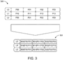
- FIG. 3 illustrates a pixel interpolation method according to one or more embodiments.
- a pixel array 300 representative of a simplified version of pixel array 6 and including three pixel lines L0, L1, and L2 and N pixel columns, where N is equal to four in this example.
- each pixel line is used to generate a virtual line of binned pixels.
- each new virtual line of binned pixels is used to replace their respective parent pixel lines in the image structure 301.
- virtual pixel line L0' replaces pixel line L0 in the image structure
- virtual pixel line L1' replaces pixel line L1 in the image structure
- virtual pixel line L2' replaces pixel line L2 in the image structure to generate a final image 301.
- the newly assembled pixel lines are output by an output circuit as image lines of the image structure.
- the final image structure 301 may be output by the output circuit as image lines that are arranged according to a sequence dictated by the image structure.
- a memory controller may be configured to allocate the newly assembled pixel lines to appropriate image lines or memory lines.
- the binning module is configured to perform sliding 2x1 interpolation. As such, the pixels of every line are binned in a 2x1 way, producing one binned pixel for every two real pixels, which results in an image where every pixel, being a binned pixel, has a reduced noise level. Reduced pixel noise would allow for certain reduction in the required illumination power but preserve the performance of the image sensor.
- FIG. 3 illustrates a pixel interpolation method according to one or more embodiments in which noise reduction is combined with upscaling the resolution.
- FIG. 4 illustrates a pixel array 300 representative of a simplified version of pixel array 6 and including three pixel lines L0, L1, and L2 and N pixel columns, where N is equal to four in this example.
- each pixel line L0, L1, and L2 of the pixel array 300 are individually used to create new virtual pixel lines L0', L1', and L'2.
- the binning module is configured to bin the pixels of the first line L0 in a 1x2 way, producing one binned pixel B for every two actual pixels.
- pixels P00 and P01 are binned (i.e., added and averaged) to derive binned pixel data for binned pixel B00; pixels P01 and P02 are binned (i.e., added and averaged) to derive binned pixel data for binned pixel B01; and pixels P02 and P03 are binned (i.e., added and averaged) to derive binned pixel data for binned pixel B02.
- the same procedure is repeated for the pixels in line L01 to produce binned pixels B10, B11, and B12, and for the pixels in line L02 to produce binned pixels B20, B21, and B22.
- Each new virtual pixel lines L0', L1', and L'2 consists only of averaged pixels (i.e., binned pixels).
- actual pixel lines L0 and L1 are used to create a new virtual pixel line L01
- actual pixel lines L2 and L2 are used to create a new virtual pixel line L02.
- each adjacent pair of real pixel lines of the pixel array are used to generate a new virtual pixel line.
- the averaging operation is performed on adjacent pixels in the same pixel column.
- the averaging is performed on the pixels between the two lines in a 2x1 way, forming another pixel line, which consists only of averaged pixels.
- the final image structure 302 is assembled by an output circuit configured to assign newly formed pixel lines to appropriate image lines or memory lines according to the final image structure 302.
- virtual pixels lines are arranged in the following sequence: L0, L01, L1, L02, and L2 such that the virtual pixel lines formed from a single actual pixel line in a 1x2 way are interleaved with those virtual pixel lines formed from two actual pixel lines in a 2x1 way.
- the virtual pixels lines are arranged in the following sequence: L0, L01, L1, L02, and L2 such that the virtual pixel lines formed from averaging adjacent pixels from a same actual pixel line are interleaved with those virtual pixel lines formed from averaging pixels in adjacent pixel lines.
- a virtual pixel line generated in the 2x1 way from two parent pixel lines is inserted in an image structure between the virtual pixel lines generated in the 1x2 way from those parent pixel lines.
- the SNR may be improved by reducing pixel noise. This is achieved, by the binning module performing a sliding 2x1 interpolation. Adding the possibility to do the same in vertical direction - between pixel lines, also enhances the resolution. As can be seen from the final image structure 302, this requires extra image lines or memory lines to accommodate virtual pixel lines L01, L02, and so forth. This can be enhanced further by doubling the number of ADCs and reading two lines in parallel. The reduced pixel noise would allow for certain reduction in the required illumination power but preserve the performance, and also there is an added benefit from the improved resolution.
- FIG. 5 shows a schematic block diagram of a binning pipeline 500 according to one or more embodiments.
- the binning pipeline 500 is integrated on the sensor chip 3 of the image sensor 1.
- the binning pipeline includes pixels of the pixel array 6, a multiplexer 15, readout channels 51-0, 51-1, 51-2, and 51-3, each selectively coupled by the multiplexer 15 to an assigned pixel of the pixel array 6, ADCs 53-0, 53-1, 53-2, or 53-3 that are each coupled to a corresponding readout channel of readout channels 51-0, 51-1, 51-2, and 51-3, a binning module 501, and an output circuit 502 coupled to output channels 52-0, 52-1, and 52-2 of the binning module 501.
- the output circuit 502 is configured to receive actual pixel values from the ADCs and virtual pixel values form the binning module 501 and output a total number of pixel values according to an image structure.
- the image structure may have more pixels than the pixel array 6.
- the output circuit 502 may include a memory controller 503 coupled to output channels 52-0, 52-1, and 52-2 of the binning module 501, and an output circuit memory 504 coupled to the memory controller 503.
- the output circuit 502 may include a first in, first out (FIFO) circuit that receives lines of pixel values and outputs the lines of pixel values as image lines of an image structure on a FIFO basis.
- FIFO first in, first out
- the pixels shown include only a partial pixel line of the pixel array 6.
- the pixels include Pixel[i+0], Pixel[i+1], Pixel[i+2], and Pixel[i+3] that are located in row "i" and columns 0-3 of the pixel array 6.
- Each pixel generates an analog electrical signal (i.e., an analog sensor signal) in response to receiving light and is coupled to a corresponding ADC 53-0, 53-1, 53-2, or 53-3.
- the ADCs may be part of the binning module 501, or interposed between the pixels and the binning module 501.
- Each ADC converts a respective analog electrical signal into digital pixel data, which may also be referred to as a digital sensor signal, a digital measurement signal, or actual pixel data.
- the output circuit 502 may be configured to receive the digital sensor signals as pixel data (i.e., pixel values) and output the pixel data as image lines of an image structure.
- the memory controller 503 may be configured to receive the digital sensor signals as pixel data (i.e., pixel values) and store the pixel data in appropriate memory lines of memory 504 corresponding to an image structure.
- the binning module 501 further includes multiple arithmetic logic units (ALUs), each being configured to receive a pair of digital sensor signals from the ADCs, the pair of digital sensor signals in this case corresponding to two adjacent pixels in the same pixel line (e.g., to perform binning in a "1x2 way").
- ALUs arithmetic logic units
- additional ALUs may be provided that are configured to receive digital sensor signals from a pair of adjacent pixels from the same pixel column (e.g., to perform binning in a "2x1 way").
- each ALU is a digital electronic circuit that comprises averaging logic configured to receive two digital sensor signals corresponding to a pair of adjacent pixels, and generate average (i.e., binned) data as a result of an averaging operation.
- the pixel data whether actual or binned, may also be referred to as pixel values.
- ALU0 is configured to receive digital sensor signals corresponding to Pixel[i+0] and Pixel[i+1], and generate binned pixel data as result R0.
- ALU1 is configured to receive digital sensor signals corresponding to Pixel[i+1] and Pixel[i+2], and generate binned pixel data as result R1.
- ALU2 is configured to receive digital sensor signals corresponding to Pixel[i+2] and Pixel[i+3], and generate binned pixel data as result R3.
- the binning module 501 may further includes data buffers 54-0, 54-1, and 54-2 configured to store the results R0, R1, and R2, respectively, as binned data.
- data buffer 54-0 stores the binned pixel data of result R0 as WDATA[i+0]
- data buffer 54-1 stores the binned pixel data of result R1 as WDATA[i+1]
- data buffer 54-2 stores the binned pixel data of result R2 as WDATA[i+2].
- the data buffers 54-0, 54-1, and 54-2 are representative of virtual pixels.
- the binning module 501 may be further configured to output the binned data WDATA[i+0], WDATA[i+1], and WDATA[i+2] via output channels 52-0, 52-1, and 52-2 to the output circuit 502.
- the output circuit 502 is configured to receive the binned data and arrange the binned data into image lines according to an image structure.
- the memory controller 503 may store the binned data in memory lines of memory 503 corresponding to the image structure.
- the binning module 501 may further include another stage of ALUs coupled to at least one of the data buffers 54-0, 54-1, and 54-2 for receiving binned pixel data in order to perform a second stage of averaging operations.
- a second stage ALU would be coupled to the data buffer storing binned pixel data B00 and to the data buffer storing binned pixel data B10 in order to generate binned pixel data BB(B00; B10) (i.e., an average of binned pixel data B00 and B10).
- Another second stage ALU would be coupled to the data buffer storing binned pixel data B01 and to the data buffer storing binned pixel data B11 in order to generate binned pixel data BB(B01; B11) (i.e., an average of binned pixel data B01 and B11).
- a pair of adjacent pixels to which an ALU is coupled may include two real pixels, two virtual pixels, or a mix of one real pixel and one virtual pixel based on a desired averaging operation, and the ALUs may be arranged in multiple stages in order to achieve the desired resolution and/or noise reduction.
- the output circuit 502 may be further configured to read out the image data on an image line-by-image line basis a processor for further data processing, including object detection, object classification, etc.
- the memory controller 503 may be configured to read out from memory 503 image lines according to memory lines, and output the image data to a processor for further data processing, including object detection, object classification, etc.
- the binned image can provide a minimum amount of 3D points in adverse conditions, which can help the system to remain functional even at the cost of decreased performance.
- the enhanced resolution of the image can be useful in improving the detection rate of object detection and classification algorithms used by the system controller 23. Even though the interpolated resolution does not add new data, it can improve the robustness of the existing data and help on algorithm level to make a decision based on the increased pixel number - the increased pixel number can help in object detection and classification, although based on interpolated data.
- the interpolation may be a solution to closing the gap to Video Graphics Array (VGA) resolution and may improve object separation due to the enhanced resolution.
- VGA Video Graphics Array
- the concept is to rework the binning module and the memory structure, to enable the imager to generate an interpolated image, which contains the real and the interpolated (virtual) pixels.
- the binned pixels may also have an advantage of better SNR and dynamic range, so the expectation is that the end result will be an increased number of valid 3D points.
- aspects have been described in the context of an apparatus, it is clear that these aspects also represent a description of the corresponding method, where a block or device corresponds to a method step or a feature of a method step. Analogously, aspects described in the context of a method step also represent a description of a corresponding block or item or feature of a corresponding apparatus.
- Some or all of the method steps may be executed by (or using) a hardware apparatus, like for example, a microprocessor, a programmable computer, or an electronic circuit. In some embodiments, some one or more of the method steps may be executed by such an apparatus.
- embodiments provided herein can be implemented in hardware or in software.
- the implementation can be performed using a digital storage medium, for example a floppy disk, a DVD, a Blue-Ray, a CD, a ROM, a PROM, an EPROM, an EEPROM or a FLASH memory, having electronically readable control signals stored thereon, which cooperate (or are capable of cooperating) with a programmable computer system such that the respective method is performed. Therefore, the digital storage medium may be computer readable.
- processors such as one or more central processing units (CPU), digital signal processors (DSPs), general purpose microprocessors, application specific integrated circuits (ASICs), field programmable logic arrays (FPGAs), or other equivalent integrated or discrete logic circuitry.
- CPU central processing units
- DSP digital signal processors
- ASIC application specific integrated circuits
- FPGA field programmable logic arrays
- processors such as one or more central processing units (CPU), digital signal processors (DSPs), general purpose microprocessors, application specific integrated circuits (ASICs), field programmable logic arrays (FPGAs), or other equivalent integrated or discrete logic circuitry.
- CPU central processing units
- DSPs digital signal processors
- ASICs application specific integrated circuits
- FPGAs field programmable logic arrays
Landscapes
- Engineering & Computer Science (AREA)
- Physics & Mathematics (AREA)
- Multimedia (AREA)
- Signal Processing (AREA)
- Electromagnetism (AREA)
- Computer Networks & Wireless Communication (AREA)
- General Physics & Mathematics (AREA)
- Radar, Positioning & Navigation (AREA)
- Remote Sensing (AREA)
- Transforming Light Signals Into Electric Signals (AREA)
- Optical Radar Systems And Details Thereof (AREA)
- Image Processing (AREA)
Applications Claiming Priority (1)
| Application Number | Priority Date | Filing Date | Title |
|---|---|---|---|
| US16/449,665 US11570424B2 (en) | 2019-06-24 | 2019-06-24 | Time-of-flight image sensor resolution enhancement and increased data robustness using a binning module |
Publications (1)
| Publication Number | Publication Date |
|---|---|
| EP3757618A1 true EP3757618A1 (de) | 2020-12-30 |
Family
ID=71120029
Family Applications (1)
| Application Number | Title | Priority Date | Filing Date |
|---|---|---|---|
| EP20181302.9A Pending EP3757618A1 (de) | 2019-06-24 | 2020-06-22 | Laufzeitbildsensorauflösungsverzauberung und erhöhte datenrobustheit unter verwendung eines binning-moduls |
Country Status (3)
| Country | Link |
|---|---|
| US (2) | US11570424B2 (de) |
| EP (1) | EP3757618A1 (de) |
| CN (1) | CN112135114B (de) |
Families Citing this family (8)
| Publication number | Priority date | Publication date | Assignee | Title |
|---|---|---|---|---|
| US11570424B2 (en) | 2019-06-24 | 2023-01-31 | Infineon Technologies Ag | Time-of-flight image sensor resolution enhancement and increased data robustness using a binning module |
| TWI853067B (zh) * | 2019-08-21 | 2024-08-21 | 荷蘭商露明控股公司 | 紅外線成像組件、使用一紅外線成像組件來產生一場景之一深度圖之方法及相機 |
| US11431936B2 (en) * | 2020-04-21 | 2022-08-30 | Omnivision Technologies, Inc. | Image sensor with shared gray code generator and parallel column arithmetic logic units |
| US11721031B2 (en) * | 2020-10-28 | 2023-08-08 | Stmicroelectronics (Research & Development) Limited | Scalable depth sensor |
| US20220260679A1 (en) * | 2021-02-17 | 2022-08-18 | Continental Automotive Systems, Inc. | Lidar system that detects modulated light |
| EP4141488A1 (de) * | 2021-08-31 | 2023-03-01 | Infineon Technologies AG | Verfahren zur pixel-binning in einem flugzeitsensor, schaltvorrichtung für einen flugzeitsensor und computerprogramm |
| US11778337B2 (en) * | 2021-11-09 | 2023-10-03 | Samsung Electronics Co., Ltd. | Image sensor and method for sensing image |
| US20240427018A1 (en) * | 2023-06-23 | 2024-12-26 | Qualcomm Incorporated | Depth-event camera |
Citations (3)
| Publication number | Priority date | Publication date | Assignee | Title |
|---|---|---|---|---|
| US20110129123A1 (en) * | 2009-11-27 | 2011-06-02 | Ilia Ovsiannikov | Image sensors for sensing object distance information |
| US20180081043A1 (en) * | 2016-09-16 | 2018-03-22 | Analog Devices, Inc. | Interference handling in time-of-flight depth sensing |
| US20180295297A1 (en) * | 2015-03-10 | 2018-10-11 | Samsung Electronics Co., Ltd. | Image sensor, data processing system including the same |
Family Cites Families (15)
| Publication number | Priority date | Publication date | Assignee | Title |
|---|---|---|---|---|
| US5093721A (en) * | 1990-07-10 | 1992-03-03 | Zenith Electronics Corporation | Line interpolator with preservation of diagonal resolution |
| JP4077120B2 (ja) * | 1999-07-01 | 2008-04-16 | 富士フイルム株式会社 | 固体撮像装置および信号処理方法 |
| US7062013B2 (en) * | 2001-04-12 | 2006-06-13 | Jordan Valley Applied Radiation Ltd. | X-ray reflectometry of thin film layers with enhanced accuracy |
| US7379105B1 (en) * | 2002-06-18 | 2008-05-27 | Pixim, Inc. | Multi-standard video image capture device using a single CMOS image sensor |
| KR100707071B1 (ko) * | 2005-12-02 | 2007-04-13 | 매그나칩 반도체 유한회사 | 자동 블랙 레벨 보상 기능을 갖는 이미지 센서 및 자동블랙 레벨 보상방법 |
| US8629926B2 (en) * | 2011-11-04 | 2014-01-14 | Honeywell International, Inc. | Imaging apparatus comprising image sensor array having shared global shutter circuitry |
| US9971023B2 (en) | 2015-05-04 | 2018-05-15 | Infineon Technologies Ag | Systems and methods for time of flight measurement using a single exposure |
| US9921298B2 (en) * | 2015-07-20 | 2018-03-20 | Google Llc | Method and apparatus for increasing the resolution of a time of flight pixel array |
| EP3846449B1 (de) * | 2016-04-15 | 2024-11-06 | Sony Group Corporation | Festkörper-bildsensor, elektronisches gerät und steuerverfahren für einen festkörper-bildsensor |
| US9906717B1 (en) * | 2016-09-01 | 2018-02-27 | Infineon Technologies Ag | Method for generating a high-resolution depth image and an apparatus for generating a high-resolution depth image |
| CN106412407B (zh) * | 2016-11-29 | 2019-06-07 | Oppo广东移动通信有限公司 | 控制方法、控制装置及电子装置 |
| US10809128B2 (en) * | 2017-03-31 | 2020-10-20 | The Regents Of The University Of California | General noise suppression scheme with reference detection in optical heterodyne spectroscopy |
| KR102624984B1 (ko) * | 2018-03-21 | 2024-01-15 | 삼성전자주식회사 | ToF 센서와 이를 이용한 3차원 영상 장치 및 3차원 영상 장치의 구동 방법 |
| KR102606240B1 (ko) * | 2018-07-09 | 2023-11-24 | 삼성전자주식회사 | 멀티탭 픽셀을 포함하는 이미지 센서 |
| US11570424B2 (en) | 2019-06-24 | 2023-01-31 | Infineon Technologies Ag | Time-of-flight image sensor resolution enhancement and increased data robustness using a binning module |
-
2019
- 2019-06-24 US US16/449,665 patent/US11570424B2/en active Active
-
2020
- 2020-06-22 EP EP20181302.9A patent/EP3757618A1/de active Pending
- 2020-06-23 CN CN202010580907.5A patent/CN112135114B/zh active Active
-
2022
- 2022-12-08 US US18/063,188 patent/US11991341B2/en active Active
Patent Citations (3)
| Publication number | Priority date | Publication date | Assignee | Title |
|---|---|---|---|---|
| US20110129123A1 (en) * | 2009-11-27 | 2011-06-02 | Ilia Ovsiannikov | Image sensors for sensing object distance information |
| US20180295297A1 (en) * | 2015-03-10 | 2018-10-11 | Samsung Electronics Co., Ltd. | Image sensor, data processing system including the same |
| US20180081043A1 (en) * | 2016-09-16 | 2018-03-22 | Analog Devices, Inc. | Interference handling in time-of-flight depth sensing |
Also Published As
| Publication number | Publication date |
|---|---|
| US20200404246A1 (en) | 2020-12-24 |
| CN112135114A (zh) | 2020-12-25 |
| CN112135114B (zh) | 2025-01-17 |
| US20230108515A1 (en) | 2023-04-06 |
| US11991341B2 (en) | 2024-05-21 |
| US11570424B2 (en) | 2023-01-31 |
Similar Documents
| Publication | Publication Date | Title |
|---|---|---|
| US11991341B2 (en) | Time-of-flight image sensor resolution enhancement and increased data robustness using a binning module | |
| CN110596725B (zh) | 基于插值的飞行时间测量方法及测量系统 | |
| CN110133671B (zh) | 双频飞行时间三维图像传感器及测量对象深度的方法 | |
| CN110023785B (zh) | 距离测定装置 | |
| KR102904495B1 (ko) | 명확한 범위 토글링에 의해 비행 시간 시스템의 범위를 증가시키기 위한 방법 및 시스템 | |
| CN110596724B (zh) | 动态直方图绘制飞行时间距离测量方法及测量系统 | |
| JP6246131B2 (ja) | タイムオブフライト信号の処理における又はこれに関する改良 | |
| CN110596721A (zh) | 双重共享tdc电路的飞行时间距离测量系统及测量方法 | |
| CN110596723B (zh) | 动态直方图绘制飞行时间距离测量方法及测量系统 | |
| JP5918763B2 (ja) | 階層的な飛行時間(tof)システムのディエリアシング方法およびシステム | |
| CN110596722A (zh) | 直方图可调的飞行时间距离测量系统及测量方法 | |
| US8642938B2 (en) | Shared time of flight pixel | |
| US20200349728A1 (en) | Time-of-flight depth measurement using modulation frequency adjustment | |
| US11269065B2 (en) | Muilti-detector with interleaved photodetector arrays and analog readout circuits for lidar receiver | |
| CN112945221B (zh) | 相位角校正值计算装置和计算相位角校正值的方法 | |
| TWI898971B (zh) | 飛行時間感測系統中使用的圖像感測器 | |
| JP6261681B2 (ja) | タイムオブフライト信号の処理における又はこれに関する改良 | |
| WO2020214914A1 (en) | Single frame distance disambiguation | |
| WO2010139609A1 (en) | Method and device for acquiring a range image | |
| JP2006337286A (ja) | 形状計測装置 | |
| WO2011020921A1 (en) | Time-of-flight sensor | |
| JP4673674B2 (ja) | 形状測定装置 | |
| JP2006201037A (ja) | 形状測定装置 | |
| KR20240113225A (ko) | 거리 측정을 위한 장치 |
Legal Events
| Date | Code | Title | Description |
|---|---|---|---|
| PUAI | Public reference made under article 153(3) epc to a published international application that has entered the european phase |
Free format text: ORIGINAL CODE: 0009012 |
|
| STAA | Information on the status of an ep patent application or granted ep patent |
Free format text: STATUS: THE APPLICATION HAS BEEN PUBLISHED |
|
| AK | Designated contracting states |
Kind code of ref document: A1 Designated state(s): AL AT BE BG CH CY CZ DE DK EE ES FI FR GB GR HR HU IE IS IT LI LT LU LV MC MK MT NL NO PL PT RO RS SE SI SK SM TR |
|
| AX | Request for extension of the european patent |
Extension state: BA ME |
|
| STAA | Information on the status of an ep patent application or granted ep patent |
Free format text: STATUS: REQUEST FOR EXAMINATION WAS MADE |
|
| 17P | Request for examination filed |
Effective date: 20210616 |
|
| RBV | Designated contracting states (corrected) |
Designated state(s): AL AT BE BG CH CY CZ DE DK EE ES FI FR GB GR HR HU IE IS IT LI LT LU LV MC MK MT NL NO PL PT RO RS SE SI SK SM TR |
|
| STAA | Information on the status of an ep patent application or granted ep patent |
Free format text: STATUS: EXAMINATION IS IN PROGRESS |
|
| 17Q | First examination report despatched |
Effective date: 20240404 |