EP3754693A1 - Carrier lifespan measurement method and carrier lifespan measurement device - Google Patents
Carrier lifespan measurement method and carrier lifespan measurement device Download PDFInfo
- Publication number
- EP3754693A1 EP3754693A1 EP19754408.3A EP19754408A EP3754693A1 EP 3754693 A1 EP3754693 A1 EP 3754693A1 EP 19754408 A EP19754408 A EP 19754408A EP 3754693 A1 EP3754693 A1 EP 3754693A1
- Authority
- EP
- European Patent Office
- Prior art keywords
- light
- measurement
- measurement target
- target object
- carrier lifetime
- Prior art date
- Legal status (The legal status is an assumption and is not a legal conclusion. Google has not performed a legal analysis and makes no representation as to the accuracy of the status listed.)
- Granted
Links
Images




Classifications
-
- G—PHYSICS
- G01—MEASURING; TESTING
- G01N—INVESTIGATING OR ANALYSING MATERIALS BY DETERMINING THEIR CHEMICAL OR PHYSICAL PROPERTIES
- G01N21/00—Investigating or analysing materials by the use of optical means, i.e. using sub-millimetre waves, infrared, visible or ultraviolet light
- G01N21/84—Systems specially adapted for particular applications
- G01N21/88—Investigating the presence of flaws or contamination
- G01N21/95—Investigating the presence of flaws or contamination characterised by the material or shape of the object to be examined
- G01N21/9501—Semiconductor wafers
-
- G—PHYSICS
- G01—MEASURING; TESTING
- G01N—INVESTIGATING OR ANALYSING MATERIALS BY DETERMINING THEIR CHEMICAL OR PHYSICAL PROPERTIES
- G01N21/00—Investigating or analysing materials by the use of optical means, i.e. using sub-millimetre waves, infrared, visible or ultraviolet light
- G01N21/17—Systems in which incident light is modified in accordance with the properties of the material investigated
- G01N21/1717—Systems in which incident light is modified in accordance with the properties of the material investigated with a modulation of one or more physical properties of the sample during the optical investigation, e.g. electro-reflectance
-
- G—PHYSICS
- G01—MEASURING; TESTING
- G01N—INVESTIGATING OR ANALYSING MATERIALS BY DETERMINING THEIR CHEMICAL OR PHYSICAL PROPERTIES
- G01N21/00—Investigating or analysing materials by the use of optical means, i.e. using sub-millimetre waves, infrared, visible or ultraviolet light
- G01N21/84—Systems specially adapted for particular applications
- G01N21/88—Investigating the presence of flaws or contamination
- G01N21/95—Investigating the presence of flaws or contamination characterised by the material or shape of the object to be examined
- G01N21/9501—Semiconductor wafers
- G01N21/9505—Wafer internal defects, e.g. microcracks
-
- G—PHYSICS
- G01—MEASURING; TESTING
- G01R—MEASURING ELECTRIC VARIABLES; MEASURING MAGNETIC VARIABLES
- G01R31/00—Arrangements for testing electric properties; Arrangements for locating electric faults; Arrangements for electrical testing characterised by what is being tested not provided for elsewhere
- G01R31/26—Testing of individual semiconductor devices
- G01R31/2642—Testing semiconductor operation lifetime or reliability, e.g. by accelerated life tests
-
- H—ELECTRICITY
- H02—GENERATION; CONVERSION OR DISTRIBUTION OF ELECTRIC POWER
- H02S—GENERATION OF ELECTRIC POWER BY CONVERSION OF INFRARED RADIATION, VISIBLE LIGHT OR ULTRAVIOLET LIGHT, e.g. USING PHOTOVOLTAIC [PV] MODULES
- H02S50/00—Monitoring or testing of PV systems, e.g. load balancing or fault identification
- H02S50/10—Testing of PV devices, e.g. of PV modules or single PV cells
-
- G—PHYSICS
- G01—MEASURING; TESTING
- G01N—INVESTIGATING OR ANALYSING MATERIALS BY DETERMINING THEIR CHEMICAL OR PHYSICAL PROPERTIES
- G01N21/00—Investigating or analysing materials by the use of optical means, i.e. using sub-millimetre waves, infrared, visible or ultraviolet light
- G01N21/17—Systems in which incident light is modified in accordance with the properties of the material investigated
- G01N21/1717—Systems in which incident light is modified in accordance with the properties of the material investigated with a modulation of one or more physical properties of the sample during the optical investigation, e.g. electro-reflectance
- G01N2021/1719—Carrier modulation in semiconductors
-
- G—PHYSICS
- G01—MEASURING; TESTING
- G01N—INVESTIGATING OR ANALYSING MATERIALS BY DETERMINING THEIR CHEMICAL OR PHYSICAL PROPERTIES
- G01N21/00—Investigating or analysing materials by the use of optical means, i.e. using sub-millimetre waves, infrared, visible or ultraviolet light
- G01N21/17—Systems in which incident light is modified in accordance with the properties of the material investigated
- G01N21/1717—Systems in which incident light is modified in accordance with the properties of the material investigated with a modulation of one or more physical properties of the sample during the optical investigation, e.g. electro-reflectance
- G01N2021/1725—Modulation of properties by light, e.g. photoreflectance
-
- Y—GENERAL TAGGING OF NEW TECHNOLOGICAL DEVELOPMENTS; GENERAL TAGGING OF CROSS-SECTIONAL TECHNOLOGIES SPANNING OVER SEVERAL SECTIONS OF THE IPC; TECHNICAL SUBJECTS COVERED BY FORMER USPC CROSS-REFERENCE ART COLLECTIONS [XRACs] AND DIGESTS
- Y02—TECHNOLOGIES OR APPLICATIONS FOR MITIGATION OR ADAPTATION AGAINST CLIMATE CHANGE
- Y02E—REDUCTION OF GREENHOUSE GAS [GHG] EMISSIONS, RELATED TO ENERGY GENERATION, TRANSMISSION OR DISTRIBUTION
- Y02E10/00—Energy generation through renewable energy sources
- Y02E10/50—Photovoltaic [PV] energy
Definitions
- the present disclosure relates to a carrier lifetime measurement method and a carrier lifetime measurement device for measuring a lifetime of carriers in a measurement target object.
- a device for performing characteristic evaluation of a measurement target object such as a solar battery
- This device is configured to have a pumping light source irradiating a measurement target object with pulsed pumping light, a probe light source continuously irradiating the measurement target object with probe light, a photo detector detecting the probe light used for irradiating the measurement target object in real time, and a signal processing unit processing a signal output from the photo-detector. According to such a configuration, it is possible to measure circumstances of generation and extinction of carriers by measuring a change in carrier quantity over time.
- Patent Literature 1 Japanese Unexamined Patent Publication No. 2016-157780
- An embodiment aims to provide a carrier lifetime measurement method and a carrier lifetime measurement device capable of accurately measuring a lifetime of carriers in a measurement target object.
- a carrier lifetime measurement method for measuring a lifetime of carriers in a measurement target object.
- the carrier lifetime measurement method includes an irradiation step of irradiating the measurement target object with measurement light and stimulus light subjected to intensity modulation using a plurality of frequencies, an outputting step of outputting a detection signal by detecting an intensity of reflected light from the measurement target object or transmitted light through the measurement target object, and a generation step of detecting a phase delay of the detection signal with respect to a modulation signal including a frequency in association with a concentration of impurities in a measurement target region of the plurality of frequencies and generating image data indicating a distribution of lifetimes of carriers in the measurement target object on the basis of the phase delay.
- a carrier lifetime measurement device for measuring a lifetime of carriers in a measurement target object.
- the carrier lifetime measurement device includes a first light source configured to generate measurement light, a second light source configured to generate stimulus light, a modulation unit configured to perform intensity modulation of the stimulus light using a plurality of frequencies, a photo detector configured to output a detection signal by detecting an intensity of reflected light from the measurement target object or transmitted light through the measurement target object, an optical system configured to guide the measurement light and the stimulus light subjected to intensity modulation toward the measurement target object and to guide reflected light from the measurement target object or transmitted light through the measurement target object toward the photo detector, and an analysis unit configured detect a phase delay of the detection signal with respect to a modulation signal including a frequency in association with a concentration of impurities in a measurement target region of the plurality of frequencies, and to generate image data indicating a distribution of lifetimes of carriers in the measurement target object on the basis of the phase delay.
- a measurement target object is irradiated with measurement light and stimulus light subjected to intensity modulation using a plurality of frequencies, and an intensity of reflected light from the measurement target object or transmitted light through the measurement target object is detected.
- image data indicating a distribution of lifetimes of carriers is generated on the basis of an output detection signal.
- a phase delay of a detection signal with respect to a modulation signal including a frequency in association with a concentration of impurities in a measurement target region is detected, and a distribution of lifetimes of carriers is measured on the basis of the phase delay. In this manner, even when a concentration of impurities in a measurement target region changes in a variety of ways, it is possible to accurately measure a distribution of lifetimes of carriers.
- FIG. 1 is a view of a schematic configuration of a carrier lifetime measurement device 1 according to the embodiment.
- the carrier lifetime measurement device 1 shown in FIG. 1 is a device for measuring a lifetime of carriers in a device under test (DUT) 10 serving as a measurement target object such as a semiconductor device by performing optical measurement targeting the DUT 10.
- a measurement target of the carrier lifetime measurement device 1 a semiconductor device in which a circuit element such as a transistor is formed on a semiconductor substrate is favorably used. More favorably, a region which is estimated to include a defective part using a default defect analyzing method (an analyzing method such as light emission analysis, heat generation analysis, or optical beam induced resistance change (OBIRCH) analysis) in advance may be adopted as a measurement target.
- a default defect analyzing method an analyzing method such as light emission analysis, heat generation analysis, or optical beam induced resistance change (OBIRCH) analysis
- This carrier lifetime measurement device 1 is configured to include a stage 3 on which the DUT 10 is disposed; a light irradiation/light guiding system (optical system) 5 which guides light toward the DUT 10, irradiates the DUT 10 with the light, and guides reflected light from the DUT 10; and a control system 7 which controls the light irradiation/light guiding system 5, detects reflected light from the DUT 10, and performs processing of the reflected light.
- the stage 3 is a support unit supporting the DUT 10 so that the DUT 10 faces the light irradiation/light guiding system 5.
- the stage 3 may be equipped with a movement mechanism which can move the DUT 10 relatively to the light irradiation/light guiding system 5.
- a traveling path of light is indicated by a dashed-dotted line
- a transmission path of a control signal and transmission paths of a detection signal and processing data are indicated by solid arrows.
- the light irradiation/light guiding system 5 includes a light source (first light source) 9a, a light source (second light source) 9b, collimators 11a and 11b, a dichroic mirror 13, a polarization beam splitter 15, a quarter-wavelength plate 17, a galvanometer mirror 19, a pupil projection lens 21, an object lens 23, an optical filter 25, and a collimator 27.
- the light source 9a generates and emits light as measurement light (probe light) that has a wavelength and an intensity suitable for detecting optical characteristics which change in association with the concentration of impurities in the DUT 10.
- the light source 9b generates and emits light as stimulus light (pumping light) that includes a wavelength component which is partially absorbed in the DUT 10.
- the light source 9b is set to generate stimulus light including a wavelength associated with an energy higher than a band-gap energy of a semiconductor which is a material for a substrate configuring the DUT 10.
- this light source 9b is configured to be able to generate stimulus light subjected to intensity modulation on the basis of an electrical signal from the outside.
- the light source 9a and the light source 9b may be coherent light sources such as semiconductor lasers or may be incoherent light sources such as super luminescent diodes (SLDs).
- the collimators 11a and 11b respectively collimate rays of light emitted from the light sources 9a and 9b, and the dichroic mirror 13 coaxially synthesizes measurement light and stimulus light which have been collimated and outputs the coaxially synthesized light toward the polarization beam splitter 15.
- the polarization beam splitter 15 allows linearly polarized components of measurement light and stimulus light which have been synthesized to be transmitted therethrough, and the quarter-wavelength plate 17 changes polarization states of the measurement light and the stimulus light which have been transmitted through the polarization beam splitter 15 and sets the polarization states of the measurement light and the stimulus light in circular polarization.
- the galvanometer mirror 19 performs scanning with measurement light and stimulus light in circular polarization and outputs the measurement light and the stimulus light
- the pupil projection lens 21 relays pupils of measurement light and stimulus light output from the galvanometer mirror 19 to a pupil of the object lens 23 from the galvanometer mirror 19.
- the object lens 23 collects measurement light and stimulus light on the DUT 10. According to such a configuration, a desired position on the DUT 10 can be scanned and irradiated with measurement light and stimulus light which have been synthesized.
- the carrier lifetime measurement device 1 may be configured to be able to perform scanning with measurement light and stimulus light targeting a range which the galvanometer mirror 19 cannot cover by moving the stage 3.
- reflected light from the DUT 10 can be guided to the quarter-wavelength plate 17 in a manner of being coaxial with measurement light and stimulus light, and the polarization state of reflected light can be changed from circular polarization to linear polarization by the quarter-wavelength plate 17.
- linearly polarized reflected light is reflected toward the optical filter 25 and the collimator 27 by the polarization beam splitter 15.
- the optical filter 25 is configured to allow only the same wavelength component as that of measurement light of reflected light to be transmitted therethrough toward the collimator 27 and to block the same wavelength component as that of stimulus light of reflected light.
- the collimator 27 collimates reflected light and outputs the reflected light toward the control system 7 via an optical fiber or the like.
- the control system 7 includes a photo detector 29, an amplifier 31, a modulation signal source (modulation unit) 33, a network analyzer 35 (analysis unit), a controller (analysis unit) 37, and a laser scanning controller 39.
- the photo detector 29 is a photo detection element such as a photodiode (PD), an avalanche photodiode (APD), or a photomultiplier tube, which receives reflected light guided by the light irradiation/light guiding system 5, detects the intensity of the reflected light, and outputs a detection signal.
- the amplifier 31 amplifies a detection signal output from the photo detector 29 and outputs an amplified result to the network analyzer 35.
- the modulation signal source 33 generates an electrical signal (modulation signal) having a waveform set by the controller 37 and controls the light source 9b so that stimulus light is subjected to intensity modulation on the basis of the electrical signal.
- the modulation signal source 33 generates an electrical signal having rectangular waves of a set repetition frequency (default frequency) and controls the light source 9b on the basis of the electrical signal.
- the modulation signal source 33 also has a function of repetitively generating an electrical signal having rectangular waves of a plurality of repetition frequencies. Stimulus light subjected to intensity modulation due to each of rectangular waves of repetition frequencies includes components of a plurality of frequencies including the repetition frequencies and frequencies having higher harmonic waves thereof.
- the network analyzer 35 extracts and detects a detection signal having a wavelength component associated with the repetition frequency on the basis of a detection signal output from the amplifier 31 and the repetition frequency set by the modulation signal source 33. Specifically, the network analyzer 35 extracts a detection signal having the same frequency as the repetition frequency and a detection signal having a frequency of higher harmonic waves thereof. Moreover, the network analyzer 35 detects a phase delay of a detection signal having each of the frequencies with respect to stimulus light subjected to intensity modulation on the basis of an electrical signal generated by the modulation signal source 33. Further, the network analyzer 35 inputs information of each of the frequencies of the extracted detection signals and information of a detected phase delay targeting the detection signal to the controller 37 in an associated manner.
- the network analyzer 35 may repetitively extract a detection signal targeting an electrical signal having a plurality of repetition frequencies which have been repetitively set by the controller 37 and may detect a phase delay targeting the detection signal.
- a phase delay may be detected by changing the repetition frequency from a fundamental frequency to frequencies of 1/10 times, ten times, and the like.
- the network analyzer 35 may be changed to a spectrum analyzer, may be changed to a lock-in amplifier, or may be changed to a configuration in which a digitizer and an FFT analyzer are combined.
- the controller 37 is a device for generally controlling operation of the control system 7 and is physically a control device such as a computer including a central processing unit (CPU) serving as a processor, a random access memory (RAM) and a read only memory (ROM) serving as recording mediums, a communication module, and input/output devices such as a display, a mouse, a keyboard, and the like.
- FIG. 2 shows a configuration of functions of the controller 37.
- the controller 37 is configured to include a modulation control unit 41, a movement control unit 43, a scanning control unit 45, a carrier lifetime computation unit 47, and an output unit 49.
- the modulation control unit 41 of the controller 37 sets a waveform of an electrical signal for performing intensity modulation of stimulus light. Specifically, the modulation control unit 41 sets a waveform of an electrical signal to have rectangular waves of a predetermined repetition frequency.
- This "predetermined repetition frequency” may be a frequency having a value stored in the controller 37 in advance in accordance with a concentration of impurities or the like in a postulated DUT 10 or may be a frequency having a value input from the outside via the input/output device.
- the modulation control unit 41 may repetitively change the repetition frequency from a fundamental frequency which has been recorded or input in advance to a plurality of frequencies and may be able to set an electrical signal in accordance with the changed repetition frequencies.
- the movement control unit 43 and the scanning control unit 45 respectively control the stage 3 and the galvanometer mirror 19 to perform scanning with measurement light and stimulus light on the DUT 10. At this time, the movement control unit 43 performs control so that scanning is performed with measurement light and stimulus light while carrier lifetime computation processing (which will be described below) is performed targeting each of the places in the DUT 10.
- the carrier lifetime computation unit 47 computes a lifetime of carriers targeting each of the places in a measurement target region of the DUT 10 on the basis of information of the phase delay for each of the frequencies of the detection signals output from the network analyzer 35 and executes carrier lifetime computation processing (details of carrier lifetime computation processing will be described below) for generating image data indicating a distribution of lifetimes of carriers within the measurement target region.
- the output unit 49 outputs image data generated by the carrier lifetime computation unit 47 to the input/output device as an image.
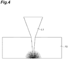
- FIGS. 3 and 4 are views of irradiation states of measurement light and stimulus light in the DUT 10 viewed in a direction perpendicular to optical axes of the measurement light and the stimulus light.
- stimulus light which includes a wavelength associated with an energy higher than a band-gap energy
- intensity modulation is subjected to intensity modulation and the stimulus light is irradiated the DUT 10 with.
- irradiation is performed with measurement light having a different wavelength at a uniform intensity.
- carriers are generated inside the DUT 10 due to the stimulus light, and these carriers become extinct due to recombination at a speed depending on the concentration of impurities and the concentration of defects inside the DUT 10 at a timing when the intensity of the stimulus light is weakened.
- a refraction index and a transmission factor inside the DUT 10 are influenced by the carrier density inside the substrate of the DUT 10. Due to this influence, the measurement light is modulated depending on the modulation state of the stimulus light when the measurement light is reflected on the front surface of the substrate or the rear surface of the substrate.
- the state of modulation of measurement light varies in accordance with the recombination speed of carriers. That is, recombination occurs at a high speed in a region in which the concentration inside the substrate is high, and recombination occurs at a low speed in a region in which the concentration is low.
- the amplitude increases when recombination occurs at a high speed.
- the amplitude decreases when recombination occurs at a low speed and the phase is delayed with respect to stimulus light at the same time.
- FIG. 3 shows a state in which the front surface of the substrate of the DUT 10 on the light irradiation/light guiding system 5 side is set to be irradiated with synthetic light L1 of measurement light and stimulus light.
- the stimulus light generates plenty of electron-positive hole pairs in the vicinity of the front surface of the substrate.
- the DUT 10 is a semiconductor substrate, the DUT 10 has a concentration of impurities to a certain degree.
- a majority of carriers (electrons in a case of an n-type substrate and positive holes in a case of a p-type substrate) are present in a uniform quantity in accordance with this concentration of impurities, and a minority carriers (positive holes in a case of an n-type substrate and electrons in a case of a p-type substrate) are also present.
- the refraction index of the substrate changes due to the carriers, which are present excessively in the incidence region.
- the reflection factor R also changes as the refraction index n changes due to generation and extinction of carriers, and thus reflected light is modulated.
- FIG. 4 shows a state in which the rear surface of the substrate of the DUT 10 on a side opposite to the light irradiation/light guiding system 5 is set to be irradiated with the synthetic light L1 of measurement light and stimulus light in a manner of being transmitted therethrough.
- reflected light also receives the influence of carriers in an optical path in addition to the influence of carriers on the reflection surface in the case of the FIG. 3 .
- an effect of attenuation of light occurs in addition to a change in refraction index due to the carriers in the optical path, and therefore the reflected light is influenced by both.
- An excessively minority carriers become extinct at a speed proportional to the product of the density of a majority carriers, that is, the concentration of impurities in the substrate and the density of an excessively minority carriers (more strictly speaking, an excessively minority carriers is reduced at a speed proportional to the difference with respect to the product of the excess part and a majority carriers).
- the refraction index returns to the original state at a speed proportional to the concentration of impurities in the substrate.
- this change in refraction index is considerably smaller than the extent of the refraction index of the substrate itself.
- the intensity of the reflected light changes substantially in association with a change in refraction index, and a time constant of a change in reflected light with respect to a change in stimulus light is inversely proportional to the concentration of impurities in the substrate.
- the part (a) shows a waveform of a change in stimulus light used for irradiation of the carrier lifetime measurement device 1 over time
- the parts (b) to (d) show waveforms of changes in detection signal detected by the carrier lifetime measurement device 1 over time with respect to stimulus light having the waveform shown in the part (a).
- phase delay appears in a change in amplitude of the detection signal as shown in the part (c).
- a phase delay appears most notably in a change in amplitude of the detection signal when the time constant of a change in reflected light is approximately 1/4 (when the phase delay is 45 degrees) of the repetition cycle T 0 of the stimulus light as shown in the part (d).
- a lifetime from generation to extinction of carriers generated due to incident stimulus light is measured by detecting a phase delay of reflected light with respect to stimulus light in frequencies associated with the concentration of impurities in the measurement target region inside the DUT 10.
- rectangular waves also include not only a component of the repetition frequency but also a frequency component having higher harmonic waves thereof, the lifetime of carriers can be measured efficiently.
- a lifetime of carriers can be measured by repetitively changing the repetition frequency and detecting the detection signal.
- a measurement target region including a defective part is identified using a default defect analyzing method (an analyzing method such as light emission analysis, heat generation analysis, or OBIRCH analysis) in advance, and the measurement target region is set in the controller 37 as a scanning target for the movement control unit 43 and the scanning control unit 45 (identifying step).
- a default defect analyzing method an analyzing method such as light emission analysis, heat generation analysis, or OBIRCH analysis
- the DUT 10 is placed on the stage 3.
- the DUT 10 is a semiconductor device in which a circuit element is formed
- the DUT 10 is placed so that it can be irradiated with measurement light and stimulus light from the rear surface side of the substrate.
- the rear surface may be polished as necessary, and a solid immersion lens may be used.
- the DUT 10 is irradiated with measurement light and stimulus light from the light irradiation/light guiding system 5 (irradiation step).
- the optical axes and the focal depths of the measurement light and the stimulus light are set in advance so that they become the same, and the light irradiation/light guiding system 5 is configured to be an optical system having a sufficiently small chromatic aberration.
- the rear surface of the DUT 10 is subjected to angular adjustment to be perpendicular to the optical axes of the measurement light and the stimulus light, and the focal points of the measurement light and the stimulus light are also set to be focused on a measurement surface of the DUT 10.
- control is performed so that stimulus light is subjected to intensity modulation due to rectangular waves.
- the repetition frequency of these rectangular waves is set in advance in accordance with a postulated concentration of impurities.
- the frequency is set to approximately 1 MHz if the measurement target region is a well part around a transistor, and the frequency is set to several tens of MHz if the measurement target region is a source region or a drain region of a transistor.
- the repetition frequency is set in proportional to the postulated concentration with respect to the concentrations of impurities having other values.
- reflected light from the measurement surface of the DUT 10 is detected, a detection signal is generated, and the detection signal is amplified by the amplifier 31 (outputting step). Further, the component of the repetition frequency and the component of the higher harmonic waves thereof are extracted from the detection signal by the network analyzer 35 of the control system 7. At this time, a band width is set to avoid ground noise of 0 Hz.
- a phase delay with respect to the modulation signal of stimulus light is detected targeting the waveforms of the extracted detection signals having a plurality of frequencies (generation step).
- association data in which information of each of the frequencies of the extracted detection signals and information of a detected phase delay targeting the detection signal are associated with each other is output to the controller 37 from the network analyzer 35 (generation step).
- Detection of the phase delay of the detection signals having the foregoing plurality of frequencies and outputting of association data related thereto may be performed repetitively targeting the plurality of repetition frequencies which have been repetitively set. Consequently, the lifetime of carriers can be measured even when the concentration of impurities or the like is uncertain.
- detection of the phase delay of the detection signals having the foregoing plurality of frequencies and outputting the association data related thereto are performed repetitively while measurement points on the DUT 10 are scanned within the measurement target region due to control of the controller 37.
- the lifetimes of carriers at a plurality of measurement points are computed by the controller 37 using the association data related to the plurality of measurement points within the measurement target region on the DUT 10 (generation step, carrier lifetime computation processing). That is, a frequency at which the phase delay is close to a predetermined value (for example, 45 degrees) is extracted on the basis of the association data, and a combination of the frequency and the phase delay is identified. Accordingly, the phase delays detected in the frequencies associated with the concentrations of impurities at the measurement points are identified. For example, this predetermined value is set to 45 degrees, at which the phase delay is most likely to appear in a change in amplitude of the detection signal, but is not limited thereto.
- a predetermined value for example, 45 degrees
- the lifetimes of carriers at the measurement points on the DUT 10 are computed on the basis of the frequency and the phase delay. At this time, when a frequency having a phase delay close to a predetermined phase delay cannot be extracted, processing of detecting reflected light may be performed repetitively by further changing the repetition frequency.
- the lifetime of carriers is computed as follows.
- a frequency at which the phase delay becomes 45 degrees is referred to as a cutoff frequency, and a time constant ⁇ at this time becomes 1/(2 ⁇ ) times of a cycle associated with this frequency.
- This time constant ⁇ corresponds to a lifetime of carriers inside the DUT 10.
- values of the lifetimes of carriers computed regarding a plurality of measurement points are mapped on an image by the controller 37, data of an output image indicating the distribution of lifetimes of carriers on the DUT 10 is generated (generation step). Further, the output image is output to the input/output device on the basis of the data. With this output image, a fine distribution of lifetimes of carriers on the DUT 10 can be observed within a high-dynamic range in a non-contact manner. For example, unevenness of the lifetime of carriers can be easily observed. As a result, an abnormal place in a circuit element such as a transistor on the DUT 10 can be easily identified.
- the part (a) of FIG. 6 shows a pattern image in which an image of an external appearance of a measurement target region of the DUT 10 is captured, and the part (b) of FIG. 6 shows an output image of a distribution of lifetimes of carriers output by the carrier lifetime measurement device 1 targeting the measurement target region shown in the part (a). In this manner, in an output image, a distribution of lifetimes of carriers is expressed by the gradation of pixels.
- the DUT 10 is irradiated with measurement light and stimulus light subjected to intensity modulation due to a plurality of frequencies, and the intensity of reflected light from the DUT 10 or transmitted light through the DUT 10 is detected.
- image data indicating a distribution of lifetimes of carriers is generated on the basis of an output detection signal.
- a phase delay of a detection signal with respect to a modulation signal including a frequency in association with a concentration of impurities in a measurement target region of the DUT 10 is detected, and a distribution of lifetimes of carriers is measured on the basis of the phase delay. In this manner, even when the concentration of impurities in the measurement target region changes in a variety of ways, it is possible to accurately measure the distribution of lifetimes of carriers.
- irradiation is performed with stimulus light having an energy higher than a band-gap energy of a semiconductor configuring the DUT 10. In this manner, carriers can be generated efficiently in the DUT 10 due to irradiation with stimulus light, and a distribution of lifetimes of carriers can be measured more accurately.
- irradiation is performed with stimulus light subjected to intensity modulation using rectangular waves.
- the frequency of intensity modulation of stimulus light for measuring a phase delay can be set efficiently.
- a region including a defective part in a measurement target object is identified in advance, and measurement is performed targeting the region. In this manner, it is possible to narrow a defective part in advance and to efficiently measure the distribution of lifetimes of carriers at the place. As a result, a defective part in the DUT 10 is easily analyzed.
- irradiation is performed repetitively with stimulus light subjected to intensity modulation for each of a plurality of default frequencies, and in the outputting step, a detection signal is output in association with each ray of the stimulus light.
- a detection signal is output in association with each ray of the stimulus light.
- a phase delay detected in the frequency in association with the concentration of impurities at the measurement points is identified by extracting a frequency at which the phase delay is close to a predetermined value on the basis of association data obtained by measuring reflected light at a plurality of modulation frequencies, but the configuration is not limited to such a method.
- a phase delay detected in the frequency in association with the concentration of impurities indicated by the information may be extracted from the association data on the basis of information of the concentration of impurities related to the measurement target region input to the controller 37 in advance via the input/output device or the like.
- the controller 37 may perform control so that a phase delay is detected and output in only the frequency in association with the concentration of impurities by controlling the network analyzer 35.
- the lifetime of carriers may be computed on the basis of the frequency in association with the concentration of impurities and the extracted phase delay.
- the light irradiation/light guiding system 5 of the foregoing embodiment is configured to be able to guide reflected light from the DUT 10 toward the control system 7 but may be configured to be able to guide transmitted light generated when measurement light is transmitted through the DUT 10 toward the control system 7. In this case, a lifetime of carriers is measured on the basis of the detection signal generated by detecting transmitted light in the control system 7.
- the light irradiation/light guiding system 5 of the foregoing embodiment may include a fiber coupler as an element for synthesizing measurement light and stimulus light in place of the dichroic mirror 13 or may include fibers having a plurality of cores.
- the polarization beam splitter 15 may be disposed between the dichroic mirror 13 and the light source 9a.
- the dichroic mirror 13 plays a role of the optical filter 25.
- the light irradiation/light guiding system 5 of the foregoing embodiment is configured so that the optical axes and the focal points coincide with each other between measurement light and stimulus light.
- the optical axes and the focal points coincide with each other between measurement light and stimulus light.
- the optical axes may be set in a misaligned manner between measurement light and stimulus light.
- the optical filter 25 may be omitted.
- measurement is performed using stimulus light subjected to intensity modulation due to rectangular waves.
- a plurality of rays of stimulus light which are subjected to intensity modulation using a signal having a different waveform such as sine waves and which are associated with a plurality of respective frequencies may be used.
- the modulation unit perform intensity modulation of stimulus light using rectangular waves. In this case, it is possible to efficiently set a frequency of intensity modulation of stimulus light for measuring a phase delay. As a result, even when the concentration of impurities changes in a variety of ways, it is possible to efficiently measure the distribution of lifetimes of carriers.
- the irradiation step that irradiation be performed with stimulus light subjected to intensity modulation for each of a plurality of default frequencies and in the outputting step, a detection signal be output in association with each ray of the stimulus light.
- the second light source generate stimulus light subjected to intensity modulation by the modulation unit for each of a plurality of default frequencies and the photo detector output a detection signal in association with each ray of the stimulus light.
- the foregoing embodiment further include an identifying step of identifying a region including a defective part in a measurement target object in advance so that the region is irradiated with reflected light and stimulus light in the irradiation step and a detection signal is output targeting the region in the outputting step.
- an identifying step of identifying a region including a defective part in a measurement target object in advance so that the region is irradiated with reflected light and stimulus light in the irradiation step and a detection signal is output targeting the region in the outputting step.
- a phase delay with respect to a modulation signal including a frequency associated with information of a concentration of impurities input in advance be detected.
- the analysis unit detect a phase delay with respect to a modulation signal including a frequency associated with information of a concentration of impurities input in advance.
- the irradiation step it is favorable, in the irradiation step, that irradiation be performed with stimulus light having an energy higher than a band-gap energy of a measurement target object.
- the second light source it is favorable that the second light source generate stimulus light having an energy higher than a band-gap energy of a measurement target object. In this case, carriers can be generated efficiently in a measurement target object due to irradiation with stimulus light, and a distribution of lifetimes of carriers can be measured more accurately.
- An embodiment is used for a carrier lifetime measurement method and a carrier lifetime measurement device for measuring a lifetime of carriers in a measurement target object, and it is possible to accurately measure a lifetime of carriers in a measurement target object.
Landscapes
- Physics & Mathematics (AREA)
- General Physics & Mathematics (AREA)
- General Health & Medical Sciences (AREA)
- Chemical & Material Sciences (AREA)
- Analytical Chemistry (AREA)
- Biochemistry (AREA)
- Life Sciences & Earth Sciences (AREA)
- Health & Medical Sciences (AREA)
- Immunology (AREA)
- Pathology (AREA)
- Investigating Or Analysing Materials By Optical Means (AREA)
- Testing Or Measuring Of Semiconductors Or The Like (AREA)
- Investigating Or Analyzing Materials By The Use Of Electric Means (AREA)
Abstract
Description
- The present disclosure relates to a carrier lifetime measurement method and a carrier lifetime measurement device for measuring a lifetime of carriers in a measurement target object.
- In the related art, a device for performing characteristic evaluation of a measurement target object such as a solar battery is known (for example, refer to the following Patent Literature 1). This device is configured to have a pumping light source irradiating a measurement target object with pulsed pumping light, a probe light source continuously irradiating the measurement target object with probe light, a photo detector detecting the probe light used for irradiating the measurement target object in real time, and a signal processing unit processing a signal output from the photo-detector. According to such a configuration, it is possible to measure circumstances of generation and extinction of carriers by measuring a change in carrier quantity over time.
- [Patent Literature 1] Japanese Unexamined Patent Publication No.
2016-157780 - In such devices in the related art described above, although a change in carrier quantity over time can be measured, it is difficult to measure an exact lifetime of carriers targeting a measurement target object whose concentration of impurities is unknown.
- An embodiment aims to provide a carrier lifetime measurement method and a carrier lifetime measurement device capable of accurately measuring a lifetime of carriers in a measurement target object.
- According to an aspect of the present invention, there is provided a carrier lifetime measurement method for measuring a lifetime of carriers in a measurement target object. The carrier lifetime measurement method includes an irradiation step of irradiating the measurement target object with measurement light and stimulus light subjected to intensity modulation using a plurality of frequencies, an outputting step of outputting a detection signal by detecting an intensity of reflected light from the measurement target object or transmitted light through the measurement target object, and a generation step of detecting a phase delay of the detection signal with respect to a modulation signal including a frequency in association with a concentration of impurities in a measurement target region of the plurality of frequencies and generating image data indicating a distribution of lifetimes of carriers in the measurement target object on the basis of the phase delay.
- Alternatively, according to another aspect of the present invention, there is provided a carrier lifetime measurement device for measuring a lifetime of carriers in a measurement target object. The carrier lifetime measurement device includes a first light source configured to generate measurement light, a second light source configured to generate stimulus light, a modulation unit configured to perform intensity modulation of the stimulus light using a plurality of frequencies, a photo detector configured to output a detection signal by detecting an intensity of reflected light from the measurement target object or transmitted light through the measurement target object, an optical system configured to guide the measurement light and the stimulus light subjected to intensity modulation toward the measurement target object and to guide reflected light from the measurement target object or transmitted light through the measurement target object toward the photo detector, and an analysis unit configured detect a phase delay of the detection signal with respect to a modulation signal including a frequency in association with a concentration of impurities in a measurement target region of the plurality of frequencies, and to generate image data indicating a distribution of lifetimes of carriers in the measurement target object on the basis of the phase delay.
- According to any of the foregoing aspects, a measurement target object is irradiated with measurement light and stimulus light subjected to intensity modulation using a plurality of frequencies, and an intensity of reflected light from the measurement target object or transmitted light through the measurement target object is detected. As a result, image data indicating a distribution of lifetimes of carriers is generated on the basis of an output detection signal. At this time, a phase delay of a detection signal with respect to a modulation signal including a frequency in association with a concentration of impurities in a measurement target region is detected, and a distribution of lifetimes of carriers is measured on the basis of the phase delay. In this manner, even when a concentration of impurities in a measurement target region changes in a variety of ways, it is possible to accurately measure a distribution of lifetimes of carriers.
- According to an embodiment, it is possible to accurately measure a lifetime of carriers in a measurement target object.
-
-
FIG. 1 is a view of a schematic configuration of a carrier lifetime measurement device 1 according to an embodiment. -
FIG. 2 is a block diagram showing a configuration of functions of acontroller 37 inFIG. 1 . -
FIG. 3 is a view of an irradiation state of measurement light and stimulus light in aDUT 10 viewed in a direction perpendicular to optical axes of the measurement light and the stimulus light. -
FIG. 4 is a view of another irradiation state of measurement light and stimulus light in theDUT 10 viewed in a direction perpendicular to the optical axes of the measurement light and the stimulus light. -
FIG. 5 is a view showing waveforms of changes in stimulus light and detection signal over time generated by the carrier lifetime measurement device 1. -
FIG. 6(a) is a view showing a pattern image in which an image of an external appearance of a measurement target region of theDUT 10 is captured, andFIG. 6(b) is a view showing an output image of a distribution of lifetimes of carriers output by the carrier lifetime measurement device 1 targeting the measurement target region shown inFIG. 6(a) . - Hereinafter, an embodiment of the present invention will be described in detail with reference to the accompanying drawings. In the description, the same reference signs are applied to the same elements or elements having the same function, and duplicate description will be omitted.
-
FIG. 1 is a view of a schematic configuration of a carrier lifetime measurement device 1 according to the embodiment. The carrier lifetime measurement device 1 shown inFIG. 1 is a device for measuring a lifetime of carriers in a device under test (DUT) 10 serving as a measurement target object such as a semiconductor device by performing optical measurement targeting theDUT 10. Regarding a measurement target of the carrier lifetime measurement device 1, a semiconductor device in which a circuit element such as a transistor is formed on a semiconductor substrate is favorably used. More favorably, a region which is estimated to include a defective part using a default defect analyzing method (an analyzing method such as light emission analysis, heat generation analysis, or optical beam induced resistance change (OBIRCH) analysis) in advance may be adopted as a measurement target. - This carrier lifetime measurement device 1 is configured to include a
stage 3 on which theDUT 10 is disposed; a light irradiation/light guiding system (optical system) 5 which guides light toward theDUT 10, irradiates theDUT 10 with the light, and guides reflected light from theDUT 10; and acontrol system 7 which controls the light irradiation/light guidingsystem 5, detects reflected light from theDUT 10, and performs processing of the reflected light. Thestage 3 is a support unit supporting theDUT 10 so that theDUT 10 faces the light irradiation/light guidingsystem 5. Thestage 3 may be equipped with a movement mechanism which can move theDUT 10 relatively to the light irradiation/light guidingsystem 5. InFIG. 1 , a traveling path of light is indicated by a dashed-dotted line, and a transmission path of a control signal and transmission paths of a detection signal and processing data are indicated by solid arrows. - The light irradiation/light guiding
system 5 includes a light source (first light source) 9a, a light source (second light source) 9b,collimators dichroic mirror 13, apolarization beam splitter 15, a quarter-wavelength plate 17, agalvanometer mirror 19, apupil projection lens 21, anobject lens 23, anoptical filter 25, and acollimator 27. - The
light source 9a generates and emits light as measurement light (probe light) that has a wavelength and an intensity suitable for detecting optical characteristics which change in association with the concentration of impurities in theDUT 10. Thelight source 9b generates and emits light as stimulus light (pumping light) that includes a wavelength component which is partially absorbed in theDUT 10. Specifically, thelight source 9b is set to generate stimulus light including a wavelength associated with an energy higher than a band-gap energy of a semiconductor which is a material for a substrate configuring theDUT 10. Moreover, thislight source 9b is configured to be able to generate stimulus light subjected to intensity modulation on the basis of an electrical signal from the outside. For example, thelight source 9a and thelight source 9b may be coherent light sources such as semiconductor lasers or may be incoherent light sources such as super luminescent diodes (SLDs). - The
collimators light sources dichroic mirror 13 coaxially synthesizes measurement light and stimulus light which have been collimated and outputs the coaxially synthesized light toward thepolarization beam splitter 15. Thepolarization beam splitter 15 allows linearly polarized components of measurement light and stimulus light which have been synthesized to be transmitted therethrough, and the quarter-wavelength plate 17 changes polarization states of the measurement light and the stimulus light which have been transmitted through thepolarization beam splitter 15 and sets the polarization states of the measurement light and the stimulus light in circular polarization. Thegalvanometer mirror 19 performs scanning with measurement light and stimulus light in circular polarization and outputs the measurement light and the stimulus light, and thepupil projection lens 21 relays pupils of measurement light and stimulus light output from thegalvanometer mirror 19 to a pupil of theobject lens 23 from thegalvanometer mirror 19. Theobject lens 23 collects measurement light and stimulus light on theDUT 10. According to such a configuration, a desired position on theDUT 10 can be scanned and irradiated with measurement light and stimulus light which have been synthesized. In addition, the carrier lifetime measurement device 1 may be configured to be able to perform scanning with measurement light and stimulus light targeting a range which thegalvanometer mirror 19 cannot cover by moving thestage 3. - In addition, in the light irradiation/light guiding
system 5 having the foregoing configuration, reflected light from theDUT 10 can be guided to the quarter-wavelength plate 17 in a manner of being coaxial with measurement light and stimulus light, and the polarization state of reflected light can be changed from circular polarization to linear polarization by the quarter-wavelength plate 17. Moreover, linearly polarized reflected light is reflected toward theoptical filter 25 and thecollimator 27 by thepolarization beam splitter 15. Theoptical filter 25 is configured to allow only the same wavelength component as that of measurement light of reflected light to be transmitted therethrough toward thecollimator 27 and to block the same wavelength component as that of stimulus light of reflected light. Thecollimator 27 collimates reflected light and outputs the reflected light toward thecontrol system 7 via an optical fiber or the like. - The
control system 7 includes aphoto detector 29, anamplifier 31, a modulation signal source (modulation unit) 33, a network analyzer 35 (analysis unit), a controller (analysis unit) 37, and alaser scanning controller 39. - The
photo detector 29 is a photo detection element such as a photodiode (PD), an avalanche photodiode (APD), or a photomultiplier tube, which receives reflected light guided by the light irradiation/light guidingsystem 5, detects the intensity of the reflected light, and outputs a detection signal. Theamplifier 31 amplifies a detection signal output from thephoto detector 29 and outputs an amplified result to thenetwork analyzer 35. Themodulation signal source 33 generates an electrical signal (modulation signal) having a waveform set by thecontroller 37 and controls thelight source 9b so that stimulus light is subjected to intensity modulation on the basis of the electrical signal. Specifically, themodulation signal source 33 generates an electrical signal having rectangular waves of a set repetition frequency (default frequency) and controls thelight source 9b on the basis of the electrical signal. In addition, themodulation signal source 33 also has a function of repetitively generating an electrical signal having rectangular waves of a plurality of repetition frequencies. Stimulus light subjected to intensity modulation due to each of rectangular waves of repetition frequencies includes components of a plurality of frequencies including the repetition frequencies and frequencies having higher harmonic waves thereof. - The network analyzer 35 extracts and detects a detection signal having a wavelength component associated with the repetition frequency on the basis of a detection signal output from the
amplifier 31 and the repetition frequency set by themodulation signal source 33. Specifically, thenetwork analyzer 35 extracts a detection signal having the same frequency as the repetition frequency and a detection signal having a frequency of higher harmonic waves thereof. Moreover, thenetwork analyzer 35 detects a phase delay of a detection signal having each of the frequencies with respect to stimulus light subjected to intensity modulation on the basis of an electrical signal generated by themodulation signal source 33. Further, thenetwork analyzer 35 inputs information of each of the frequencies of the extracted detection signals and information of a detected phase delay targeting the detection signal to thecontroller 37 in an associated manner. At this time, thenetwork analyzer 35 may repetitively extract a detection signal targeting an electrical signal having a plurality of repetition frequencies which have been repetitively set by thecontroller 37 and may detect a phase delay targeting the detection signal. For example, a phase delay may be detected by changing the repetition frequency from a fundamental frequency to frequencies of 1/10 times, ten times, and the like. Here, thenetwork analyzer 35 may be changed to a spectrum analyzer, may be changed to a lock-in amplifier, or may be changed to a configuration in which a digitizer and an FFT analyzer are combined. - The
controller 37 is a device for generally controlling operation of thecontrol system 7 and is physically a control device such as a computer including a central processing unit (CPU) serving as a processor, a random access memory (RAM) and a read only memory (ROM) serving as recording mediums, a communication module, and input/output devices such as a display, a mouse, a keyboard, and the like.FIG. 2 shows a configuration of functions of thecontroller 37. As shown inFIG. 2 , as functional constituent elements, thecontroller 37 is configured to include amodulation control unit 41, amovement control unit 43, ascanning control unit 45, a carrierlifetime computation unit 47, and anoutput unit 49. - The
modulation control unit 41 of thecontroller 37 sets a waveform of an electrical signal for performing intensity modulation of stimulus light. Specifically, themodulation control unit 41 sets a waveform of an electrical signal to have rectangular waves of a predetermined repetition frequency. This "predetermined repetition frequency" may be a frequency having a value stored in thecontroller 37 in advance in accordance with a concentration of impurities or the like in a postulatedDUT 10 or may be a frequency having a value input from the outside via the input/output device. In addition, themodulation control unit 41 may repetitively change the repetition frequency from a fundamental frequency which has been recorded or input in advance to a plurality of frequencies and may be able to set an electrical signal in accordance with the changed repetition frequencies. - The
movement control unit 43 and thescanning control unit 45 respectively control thestage 3 and thegalvanometer mirror 19 to perform scanning with measurement light and stimulus light on theDUT 10. At this time, themovement control unit 43 performs control so that scanning is performed with measurement light and stimulus light while carrier lifetime computation processing (which will be described below) is performed targeting each of the places in theDUT 10. - The carrier
lifetime computation unit 47 computes a lifetime of carriers targeting each of the places in a measurement target region of theDUT 10 on the basis of information of the phase delay for each of the frequencies of the detection signals output from thenetwork analyzer 35 and executes carrier lifetime computation processing (details of carrier lifetime computation processing will be described below) for generating image data indicating a distribution of lifetimes of carriers within the measurement target region. Theoutput unit 49 outputs image data generated by the carrierlifetime computation unit 47 to the input/output device as an image. - A phenomenon measured by the carrier lifetime measurement device 1 having the foregoing configuration will be described.
FIGS. 3 and4 are views of irradiation states of measurement light and stimulus light in theDUT 10 viewed in a direction perpendicular to optical axes of the measurement light and the stimulus light. - Due to the light irradiation/
light guiding system 5, stimulus light, which includes a wavelength associated with an energy higher than a band-gap energy, is subjected to intensity modulation and the stimulus light is irradiated theDUT 10 with. At the same time, irradiation is performed with measurement light having a different wavelength at a uniform intensity. At this time, carriers are generated inside theDUT 10 due to the stimulus light, and these carriers become extinct due to recombination at a speed depending on the concentration of impurities and the concentration of defects inside theDUT 10 at a timing when the intensity of the stimulus light is weakened. - A refraction index and a transmission factor inside the
DUT 10 are influenced by the carrier density inside the substrate of theDUT 10. Due to this influence, the measurement light is modulated depending on the modulation state of the stimulus light when the measurement light is reflected on the front surface of the substrate or the rear surface of the substrate. The state of modulation of measurement light varies in accordance with the recombination speed of carriers. That is, recombination occurs at a high speed in a region in which the concentration inside the substrate is high, and recombination occurs at a low speed in a region in which the concentration is low. As a result, regarding reflected light generated due to reflection of measurement light, the amplitude increases when recombination occurs at a high speed. On the other hand, the amplitude decreases when recombination occurs at a low speed and the phase is delayed with respect to stimulus light at the same time. -
FIG. 3 shows a state in which the front surface of the substrate of theDUT 10 on the light irradiation/light guiding system 5 side is set to be irradiated with synthetic light L1 of measurement light and stimulus light. In this case, the stimulus light generates plenty of electron-positive hole pairs in the vicinity of the front surface of the substrate. When theDUT 10 is a semiconductor substrate, theDUT 10 has a concentration of impurities to a certain degree. Therefore, a majority of carriers (electrons in a case of an n-type substrate and positive holes in a case of a p-type substrate) are present in a uniform quantity in accordance with this concentration of impurities, and a minority carriers (positive holes in a case of an n-type substrate and electrons in a case of a p-type substrate) are also present. When stimulus light is incident in this state, the refraction index of the substrate changes due to the carriers, which are present excessively in the incidence region. It is known that a reflection factor R between atmospheric air and a substrate is expressed by the following expression R=((n-1)/(n+1))2 when the refraction index of atmospheric air is "1" and the refraction index of the substrate is n. The reflection factor R also changes as the refraction index n changes due to generation and extinction of carriers, and thus reflected light is modulated. - Meanwhile,
FIG. 4 shows a state in which the rear surface of the substrate of theDUT 10 on a side opposite to the light irradiation/light guiding system 5 is set to be irradiated with the synthetic light L1 of measurement light and stimulus light in a manner of being transmitted therethrough. In this case, reflected light also receives the influence of carriers in an optical path in addition to the influence of carriers on the reflection surface in the case of theFIG. 3 . Specifically, an effect of attenuation of light occurs in addition to a change in refraction index due to the carriers in the optical path, and therefore the reflected light is influenced by both. An excessively minority carriers become extinct at a speed proportional to the product of the density of a majority carriers, that is, the concentration of impurities in the substrate and the density of an excessively minority carriers (more strictly speaking, an excessively minority carriers is reduced at a speed proportional to the difference with respect to the product of the excess part and a majority carriers). As a result, when stimulus light decreases, the refraction index returns to the original state at a speed proportional to the concentration of impurities in the substrate. However, this change in refraction index is considerably smaller than the extent of the refraction index of the substrate itself. - When the reflected light in the case shown in
FIG. 3 or4 is observed, the intensity of the reflected light changes substantially in association with a change in refraction index, and a time constant of a change in reflected light with respect to a change in stimulus light is inversely proportional to the concentration of impurities in the substrate. - In
FIG. 5 , the part (a) shows a waveform of a change in stimulus light used for irradiation of the carrier lifetime measurement device 1 over time, and the parts (b) to (d) show waveforms of changes in detection signal detected by the carrier lifetime measurement device 1 over time with respect to stimulus light having the waveform shown in the part (a). When a repetition cycle T0 of the stimulus light is considerably larger than the time constant of a change in reflected light (the repetition frequency is low), the sensitivity of the phase delay observed in the detection signal becomes low as shown in the part (b). When the time constant of a change in reflected light is approximately half the repetition cycle T0 of the stimulus light (when the time constant is comparatively large and the phase delay is approximately 90 degrees), a phase delay appears in a change in amplitude of the detection signal as shown in the part (c). A phase delay appears most notably in a change in amplitude of the detection signal when the time constant of a change in reflected light is approximately 1/4 (when the phase delay is 45 degrees) of the repetition cycle T0 of the stimulus light as shown in the part (d). - In the present embodiment, a lifetime from generation to extinction of carriers generated due to incident stimulus light is measured by detecting a phase delay of reflected light with respect to stimulus light in frequencies associated with the concentration of impurities in the measurement target region inside the
DUT 10. Here, since rectangular waves also include not only a component of the repetition frequency but also a frequency component having higher harmonic waves thereof, the lifetime of carriers can be measured efficiently. Moreover, even when the concentration inside theDUT 10 is uncertain, a lifetime of carriers can be measured by repetitively changing the repetition frequency and detecting the detection signal. - Hereinafter, details of a measurement procedure including the carrier lifetime computation processing in the carrier lifetime measurement device 1 will be described.
- First, in a case of the
DUT 10 being a semiconductor device in which abnormal operation is caused, a measurement target region including a defective part is identified using a default defect analyzing method (an analyzing method such as light emission analysis, heat generation analysis, or OBIRCH analysis) in advance, and the measurement target region is set in thecontroller 37 as a scanning target for themovement control unit 43 and the scanning control unit 45 (identifying step). - Next, the
DUT 10 is placed on thestage 3. For example, when theDUT 10 is a semiconductor device in which a circuit element is formed, theDUT 10 is placed so that it can be irradiated with measurement light and stimulus light from the rear surface side of the substrate. When theDUT 10 is irradiated from the rear surface side, the rear surface may be polished as necessary, and a solid immersion lens may be used. - Thereafter, the
DUT 10 is irradiated with measurement light and stimulus light from the light irradiation/light guiding system 5 (irradiation step). At this time, the optical axes and the focal depths of the measurement light and the stimulus light are set in advance so that they become the same, and the light irradiation/light guiding system 5 is configured to be an optical system having a sufficiently small chromatic aberration. At this time, the rear surface of theDUT 10 is subjected to angular adjustment to be perpendicular to the optical axes of the measurement light and the stimulus light, and the focal points of the measurement light and the stimulus light are also set to be focused on a measurement surface of theDUT 10. - Moreover, due to control of the
controller 37, control is performed so that stimulus light is subjected to intensity modulation due to rectangular waves. The repetition frequency of these rectangular waves is set in advance in accordance with a postulated concentration of impurities. For example, the frequency is set to approximately 1 MHz if the measurement target region is a well part around a transistor, and the frequency is set to several tens of MHz if the measurement target region is a source region or a drain region of a transistor. The repetition frequency is set in proportional to the postulated concentration with respect to the concentrations of impurities having other values. - Next, in the
photo detector 29 of thecontrol system 7, reflected light from the measurement surface of theDUT 10 is detected, a detection signal is generated, and the detection signal is amplified by the amplifier 31 (outputting step). Further, the component of the repetition frequency and the component of the higher harmonic waves thereof are extracted from the detection signal by thenetwork analyzer 35 of thecontrol system 7. At this time, a band width is set to avoid ground noise of 0 Hz. - In addition, in the
network analyzer 35 of thecontrol system 7, a phase delay with respect to the modulation signal of stimulus light is detected targeting the waveforms of the extracted detection signals having a plurality of frequencies (generation step). Moreover, association data in which information of each of the frequencies of the extracted detection signals and information of a detected phase delay targeting the detection signal are associated with each other is output to thecontroller 37 from the network analyzer 35 (generation step). - Detection of the phase delay of the detection signals having the foregoing plurality of frequencies and outputting of association data related thereto may be performed repetitively targeting the plurality of repetition frequencies which have been repetitively set. Consequently, the lifetime of carriers can be measured even when the concentration of impurities or the like is uncertain. In addition, detection of the phase delay of the detection signals having the foregoing plurality of frequencies and outputting the association data related thereto are performed repetitively while measurement points on the
DUT 10 are scanned within the measurement target region due to control of thecontroller 37. - Thereafter, the lifetimes of carriers at a plurality of measurement points are computed by the
controller 37 using the association data related to the plurality of measurement points within the measurement target region on the DUT 10 (generation step, carrier lifetime computation processing). That is, a frequency at which the phase delay is close to a predetermined value (for example, 45 degrees) is extracted on the basis of the association data, and a combination of the frequency and the phase delay is identified. Accordingly, the phase delays detected in the frequencies associated with the concentrations of impurities at the measurement points are identified. For example, this predetermined value is set to 45 degrees, at which the phase delay is most likely to appear in a change in amplitude of the detection signal, but is not limited thereto. Further, the lifetimes of carriers at the measurement points on theDUT 10 are computed on the basis of the frequency and the phase delay. At this time, when a frequency having a phase delay close to a predetermined phase delay cannot be extracted, processing of detecting reflected light may be performed repetitively by further changing the repetition frequency. - More specifically, the lifetime of carriers is computed as follows. A frequency at which the phase delay becomes 45 degrees is referred to as a cutoff frequency, and a time constant τ at this time becomes 1/(2π) times of a cycle associated with this frequency. This time constant τ corresponds to a lifetime of carriers inside the
DUT 10. Utilizing this property, a lifetime LT of carriers is computed using the following expression LT=tanΔθ/(2πF) on the basis of a frequency F and a phase delay Δθ extracted from association data. - Lastly, values of the lifetimes of carriers computed regarding a plurality of measurement points are mapped on an image by the
controller 37, data of an output image indicating the distribution of lifetimes of carriers on theDUT 10 is generated (generation step). Further, the output image is output to the input/output device on the basis of the data. With this output image, a fine distribution of lifetimes of carriers on theDUT 10 can be observed within a high-dynamic range in a non-contact manner. For example, unevenness of the lifetime of carriers can be easily observed. As a result, an abnormal place in a circuit element such as a transistor on theDUT 10 can be easily identified. - The part (a) of
FIG. 6 shows a pattern image in which an image of an external appearance of a measurement target region of theDUT 10 is captured, and the part (b) ofFIG. 6 shows an output image of a distribution of lifetimes of carriers output by the carrier lifetime measurement device 1 targeting the measurement target region shown in the part (a). In this manner, in an output image, a distribution of lifetimes of carriers is expressed by the gradation of pixels. - According to the carrier lifetime measurement device 1 described above and a carrier lifetime measurement method using the carrier lifetime measurement device 1, the
DUT 10 is irradiated with measurement light and stimulus light subjected to intensity modulation due to a plurality of frequencies, and the intensity of reflected light from theDUT 10 or transmitted light through theDUT 10 is detected. As a result, image data indicating a distribution of lifetimes of carriers is generated on the basis of an output detection signal. At this time, a phase delay of a detection signal with respect to a modulation signal including a frequency in association with a concentration of impurities in a measurement target region of theDUT 10 is detected, and a distribution of lifetimes of carriers is measured on the basis of the phase delay. In this manner, even when the concentration of impurities in the measurement target region changes in a variety of ways, it is possible to accurately measure the distribution of lifetimes of carriers. - In addition, in the irradiation step of the carrier lifetime measurement method of the present embodiment, irradiation is performed with stimulus light having an energy higher than a band-gap energy of a semiconductor configuring the
DUT 10. In this manner, carriers can be generated efficiently in theDUT 10 due to irradiation with stimulus light, and a distribution of lifetimes of carriers can be measured more accurately. - In addition, in the irradiation step of the carrier lifetime measurement method, irradiation is performed with stimulus light subjected to intensity modulation using rectangular waves. In this case, the frequency of intensity modulation of stimulus light for measuring a phase delay can be set efficiently. As a result, even when the concentration of impurities changes in a variety of ways, it is possible to efficiently measure the distribution of lifetimes of carriers.
- Moreover, in the carrier lifetime measurement method, a region including a defective part in a measurement target object is identified in advance, and measurement is performed targeting the region. In this manner, it is possible to narrow a defective part in advance and to efficiently measure the distribution of lifetimes of carriers at the place. As a result, a defective part in the
DUT 10 is easily analyzed. - In addition, in the irradiation step of the carrier lifetime measurement method, irradiation is performed repetitively with stimulus light subjected to intensity modulation for each of a plurality of default frequencies, and in the outputting step, a detection signal is output in association with each ray of the stimulus light. In this case, even when the concentration of impurities changes extensively, it is possible to set a frequency of stimulus light causing a phase delay associated therewith. As a result, even when the concentration of impurities changes extensively, it is possible to accurately measure a lifetime of carriers.
- Hereinabove, various embodiments of the present invention have been described. However, the present invention is not limited to the foregoing embodiments and may be modified or may be applied to other configurations within a range which does not change the gist described in each of the claims.
- In the generation step of the carrier lifetime measurement method in the foregoing embodiment, a phase delay detected in the frequency in association with the concentration of impurities at the measurement points is identified by extracting a frequency at which the phase delay is close to a predetermined value on the basis of association data obtained by measuring reflected light at a plurality of modulation frequencies, but the configuration is not limited to such a method.
- That is, in the generation step, a phase delay detected in the frequency in association with the concentration of impurities indicated by the information may be extracted from the association data on the basis of information of the concentration of impurities related to the measurement target region input to the
controller 37 in advance via the input/output device or the like. At this time, thecontroller 37 may perform control so that a phase delay is detected and output in only the frequency in association with the concentration of impurities by controlling thenetwork analyzer 35. Further, the lifetime of carriers may be computed on the basis of the frequency in association with the concentration of impurities and the extracted phase delay. - According to such a configuration, it is possible to suitably set a frequency of a phase delay detected so as to compute a lifetime of carriers. As a result, it is possible to efficiently measure the distribution of lifetimes of carriers.
- The light irradiation/
light guiding system 5 of the foregoing embodiment is configured to be able to guide reflected light from theDUT 10 toward thecontrol system 7 but may be configured to be able to guide transmitted light generated when measurement light is transmitted through theDUT 10 toward thecontrol system 7. In this case, a lifetime of carriers is measured on the basis of the detection signal generated by detecting transmitted light in thecontrol system 7. - The light irradiation/
light guiding system 5 of the foregoing embodiment may include a fiber coupler as an element for synthesizing measurement light and stimulus light in place of thedichroic mirror 13 or may include fibers having a plurality of cores. - In the light irradiation/
light guiding system 5 of the foregoing embodiment, thepolarization beam splitter 15 may be disposed between thedichroic mirror 13 and thelight source 9a. In this case, thedichroic mirror 13 plays a role of theoptical filter 25. - The light irradiation/
light guiding system 5 of the foregoing embodiment is configured so that the optical axes and the focal points coincide with each other between measurement light and stimulus light. However, if spots of stimulus light at the measurement points in theDUT 10 include spots of measurement light, the focal points do not necessarily coincide with each other. In addition, when fibers having a plurality of cores are used, the optical axes may be set in a misaligned manner between measurement light and stimulus light. - In addition, in the foregoing embodiment, if the
photo detector 29 is configured to be sensitive to only measurement light, theoptical filter 25 may be omitted. - In addition, in the foregoing embodiment, measurement is performed using stimulus light subjected to intensity modulation due to rectangular waves. However, a plurality of rays of stimulus light which are subjected to intensity modulation using a signal having a different waveform such as sine waves and which are associated with a plurality of respective frequencies may be used.
- In the foregoing embodiment, it is also favorable, in the irradiation step, that irradiation be performed with stimulus light subjected to intensity modulation due to rectangular waves. In addition, it is also favorable that the modulation unit perform intensity modulation of stimulus light using rectangular waves. In this case, it is possible to efficiently set a frequency of intensity modulation of stimulus light for measuring a phase delay. As a result, even when the concentration of impurities changes in a variety of ways, it is possible to efficiently measure the distribution of lifetimes of carriers.
- In addition, it is also favorable, in the irradiation step, that irradiation be performed with stimulus light subjected to intensity modulation for each of a plurality of default frequencies and in the outputting step, a detection signal be output in association with each ray of the stimulus light. In addition, it is also favorable that the second light source generate stimulus light subjected to intensity modulation by the modulation unit for each of a plurality of default frequencies and the photo detector output a detection signal in association with each ray of the stimulus light. In this case, even when the concentration of impurities changes extensively, it is possible to set a frequency of stimulus light causing a phase delay in association therewith. As a result, even when the concentration of impurities changes extensively, it is possible to accurately measure a lifetime of carriers.
- Moreover, it is also favorable that the foregoing embodiment further include an identifying step of identifying a region including a defective part in a measurement target object in advance so that the region is irradiated with reflected light and stimulus light in the irradiation step and a detection signal is output targeting the region in the outputting step. In this manner, it is possible to narrow a defective part in advance and to efficiently measure the distribution of lifetimes of carriers at the place. As a result, a defective part in a measurement target object is easily analyzed.
- Furthermore, it is also favorable, in the generation step, that a phase delay with respect to a modulation signal including a frequency associated with information of a concentration of impurities input in advance be detected. Furthermore, it is also favorable that the analysis unit detect a phase delay with respect to a modulation signal including a frequency associated with information of a concentration of impurities input in advance. When such a configuration is employed, it is possible to simply set a frequency of a phase delay detected for computing a lifetime of carriers. As a result, it is possible to efficiently measure a distribution of lifetimes of carriers.
- In addition, it is favorable, in the irradiation step, that irradiation be performed with stimulus light having an energy higher than a band-gap energy of a measurement target object. In another embodiment described above, it is favorable that the second light source generate stimulus light having an energy higher than a band-gap energy of a measurement target object. In this case, carriers can be generated efficiently in a measurement target object due to irradiation with stimulus light, and a distribution of lifetimes of carriers can be measured more accurately.
- An embodiment is used for a carrier lifetime measurement method and a carrier lifetime measurement device for measuring a lifetime of carriers in a measurement target object, and it is possible to accurately measure a lifetime of carriers in a measurement target object.
-
- 1
- Carrier lifetime measurement device
- 5
- Light irradiation/light guiding system (optical system)
- 7
- Control system
- 9a
- Light source (first light source)
- 9b
- Light source (second light source)
- 29
- Photo-detector
- 33
- Modulation signal source (modulation unit)
- 35
- Network analyzer (analysis unit)
- 37
- Controller (analysis unit)
Claims (12)
- A carrier lifetime measurement method for measuring a lifetime of carriers in a measurement target object, the carrier lifetime measurement method comprising:an irradiation step of irradiating the measurement target object with measurement light and stimulus light subjected to intensity modulation using a plurality of frequencies;an outputting step of outputting a detection signal by detecting an intensity of reflected light from the measurement target object or transmitted light through the measurement target object; anda generation step of detecting a phase delay of the detection signal with respect to a modulation signal including a frequency in association with a concentration of impurities in a measurement target region of the plurality of frequencies and generating image data indicating a distribution of lifetimes of carriers in the measurement target object on the basis of the phase delay.
- The carrier lifetime measurement method according to claim 1,
wherein in the irradiation step, irradiation is performed with the stimulus light subjected to intensity modulation using rectangular waves. - The carrier lifetime measurement method according to claim 1,
wherein in the irradiation step, irradiation is performed with the stimulus light subjected to intensity modulation for each of a plurality of default frequencies, and
wherein in the outputting step, the detection signal associated with each ray of the stimulus light is output. - The carrier lifetime measurement method according to any one of claims 1 to 3, further comprising:an identifying step of identifying a region including a defective part in the measurement target object in advance,wherein in the irradiation step, the region is irradiated with the reflected light and the stimulus light, andwherein in the outputting step, the detection signal is output targeting the region.
- The carrier lifetime measurement method according to any one of claims 1 to 4,
wherein in the generation step, the phase delay with respect to a modulation signal including a frequency associated with information of a concentration of impurities input in advance is detected. - The carrier lifetime measurement method according to any one of claims 1 to 5,
wherein in the irradiation step, irradiation is performed with stimulus light having an energy higher than a band-gap energy of the measurement target object. - The carrier lifetime measurement method according to any one of claims 1 to 6,
wherein the measurement target object is a semiconductor device. - A carrier lifetime measurement device for measuring a lifetime of carriers in a measurement target object, the carrier lifetime measurement device comprising:a first light source configured to generate measurement light;a second light source configured to generate stimulus light;a modulation unit configured to perform intensity modulation of the stimulus light using a plurality of frequencies;a photo detector configured to output a detection signal by detecting an intensity of reflected light from the measurement target object or transmitted light through the measurement target object;an optical system configured to guide the measurement light and the stimulus light subjected to intensity modulation toward the measurement target object and to guide reflected light from the measurement target object or transmitted light through the measurement target object toward the photo detector; andan analysis unit configured to detect a phase delay of the detection signal with respect to a modulation signal including a frequency in association with a concentration of impurities in a measurement target region of the plurality of frequencies, and to generate image data indicating a distribution of lifetimes of carriers in the measurement target object on the basis of the phase delay.
- The carrier lifetime measurement device according to claim 8,
wherein the modulation unit performs intensity modulation of the stimulus light using rectangular waves. - The carrier lifetime measurement device according to claim 8,
wherein the second light source generates the stimulus light subjected to intensity modulation for each of a plurality of default frequencies by the modulation unit, and
wherein the photo detector outputs the detection signal in association with each ray of the stimulus light. - The carrier lifetime measurement device according to any one of claims 8 to 10,
wherein the analysis unit detects the phase delay with respect to a modulation signal including a frequency associated with information of a concentration of impurities input in advance. - The carrier lifetime measurement device according to any one of claims 8 to 11,
wherein the second light source performs irradiation with stimulus light having an energy higher than a band-gap energy of the measurement target object.
Applications Claiming Priority (2)
| Application Number | Priority Date | Filing Date | Title |
|---|---|---|---|
| JP2018025799A JP7000198B2 (en) | 2018-02-16 | 2018-02-16 | Carrier life measuring method and carrier life measuring device |
| PCT/JP2019/001341 WO2019159595A1 (en) | 2018-02-16 | 2019-01-17 | Carrier lifespan measurement method and carrier lifespan measurement device |
Publications (3)
| Publication Number | Publication Date |
|---|---|
| EP3754693A1 true EP3754693A1 (en) | 2020-12-23 |
| EP3754693A4 EP3754693A4 (en) | 2021-11-17 |
| EP3754693B1 EP3754693B1 (en) | 2025-12-10 |
Family
ID=67618623
Family Applications (1)
| Application Number | Title | Priority Date | Filing Date |
|---|---|---|---|
| EP19754408.3A Active EP3754693B1 (en) | 2018-02-16 | 2019-01-17 | Carrier lifespan measurement method and carrier lifespan measurement device |
Country Status (7)
| Country | Link |
|---|---|
| US (1) | US11415525B2 (en) |
| EP (1) | EP3754693B1 (en) |
| JP (1) | JP7000198B2 (en) |
| KR (1) | KR102530265B1 (en) |
| CN (1) | CN111712908B (en) |
| TW (1) | TWI797254B (en) |
| WO (1) | WO2019159595A1 (en) |
Families Citing this family (6)
| Publication number | Priority date | Publication date | Assignee | Title |
|---|---|---|---|---|
| AR116125A1 (en) * | 2018-12-17 | 2021-04-07 | Consejo Nacional De Investigaciones Cientificas Y Tecn Conicet | OPTICAL MAMMOGRAPH USING CLOSE INFRARED IN DIFFUSE REFLECTANCE GEOMETRY |
| CN110470965B (en) * | 2019-07-09 | 2020-07-28 | 同济大学 | A kind of semiconductor surface state carrier lifetime test method |
| CN111505474B (en) * | 2020-04-24 | 2021-11-02 | 中国科学院长春光学精密机械与物理研究所 | Device and method for upper energy level lifetime testing of CO2 laser amplifier |
| KR102730145B1 (en) * | 2021-12-27 | 2024-11-15 | 한국에너지기술연구원 | Evaluation equipment and method for electrical and thermal properties of solar cells |
| KR102704988B1 (en) * | 2022-02-07 | 2024-09-06 | 한국에너지기술연구원 | Apparatus and method for measuring carrier lifetime |
| CN121596068A (en) * | 2025-12-15 | 2026-03-03 | 江西理工大学 | Method and system for measuring service life distribution of electroluminescent micro LED carrier |
Family Cites Families (12)
| Publication number | Priority date | Publication date | Assignee | Title |
|---|---|---|---|---|
| TW273042B (en) | 1992-10-19 | 1996-03-21 | Mex Kk | |
| JP3492482B2 (en) * | 1996-10-22 | 2004-02-03 | 株式会社神戸製鋼所 | Minority carrier lifetime measurement device |
| JP2004311580A (en) * | 2003-04-03 | 2004-11-04 | Toshiba Corp | Semiconductor evaluation apparatus and semiconductor evaluation method |
| US7391507B2 (en) | 2005-10-27 | 2008-06-24 | Xitronix Corporation | Method of photo-reflectance characterization of strain and active dopant in semiconductor structures |
| JP5308395B2 (en) * | 2010-04-28 | 2013-10-09 | 株式会社神戸製鋼所 | Semiconductor carrier lifetime measuring apparatus and method |
| RU2444085C1 (en) * | 2010-11-29 | 2012-02-27 | Государственное образовательное учреждение высшего профессионального образования "Северо-Западный государственный заочный технический университет" (ГОУВПО "СЗТУ") | Apparatus for contactless measurement of lifetime of nonequilibrium charge carriers semiconductors (versions) |
| WO2012111093A1 (en) | 2011-02-15 | 2012-08-23 | 有限会社ワイ・システムズ | Method and device for measuring carrier lifetime |
| US8604447B2 (en) * | 2011-07-27 | 2013-12-10 | Kla-Tencor Corporation | Solar metrology methods and apparatus |
| JP5916023B2 (en) * | 2012-04-24 | 2016-05-18 | 国立大学法人 岡山大学 | Semiconductor nondestructive inspection apparatus and semiconductor nondestructive inspection method |
| JP6219559B2 (en) * | 2012-09-07 | 2017-10-25 | 株式会社神戸製鋼所 | Semiconductor carrier lifetime measuring apparatus and method |
| JP6107849B2 (en) | 2015-02-24 | 2017-04-05 | 横河電機株式会社 | Photoelectric conversion element evaluation device |
| JP2017212329A (en) * | 2016-05-25 | 2017-11-30 | 京セラ株式会社 | Measuring apparatus of carrier lifetime and method of measuring carrier lifetime |
-
2018
- 2018-02-16 JP JP2018025799A patent/JP7000198B2/en active Active
-
2019
- 2019-01-17 KR KR1020207016640A patent/KR102530265B1/en active Active
- 2019-01-17 WO PCT/JP2019/001341 patent/WO2019159595A1/en not_active Ceased
- 2019-01-17 US US16/969,210 patent/US11415525B2/en active Active
- 2019-01-17 CN CN201980013234.0A patent/CN111712908B/en active Active
- 2019-01-17 EP EP19754408.3A patent/EP3754693B1/en active Active
- 2019-02-14 TW TW108104914A patent/TWI797254B/en active
Also Published As
| Publication number | Publication date |
|---|---|
| CN111712908A (en) | 2020-09-25 |
| KR102530265B1 (en) | 2023-05-09 |
| WO2019159595A1 (en) | 2019-08-22 |
| US11415525B2 (en) | 2022-08-16 |
| KR20200121281A (en) | 2020-10-23 |
| TWI797254B (en) | 2023-04-01 |
| EP3754693A4 (en) | 2021-11-17 |
| EP3754693B1 (en) | 2025-12-10 |
| JP7000198B2 (en) | 2022-01-19 |
| JP2019145553A (en) | 2019-08-29 |
| CN111712908B (en) | 2023-04-18 |
| TW201944055A (en) | 2019-11-16 |
| US20200408701A1 (en) | 2020-12-31 |
Similar Documents
| Publication | Publication Date | Title |
|---|---|---|
| US11415525B2 (en) | Carrier lifespan measurement method and carrier lifespan measurement device | |
| US7898668B2 (en) | Terahertz spectrometer | |
| KR101951969B1 (en) | Integrated circuit inspection device | |
| US20160334459A1 (en) | Semiconductor device inspection device and semiconductor device inspection method | |
| JP6166032B2 (en) | Semiconductor device inspection apparatus and semiconductor device inspection method | |
| EP3754692B1 (en) | Concentration measurement method and concentration measurement device | |
| JPWO2016194556A1 (en) | Light source device and inspection device | |
| JP2016090314A (en) | Terahertz wave measurement apparatus and terahertz wave measurement method | |
| EP4213189B1 (en) | Inspection device | |
| US10365324B2 (en) | Analysis system and analysis method | |
| CN111273150A (en) | Measuring system and measuring method for astigmatism of laser diode | |
| KR20130033612A (en) | Optical system and interferometer having the same | |
| CN215894850U (en) | Test system of TOF chip | |
| KR102566737B1 (en) | optical instrumentation | |
| JP2016136153A (en) | Integrated circuit inspection device | |
| CN118501106A (en) | Pump light and probe light double-light-source light path system and photocurrent detection method |
Legal Events
| Date | Code | Title | Description |
|---|---|---|---|
| STAA | Information on the status of an ep patent application or granted ep patent |
Free format text: STATUS: THE INTERNATIONAL PUBLICATION HAS BEEN MADE |
|
| PUAI | Public reference made under article 153(3) epc to a published international application that has entered the european phase |
Free format text: ORIGINAL CODE: 0009012 |
|
| STAA | Information on the status of an ep patent application or granted ep patent |
Free format text: STATUS: REQUEST FOR EXAMINATION WAS MADE |
|
| 17P | Request for examination filed |
Effective date: 20200804 |
|
| AK | Designated contracting states |
Kind code of ref document: A1 Designated state(s): AL AT BE BG CH CY CZ DE DK EE ES FI FR GB GR HR HU IE IS IT LI LT LU LV MC MK MT NL NO PL PT RO RS SE SI SK SM TR |
|
| AX | Request for extension of the european patent |
Extension state: BA ME |
|
| DAV | Request for validation of the european patent (deleted) | ||
| DAX | Request for extension of the european patent (deleted) | ||
| A4 | Supplementary search report drawn up and despatched |
Effective date: 20211019 |
|
| RIC1 | Information provided on ipc code assigned before grant |
Ipc: G01N 21/17 20060101ALI20211013BHEP Ipc: G01N 21/95 20060101ALI20211013BHEP Ipc: G01N 21/00 20060101ALI20211013BHEP Ipc: H01L 21/66 20060101AFI20211013BHEP |
|
| STAA | Information on the status of an ep patent application or granted ep patent |
Free format text: STATUS: EXAMINATION IS IN PROGRESS |
|
| 17Q | First examination report despatched |
Effective date: 20221104 |
|
| GRAP | Despatch of communication of intention to grant a patent |
Free format text: ORIGINAL CODE: EPIDOSNIGR1 |
|
| STAA | Information on the status of an ep patent application or granted ep patent |
Free format text: STATUS: GRANT OF PATENT IS INTENDED |
|
| INTG | Intention to grant announced |
Effective date: 20250922 |
|
| RIN1 | Information on inventor provided before grant (corrected) |
Inventor name: NAKAMURA, TOMONORI |
|
| GRAS | Grant fee paid |
Free format text: ORIGINAL CODE: EPIDOSNIGR3 |
|
| GRAA | (expected) grant |
Free format text: ORIGINAL CODE: 0009210 |
|
| STAA | Information on the status of an ep patent application or granted ep patent |
Free format text: STATUS: THE PATENT HAS BEEN GRANTED |
|
| REG | Reference to a national code |
Ref country code: DE Ref legal event code: R079 Ref document number: 602019079053 Country of ref document: DE Free format text: PREVIOUS MAIN CLASS: H01L0021660000 Ipc: H10P0074000000 |
|
| AK | Designated contracting states |
Kind code of ref document: B1 Designated state(s): AL AT BE BG CH CY CZ DE DK EE ES FI FR GB GR HR HU IE IS IT LI LT LU LV MC MK MT NL NO PL PT RO RS SE SI SK SM TR |
|
| REG | Reference to a national code |
Ref country code: CH Ref legal event code: F10 Free format text: ST27 STATUS EVENT CODE: U-0-0-F10-F00 (AS PROVIDED BY THE NATIONAL OFFICE) Effective date: 20251210 Ref country code: GB Ref legal event code: FG4D |
|
| REG | Reference to a national code |
Ref country code: DE Ref legal event code: R096 Ref document number: 602019079053 Country of ref document: DE |
|
| REG | Reference to a national code |
Ref country code: IE Ref legal event code: FG4D |
|
| REG | Reference to a national code |
Ref country code: NL Ref legal event code: FP |
|
| PGFP | Annual fee paid to national office [announced via postgrant information from national office to epo] |
Ref country code: NL Payment date: 20260128 Year of fee payment: 8 |
|
| P01 | Opt-out of the competence of the unified patent court (upc) registered |
Free format text: CASE NUMBER: UPC_APP_0003385_3754693/2026 Effective date: 20260130 |
|
| PG25 | Lapsed in a contracting state [announced via postgrant information from national office to epo] |
Ref country code: ES Free format text: LAPSE BECAUSE OF FAILURE TO SUBMIT A TRANSLATION OF THE DESCRIPTION OR TO PAY THE FEE WITHIN THE PRESCRIBED TIME-LIMIT Effective date: 20251210 |
|
| REG | Reference to a national code |
Ref country code: LT Ref legal event code: MG9D |
|
| PG25 | Lapsed in a contracting state [announced via postgrant information from national office to epo] |
Ref country code: NO Free format text: LAPSE BECAUSE OF FAILURE TO SUBMIT A TRANSLATION OF THE DESCRIPTION OR TO PAY THE FEE WITHIN THE PRESCRIBED TIME-LIMIT Effective date: 20260310 |
|
| PGFP | Annual fee paid to national office [announced via postgrant information from national office to epo] |
Ref country code: DE Payment date: 20260121 Year of fee payment: 8 |
|
| PG25 | Lapsed in a contracting state [announced via postgrant information from national office to epo] |
Ref country code: HR Free format text: LAPSE BECAUSE OF FAILURE TO SUBMIT A TRANSLATION OF THE DESCRIPTION OR TO PAY THE FEE WITHIN THE PRESCRIBED TIME-LIMIT Effective date: 20251210 Ref country code: FI Free format text: LAPSE BECAUSE OF FAILURE TO SUBMIT A TRANSLATION OF THE DESCRIPTION OR TO PAY THE FEE WITHIN THE PRESCRIBED TIME-LIMIT Effective date: 20251210 |
|
| PGFP | Annual fee paid to national office [announced via postgrant information from national office to epo] |
Ref country code: BE Payment date: 20260122 Year of fee payment: 8 |
|
| PG25 | Lapsed in a contracting state [announced via postgrant information from national office to epo] |
Ref country code: RS Free format text: LAPSE BECAUSE OF FAILURE TO SUBMIT A TRANSLATION OF THE DESCRIPTION OR TO PAY THE FEE WITHIN THE PRESCRIBED TIME-LIMIT Effective date: 20260310 |
|
| PGFP | Annual fee paid to national office [announced via postgrant information from national office to epo] |
Ref country code: FR Payment date: 20260121 Year of fee payment: 8 |
|
| PG25 | Lapsed in a contracting state [announced via postgrant information from national office to epo] |
Ref country code: LV Free format text: LAPSE BECAUSE OF FAILURE TO SUBMIT A TRANSLATION OF THE DESCRIPTION OR TO PAY THE FEE WITHIN THE PRESCRIBED TIME-LIMIT Effective date: 20251210 |
|
| PG25 | Lapsed in a contracting state [announced via postgrant information from national office to epo] |
Ref country code: BG Free format text: LAPSE BECAUSE OF FAILURE TO SUBMIT A TRANSLATION OF THE DESCRIPTION OR TO PAY THE FEE WITHIN THE PRESCRIBED TIME-LIMIT Effective date: 20251210 |
|
| REG | Reference to a national code |
Ref country code: AT Ref legal event code: MK05 Ref document number: 1867108 Country of ref document: AT Kind code of ref document: T Effective date: 20251210 |
|
| PG25 | Lapsed in a contracting state [announced via postgrant information from national office to epo] |
Ref country code: LT Free format text: LAPSE BECAUSE OF FAILURE TO SUBMIT A TRANSLATION OF THE DESCRIPTION OR TO PAY THE FEE WITHIN THE PRESCRIBED TIME-LIMIT Effective date: 20251210 |
|
| PG25 | Lapsed in a contracting state [announced via postgrant information from national office to epo] |
Ref country code: SM Free format text: LAPSE BECAUSE OF FAILURE TO SUBMIT A TRANSLATION OF THE DESCRIPTION OR TO PAY THE FEE WITHIN THE PRESCRIBED TIME-LIMIT Effective date: 20251210 |
|
| PG25 | Lapsed in a contracting state [announced via postgrant information from national office to epo] |
Ref country code: PL Free format text: LAPSE BECAUSE OF FAILURE TO SUBMIT A TRANSLATION OF THE DESCRIPTION OR TO PAY THE FEE WITHIN THE PRESCRIBED TIME-LIMIT Effective date: 20251210 |
|
| PG25 | Lapsed in a contracting state [announced via postgrant information from national office to epo] |
Ref country code: IT Free format text: LAPSE BECAUSE OF FAILURE TO SUBMIT A TRANSLATION OF THE DESCRIPTION OR TO PAY THE FEE WITHIN THE PRESCRIBED TIME-LIMIT Effective date: 20251210 |
|
| PG25 | Lapsed in a contracting state [announced via postgrant information from national office to epo] |
Ref country code: AT Free format text: LAPSE BECAUSE OF FAILURE TO SUBMIT A TRANSLATION OF THE DESCRIPTION OR TO PAY THE FEE WITHIN THE PRESCRIBED TIME-LIMIT Effective date: 20251210 |
|
| PG25 | Lapsed in a contracting state [announced via postgrant information from national office to epo] |
Ref country code: EE Free format text: LAPSE BECAUSE OF FAILURE TO SUBMIT A TRANSLATION OF THE DESCRIPTION OR TO PAY THE FEE WITHIN THE PRESCRIBED TIME-LIMIT Effective date: 20251210 |
|
| PG25 | Lapsed in a contracting state [announced via postgrant information from national office to epo] |
Ref country code: IS Free format text: LAPSE BECAUSE OF FAILURE TO SUBMIT A TRANSLATION OF THE DESCRIPTION OR TO PAY THE FEE WITHIN THE PRESCRIBED TIME-LIMIT Effective date: 20260410 Ref country code: PT Free format text: LAPSE BECAUSE OF FAILURE TO SUBMIT A TRANSLATION OF THE DESCRIPTION OR TO PAY THE FEE WITHIN THE PRESCRIBED TIME-LIMIT Effective date: 20260410 |
|
| PG25 | Lapsed in a contracting state [announced via postgrant information from national office to epo] |
Ref country code: CZ Free format text: LAPSE BECAUSE OF FAILURE TO SUBMIT A TRANSLATION OF THE DESCRIPTION OR TO PAY THE FEE WITHIN THE PRESCRIBED TIME-LIMIT Effective date: 20251210 |
|
| PG25 | Lapsed in a contracting state [announced via postgrant information from national office to epo] |
Ref country code: SK Free format text: LAPSE BECAUSE OF FAILURE TO SUBMIT A TRANSLATION OF THE DESCRIPTION OR TO PAY THE FEE WITHIN THE PRESCRIBED TIME-LIMIT Effective date: 20251210 |
|
| PG25 | Lapsed in a contracting state [announced via postgrant information from national office to epo] |
Ref country code: SE Free format text: LAPSE BECAUSE OF FAILURE TO SUBMIT A TRANSLATION OF THE DESCRIPTION OR TO PAY THE FEE WITHIN THE PRESCRIBED TIME-LIMIT Effective date: 20251210 |