EP3754367A1 - Schaltung und verfahren zum kombinieren von spad-ausgängen - Google Patents
Schaltung und verfahren zum kombinieren von spad-ausgängen Download PDFInfo
- Publication number
- EP3754367A1 EP3754367A1 EP19180963.1A EP19180963A EP3754367A1 EP 3754367 A1 EP3754367 A1 EP 3754367A1 EP 19180963 A EP19180963 A EP 19180963A EP 3754367 A1 EP3754367 A1 EP 3754367A1
- Authority
- EP
- European Patent Office
- Prior art keywords
- output
- spad
- flip
- coupled
- combining network
- Prior art date
- Legal status (The legal status is an assumption and is not a legal conclusion. Google has not performed a legal analysis and makes no representation as to the accuracy of the status listed.)
- Withdrawn
Links
Images


Classifications
-
- G—PHYSICS
- G01—MEASURING; TESTING
- G01S—RADIO DIRECTION-FINDING; RADIO NAVIGATION; DETERMINING DISTANCE OR VELOCITY BY USE OF RADIO WAVES; LOCATING OR PRESENCE-DETECTING BY USE OF THE REFLECTION OR RERADIATION OF RADIO WAVES; ANALOGOUS ARRANGEMENTS USING OTHER WAVES
- G01S7/00—Details of systems according to groups G01S13/00, G01S15/00, G01S17/00
- G01S7/48—Details of systems according to groups G01S13/00, G01S15/00, G01S17/00 of systems according to group G01S17/00
- G01S7/483—Details of pulse systems
- G01S7/486—Receivers
- G01S7/4861—Circuits for detection, sampling, integration or read-out
- G01S7/4863—Detector arrays, e.g. charge-transfer gates
-
- G—PHYSICS
- G01—MEASURING; TESTING
- G01S—RADIO DIRECTION-FINDING; RADIO NAVIGATION; DETERMINING DISTANCE OR VELOCITY BY USE OF RADIO WAVES; LOCATING OR PRESENCE-DETECTING BY USE OF THE REFLECTION OR RERADIATION OF RADIO WAVES; ANALOGOUS ARRANGEMENTS USING OTHER WAVES
- G01S17/00—Systems using the reflection or reradiation of electromagnetic waves other than radio waves, e.g. lidar systems
- G01S17/02—Systems using the reflection of electromagnetic waves other than radio waves
- G01S17/06—Systems determining position data of a target
- G01S17/08—Systems determining position data of a target for measuring distance only
- G01S17/10—Systems determining position data of a target for measuring distance only using transmission of interrupted, pulse-modulated waves
-
- G—PHYSICS
- G01—MEASURING; TESTING
- G01S—RADIO DIRECTION-FINDING; RADIO NAVIGATION; DETERMINING DISTANCE OR VELOCITY BY USE OF RADIO WAVES; LOCATING OR PRESENCE-DETECTING BY USE OF THE REFLECTION OR RERADIATION OF RADIO WAVES; ANALOGOUS ARRANGEMENTS USING OTHER WAVES
- G01S17/00—Systems using the reflection or reradiation of electromagnetic waves other than radio waves, e.g. lidar systems
- G01S17/02—Systems using the reflection of electromagnetic waves other than radio waves
- G01S17/06—Systems determining position data of a target
- G01S17/08—Systems determining position data of a target for measuring distance only
- G01S17/32—Systems determining position data of a target for measuring distance only using transmission of continuous waves, whether amplitude-, frequency-, or phase-modulated, or unmodulated
-
- G—PHYSICS
- G01—MEASURING; TESTING
- G01S—RADIO DIRECTION-FINDING; RADIO NAVIGATION; DETERMINING DISTANCE OR VELOCITY BY USE OF RADIO WAVES; LOCATING OR PRESENCE-DETECTING BY USE OF THE REFLECTION OR RERADIATION OF RADIO WAVES; ANALOGOUS ARRANGEMENTS USING OTHER WAVES
- G01S7/00—Details of systems according to groups G01S13/00, G01S15/00, G01S17/00
- G01S7/48—Details of systems according to groups G01S13/00, G01S15/00, G01S17/00 of systems according to group G01S17/00
- G01S7/483—Details of pulse systems
- G01S7/486—Receivers
- G01S7/4865—Time delay measurement, e.g. time-of-flight measurement, time of arrival measurement or determining the exact position of a peak
-
- G—PHYSICS
- G01—MEASURING; TESTING
- G01S—RADIO DIRECTION-FINDING; RADIO NAVIGATION; DETERMINING DISTANCE OR VELOCITY BY USE OF RADIO WAVES; LOCATING OR PRESENCE-DETECTING BY USE OF THE REFLECTION OR RERADIATION OF RADIO WAVES; ANALOGOUS ARRANGEMENTS USING OTHER WAVES
- G01S7/00—Details of systems according to groups G01S13/00, G01S15/00, G01S17/00
- G01S7/48—Details of systems according to groups G01S13/00, G01S15/00, G01S17/00 of systems according to group G01S17/00
- G01S7/491—Details of non-pulse systems
- G01S7/4912—Receivers
- G01S7/4913—Circuits for detection, sampling, integration or read-out
- G01S7/4914—Circuits for detection, sampling, integration or read-out of detector arrays, e.g. charge-transfer gates
-
- G—PHYSICS
- G01—MEASURING; TESTING
- G01S—RADIO DIRECTION-FINDING; RADIO NAVIGATION; DETERMINING DISTANCE OR VELOCITY BY USE OF RADIO WAVES; LOCATING OR PRESENCE-DETECTING BY USE OF THE REFLECTION OR RERADIATION OF RADIO WAVES; ANALOGOUS ARRANGEMENTS USING OTHER WAVES
- G01S7/00—Details of systems according to groups G01S13/00, G01S15/00, G01S17/00
- G01S7/48—Details of systems according to groups G01S13/00, G01S15/00, G01S17/00 of systems according to group G01S17/00
- G01S7/491—Details of non-pulse systems
- G01S7/4912—Receivers
- G01S7/4915—Time delay measurement, e.g. operational details for pixel components; Phase measurement
-
- H—ELECTRICITY
- H03—ELECTRONIC CIRCUITRY
- H03K—PULSE TECHNIQUE
- H03K3/00—Circuits for generating electric pulses; Monostable, bistable or multistable circuits
- H03K3/02—Generators characterised by the type of circuit or by the means used for producing pulses
- H03K3/027—Generators characterised by the type of circuit or by the means used for producing pulses by the use of logic circuits, with internal or external positive feedback
- H03K3/037—Bistable circuits
-
- G—PHYSICS
- G01—MEASURING; TESTING
- G01S—RADIO DIRECTION-FINDING; RADIO NAVIGATION; DETERMINING DISTANCE OR VELOCITY BY USE OF RADIO WAVES; LOCATING OR PRESENCE-DETECTING BY USE OF THE REFLECTION OR RERADIATION OF RADIO WAVES; ANALOGOUS ARRANGEMENTS USING OTHER WAVES
- G01S17/00—Systems using the reflection or reradiation of electromagnetic waves other than radio waves, e.g. lidar systems
- G01S17/88—Lidar systems specially adapted for specific applications
- G01S17/89—Lidar systems specially adapted for specific applications for mapping or imaging
-
- H—ELECTRICITY
- H03—ELECTRONIC CIRCUITRY
- H03K—PULSE TECHNIQUE
- H03K5/00—Manipulating of pulses not covered by one of the other main groups of this subclass
- H03K5/153—Arrangements in which a pulse is delivered at the instant when a predetermined characteristic of an input signal is present or at a fixed time interval after this instant
- H03K5/1534—Transition or edge detectors
Definitions
- the present disclosure relates generally to the field of time of flight ranging devices, and in particular to a circuit and method for combining the outputs of an array of single-photon avalanche diodes (SPADs).
- SPADs single-photon avalanche diodes
- Such ToF cameras generally comprise a laser source such as a vertical cavity surface-emitting laser (VCSEL) that emits, into an image scene, optical pulses or an optical waveform, and an array of SPADs for detecting the return signal.
- VCSEL vertical cavity surface-emitting laser
- dToF direct ToF
- the phase of the returned waveform is compared with that of the emitted waveform in order to estimate the time-of-flight, which is then converted into a distance measurement.
- Scene imaging in certain environments faces challenges due to scanning a wide field-of-view, variations in the target reflectivity, and the harsh ambient conditions.
- a combining network for an array of SPAD (single-photon avalanche diode) devices, the combining network comprising: a plurality of synchronous sampling circuits, each synchronous sampling circuit being coupled to the output of a corresponding SPAD device and being configured to generate a pulse or an edge each time an event is detected; and a summation circuit coupled to an output of each of the synchronous sampling circuits and configured to count the number of pulses or edges to generate a binary output value.
- SPAD single-photon avalanche diode
- each of the plurality of synchronous sampling circuits comprises a flip-flop having its data input coupled to the output of the corresponding SPAD device, the flip-flops being clocked by a clock signal.
- the event is in the form of a pulse of a first duration on the output of the corresponding SPAD device, and the clock signal has a period of less than half the first duration.
- each of the plurality of synchronous sampling circuits comprises an edge detection device configured to detect an edge of a pulse generated by the corresponding SPAD device.
- each edge detection device comprises: a first flip-flop having its data input coupled to the output of the corresponding SPAD device; a second flip-flop having its data input coupled to a data output of the first flip-flop, wherein the first and second flip-flops are clocked by a clock signal; and a logic gate coupled to the data outputs of the first and second flip-flops and configured to detect a rising and/or falling edge at the output of the corresponding SPAD device based on data outputs of the first and second flip-flops.
- a ranging device comprising: an array of SPAD devices; the above combining network coupled to the outputs of the array; and a histogram generation circuit configured to accumulate count values generated by the summation circuit in a plurality of time bins.
- a method of detecting events in a SPAD (single-photon avalanche diode) array comprising: generating, by a plurality of synchronous sampling circuits, a pulse or an edge each time an event is detected at an output of a corresponding SPAD device of the SPAD array; and counting, by a summation circuit coupled to an output of each of the synchronous sampling circuits, the number of pulses or edges to generate a binary output value.
- generating the pulse or edge each time an event is detected at an output of the corresponding SPAD device comprises sampling, using a flip-flop, the output of the corresponding SPAD device based on a clock signal.
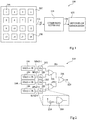
- FIG. 1 schematically illustrates a ranging device 100 according to an example embodiment of the present disclosure.
- the ranging device 100 comprises a SPAD array 102 comprising, in the example of Figure 1 , 16 SPAD devices 104 labelled 1 to 16 and arranged in a four by four grid.
- the output of each SPAD device is provided on a corresponding line of a 16-bit output link 106 to a combining network (COMBINING NETWORK) 118.
- a combining network COMPONING NETWORK
- An output line 120 of the combining network 118 is for example provided to a histogram generation circuit (HISTOGRAM GENERATION) 122, which for example attributes the samples from the SPAD array 102 to different time bins in order to allow the arrival time of a received light pulse, or phase of a received optical waveform, to be determined.
- HISTOGRAM GENERATION histogram generation circuit
- the dynamic range can be increased with respect to the use of only a single SPAD device of the same dimensions.
- the role of the combining network 118 is to condense the outputs from the SPAD devices of the array 102 onto a single output line 120.
- the combining network 118 typically comprises an OR tree for combining the SPAD outputs.
- FIG 2 schematically illustrates the combining network 118 of the ranging device of Figure 1 based on an OR-tree implementation, and according to a simplified example based on the output signals of only four SPAD devices (SPAD + FE) 104 forming the SPAD array 102.
- Each SPAD device for example includes a front end (FE) circuit comprising a MOS transistor for quench/recharge, and an inverter used to re-buffer the leading edge of the SPAD into a digital pulse.
- FE front end
- An output (SPAD 1 to SPAD 4) of each SPAD device 104 is provided to a corresponding pulse shaper (PS) 202, which transforms an event detected by the SPAD device 104 into a pulse of fixed duration.
- the outputs of the pulse shapers 202 are coupled to an OR-tree 204, which comprises three OR gates 206 in the example of Figure 2 , one of the OR gates having its two inputs respectively coupled to the outputs of two of the pulse shapers 202, another of the OR gates having its two inputs respectively coupled to the outputs of the other two pulse shapers 202, and the third OR gate having its two inputs respectively coupled to the outputs of the other two OR gates.
- the output of the third OR gate corresponds to the single output line 120 of the combining network 118.
- Each of the pulse shapers 202 for example has its input coupled to one input of an AND gate 208, and also to the second input of the AND gate 208 via an inverter 210.
- a drawback of the combining network 118 based on the OR tree of Figure 2 is that it suffers from photon pile-up distortion, as will now be described in more detail with reference to Figure 3 .
- Figure 3 is a timing diagram representing signals in the circuit of Figure 2 according to an example embodiment.
- Figure 3 illustrates examples of the output signals SPAD 1 to SPAD 4 of the four SPAD devices 104 of Figure 2 , of a signal OR TREE that would be present at the output of the OR tree 204 in the absence of the pulse shapers 202, and a signal PS+OR TREE corresponding to the signal on the output line 120 of the combining network 118 of Figure 2 .
- a duration tp corresponds to the duration of a pulse on the lines SPAD 1 to SPAD 4 resulting from a SPAD detection event. This pulse duration is reduced to a duration tps by the pulse shapers 202, the dashed lines in the signal PS+OR TREE representing the end of each pulse.
- FIG 4 schematically illustrates the combining network 118 of the ranging device of Figure 1 based on an XOR tree implementation, and according to the same simplified example of Figure 2 based on only four SPAD devices 104 forming the SPAD array 102.
- An output (SPAD 1 to SPAD 4) of each SPAD device (SPAD+FE) 104 is provided to a corresponding toggle device (T) 402, which transforms an event detected by the SPAD device 104 into a binary transition from logic "0" to logic "1” or from logic "1" to logic "0".
- the outputs of the toggle devices 402 are coupled to an XOR tree 404, which comprises three XOR gates 406 in the example of Figure 4 , one of the XOR gates having its two inputs respectively coupled to the outputs of two of the toggle devices 402, another of the XOR gates having its two inputs respectively coupled to the outputs of the other two toggle devices 402, and the third XOR gate having its two inputs respectively coupled to the outputs of the other two XOR gates.
- the output of the third XOR gate corresponds to the single output line 120 of the combining network 118.
- Each of the toggle devices 402 has its input coupled to a clock input of a D-type flip-flop 408, an inverted output Qn of the flip-flop 408 being connected to the data input D of the flip-flop 408.
- the XOR TREE embodiment of Figure 4 can suffer from photon pile-up due to saturation, as will now be described with reference to Figure 5 .
- Figure 5 is a timing diagram representing signals in the circuit of Figure 4 according to an example embodiment.
- Figure 5 illustrates examples of the output signals SPAD 1 to SPAD 4 of the four SPAD devices 104 of Figure 4 , and of a signal XOR TREE corresponding to the signal on the output line 120 of the combining network 118 of Figure 4 .
- a duration tp corresponds to the duration of a pulse on the lines SPAD 1 to SPAD 4 resulting from a SPAD detection event.
- Figure 5 illustrates the same examples of SPAD events 302 to 312 as shown in Figure 3 .
- the SPAD events 302 to 310 cause corresponding transitions 502 to 510 in the output signal, like in the example of Figure 3
- the event 312 is missed, as represented by an arrow 512 without any transition.
- the frequency of the XOR tree increases. High ambient light can therefore lead to very close 0 to 1 to 0 transitions in the XOR tree, leading to events being missed.
- Figure 6 schematically illustrates the combining network of the ranging device of Figure 1 according to an example embodiment of the present disclosure.
- the combining network 118 for example comprises, coupled to the output of each SPAD device 104 forming the SPAD array 102, a corresponding synchronous sampling device 602.
- the synchronous sampling devices 602 are D-type flip-flops all clocked by a clock signal CLK, although other implementations of the synchronous sampling devices 602 would be possible.
- the output signal SST' is for example provided to the data input D of a further L-bit D-type flip-flop 606 clocked by the clock signal CLK, and which provides, at its data output Q, an L-bit output signal SST forming the output of the combining network 118.
- the number N of SPAD devices 104 is for example at least 4.
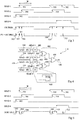
- Figure 7 is a timing diagram representing signals in the circuit of Figure 6 , based on an example of four SPAD devices 104.
- Figure 7 illustrates in particular examples of output signals SPAD 1 to SPAD 4 of the four SPAD devices 104, a series of signals 701 representing pulse additions, and the output signal SST, which is a 4-bit signal in this example (although a 2-bit signal could be used).
- a duration tp in Figure 7 corresponds to the duration of a pulse on the lines SPAD 1 to SPAD 4 resulting from a SPAD detection event. In one embodiment, this duration is equal to around 5 ns, although other durations would be possible.
- the period of the clock signal CLK is for example equal to or less than half the duration tp, and in some embodiments is at least four times shorter than the duration tp.
- the synchronous sampling devices 602 for example sample the signals SPAD 1 to SPAD 4 on each rising edge of the clock signal CLK.
- the generated output pulses have rising and falling edges synchronized with the clock signal CLK.
- These pulses are represented by the signals 701, in which overlapping pulses of the signals SPAD 1 to SPAD 4 are shown stacked, as these pulses will be added by the summation circuit 604.
- the output signal SST thus represents, at each significant edge of the clock signal CLK, the number of signals SPAD 1 to SPAD 4 that is asserted.
- a pulse 702 initially occurs on the signal SPAD 3, causing the signal SST to rise to 1, e.g. a 4-bit binary value of "0001".
- a pulse 704 then occurs shortly thereafter on the signal SPAD 1, causing the signal SST to rise to 2, e.g. a 4-bit binary value of "0010", followed by a pulse 706 on the signal SPAD 2, causing the signal SST to rise to 3, e.g. a 4-bit binary value of "0011".
- the ends of the pulses 702, 704 and 706 then arrive one after the other, respectively causing the output signal SST to fall back to 2, and then to 1, and then to zero.
- a pulse 708 initially occurs on the signal SPAD 1, causing the signal SST to rise to 1, e.g. a 4-bit binary value of "0001".
- a pulse 710 then occurs shortly thereafter on the signal SPAD 2, causing the signal SST to rise to 2, e.g. a 4-bit binary value of "0010", followed by a pulse 712 on the signal SPAD 3, causing the signal SST to rise to 3, e.g. a 4-bit binary value of "0011”.
- a further pulse 714 then occurs on the signal SPAD 1 directly after the pulse 708. However, in view of the sampling of the signal SPAD 1, this pulse 714 having no rising edge is not missed, and causes the signal SST to remain at 3, e.g. the 4-bit binary value of "0011", after the end of the pulse 708.
- the ends of the pulses 710, 712 and 714 then arrive one after the other, respectively causing the output signal SST to fall back to 2, and then to 1, and then to zero.
- Figure 7 illustrates an example according to which the summation circuit 604 only generates output count values when the number of high pulses changes, corresponding to the starts and ends of each pulse of the input signals.
- the summation circuit 604 is configured to generate a count value based on a regular sampling of the SPAD signals, and in particular based on the number of pulses currently asserted, as will now be described in more detail with reference to Figure 8 .
- Figure 8 is a timing diagram representing signals in the circuit of Figure 6 according to continuous synchronous sampling method.
- Figure 8 illustrates the same example of the SPAD output signals SPAD 1, SPAD 2, SPAD 3 and SPAD 4 of Figure 7 , and also illustrates three examples 801, 802 and 803 of the output signal SST based respectively on sampling periods Bin of 500 ps, 1 ns and 2 ns.
- the signals 801, 802 and 803 of Figure 8 use vertical arrows to indicate the output count signal SST at each sampling time.
- the number of generated samples can be reduced in the example of Figure 8 by increasing the sampling period, as represented by the examples 802 and 803, at the expense of reduced precision concerning the pulse timing.
- Figure 9 schematically illustrates the combining network 118 of the ranging device of Figure 1 according to a further example embodiment.
- the embodiment of Figure 9 is similar to that of Figure 6 , except that, rather than being implemented by flip-flops 602, the synchronous sampling devices are implemented by edge detection devices (EDGE DETECT) 902 each of which is clocked by the clock signal CLK.
- EDGE DETECT edge detection devices
- FIG 10 schematically illustrates one of the detection devices 902 of Figure 9 in more detail.
- Each of the devices 902 of Figure 9 is for example implemented by a similar circuit to that of Figure 10 .
- the device 902 for example comprises a flip-flop 1002 having its data input D receiving the corresponding output signal SPADi from one of the SPAD device 104, and its data output Q coupled to the date input D of a further flip-flop 1004.
- the further flip-flop 1004 has its inverted output Qn coupled to one input of an AND gate 1006, the other input of which is coupled to the date output Q of the flip-flop 1002.
- the flip-flops 1002, 1004 are each clocked by the clock signal CLK.
- the edge detection device 902 samples the signals SPADi on each significant edge of the clock signal CLK, but only outputs a high signal when a rising edge is detected.
- the edge detection devices 902 could be modified to detect falling edges by coupling the AND gate input and the data input D of the flip-flop 1004 to an inverted output Qn of the flip-flop 1002 rather that to its data output Q, and by coupling the input of the AND gate 1006 to the data output Q of the flip-flop 1004 rather than to its inverted output Qn.
- Figure 11 is a timing diagram representing signals in the circuit of Figures 9 and 10 according to an example embodiment.
- Figure 11 illustrates the same example of the SPAD output signals SPAD 1, SPAD 2, SPAD 3 and SPAD 4 of Figure 7 , and also illustrates three examples 1101, 1102 and 1103 of different frequencies of the sampling clock signal CLK and of the corresponding output signal SST.
- the sampling periods Bin of the examples 1101, 1102 and 1103 are respectively of 500 ps, 1 ns and 2 ns in the example of Figure 11 .
- the output count value SST corresponds to the number of edges detected during a period of the clock signal CLK.
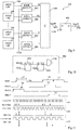
- Figure 12 schematically illustrates the histogram generation circuit 122 of the ranging device of Figure 1 for a dToF implementation according to an example embodiment of the present disclosure, based on the signal SST generated by the summation circuit 604 of Figure 6 or 9 .
- the example of Figure 12 is based on M histogram bins, where M is equal to 8 in the example of Figure 12 .
- the circuit 122 for example comprises a shift-register (SHIFT-REGISTER) 1202 receiving the L-bit values SST, where L is equal to 4 in the example of Figure 12 .
- the shift-register 1202 stores M values of the signal SST, which are shifted at the frequency of the clock signal CLK. Every time that M values have been brought into the shift-register 1202, a load signal LOAD is asserted causing the L-bit value in each of the bins of the shift-register 1202 to be output to a corresponding one of M counters C.
- Each counter C is for example a K-bit counter, and permits a histogram to be generated for J received pulses, where K is for example equal to between 4 and 32, and J is for example equal to at least 10 and typically equal to several hundred.
- the histogram resulting from the cumulative count values of the M counters C can be used to determine an average time-of-flight of the light pulses, and thus determine a range, while also detecting and cancelling cross-talk.
- Figure 13 schematically illustrates a histogram generation circuit of the ranging device of Figure 1 for an iToF implementation according to an example embodiment of the present disclosure, based on the signal SST generated by the summation circuit 604 of Figure 6 or 9 .
- the circuit 122 of Figure 13 is the same as that of Figure 12 , except that the shift-register 1202 of Figure 13 has a number of bins M adapted to the detection of a phase of a waveform.
- the number M of bins can be as low as 2 bins, and in the example of Figure 13 there are 6 bins.
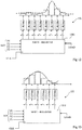
- Figure 14 schematically illustrates an adder tree 1400 for implementing the summation circuit 604 of Figures 6 and 9 according to an example embodiment.
- the example of Figure 14 is based on full adders (FA) and half adders (HA), and on 16 input bits IN(0) to IN(15), which for example correspond to the signals provided by corresponding ones of the flip-flips 602 of Figure 6 or the edge detection devices 902 of Figure 9 .
- Each full adder FA has inputs A and B, a carry input Ci, a sum output S and carry output Co.
- Each half adder HA has inputs A and B, a sum output S, and a carry output Co.
- the adder tree 1400 for example comprises:
- the adder tree 1400 also for example comprises:
- the adder tree 1400 also for example comprises:
- the sum values S 10 , S 12 , S 14 and S 15 for example provide the 4-bit output value OUT(0) to OUT(3) of the adder tree respectively, and the carry value C 15 for example provides a carry output.
- This carry output is for example used as an overflow flag, in which case the number of output bits L is for example equal to log 2 N+1. For example, when asserted, the count value is held at a maximum value, thereby avoiding a case in which the count value will roll-over to zero if the maximum count value is exceeded.
- Figure 15 is a graph representing a detected photon rate as a function of an incident photon rate for four different types of combining networks.
- the photon rates are expressed in counts per second (cps).
- a curve 1502 in Figure 15 represents a simulated detected photon rate based on the OR tree combining network of Figure 2 , but without the pulse shapers 202.
- a curve 1504 in Figure 15 represents a simulated detected photon rate based on the OR tree combining network of Figure 2 with the pulse shapers 202.
- a curve 1506 in Figure 15 represents a simulated detected photon rate based on the combining network of Figure 9 with synchronous sampling devices in the form of edge detection devices 902.
- a curve 1508 in Figure 15 represents a simulated detected photon rate based on the combining network of Figure 6 with synchronous sampling devices in the form of flip-flops 602.
Landscapes
- Engineering & Computer Science (AREA)
- Physics & Mathematics (AREA)
- Computer Networks & Wireless Communication (AREA)
- General Physics & Mathematics (AREA)
- Radar, Positioning & Navigation (AREA)
- Remote Sensing (AREA)
- Electromagnetism (AREA)
- Optical Radar Systems And Details Thereof (AREA)
- Manipulation Of Pulses (AREA)
Priority Applications (2)
| Application Number | Priority Date | Filing Date | Title |
|---|---|---|---|
| EP19180963.1A EP3754367A1 (de) | 2019-06-18 | 2019-06-18 | Schaltung und verfahren zum kombinieren von spad-ausgängen |
| US16/898,600 US11740334B2 (en) | 2019-06-18 | 2020-06-11 | Circuit and method for combining SPAD outputs |
Applications Claiming Priority (1)
| Application Number | Priority Date | Filing Date | Title |
|---|---|---|---|
| EP19180963.1A EP3754367A1 (de) | 2019-06-18 | 2019-06-18 | Schaltung und verfahren zum kombinieren von spad-ausgängen |
Publications (1)
| Publication Number | Publication Date |
|---|---|
| EP3754367A1 true EP3754367A1 (de) | 2020-12-23 |
Family
ID=66998192
Family Applications (1)
| Application Number | Title | Priority Date | Filing Date |
|---|---|---|---|
| EP19180963.1A Withdrawn EP3754367A1 (de) | 2019-06-18 | 2019-06-18 | Schaltung und verfahren zum kombinieren von spad-ausgängen |
Country Status (2)
| Country | Link |
|---|---|
| US (1) | US11740334B2 (de) |
| EP (1) | EP3754367A1 (de) |
Cited By (1)
| Publication number | Priority date | Publication date | Assignee | Title |
|---|---|---|---|---|
| EP4212908A3 (de) * | 2022-01-12 | 2023-09-20 | Samsung Electronics Co., Ltd. | Kollisionswiederherstellung für lidar mit mehreren spad-ereignissen mit geteiltem auslesen |
Families Citing this family (3)
| Publication number | Priority date | Publication date | Assignee | Title |
|---|---|---|---|---|
| US20230353130A1 (en) * | 2022-04-29 | 2023-11-02 | Qrypt, Inc. | Generation of quantum random numbers from single-photon avalanche diodes |
| US20240077592A1 (en) * | 2022-09-07 | 2024-03-07 | Stmicroelectronics (Research & Development) Limited | Carrier modulation ranging using spads |
| CN117516732B (zh) * | 2024-01-08 | 2024-03-12 | 杭州宇称电子技术有限公司 | 基于光子计数的开窗时间可调硅光电倍增器及其控制方法 |
Citations (1)
| Publication number | Priority date | Publication date | Assignee | Title |
|---|---|---|---|---|
| US20180372538A1 (en) * | 2017-06-22 | 2018-12-27 | Denso Corporation | Light detection device |
Family Cites Families (5)
| Publication number | Priority date | Publication date | Assignee | Title |
|---|---|---|---|---|
| US6252428B1 (en) * | 1999-04-07 | 2001-06-26 | Advanced Micro Devices, Inc. | Method and apparatus for detecting a sinusoidal signal |
| JP6017916B2 (ja) * | 2012-10-16 | 2016-11-02 | 株式会社豊田中央研究所 | 光検出器 |
| EP3367131B1 (de) | 2017-02-27 | 2025-08-20 | STMicroelectronics (Research & Development) Limited | Flugzeitsensor mit histogrammauswertung und höherer pixeldichte |
| JP6690660B2 (ja) * | 2017-04-10 | 2020-04-28 | 株式会社デンソー | 光計測装置 |
| CN113748356A (zh) * | 2019-01-18 | 2021-12-03 | 感觉光子公司 | 数字像素及其操作方法 |
-
2019
- 2019-06-18 EP EP19180963.1A patent/EP3754367A1/de not_active Withdrawn
-
2020
- 2020-06-11 US US16/898,600 patent/US11740334B2/en active Active
Patent Citations (1)
| Publication number | Priority date | Publication date | Assignee | Title |
|---|---|---|---|---|
| US20180372538A1 (en) * | 2017-06-22 | 2018-12-27 | Denso Corporation | Light detection device |
Non-Patent Citations (1)
| Title |
|---|
| ALMER OSCAR ET AL: "From linear to geiger mode avalanche detectors for ADC-less VLC receiver architectures", 2017 IEEE PHOTONICS CONFERENCE (IPC), IEEE, 1 October 2017 (2017-10-01), pages 31 - 32, XP033261575, DOI: 10.1109/IPCON.2017.8115992 * |
Cited By (1)
| Publication number | Priority date | Publication date | Assignee | Title |
|---|---|---|---|---|
| EP4212908A3 (de) * | 2022-01-12 | 2023-09-20 | Samsung Electronics Co., Ltd. | Kollisionswiederherstellung für lidar mit mehreren spad-ereignissen mit geteiltem auslesen |
Also Published As
| Publication number | Publication date |
|---|---|
| US11740334B2 (en) | 2023-08-29 |
| US20200400792A1 (en) | 2020-12-24 |
Similar Documents
| Publication | Publication Date | Title |
|---|---|---|
| US11740334B2 (en) | Circuit and method for combining SPAD outputs | |
| US9007118B2 (en) | Circuit for combining signals | |
| CN110622038B (zh) | 光传感器、电子设备、运算装置及对光传感器与检测对象物之间的距离进行测量的方法 | |
| US10890662B2 (en) | Higher pixel density histogram time of flight sensor with higher pixel density | |
| US8432304B2 (en) | Error correction in thermometer codes | |
| US10094915B2 (en) | Wrap around ranging method and circuit | |
| US10416294B2 (en) | Ranging device read-out circuit | |
| US11146270B2 (en) | Proximity sensor and method of operating a photodetector based proximity sensor | |
| US11287518B2 (en) | Optical sensor and electronic device | |
| EP3339985B1 (de) | Zeit-digital-wandler und umwandlungsverfahren | |
| CN112255635A (zh) | 一种距离测量方法、系统及设备 | |
| CN108614255A (zh) | 一种读出电路 | |
| US11982770B2 (en) | Methods and apparatus for histogramming | |
| US10677648B2 (en) | Optical sensor and electronic device | |
| JP2016225876A (ja) | パルス検出回路、放射線検出回路、及び放射線検出装置 | |
| US11592535B2 (en) | Methods and apparatus for repetitive histogramming | |
| US20240210532A1 (en) | Optoelectronic device with time-of-flight sensor using dynamic time windows | |
| US12192661B2 (en) | Image sensors chip with depth information | |
| CN211928162U (zh) | 接近检测设备 | |
| CA3208564A1 (en) | System and method for detection, localization and signaling of single photon events and of at least two photons time coincidence events | |
| WO2023206352A1 (en) | Apparatus for light detection and ranging | |
| US20240201255A1 (en) | Time-to-digtial converter circuit with self-testing function | |
| EP4212908A2 (de) | Kollisionswiederherstellung für lidar mit mehreren spad-ereignissen mit geteiltem auslesen | |
| CN116931000A (zh) | 光学飞行时间传感器、处理电路及方法 | |
| CN119923002A (zh) | 图像传感器 |
Legal Events
| Date | Code | Title | Description |
|---|---|---|---|
| PUAI | Public reference made under article 153(3) epc to a published international application that has entered the european phase |
Free format text: ORIGINAL CODE: 0009012 |
|
| STAA | Information on the status of an ep patent application or granted ep patent |
Free format text: STATUS: THE APPLICATION HAS BEEN PUBLISHED |
|
| AK | Designated contracting states |
Kind code of ref document: A1 Designated state(s): AL AT BE BG CH CY CZ DE DK EE ES FI FR GB GR HR HU IE IS IT LI LT LU LV MC MK MT NL NO PL PT RO RS SE SI SK SM TR |
|
| AX | Request for extension of the european patent |
Extension state: BA ME |
|
| STAA | Information on the status of an ep patent application or granted ep patent |
Free format text: STATUS: THE APPLICATION IS DEEMED TO BE WITHDRAWN |
|
| 18D | Application deemed to be withdrawn |
Effective date: 20210624 |