EP3753111B1 - Digital-analog-wandler und erzeugung von analogen signalen hoher bandbreite - Google Patents
Digital-analog-wandler und erzeugung von analogen signalen hoher bandbreite Download PDFInfo
- Publication number
- EP3753111B1 EP3753111B1 EP19737892.0A EP19737892A EP3753111B1 EP 3753111 B1 EP3753111 B1 EP 3753111B1 EP 19737892 A EP19737892 A EP 19737892A EP 3753111 B1 EP3753111 B1 EP 3753111B1
- Authority
- EP
- European Patent Office
- Prior art keywords
- sub
- stream
- analog
- samples
- digital
- Prior art date
- Legal status (The legal status is an assumption and is not a legal conclusion. Google has not performed a legal analysis and makes no representation as to the accuracy of the status listed.)
- Active
Links
Images


Classifications
-
- H—ELECTRICITY
- H03—ELECTRONIC CIRCUITRY
- H03M—CODING; DECODING; CODE CONVERSION IN GENERAL
- H03M1/00—Analogue/digital conversion; Digital/analogue conversion
- H03M1/06—Continuously compensating for, or preventing, undesired influence of physical parameters
- H03M1/08—Continuously compensating for, or preventing, undesired influence of physical parameters of noise
- H03M1/0836—Continuously compensating for, or preventing, undesired influence of physical parameters of noise of phase error, e.g. jitter
-
- H—ELECTRICITY
- H03—ELECTRONIC CIRCUITRY
- H03M—CODING; DECODING; CODE CONVERSION IN GENERAL
- H03M1/00—Analogue/digital conversion; Digital/analogue conversion
- H03M1/66—Digital/analogue converters
- H03M1/662—Multiplexed conversion systems
-
- H—ELECTRICITY
- H03—ELECTRONIC CIRCUITRY
- H03M—CODING; DECODING; CODE CONVERSION IN GENERAL
- H03M1/00—Analogue/digital conversion; Digital/analogue conversion
- H03M1/66—Digital/analogue converters
- H03M1/74—Simultaneous conversion
- H03M1/76—Simultaneous conversion using switching tree
-
- H—ELECTRICITY
- H04—ELECTRIC COMMUNICATION TECHNIQUE
- H04B—TRANSMISSION
- H04B10/00—Transmission systems employing electromagnetic waves other than radio-waves, e.g. infrared, visible or ultraviolet light, or employing corpuscular radiation, e.g. quantum communication
- H04B10/50—Transmitters
- H04B10/516—Details of coding or modulation
- H04B10/532—Polarisation modulation
-
- H—ELECTRICITY
- H04—ELECTRIC COMMUNICATION TECHNIQUE
- H04B—TRANSMISSION
- H04B10/00—Transmission systems employing electromagnetic waves other than radio-waves, e.g. infrared, visible or ultraviolet light, or employing corpuscular radiation, e.g. quantum communication
- H04B10/50—Transmitters
- H04B10/516—Details of coding or modulation
- H04B10/548—Phase or frequency modulation
- H04B10/556—Digital modulation, e.g. differential phase shift keying [DPSK] or frequency shift keying [FSK]
-
- H—ELECTRICITY
- H04—ELECTRIC COMMUNICATION TECHNIQUE
- H04Q—SELECTING
- H04Q11/00—Selecting arrangements for multiplex systems
- H04Q11/0001—Selecting arrangements for multiplex systems using optical switching
- H04Q11/0005—Switch and router aspects
-
- H—ELECTRICITY
- H04—ELECTRIC COMMUNICATION TECHNIQUE
- H04Q—SELECTING
- H04Q11/00—Selecting arrangements for multiplex systems
- H04Q11/0001—Selecting arrangements for multiplex systems using optical switching
- H04Q11/0005—Switch and router aspects
- H04Q2011/0007—Construction
- H04Q2011/0015—Construction using splitting combining
Definitions
- This disclosure is related to the technical field of generating analog signals and digital-to-analog conversion.
- Ultra-Wideband Digital-to-Analog Conversion Technologies for Tbit/s channel transmission by Yamazaki et al, presented at ECOC 2017 , notes that "high-speed electronic digital-to-analog converters (DACs) are of key importance in modem optical transmission systems" and "in multilevel optical transmitters, the analog bandwidth of the DACs is one of the factors limiting the transmitter's bandwidth”.
- Yamazaki et al. describes a digital-preprocessed analog-multiplexed DAC (DP-AM-DAC) that uses a digital pre-processor, two sub-DACs, and an analog multiplexer (AMUX).
- DP-AM-DAC digital-preprocessed analog-multiplexed DAC
- AMUX analog multiplexer
- the AMUX is a heterojunction bipolar transistor (HBT) analog multiplexer (mux).
- HBT heterojunction bipolar transistor
- Figure 2 of Yamazaki et al. shows an interleaving method (type I) and a preprocessed spectrum method (type II) that reduces the switching frequency of the analog mux by a factor of two.
- type II is very sensitive to imperfections of the matching of the analog characteristics of the two inputs of the analog mux, as very large signal components need to be almost-perfectly cancelled.
- US Patent No. 8,693,876 discloses the combining of two half-band signals from two DACs into a full-band signal, by shifting up the frequency of one of the half-band signals with a bipolar mixer. It is desirable to have the circuit implemented using lower energy technologies such as complementary metal-oxide-semiconductor (CMOS).
- CMOS complementary metal-oxide-semiconductor
- EP3327934A1 discloses an analog multiplexer in combination with digital-to-analog converters for generating a high-speed analog output signal.
- Packet and burst switches are known, where typically 1500 bytes received from one tributary are sent in sequence out of one optical or electrical output.
- Lu et al "Tree-Topology Multiplexer for Multiphase Clock System", IEEE Transactions on Circuits and Systems - I: Regular Papers, vol. 56, no. 1, 1 January 2009 proposes a tree-topology multiplexer (MUX) that employs a multiphase low-frequency clock rather than a high-frequency clock.
- MUX tree-topology multiplexer
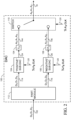
- FIG. 1 illustrates a mechanism for creating a high-bandwidth analog signal.
- a controlled switch 10 has N inputs and a single output, where the number N is equal to three. N sub-streams of analog samples are provided as input to the controlled switch 10, each sub-stream to a respective one of the inputs.
- a first sub-stream 12, a second sub-stream 14 and an N -th sub-stream 16 are illustrated in FIG. 1 .
- the controlled switch 10 is operative to produce a high-bandwidth analog signal at a sample rate of F S .
- the high-bandwidth analog signal comprises an output stream 18 of analog samples ⁇ A 0 , A 1 , A 2 , A 3 , A 4 , A 5 , A 6 , A 7 , ... ⁇ that contains one analog sample in each time period of duration ⁇ T S .
- the symbol " ⁇ " is shorthand for the word "approximately”.
- the index i of each analog sample A i represents an order of the analog samples in the output stream 18.
- a pair of samples is deemed “adjacent” if the index of the second sample in the pair is one greater than the index of the first sample in the pair.
- the controlled switch 10 has N different states. In the first state, the first sub-stream 12 is connected to the output of the controlled switch 10 and thus contributes to the output stream 18. In the second state, the second sub-stream 14 is connected to the output of the controlled switch 10 and thus contributes to the output stream 18. In the N -th state, the N -th sub-stream 16 is connected to the output of the controlled switch 10 and thus contributes to the output stream 18.
- a control signal 20 having a period of ⁇ 2 N T S controls the controlled switch 10 to switch between the N different states.
- the control signal 20 is a clock signal operating at a frequency of 1 2 N F S
- the controlled switch 10 is controlled by rising edges and falling edges of the 1 2 N F S clock signal 20.
- the first sub-stream 12 is intentionally composed of pairs of adjacent analog samples such as ⁇ A 0 , A 1 ⁇ , ⁇ A N , A N+1 ⁇ , and ⁇ A 2N , A 2N+1 ⁇ .
- the timing of the control signal 20 is intentionally arranged so that a data transition occurs between two adjacent analog samples in the first sub-stream 12 while the controlled switch 10 is in the first state.
- the analog samples A 0 and A 1 contribute one after the other to the output stream 18 while the controlled switch 10 is in the first state.
- the second sub-stream 14 is intentionally composed of pairs of adjacent analog samples such as ⁇ A 2 , A 3 ⁇ , ⁇ A N+2 , A N+3 ⁇ , and ⁇ A 2N+2 , A 2N+3 ⁇ .
- the timing of the control signal 20 is intentionally arranged so that a data transition occurs between two adjacent analog samples in the second sub-stream 14 while the controlled switch 10 is in the second state.
- the analog samples A 2 and A 3 contribute one after the other to the output stream 18 while the controlled switch 10 is in the second state.
- the N -th sub-stream 16 is intentionally composed of pairs of adjacent analog samples such as ⁇ A N-2 , A N-1 ⁇ , ⁇ A 2N-2 , A 2N-1 ⁇ , and ⁇ A 3N-2 , A 3N-2 ⁇ .
- the timing of the control signal 20 is intentionally arranged so that a data transition occurs between two adjacent analog samples in the N -th sub-stream 16 while the controlled switch 10 is in the N- th state.
- the analog samples A N-2 and A N-1 contribute one after the other to the output stream 18 while the controlled switch 10 is in the N -th state.
- Two adjacent analog samples in the output stream 18 are substantially determined by a corresponding two adjacent analog samples in one of the sub-streams.
- the output stream 18 has the analog samples ⁇ A 0 , A 1 , A 2 , A 3 , A 4 , A 5 , A 6 , A 7 , ... ⁇ , and the samples ⁇ A 0 , A 1 ⁇ in the output stream 18 are substantially determined by the corresponding samples ⁇ A 0 , A 1 ⁇ in the first sub-stream 12, and the samples ⁇ A 2 , A 3 ⁇ in the output stream 18 are substantially determined by the corresponding samples ⁇ A 2 , A 3 ⁇ in the second sub-stream 14.
- the term "substantially determined” is used to express the fact that the samples in the output stream 18 may not be identical to the samples in the sub-streams. Imperfect circuits may contribute distortion and/or noise. Analog filtering, peaking, hysteresis, reconstruction filtering, and parasitic circuit elements can cause inter-symbol interference (ISI) so that one output sample is a function of more than one input sample, while still being substantially determined by one input sample.
- ISI inter-symbol interference
- One potential benefit of the mechanism described with respect to FIG. 1 is that for a desired sample rate of F S , it is sufficient to generate and bring to the controlled switch 10 a control signal 20 having a period of ⁇ 2 N T S .
- a clock signal 20 operating at ⁇ 1 ⁇ 4F S is sufficient to achieve the desired sample rate of F S .
- a clock signal 20 operating at ⁇ 1 ⁇ 8F S is sufficient to achieve the desired sample rate of F S . It is much easier for the controlled switch 10 to switch when controlled by a slower clock signal than when controlled by a fast clock signal, and the controlled switch 10 will consume less heat when controlled by the slower clock signal than when controlled by the fast clock signal.
- the source of the first sub-stream 12 of analog samples provided as input to the controlled switch 10 is shown conceptually in FIG. 1 as an arbitrary source 22.
- the source of the second sub-stream 14 of analog samples provided as input to the controlled switch 10 is shown conceptually in FIG. 1 as an arbitrary source 24.
- the source of the N -th sub-stream 16 of analog samples provided as input to the controlled switch 10 is shown conceptually in FIG. 1 as an arbitrary source 26.
- FIG. 1 Another potential benefit of the mechanism described with respect to FIG. 1 is that it involves a single control signal 20 to drive the arbitrary sources 22, 24, 26 and to drive the controlled switch 10. No other control signals or clock signals are required.
- Each one of the N sub-streams of analog samples provided as input to the controlled switch 10 may be converted from a respective sub-stream of digital samples (not shown).
- Various example digital-to-analog converters that employ the mechanism described with respect to FIG. 1 are illustrated in FIG. 2 , FIG. 4 , FIG. 6 , and FIG. 8 and are described hereinbelow.
- the arbitrary sources 22, 24, 26 of the N sub-streams of analog samples are sub-DACs controlled by a clock signal operating at a frequency of 1 2 N F S .
- Linear digital filtering of the sub-streams of digital samples may adapt the signals in each sub-stream to obtain a cleaner output from the controlled switch 10. This may become more important when the controlled switch 10 is physically further away from the sources of the sub-streams.
- the linear digital filtering may be calibrated in the factory. Alternatively, local or remote feedback may be used to dynamically control the linear digital filtering.
- Nonlinear compensation may be included in the generation of the sub-streams, for example, as described in US Patent No. 6781537 to Taraschuk et al. , without memory, or with memory (time delays) in the response. This nonlinear compensation may compensate for nonlinearity in the component DACs, the controlled switch, or downstream elements.
- the arrangement of the timing of the control signal 20 relative to the occurrence of data transitions between two adjacent analog samples in the sub-streams may result from delays introduced in the sub-streams. This is the case, for example, in the DACs illustrated in FIG. 2 and FIG. 6 .
- the arrangement of the timing of the control signal 20 relative to the occurrence of data transitions between two adjacent analog samples in the sub-streams may result from a phase offset between the control signal 20 and clocks used to generate the sub-streams. This is the case, for example, in the DACs illustrated in FIG. 4 and FIG. 8 .
- Phase shifting may be used to obtain precision control of the clock phases. This may be calibrated in the factory. Alternatively, local or remote feedback may be used to dynamically control the phase.
- FIG. 2 illustrates an example digital-to-analog converter (DAC) 100, not forming part of the claimed invention, that is operative to convert an input stream 102 of digital samples ⁇ D 0 , D 1 , D 2 , D 3 , ... ⁇ into the output stream 18 of analog samples ⁇ A 0 , A 1 , A 2 , A 3 , ... ⁇ at a sampling rate of F S .
- DAC digital-to-analog converter
- FIG. 3 is a timing diagram of clock signals and data signals in the DAC 100.
- the DAC 100 comprises a "positive" sub-DAC component 104, a “negative” sub-DAC component 106, and a controlled switch 110.
- the controlled switch 110 has two inputs (coupled to the outputs of the sub-DAC components 104, 106) and a single output (the output stream 18).
- the positive sub-DAC component 104 receives as input a first sub-stream 114 of digital samples ⁇ D 0 , D 1 , D 4 , D 5 , ... ⁇
- the negative sub-DAC component 106 receives as input a second sub-stream 116 of digital samples ⁇ D 2 , D 3 , D 6 , D 7 , ... ⁇ .
- the first sub-stream 114 is composed of pairs of adjacent digital samples such as ⁇ D 0 , D 1 ⁇ , ⁇ D 4 , D 5 ⁇ , and ⁇ D 8 , D 9 ⁇
- the second sub-stream 116 is composed of pairs of adjacent digital samples such as ⁇ D 2 , D 3 ⁇ , ⁇ D 6 , D 7 ⁇ , and ⁇ D 10 , D 11 ⁇ .
- a partitioning module 112 comprised in the DAC 100 is operative to partition the input stream 102 of digital samples into the first sub-stream 114 and the second sub-stream 116, using any suitable technique.
- the partitioning module 112 could reorder every four consecutive samples in the input stream 102 as ⁇ D 0 , D 2 , D 1 , D 3 , D 4 , D 6 , D 5 , D 7 , ... ⁇ .
- the partitioning module 112 could apply a decimate-by-two function to the reordered samples.
- the partitioning module 112 could delay a copy of the reordered samples by a delay of duration ⁇ T S , and then apply a decimate-by-two function.
- a clock signal 120 operating at ⁇ 1 ⁇ 4F S (and therefore having a period of ⁇ 4T S ) is provided to the sub-DAC components 104, 106.
- the positive sub-DAC component 104 samples the first sub-stream 114 at rising edges and falling edges of the ⁇ 1 ⁇ 4F S clock signal 120, thus converting the first sub-stream 114 into a first sub-stream 124 of analog samples ⁇ A 0 , A 1 , A 4 , A 5 , ... ⁇ .
- the negative sub-DAC component 106 samples the second sub-stream 116 at rising edges and falling edges of the ⁇ 1 ⁇ 4F S clock signal 120, thus converting the second sub-stream 116 into a second sub-stream 126 of analog samples ⁇ A 2 , A 3 , A 6 , A 7 , ... ⁇ .
- An analog delay line 134 is operative to delay the first sub-stream 124 by a delay of duration ⁇ T S , yielding a first sub-stream 144 of delayed analog samples ⁇ A 0 , A 1 , A 4 , A 5 , ... ⁇ .
- An analog delay line 136 is operative to delay the second sub-stream 126 by a delay of duration ⁇ 3T S , yielding a second sub-stream 146 of delayed analog samples ⁇ A 2 , A 3 , A 6 , A 7 , ... ⁇ .
- the first sub-stream 144 is a specific example of the first sub-stream 12 described with respect to FIG. 1
- the second sub-stream 146 is a specific example of the second sub-stream 14 described with respect to FIG. 1 .
- the ⁇ 1 ⁇ 4F S clock signal 120 is provided, with zero phase offset, to the controlled switch 110.
- the controlled switch 110 is controlled by rising edges and falling edges of the ⁇ 1 ⁇ 4F S clock signal 120, switching between a "positive" state in which the first sub-stream 144 of delayed analog samples ⁇ A 0 , A 1 , A 4 , A 5 , ... ⁇ contributes to the output stream 18 and a "negative" state in which the second sub-stream 146 of delayed analog samples ⁇ A 2 , A 3 , A 6 , A 7 , ... ⁇ contributes to the output stream 18.
- the resulting output stream 18 of analog samples ⁇ A 0 , A 1 , A 2 , A 3 , A 4 , A 5 , A 6 , A 7 , ... ⁇ contains one analog sample in each time period of duration ⁇ T S .
- analog delay line 134 and the analog delay line 136 are operative to introduce delays in the sub-streams of analog samples. These delays result in the arrangement of the timing of the "positive" states and “negative” states of the controlled switch 110 relative to the occurrence of data transitions between two adjacent analog samples in the first sub-stream 144 and in the second sub-stream 146.
- the controlled switch 110 While the controlled switch 110 is in the "positive” state, the data transition in the first sub-stream 144 from one analog sample to an adjacent analog sample is captured. While the controlled switch 110 is in the "negative” state, the data transition in the second sub-stream 146 from one analog sample to an adjacent analog sample is captured.
- the analog samples A 0 and A 1 contribute one after the other to the output stream 18 during a single half-period of duration ⁇ 2T S of the ⁇ 1 ⁇ 4F S clock signal 120
- the analog samples A 2 and A 3 contribute one after the other to the output stream 18 during a next single half-period of duration ⁇ 2T S of the ⁇ 1 ⁇ 4F S clock signal 120.
- the DAC 100 produces the output stream 18 at the rate of ⁇ F S using clock signals operating solely at ⁇ 1 ⁇ 4F S .
- FIG. 4 illustrates an example digital-to-analog converter (DAC) 150, not forming part of the claimed invention, that is operative to convert the input stream 102 of digital samples ⁇ D 0 , D 1 , D 2 , D 3 , ... ⁇ into the output stream 18 of analog samples ⁇ A 0 , A 1 , A 2 , A 3 , ... ⁇ at the sampling rate of F S .
- DAC digital-to-analog converter
- FIG. 5 is a timing diagram of clock signals and data signals in the DAC 150.
- the DAC 150 is a variant of the DAC 100 illustrated in FIG. 2 . In contrast to the DAC 100, there are no analog delay lines in the DAC 150. (The first sub-stream 124 is a specific example of the first sub-stream 12 described with respect to FIG. 1 , and the second sub-stream 126 is a specific example of the second sub-stream 14 described with respect to FIG. 1 .)
- the ⁇ 1 ⁇ 4F S clock signal 120 provided to the controlled switch 110 has a 90° phase offset relative to the ⁇ 1 ⁇ 4F S clock signal 120 that is provided to the sub-DAC components 104, 106.
- the controlled switch 110 is controlled by rising edges and falling edges of the 90° phase offset ⁇ 1 ⁇ 4F S clock signal 120, switching between a "positive" state in which the first sub-stream 124 of analog samples ⁇ A 0 , A 1 , A 4 , A 5 , ... ⁇ contributes to the output stream 18 and a "negative" state in which the second sub-stream 126 of analog samples ⁇ A 2 , A 3 , A 6 , A 7 , ... ⁇ contributes to the output stream 18.
- the resulting output stream 18 of analog samples ⁇ A 0 , A 1 , A 2 , A 3 , A 4 , A 5 , A 6 , A 7 , ... ⁇ contains one analog sample in each time period of duration ⁇ T S .
- the ⁇ 1 ⁇ 4F S clock signal 120 provided to the controlled switch 110 has a 90° phase offset relative to the ⁇ 1 ⁇ 4F S clock signal 120 that is provided to the sub-DAC components 104, 106.
- This 90° phase offset results in the arrangement of the timing of the "positive” states and “negative” states of the controlled switch 110 relative to the occurrence of data transitions between two adjacent analog samples in the first sub-stream 124 and in the second sub-stream 126.
- the controlled switch 110 While the controlled switch 110 is in the "positive” state, the data transition in the first sub-stream 124 from one analog sample to an adjacent analog sample is captured. While the controlled switch 110 is in the "negative” state, the data transition in the second sub-stream 126 from one analog sample to an adjacent analog sample is captured.
- the analog samples A 0 and A 1 contribute one after the other to the output stream 18 during a single half-period of duration ⁇ 2T S of the 90° phase offset ⁇ 1 ⁇ 4F S clock signal 120
- the analog samples A 2 and A 3 contribute one after the other to the output stream 18 during a next single half-period of duration ⁇ 2T S of the 90° phase offset ⁇ 1 ⁇ 4F S clock signal 120.
- the DAC 150 produces the output stream 18 at the rate of ⁇ F S using clock signals operating solely at ⁇ 1 ⁇ 4F S .
- FIG. 6 illustrates an example digital-to-analog converter (DAC) 200 that is operative to convert the input stream 102 of digital samples ⁇ D 0 , D 1 , D 2 , D 3 , ... ⁇ into the output stream 18 of analog samples ⁇ A 0 , A 1 , A 2 , A 3 , ... ⁇ at the sampling rate of F S .
- DAC digital-to-analog converter
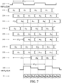
- FIG. 7 is a timing diagram of clock signals and data signals in the DAC 200.
- the DAC 200 comprises a "positive" sub-DAC component 204, a "zero” sub-DAC component 206, a “negative” sub-DAC component 208, and a controlled switch 210.
- the controlled switch 210 has three inputs (coupled to the outputs of the sub-DAC components 204, 206, 208) and a single output (the output stream 18).
- the positive sub-DAC component 204 receives as input a first sub-stream 214 of digital samples ⁇ D 0 , D 1 , D 6 , D 7 , ... ⁇
- the zero sub-DAC component 206 receives as input a second sub-stream 216 of digital samples ⁇ D 2 , D 3 , D 8 , D 9 , ... ⁇
- the negative sub-DAC component 208 receives as input a third sub-stream 218 of digital samples ⁇ D 4 , D 5 , D 10 , D 11 , ... ⁇ .
- the first sub-stream 214 is composed of pairs of adjacent samples such as ⁇ D 0 , D 1 ⁇ , ⁇ D 6 , D 7 ⁇ , and ⁇ D 12 , D 13 ⁇
- the second sub-stream 216 is composed of pairs of adjacent samples such as ⁇ D 2 , D 3 ⁇ , ⁇ D 8 , D 9 ⁇ , and ⁇ D 14 , D 15 ⁇
- the third sub-stream 218 is composed of pairs of adjacent samples such as ⁇ D 4 , D 5 ⁇ , ⁇ D 10 , D 11 ⁇ , and ⁇ D 16 , D 17 ⁇ .
- a partitioning module 212 comprised in the DAC 200 is operative to partition the input stream 102 of digital samples into the first sub-stream 214, the second sub-stream 216, and the third sub-stream 218, using any suitable technique.
- a clock signal 220 operating at ⁇ 1 6 F S (and therefore having a period of ⁇ 6T S ) is provided to the sub-DAC components 204, 206, 208.
- the positive sub-DAC component 204 samples the first sub-stream 214 at rising edges and falling edges of the ⁇ 1 6 F S clock signal 220, thus converting the first sub-stream 214 into a first sub-stream 224 of analog samples ⁇ A 0 , A 1 , A 6 , A 7 , ... ⁇ .
- the zero sub-DAC component 206 samples the second sub-stream 216 at rising edges and falling edges of the ⁇ 1 6 F S clock signal 220, thus converting the second sub-stream 216 into a second sub-stream 226 of analog samples ⁇ A 2 , A 3 , A 8 , A 9 , ... ⁇ .
- the negative sub-DAC component 208 samples the third sub-stream 218 at rising edges and falling edges of the ⁇ 1 6 F S clock signal 220, thus converting the third sub-stream 218 into a third sub-stream 228 of analog samples ⁇ A 4 , A 5 , A 10 , A 11 , ... ⁇ .
- An analog delay line 234 is operative to delay the first sub-stream 224 by a delay of duration ⁇ T S , yielding a first sub-stream 244 of delayed analog samples ⁇ A 0 , A 1 , A 6 , A 7 , ... ⁇ .
- An analog delay line 236 is operative to delay the second sub-stream 226 by a delay of duration ⁇ 3T S , yielding a second sub-stream 246 of delayed analog samples ⁇ A 2 , A 3 , A 8 , A 9 , ... ⁇ .
- An analog delay line 238 is operative to delay the third sub-stream 228 by a delay of duration ⁇ 5T S , yielding a third sub-stream 248 of delayed analog samples ⁇ A 4 , A 5 , A 10 , A 11 , ... ⁇ .
- a three-state control signal 240 having a period of ⁇ 6T S is provided to the controlled switch 210.
- the controlled switch 210 is controlled by transitions of the three-state control signal 240, switching between a "positive" state in which the first sub-stream 244 of delayed analog samples ⁇ A 0 , A 1 , A 6 , A 7 , ... ⁇ contributes to the output stream 18, a "zero" state in which the second sub-stream 246 of delayed analog samples ⁇ A 2 , A 3 , A 8 , A 9 , ... ⁇ contributes to the output stream 18, and a "negative" state in which the third sub-stream 248 of delayed analog samples ⁇ A 4 , A 5 , A 10 , A 11 , ... ⁇ contributes to the output stream 18.
- the resulting output stream 18 of analog samples ⁇ A 0 , A 1 , A 2 , A 3 , A 4 , A 5 , A 6 , A 7 , ... ⁇ contains one analog sample in each time period of duration
- the three-state control signal 240 has a zero-phase offset relative to the ⁇ 1 6 F S clock signal 220 provided to the sub-DAC components 204, 206, 208.
- the delays introduced by the analog delay lines 234, 236, and 238 result in the arrangement of the timing of the "positive”, “zero” and “negative” states of the controlled switch 210, respectively, relative to the occurrence of data transitions between two adjacent analog samples in the first sub-stream 244, the second sub-stream 246 and the third sub-stream 248.
- While the controlled switch 210 is in the "positive” state, the data transition in the first sub-stream 244 from one analog sample to an adjacent analog sample is captured. While the controlled switch 210 is in the "zero” state, the data transition in the second sub-stream 246 from one analog sample to an adjacent analog sample is captured. While the controlled switch 210 is in the "negative” state, the data transition in the third sub-stream 248 from one analog sample to an adjacent analog sample is captured.
- the analog samples A 0 and A 1 contribute one after the other to the output stream 18 during a single third-period of duration ⁇ 2T S of the control signal 240, and then the analog samples A 2 and A 3 contribute one after the other to the output stream 18 during a next single third-period of duration ⁇ 2T S of the control signal 240, and then the analog samples A 4 and A 5 contribute one after the other to the output stream 18 during a next single third-period of duration ⁇ 2T S of the control signal 240.
- the DAC 200 produces the output stream at the rate of ⁇ F S using clock signals operating solely at ⁇ 1 6 F S .
- FIG. 8 illustrates an example digital-to-analog converter (DAC) 250 that is operative to convert the input stream 102 of digital samples ⁇ D 0 , D 1 , D 2 , D 3 , ... ⁇ into the output stream 18 of analog samples ⁇ A 0 , A 1 , A 2 , A 3 , ... ⁇ at the sampling rate of F S .
- DAC digital-to-analog converter
- FIG. 9 is a timing diagram of clock signals and data signals in the DAC 250.
- the DAC 250 is a variant of the DAC 200 illustrated in FIG. 5 . In contrast to the DAC 200, there are no analog delay lines in the DAC 250.
- a three-state control signal 260 having a period of ⁇ 6T S is provided to the controlled switch 210.
- the controlled switch 210 is controlled by transitions of the three-state control signal 260, switching between a "positive" state in which the first sub-stream 224 of analog samples ⁇ A 0 , A 1 , A 6 , A 7 , ... ⁇ contributes to the output stream 18, a "zero" state in which the second sub-stream 226 of analog samples ⁇ A 2 , A 3 , A 8 , A 9 , ... ⁇ contributes to the output stream 18, and a "negative" state in which the third sub-stream 228 of analog samples ⁇ A 4 , A 5 , A 10 , A 11 , ...
- the resulting output stream 18 of analog samples ⁇ A 0 , A 1 , A 2 , A 3 , A 4 , A 5 , A 6 , A 7 , ... ⁇ contains one analog sample in each time period of duration ⁇ T S .
- the three-state control signal 260 has a 60° phase offset relative to the ⁇ 1 6 F S clock signal 220.
- This 60° phase offset results in the arrangement of the timing of the "positive”, “zero” and “negative” states of the controlled switch 210 relative to the occurrence of data transitions between two adjacent analog samples in the first sub-stream 224, the second sub-stream 226 and the third sub-stream 228.
- While the controlled switch 210 is in the "positive” state, the data transition in the first sub-stream 224 from one analog sample to an adjacent analog sample is captured. While the controlled switch 210 is in the "zero” state, the data transition in the second sub-stream 226 from one analog sample to an adjacent analog sample is captured. While the controlled switch 210 is in the "negative” state, the data transition in the third sub-stream 228 from one analog sample to an adjacent analog sample is captured.
- the analog samples A 0 and A 1 contribute one after the other to the output stream 18 during a single third-period of duration ⁇ 2T S of the three-state control signal 260, and then the analog samples A 2 and A 3 contribute one after the other to the output stream 18 during a next single third-period of duration ⁇ 2T S of the three-state control signal 260, and then the analog samples A 4 and A 5 contribute one after the other to the output stream 18 during a next single third-period of duration ⁇ 2T S of the three-state control signal 260.
- the DAC 250 produces the output stream 18 at the rate of ⁇ F S using clock signals operating solely at ⁇ 1 6 F S .
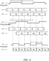
- FIG. 10 illustrates an example sub-DAC 300, not forming part of the claimed invention, that is operative to convert digital samples into analog samples.
- the sub-DAC 300 may optionally be used as the "positive" sub-DAC 104 in DAC 100 or DAC 150 to convert the first sub-stream 114 of digital samples ⁇ D 0 , D 1 , D 4 , D 5 , ... ⁇ into the first sub-stream 124 of analog samples ⁇ A 0 , A 1 , A 4 , A 5 , ... ⁇ at a sampling rate of 1 ⁇ 2F S .
- FIG. 11 is a timing diagram of clock signals and data signals in the sub-DAC 300.
- the sub-DAC 300 comprises an "even" sub-sub-DAC component 304, an "odd” sub-DAC component 306, and an analog multiplexer (AMUX) component 310.
- the AMUX component 310 has two inputs (coupled to the outputs of the sub-sub-DAC components 304, 306) and a single output (the first sub-stream 124).
- the even sub-sub-DAC component 304 receives as input a first sub-sub-stream 314 of digital samples ⁇ D 0 , D 4 , D 8 , ... ⁇
- the odd sub-sub-DAC component 306 receives as input a second sub-sub-stream 316 of digital samples ⁇ D 1 , D 5 , D 9 , ... ⁇ .
- a partitioning module 312 is operative to partition the first sub-stream 114 of digital samples into the first sub-sub-stream 314 and the second sub-sub-stream 316, using any suitable technique.
- the first sub-stream 114 could be duplicated, a delay buffer (not shown) could delay one copy of the first sub-stream 114 by a duration of ⁇ T S , and decimator elements (not shown) could remove every other sample from the copies of the first sub-stream 114.
- a clock signal 320 operating at ⁇ 1 ⁇ 8F S (and therefore having a period of ⁇ 8T S ) is provided to the sub-sub-DAC components 304, 306.
- the ⁇ 1 ⁇ 8F S clock signal 320 provided to the odd sub-sub-DAC component 306 has a 90° phase offset relative to the ⁇ 1 ⁇ 8F S clock signal 320 provided to the even sub-sub-DAC component 304.
- the even sub-sub-DAC component 304 samples the first sub-sub-stream 314 at rising edges and falling edges of the ⁇ 1 ⁇ 8F S clock signal 320, thus converting the first sub-sub-stream 314 into a first sub-sub-stream 324 of analog samples ⁇ A 0 , A 4 , A 8 , ... ⁇ .
- the odd sub-DAC component 306 samples the second sub-sub-stream 316 at rising edges and falling edges of the 90° phase offset ⁇ 1 ⁇ 8F S clock signal 320, thus converting the second sub-sub-stream 316 into a second sub-sub-stream 326 of analog samples ⁇ A 1 , A 5 , A 9 , ... ⁇ .
- the ⁇ 1 ⁇ 4F S clock signal 120 is provided to the AMUX component 310.
- the AMUX component 310 is controlled by rising edges and falling edges of the ⁇ 1 ⁇ 4F S clock signal 120, switching between an "even" state in which the first sub-sub-stream 324 of analog samples ⁇ A 0 , A 4 , A 8 , ... ⁇ contributes a single analog sample to the first sub-stream 124 and an "odd" state in which the second sub-sub-stream 326 of analog samples ⁇ A 1 , A 5 , A 9 , ... ⁇ contributes a single analog sample to the first sub-stream 124.
- the resulting first sub-stream 124 of analog samples ⁇ A 0 , A 1 , A 4 , A 5 , A 8 , A 9 , ... ⁇ contains one analog sample in each time period of duration ⁇ 2T S .
- the ⁇ 1 ⁇ 4F S clock signal 120 is offset by approximately 90° phase from double the ⁇ 1 ⁇ 8F S clock signal 320.
- the ⁇ 1 ⁇ 4F S clock signal 120 is intentionally timed so that no data transition occurs between analog samples in the first sub-sub-stream 324 while the AMUX component 310 is in the "even” state, and no data transition occurs between analog samples in the second sub-sub-stream 326 while the AMUX component 310 is in the "odd” state. Stated differently, all samples in the first sub-stream 124 are captured from stable portions of the sub-sub-streams 324 and 326.
- FIG. 12 illustrates an example sub-DAC 350, not forming part of the claimed invention, that is operative to convert digital samples into analog samples.
- the sub-DAC 350 may optionally be used as the "negative" sub-DAC 106 in DAC 100 or DAC 150 to convert the second sub-stream 116 of digital samples ⁇ D 2 , D 3 , D 6 , D 7 , ... ⁇ into the second sub-stream 126 of analog samples ⁇ A 2 , A 3 , A 6 , A 7 , ... ⁇ at a sampling rate of 1 ⁇ 2F S .
- FIG. 13 is a timing diagram of clock signals and data signals in the sub-DAC 350.
- the sub-DAC 350 comprises an "even" sub-sub-DAC component 354, an "odd” sub-DAC component 356, and an analog multiplexer (AMUX) component 360.
- the AMUX component 360 has two inputs (coupled to the outputs of the sub-sub-DAC components 354, 356) and a single output (the second sub-stream 126).
- the even sub-sub-DAC component 354 receives as input a first sub-sub-stream 364 of digital samples ⁇ D 2 , D 6 , D 10 , ... ⁇
- the odd sub-sub-DAC component 356 receives as input a second sub-sub-stream 366 of digital samples ⁇ D 3 , D 7 , D 11 , ... ⁇ .
- a partitioning module 362 is operative to partition the second sub-stream 116 of digital samples into the first sub-sub-stream 364 and the second sub-sub-stream 366, using any suitable technique.
- the second sub-stream 116 could be duplicated, a delay buffer (not shown) could delay one copy of the second sub-stream 116 by a duration of ⁇ T S , and decimator elements (not shown) could remove every other sample from the copies of the second sub-stream 116.
- the ⁇ 1 ⁇ 8F S clock signal 320 is provided to the sub-sub-DAC components 354, 356.
- the ⁇ 1 ⁇ 8F S clock signal 320 provided to the odd sub-sub-DAC component 356 has a 90° phase offset relative to the ⁇ 1 ⁇ 8F S clock signal 320 provided to the even sub-sub-DAC component 354.
- the even sub-sub-DAC component 354 samples the first sub-sub-stream 364 at rising edges and falling edges of the 90° phase offset ⁇ 1 ⁇ 8F S clock signal 320, thus converting the first sub-sub-stream 364 into a first sub-sub-stream 374 of analog samples ⁇ A 2 , A 6 , A 10 , ... ⁇ .
- the odd sub-DAC component 356 samples the second sub-sub-stream 366 at rising edges and falling edges of the ⁇ 1 ⁇ 8F S clock signal 320, thus converting the second sub-sub-stream 366 into a second sub-sub-stream 376 of analog samples ⁇ A 3 , A 7 , A 11 , ... ⁇ .
- the ⁇ 1 ⁇ 4F S clock signal 120 is provided to the AMUX component 360.
- the AMUX component 360 is controlled by rising edges and falling edges of the ⁇ 1 ⁇ 4F S clock signal 120, switching between an "even" state in which the first sub-sub-stream 374 of analog samples ⁇ A 2 , A 6 , A 10 , ... ⁇ contributes a single analog sample to the second sub-stream 126 and an "odd" state in which the second sub-sub-stream 376 of analog samples ⁇ A 3 , A 7 , A 11 , ... ⁇ contributes a single analog sample to the second sub-stream 126.
- the resulting second sub-stream 126 of analog samples ⁇ A 2 , A 3 , A 6 , A 7 , A 10 , A 11 , ... ⁇ contains one analog sample in each time period of duration ⁇ 2T S .
- the ⁇ 1 ⁇ 4F S clock signal 120 is offset by approximately 90° phase from double the ⁇ 1 ⁇ 8F S clock signal 320.
- the ⁇ 1 ⁇ 4F S clock signal 120 is intentionally timed so that no data transition occurs between analog samples in the first sub-sub-stream 374 while the AMUX component 360 is in the "even” state, and no data transition occurs between analog samples in the second sub-sub-stream 376 while the AMUX component 360 is in the "odd” state. Stated differently, all samples in the second sub-stream 126 are captured from stable portions of the sub-sub-streams 374 and 376.
- the increased complexity involves providing a clock signal at approximately one quarter of the sampling rate ( ⁇ 1 ⁇ 4F S ), and the increased complexity may be deemed acceptable.
- Sub-DACs similar to the sub-DACs 300 and 350 could be used as the "positive" sub-DAC, "zero” sub-DAC, and “negative” sub-DAC in the DAC 200 or in the DAC 250.
- FIG. 14 is a block diagram illustration of an example transmitter 400 that employs polarization-division multiplexing (PDM).
- a laser 402 is operative to generate a continuous wave (CW) optical carrier 404.
- a polarizing beam splitter 406 is operative to split the CW optical carrier 404 into orthogonally-polarized components 408, 410 (nominally referred to as the "X-polarization” component and the "Y-polarization” component) that are modulated by respective electrical-to-optical modulators 412, 414 to produce modulated polarized optical signals 416, 418 that are combined by a beam combiner 420, thus yielding an optical signal 422.
- a symbol source 424 is operative to generate a stream of symbols representing data to be transmitted in the optical signal 422.
- a digital signal processor (DSP) 426 is operative to process the symbols output from the symbol source 424, for example, performing one or more of pulse shaping, subcarrier multiplexing, chromatic dispersion pre-compensation, and distortion pre-compensation on the symbols.
- the DSP 426 is operative to generate I and Q digital drive signals 432 for the X-polarization to be converted by a DAC 434 into I and Q analog drive signals 436 for the X-polarization that, after amplification by amplifiers 438, are used to drive the electrical-to-optical modulator 412.
- the DSP 426 is operative to generate I and Q digital drive signals 442 for the Y-polarization to be converted by a DAC 444 into I and Q analog drive signals 446 for the Y-polarization that, after amplification by amplifiers 448, are used to drive the electrical-to-optical modulator 414.
- the I and Q digital drive signals 432 for the X-polarization may be the input stream 102 of digital samples ⁇ D 0 , D 1 , D 2 , D 3 , ... ⁇ and the I and Q analog drive signals 436 for the X-polarization may be the output stream 18 of analog samples ⁇ A 0 , A 1 , A 2 , A 3 , ... ⁇ .
- the I and Q digital drive signals 442 for the Y-polarization may be the input stream 102 of digital samples ⁇ D 0 , D 1 , D 2 , D 3 , ... ⁇ and the I and Q analog drive signals 446 for the Y-polarization may be the output stream 18 of analog samples ⁇ A 0 , A 1 , A 2 , A 3 , ... ⁇ .
- each of the DAC 434, 444 may comprise two or more sub-DACs, and the streams of analog samples that are output from the two or more sub-DACs may be provided as inputs to a controlled switch that is a specific example of the controlled switch 10 described with respect to FIG. 1 .
- a sub-DAC may employ the architecture described with respect to FIG. 10 or FIG. 12 .
- the DSP 426 and the DACs 434, 444 are comprised in a CMOS module, and the amplifiers 438, 448 are comprised in a BiCMOS module.
- the controlled switches of the DACs 434, 444 may be separate from the CMOS module that comprises the DSP 426 and the other components (including the sub-DACs) of the DACs 434, 444.
- the controlled switches may be comprised in another CMOS module, or a BiCMOS module, or HBT.
- the controlled switches may be co-packaged with the electrical-to-optical modulator 412, 414 or the driver.
- the controlled switch may be implemented with nonlinear electrical, electro-optic, or optical elements, such as CMOS field effect transistors (FETs) or diodes, bipolar transistors or diodes, heterojunction bipolar transistors (HBTs), electro-absorption (EA) modulators, phase modulators, or semiconductor optical amplifier (SOA) structures.
- FETs CMOS field effect transistors
- HBTs bipolar transistors or diodes
- EA electro-absorption
- SOA semiconductor optical amplifier
- the switching function may be substantially a multiplication by the clock voltage or may include strong nonlinear functional terms.
- CMOS complementary metal-oxide-semiconductor
- current sub-streams may be converted to an optical E-Field stream, as was described in US Patent No. 7277603 to Roberts et al.
- An integer sub-stream may be combined with a voltage sub-stream to produce a voltage stream.
- the analog characteristic of the stream that is being created may be an optical or electrical phase, or other modulation of an input analog signal.
- a series of integer values that represent a time-series signal may be instantiated in parallel circuits or any other pre-determined pattern.
Landscapes
- Engineering & Computer Science (AREA)
- Theoretical Computer Science (AREA)
- Computer Networks & Wireless Communication (AREA)
- Physics & Mathematics (AREA)
- Electromagnetism (AREA)
- Signal Processing (AREA)
- Analogue/Digital Conversion (AREA)
Claims (5)
- Verfahren, umfassend:Aufteilen eines Eingangsstroms (102) von digitalen Abtastwerten {D0, D1, D2, D3, ...} in N Teilströme (114, 116, 214, 216, 218), wobei N drei ist, sodass der erste Teilstrom ein erstes Paar benachbarter digitaler Abtastwerte {D0, D1} aus dem Eingangsstrom und jedes nachfolgende N-te Paar benachbarter digitaler Abtastwerte {D2N, D2N+1} aus dem Eingangsstrom beinhaltet, und der zweite Teilstrom ein zweites Paar benachbarter digitaler Abtastwerte {D2, D3} aus dem Eingangsstrom und jedes nachfolgende N-te Paar benachbarter digitaler Abtastwerte {D2n+2, D2N+3} aus dem Eingangsstrom beinhaltet;für jeden der N TeilströmeUmwandeln des Teilstroms digitaler Abtastwerte in einen jeweiligen Teilstrom (124, 126, 224, 226, 228) analoger Abtastwerte, sodass jeder analoge Abtastwert in dem Teilstrom analoger Abtastwerte aus einem stabilen Abschnitt eines entsprechenden digitalen Abtastwerts in dem Teilstrom digitaler Abtastwerte erfasst wird, und wobei der Teilstrom analoger Abtastwerte einen analogen Abtastwert in jedem Zeitraum der Dauer ~2Ts enthält; undBereitstellen des Teilstroms analoger Abtastwerte an einen entsprechenden von N Eingängen eines gesteuerten Schalters (110, 210), wobei der gesteuerte Schalter einen einzigen Ausgang aufweist; undSteuern des gesteuerten Schalters mit einem Steuersignal, um zwischen N verschiedenen Zuständen umzuschalten, wobei das Steuersignal eine Periode von ~2NTs aufweist, wobei in jedem Zustand jeweils einer der N Eingänge mit dem einzigen Ausgang verbunden ist,wobei, während sich der gesteuerte Schalter in einem der N verschiedenen Zustände befindet, ein Datenübergang zwischen zwei benachbarten analogen Abtastwerten in dem Teilstrom stattfindet, der dem einen der N Eingänge bereitgestellt wird, der mit dem einzigen Ausgang verbunden ist,wobei der einzige Ausgang ein analoges Signal (18) mit hoher Bandbreite liefert, das einen analogen Abtastwert {A0, A1, A2, A3, ...} in jedem Zeitraum der Dauer von ungefähr Ts enthält, und jedes Paar benachbarter analoger Abtastwerte in einem der N Teilströme im Wesentlichen ein entsprechendes Paar benachbarter analoger Abtastwerte in dem Signal mit hoher Bandbreite bestimmt;wobei die Umwandlung jedes Teilstroms digitaler Abtastwerte in seinen jeweiligen Teilstrom analoger Abtastwerte in einem jeweiligen Teil-DAC durchgeführt wird, der von einem Takt (120, 220) mit einer Rate angesteuert wird, die identisch mit einer Rate des Steuersignals ist; undwobei eine Reihenfolge der digitalen Abtastwerte im Eingangsstrom identisch mit einer Reihenfolge der analogen Abtastwerte im analogen Signal mit hoher Bandbreite ist.
- Verfahren nach Anspruch 1, wobei die Umwandlung des Teilstroms digitaler Abtastwerte in einen entsprechenden Teilstrom analoger Abtastwerte Folgendes umfasst:Aufteilen des Teilstroms digitaler Abtastwerte in einen ersten Teil-Teilstrom digitaler Abtastwerte (314, 364) und einen zweiten Teil-Teilstrom digitaler Abtastwerte (316, 366), wobei der erste Teil-Teilstrom aus dem ersten digitalen Abtastwert jedes der Paare benachbarter digitaler Abtastwerte in diesem Teilstrom besteht, und der zweite Teil-Teilstrom aus dem zweiten digitalen Abtastwert jedes der Paare benachbarter digitaler Abtastwerte in diesem Teilstrom besteht;Umwandeln des ersten Teil-Teilstroms digitaler Abtastwerte (314, 364) in einen ersten Teil-Teilstrom analoger Abtastwerte (324, 374) und Bereitstellen des ersten Teil-Teilstroms analoger Abtastwerte an einen ersten Eingang einer analogen Multiplexer-Komponente (310, 360);Umwandeln des zweiten Teil-Teilstroms digitaler Abtastwerte (316, 366) in einen zweiten Teil-Teilstrom analoger Abtastwerte (326, 376) und Bereitstellen des zweiten Teil-Teilstroms analoger Abtastwerte an einem zweiten Eingang der analogen Multiplexer-Komponente (310, 360); undSteuern der analogen Multiplexer-Komponente zur Erzeugung eines der N Teilströme analoger Abtastwerte durch Umschalten zwischen einem ersten Zustand, in dem der erste Eingang mit einem einzigen Ausgang der analogen Multiplexer-Komponente verbunden ist, und einem zweiten Zustand, in dem der zweite Eingang mit dem einzigen Ausgang der analogen Multiplexer-Komponente verbunden ist,wobei kein Datenübergang zwischen analogen Abtastwerten in dem ersten Teil-Teilstrom auftritt, während sich die analoge Multiplexer-Komponente in dem ersten Zustand befindet, und kein Datenübergang zwischen analogen Abtastwerten in dem zweiten Teil-Teilstrom auftritt, während sich die analoge Multiplexer-Komponente in dem zweiten Zustand befindet.
- Digital-Analog-Wandler-"DAC"-Einrichtung (100, 150, 200, 250), umfassend:ein Aufteilungsmodul, das dazu dient, einen Eingangsstrom (102) digitaler Abtastwerte {D0, D1, D2, D3, ...} in N Teilströme (114, 116, 214, 216, 218) digitaler Abtastwerte aufzuteilen, wobei N drei ist, sodass der erste Teilstrom ein erstes Paar benachbarter digitaler Abtastwerte {D0, D1} aus dem Eingangsstrom und jedes nachfolgende N-te Paar benachbarter digitaler Abtastwerte {D2N, D2N+1} aus dem Eingangsstrom beinhaltet, und der zweite Teilstrom ein zweites Paar benachbarter digitaler Abtastwerte {D2, D3} aus dem Eingangsstrom und jedes nachfolgende N-te Paar benachbarter digitaler Abtastwerte {D2n+2, D2N+3} aus dem Eingangsstrom beinhaltet;NTeil-DACs (104, 106, 204, 206, 208), die jeweils dazu dienen, einen jeweiligen der N Teilströme (114, 116, 214, 216, 218) digitaler Abtastwerte in einen jeweiligen Teilstrom (124, 126, 224, 226, 228) analoger Abtastwerte umzuwandeln, sodass jeder analoge Abtastwert in dem Teilstrom analoger Abtastwerte aus einem stabilen Abschnitt eines entsprechenden digitalen Abtastwerts in dem Teilstrom digitaler Abtastwerte erfasst wird, und wobei der Teilstrom analoger Abtastwerte einen analogen Abtastwert in jedem Zeitraum der Dauer ~2Ts enthält; undeinen gesteuerten Schalter (10, 110, 210,) der N Eingänge und einen einzigen Ausgang aufweist, wobei jeder der N Eingänge mit einem Ausgang eines jeweiligen der N Teil-DACs gekoppelt ist, um den Teilstrom analoger Abtastwerte zu empfangen, die von diesem Teil-DAC erzeugt werden, wobei der gesteuerte Schalter zwischen N verschiedenen Zuständen schaltbar ist, wobei in jedem Zustand ein jeweiliger der N Eingänge mit dem einzigen Ausgang verbunden ist,wobei im Betrieb der gesteuerte Schalter durch ein Steuersignal (20, 120, 240) gesteuert wird, das eine Periode von ~2NTs aufweist, um zwischen den N verschiedenen Zuständen umzuschalten, sodass, während sich der gesteuerte Schalter in irgendeinem der N verschiedenen Zustände befindet, ein Datenübergang zwischen zwei benachbarten analogen Abtastwerten in dem Teilstrom von analogen Abtastwerten von dem Teil-DAC auftritt, dessen Ausgang mit dem Eingang gekoppelt ist, der mit dem einzigen Ausgang verbunden ist,wobei der einzige Ausgang das analoges Signal (18) mit hoher Bandbreite liefert, das einen analogen Abtastwert {A0, A1, A2, A3, ...} in jedem Zeitraum der Dauer von ungefähr Ts enthält, und jedes Paar benachbarter analoger Abtastwerte in einem der N Teilströme im Wesentlichen ein entsprechendes Paar benachbarter analoger Abtastwerte in dem analogen Signal mit hoher Bandbreite bestimmt;wobei jeder der N Teil-DACs von einem Takt (120, 220) mit einer Rate angesteuert wird, die identisch mit einer Rate des Steuersignals ist; undwobei eine Reihenfolge der digitalen Abtastwerte im Eingangsstrom identisch mit einer Reihenfolge der analogen Abtastwerte im analogen Signal mit hoher Bandbreite ist.
- Einrichtung nach Anspruch 3, wobei jeder der N Teil-DACs Folgendes umfasst:ein Modul zum Aufteilen des jeweiligen der N Teilströme digitaler Abtastwerte in einen ersten Teil-Teilstrom digitaler Abtastwerte (314, 364) und einen zweiten Teil-Teilstrom digitaler Abtastwerte (316, 336), wobei der erste Teil-Teilstrom aus dem ersten digitalen Abtastwert jedes der Paare benachbarter digitaler Abtastwerte in diesem Teilstrom besteht, und der zweite Teil-Teilstrom aus dem zweiten digitalen Abtastwert jedes der Paare benachbarter digitaler Abtastwerte in diesem Teilstrom besteht;eine analoge Multiplexer-Komponente (310, 360), die einen ersten Eingang, einen zweiten Eingang und einen einzigen Ausgang aufweist;einen ersten Teil-Teil-DAC (304, 354), der mit dem ersten Eingang gekoppelt ist, wobei der erste Teil-Teil-DAC dazu dient, den ersten Teil-Teilstrom (314, 364) von digitalen Abtastwerten in einen ersten Teil-Teilstrom (324, 374) von analogen Abtastwerten umzuwandeln; undeinen zweiten Teil-Teil-DAC (306, 356), der mit dem zweiten Eingang gekoppelt ist, wobei der zweite Teil-Teil-DAC dazu dient, den zweiten Teil-Teilstrom (316, 366) digitaler Abtastwerte in einen zweiten Teil-Teilstrom (326, 376) analoger Abtastwerte umzuwandeln,wobei im Betrieb die analoge Multiplexer-Komponente so gesteuert wird, dass sie zwischen einem ersten Zustand, in dem der erste Eingang mit dem einzigen Ausgang der analogen Multiplexer-Komponente verbunden ist, und einem zweiten Zustand, in dem der zweite Eingang mit der analogen Multiplexer-Komponente mit dem einzigen Ausgang verbunden ist, umschaltet, undwobei kein Datenübergang zwischen analogen Abtastwerten in dem ersten Teil-Teilstrom auftritt, während sich die analoge Multiplexer-Komponente in dem ersten Zustand befindet, und kein Datenübergang zwischen analogen Abtastwerten in dem zweiten Teil-Teilstrom auftritt, während sich die analoge Multiplexer-Komponente in dem zweiten Zustand befindet.
- Sender (400), umfassend:eine Symbolquelle (424), die dazu dient, einen Strom von Symbolen zu erzeugen, die in einem optischen Signal (422) zu übertragende Daten darstellen;einen digitalen Signalprozessor "DSP" (426), der dazu dient, die von der Symbolquelle ausgegebenen Symbole zu verarbeiten und erste digitale Ansteuersignale (432) und zweite digitale Ansteuersignale (442) zu erzeugen;eine erste Digital-Analog-Wandler-"DAC"-Einrichtung (434) nach Anspruch 3 oder 4, wobei der erste DAC dazu dient, die ersten digitalen Ansteuersignale in erste analoge Ansteuersignale (436) umzuwandeln;eine zweite DAC-Einrichtung (444) nach Anspruch 3 oder 4, wobei der zweite DAC dazu dient, die zweiten digitalen Ansteuersignale in zweite analoge Ansteuersignale (446) umzuwandeln;einen Laser (402), der dazu dient, einen optischen Träger (404) zu erzeugen;einen polarisierenden Strahlenteiler (406), der dazu dient, den optischen Träger in orthogonal polarisierte Komponenten (408, 410) aufzuspalten;einen ersten elektrisch-optischen Modulator (412), der dazu dient, eine der orthogonal polarisierten Komponenten (408) entsprechend den ersten analogen Ansteuersignalen zu modulieren, um ein erstes moduliertes polarisiertes optisches Signal (416) zu erzeugen;einen zweiten elektrisch/optischen Modulator (414), der dazu dient, eine andere der orthogonal polarisierten Komponenten (410) entsprechend den zweiten analogen Ansteuersignalen zu modulieren, um ein zweites moduliertes polarisiertes optisches Signal (418) zu erzeugen; undeinen Strahlkombinierer (420), der dazu dient, das erste modulierte polarisierte optische Signal und das zweite polarisierte optische Signal zu dem optischen Signal zu kombinieren.
Applications Claiming Priority (2)
| Application Number | Priority Date | Filing Date | Title |
|---|---|---|---|
| US16/004,673 US10374623B1 (en) | 2018-06-11 | 2018-06-11 | Digital-to-analog converter and generation of high-bandwidth analog signals |
| PCT/IB2019/054306 WO2019239238A1 (en) | 2018-06-11 | 2019-05-23 | Digital-to-analog converter and generation of high-bandwidth analog signals |
Publications (2)
| Publication Number | Publication Date |
|---|---|
| EP3753111A1 EP3753111A1 (de) | 2020-12-23 |
| EP3753111B1 true EP3753111B1 (de) | 2025-02-12 |
Family
ID=67226312
Family Applications (1)
| Application Number | Title | Priority Date | Filing Date |
|---|---|---|---|
| EP19737892.0A Active EP3753111B1 (de) | 2018-06-11 | 2019-05-23 | Digital-analog-wandler und erzeugung von analogen signalen hoher bandbreite |
Country Status (4)
| Country | Link |
|---|---|
| US (2) | US10374623B1 (de) |
| EP (1) | EP3753111B1 (de) |
| CA (1) | CA3101786C (de) |
| WO (1) | WO2019239238A1 (de) |
Families Citing this family (27)
| Publication number | Priority date | Publication date | Assignee | Title |
|---|---|---|---|---|
| US10992389B2 (en) | 2018-02-07 | 2021-04-27 | Infinera Corporation | Independently routable digital subcarriers with configurable spacing for optical communication networks |
| US11368228B2 (en) | 2018-04-13 | 2022-06-21 | Infinera Corporation | Apparatuses and methods for digital subcarrier parameter modifications for optical communication networks |
| US10374623B1 (en) * | 2018-06-11 | 2019-08-06 | Ciena Corporation | Digital-to-analog converter and generation of high-bandwidth analog signals |
| US11095389B2 (en) | 2018-07-12 | 2021-08-17 | Infiriera Corporation | Subcarrier based data center network architecture |
| US11095364B2 (en) | 2019-03-04 | 2021-08-17 | Infiriera Corporation | Frequency division multiple access optical subcarriers |
| US11258528B2 (en) | 2019-09-22 | 2022-02-22 | Infinera Corporation | Frequency division multiple access optical subcarriers |
| US11336369B2 (en) | 2019-03-22 | 2022-05-17 | Infinera Corporation | Framework for handling signal integrity using ASE in optical networks |
| US10965439B2 (en) | 2019-04-19 | 2021-03-30 | Infinera Corporation | Synchronization for subcarrier communication |
| US10972184B2 (en) | 2019-05-07 | 2021-04-06 | Infinera Corporation | Bidirectional optical communications |
| US11190291B2 (en) | 2019-05-14 | 2021-11-30 | Infinera Corporation | Out-of-band communication channel for subcarrier-based optical communication systems |
| US11239935B2 (en) * | 2019-05-14 | 2022-02-01 | Infinera Corporation | Out-of-band communication channel for subcarrier-based optical communication systems |
| US11296812B2 (en) | 2019-05-14 | 2022-04-05 | Infinera Corporation | Out-of-band communication channel for subcarrier-based optical communication systems |
| US11489613B2 (en) | 2019-05-14 | 2022-11-01 | Infinera Corporation | Out-of-band communication channel for subcarrier-based optical communication systems |
| US11476966B2 (en) | 2019-05-14 | 2022-10-18 | Infinera Corporation | Out-of-band communication channel for subcarrier-based optical communication systems |
| US11095374B2 (en) * | 2019-05-14 | 2021-08-17 | Infinera Corporation | Out-of-band communication channel for sub-carrier-based optical communication systems |
| EP3808024B1 (de) * | 2019-09-04 | 2022-03-16 | Google LLC | Feedback zur konfiguration einer neuronalen netzformation für drahtlose kommunikation |
| US11297005B2 (en) | 2019-09-05 | 2022-04-05 | Infiriera Corporation | Dynamically switching queueing schemes for network switches |
| US12081269B2 (en) | 2019-10-10 | 2024-09-03 | Infinera Corporation | Hub-leaf laser synchronization |
| EP4042606A1 (de) | 2019-10-10 | 2022-08-17 | Infinera Corporation | Optischer unterträger-zweiwegschutz und wiederherstellung für optische kommunikationsnetzwerke |
| US11743621B2 (en) | 2019-10-10 | 2023-08-29 | Infinera Corporation | Network switches systems for optical communications networks |
| US11196534B1 (en) * | 2020-12-02 | 2021-12-07 | Ciena Corporation | Apparatus and methods for low power clock generation in multi-channel high speed devices |
| US11233523B1 (en) | 2021-01-26 | 2022-01-25 | Ciena Corporation | Digital-to-analog conversion with sign modulation |
| US11463093B1 (en) | 2021-05-12 | 2022-10-04 | Ciena Corporation | Reducing non-linearities of a phase rotator |
| US11750287B2 (en) | 2021-05-25 | 2023-09-05 | Ciena Corporation | Optical DSP operating at half-baud rate with full data rate converters |
| US11817873B1 (en) | 2022-05-10 | 2023-11-14 | Ciena Corporation | Digital-to-analog converter (DAC) architecture optimization |
| US11876525B2 (en) * | 2022-05-10 | 2024-01-16 | Ciena Corporation | Digital-to-analog converter (DAC) distortion pre-compensation |
| WO2025238223A1 (en) * | 2024-05-17 | 2025-11-20 | Fraunhofer-Gesellschaft zur Förderung der angewandten Forschung e.V. | Signal processing system and signal processing method |
Citations (1)
| Publication number | Priority date | Publication date | Assignee | Title |
|---|---|---|---|---|
| EP3327934A1 (de) * | 2015-07-23 | 2018-05-30 | Nippon Telegraph and Telephone Corporation | Analoge multiplexerkernschaltung und analoge multiplexerschaltung |
Family Cites Families (10)
| Publication number | Priority date | Publication date | Assignee | Title |
|---|---|---|---|---|
| US6781537B1 (en) | 2003-06-10 | 2004-08-24 | Nortel Networks Limited | High speed digital to analog converter |
| US7019676B2 (en) * | 2003-06-12 | 2006-03-28 | Matsushita Electric Industrial Co, Ltd. | D/A converter |
| US7277603B1 (en) | 2006-02-22 | 2007-10-02 | Nortel Networks Limited | Integrated optical waveform modulation |
| US7598894B2 (en) * | 2007-10-19 | 2009-10-06 | Himax Technologies Limited | Source driver and digital-to-analog converter thereof |
| WO2010083588A1 (en) | 2009-01-23 | 2010-07-29 | Nortel Networks Limited | High speed signal generator |
| US8970639B2 (en) * | 2010-04-23 | 2015-03-03 | Taiwan Semiconductor Manufacturing Co., Ltd. | Two-stage DAC architecture for LCD source driver utilizing one-bit serial charge redistribution DAC |
| US9461744B2 (en) * | 2013-03-15 | 2016-10-04 | Arris Enterprises, Inc. | CATV video and data transmission system with signal insertion |
| US9413394B1 (en) * | 2014-04-01 | 2016-08-09 | Microsemi Storage Solutions (U.S.), Inc. | Digital to-analog converter system and method |
| US9685969B1 (en) | 2016-04-05 | 2017-06-20 | Avago Technologies General Ip (Singapore) Pte. Ltd. | Time-interleaved high-speed digital-to-analog converter (DAC) architecture with spur calibration |
| US10374623B1 (en) * | 2018-06-11 | 2019-08-06 | Ciena Corporation | Digital-to-analog converter and generation of high-bandwidth analog signals |
-
2018
- 2018-06-11 US US16/004,673 patent/US10374623B1/en active Active
-
2019
- 2019-05-23 WO PCT/IB2019/054306 patent/WO2019239238A1/en not_active Ceased
- 2019-05-23 EP EP19737892.0A patent/EP3753111B1/de active Active
- 2019-05-23 US US17/059,547 patent/US11171661B2/en active Active
- 2019-05-23 CA CA3101786A patent/CA3101786C/en active Active
Patent Citations (1)
| Publication number | Priority date | Publication date | Assignee | Title |
|---|---|---|---|---|
| EP3327934A1 (de) * | 2015-07-23 | 2018-05-30 | Nippon Telegraph and Telephone Corporation | Analoge multiplexerkernschaltung und analoge multiplexerschaltung |
Also Published As
| Publication number | Publication date |
|---|---|
| EP3753111A1 (de) | 2020-12-23 |
| US10374623B1 (en) | 2019-08-06 |
| US20210211135A1 (en) | 2021-07-08 |
| US11171661B2 (en) | 2021-11-09 |
| CA3101786C (en) | 2023-12-12 |
| WO2019239238A1 (en) | 2019-12-19 |
| CA3101786A1 (en) | 2019-12-19 |
Similar Documents
| Publication | Publication Date | Title |
|---|---|---|
| EP3753111B1 (de) | Digital-analog-wandler und erzeugung von analogen signalen hoher bandbreite | |
| US10326468B2 (en) | Digital-to-analog converter system and method | |
| US7933569B2 (en) | Timing adjustment method for wireless communication apparatus | |
| US6229633B1 (en) | Optical sampling by modulating a pulse train | |
| US20100014872A1 (en) | Method and apparatus for generating a dispersion compensation signal | |
| EP2575309B1 (de) | Verfahren zur Pulsweitenmodulation und Sender dafür | |
| TWI596891B (zh) | 混合數位/類比功率放大器 | |
| WO2008150341A1 (en) | Multibit digital amplifier for radio-frequency transmission | |
| JP7452301B2 (ja) | 光変調器および光変調方法 | |
| US11082054B1 (en) | Apparatus and method for time-interleaved analog-to-digital conversion | |
| US11233523B1 (en) | Digital-to-analog conversion with sign modulation | |
| JPH0773182B2 (ja) | ディジタル信号伝送用濾波器の等化器及び等化方法 | |
| US20230188155A1 (en) | Signal processing apparatus for use in optical communication | |
| EP3196695B1 (de) | Optisch unterstützter digital-analog-wandler mit zeitverschachtelung und verfahren zur verwendung davon | |
| Moeneclaey et al. | A 6-bit 56-GSa/s DAC in 55 nm SiGe BiCMOS | |
| US8659458B1 (en) | Multiple return-to-zero current switching digital-to-analog converter for RF signal generation | |
| US20170230055A1 (en) | Methods and devices for an energy efficient digital to analog conversion | |
| EP0849622B1 (de) | Rein optisches Abtasten durch Modulation einer Impulsfolge | |
| CN112868183B (zh) | 模拟交织器 | |
| Schmidt | Time Interleaving DAC (TI-DAC) | |
| CN120238201A (zh) | 一种信号复用设备和光发射机 | |
| Liu et al. | High-speed optical transceivers: Integrated circuits designs and optical devices techniques | |
| Watts et al. | Performance of optical single sideband signal transmission systems using adaptive electronic dispersion compensators | |
| Caldwell et al. | A high-speed technique for time-interleaving continuous-time delta-sigma modulators | |
| JPH04160821A (ja) | パルス幅変調装置 |
Legal Events
| Date | Code | Title | Description |
|---|---|---|---|
| STAA | Information on the status of an ep patent application or granted ep patent |
Free format text: STATUS: UNKNOWN |
|
| STAA | Information on the status of an ep patent application or granted ep patent |
Free format text: STATUS: THE INTERNATIONAL PUBLICATION HAS BEEN MADE |
|
| PUAI | Public reference made under article 153(3) epc to a published international application that has entered the european phase |
Free format text: ORIGINAL CODE: 0009012 |
|
| STAA | Information on the status of an ep patent application or granted ep patent |
Free format text: STATUS: REQUEST FOR EXAMINATION WAS MADE |
|
| 17P | Request for examination filed |
Effective date: 20200916 |
|
| AK | Designated contracting states |
Kind code of ref document: A1 Designated state(s): AL AT BE BG CH CY CZ DE DK EE ES FI FR GB GR HR HU IE IS IT LI LT LU LV MC MK MT NL NO PL PT RO RS SE SI SK SM TR |
|
| AX | Request for extension of the european patent |
Extension state: BA ME |
|
| DAV | Request for validation of the european patent (deleted) | ||
| DAX | Request for extension of the european patent (deleted) | ||
| STAA | Information on the status of an ep patent application or granted ep patent |
Free format text: STATUS: EXAMINATION IS IN PROGRESS |
|
| 17Q | First examination report despatched |
Effective date: 20220331 |
|
| P01 | Opt-out of the competence of the unified patent court (upc) registered |
Effective date: 20230515 |
|
| GRAP | Despatch of communication of intention to grant a patent |
Free format text: ORIGINAL CODE: EPIDOSNIGR1 |
|
| STAA | Information on the status of an ep patent application or granted ep patent |
Free format text: STATUS: GRANT OF PATENT IS INTENDED |
|
| INTG | Intention to grant announced |
Effective date: 20241111 |
|
| GRAS | Grant fee paid |
Free format text: ORIGINAL CODE: EPIDOSNIGR3 |
|
| GRAA | (expected) grant |
Free format text: ORIGINAL CODE: 0009210 |
|
| STAA | Information on the status of an ep patent application or granted ep patent |
Free format text: STATUS: THE PATENT HAS BEEN GRANTED |
|
| AK | Designated contracting states |
Kind code of ref document: B1 Designated state(s): AL AT BE BG CH CY CZ DE DK EE ES FI FR GB GR HR HU IE IS IT LI LT LU LV MC MK MT NL NO PL PT RO RS SE SI SK SM TR |
|
| REG | Reference to a national code |
Ref country code: GB Ref legal event code: FG4D |
|
| REG | Reference to a national code |
Ref country code: CH Ref legal event code: EP |
|
| REG | Reference to a national code |
Ref country code: DE Ref legal event code: R096 Ref document number: 602019065774 Country of ref document: DE |
|
| REG | Reference to a national code |
Ref country code: IE Ref legal event code: FG4D |
|
| REG | Reference to a national code |
Ref country code: NL Ref legal event code: FP |
|
| PGFP | Annual fee paid to national office [announced via postgrant information from national office to epo] |
Ref country code: NL Payment date: 20250521 Year of fee payment: 7 |
|
| PG25 | Lapsed in a contracting state [announced via postgrant information from national office to epo] |
Ref country code: RS Free format text: LAPSE BECAUSE OF FAILURE TO SUBMIT A TRANSLATION OF THE DESCRIPTION OR TO PAY THE FEE WITHIN THE PRESCRIBED TIME-LIMIT Effective date: 20250512 |
|
| PG25 | Lapsed in a contracting state [announced via postgrant information from national office to epo] |
Ref country code: FI Free format text: LAPSE BECAUSE OF FAILURE TO SUBMIT A TRANSLATION OF THE DESCRIPTION OR TO PAY THE FEE WITHIN THE PRESCRIBED TIME-LIMIT Effective date: 20250212 |
|
| PG25 | Lapsed in a contracting state [announced via postgrant information from national office to epo] |
Ref country code: PL Free format text: LAPSE BECAUSE OF FAILURE TO SUBMIT A TRANSLATION OF THE DESCRIPTION OR TO PAY THE FEE WITHIN THE PRESCRIBED TIME-LIMIT Effective date: 20250212 |
|
| PGFP | Annual fee paid to national office [announced via postgrant information from national office to epo] |
Ref country code: DE Payment date: 20250521 Year of fee payment: 7 |
|
| PG25 | Lapsed in a contracting state [announced via postgrant information from national office to epo] |
Ref country code: ES Free format text: LAPSE BECAUSE OF FAILURE TO SUBMIT A TRANSLATION OF THE DESCRIPTION OR TO PAY THE FEE WITHIN THE PRESCRIBED TIME-LIMIT Effective date: 20250212 |
|
| PGFP | Annual fee paid to national office [announced via postgrant information from national office to epo] |
Ref country code: GB Payment date: 20250527 Year of fee payment: 7 |
|
| REG | Reference to a national code |
Ref country code: LT Ref legal event code: MG9D |
|
| PG25 | Lapsed in a contracting state [announced via postgrant information from national office to epo] |
Ref country code: IS Free format text: LAPSE BECAUSE OF FAILURE TO SUBMIT A TRANSLATION OF THE DESCRIPTION OR TO PAY THE FEE WITHIN THE PRESCRIBED TIME-LIMIT Effective date: 20250612 Ref country code: NO Free format text: LAPSE BECAUSE OF FAILURE TO SUBMIT A TRANSLATION OF THE DESCRIPTION OR TO PAY THE FEE WITHIN THE PRESCRIBED TIME-LIMIT Effective date: 20250512 |
|
| PG25 | Lapsed in a contracting state [announced via postgrant information from national office to epo] |
Ref country code: HR Free format text: LAPSE BECAUSE OF FAILURE TO SUBMIT A TRANSLATION OF THE DESCRIPTION OR TO PAY THE FEE WITHIN THE PRESCRIBED TIME-LIMIT Effective date: 20250212 |
|
| PG25 | Lapsed in a contracting state [announced via postgrant information from national office to epo] |
Ref country code: LV Free format text: LAPSE BECAUSE OF FAILURE TO SUBMIT A TRANSLATION OF THE DESCRIPTION OR TO PAY THE FEE WITHIN THE PRESCRIBED TIME-LIMIT Effective date: 20250212 Ref country code: PT Free format text: LAPSE BECAUSE OF FAILURE TO SUBMIT A TRANSLATION OF THE DESCRIPTION OR TO PAY THE FEE WITHIN THE PRESCRIBED TIME-LIMIT Effective date: 20250612 |
|
| PGFP | Annual fee paid to national office [announced via postgrant information from national office to epo] |
Ref country code: FR Payment date: 20250528 Year of fee payment: 7 |
|
| PG25 | Lapsed in a contracting state [announced via postgrant information from national office to epo] |
Ref country code: BG Free format text: LAPSE BECAUSE OF FAILURE TO SUBMIT A TRANSLATION OF THE DESCRIPTION OR TO PAY THE FEE WITHIN THE PRESCRIBED TIME-LIMIT Effective date: 20250212 Ref country code: GR Free format text: LAPSE BECAUSE OF FAILURE TO SUBMIT A TRANSLATION OF THE DESCRIPTION OR TO PAY THE FEE WITHIN THE PRESCRIBED TIME-LIMIT Effective date: 20250513 |
|
| REG | Reference to a national code |
Ref country code: AT Ref legal event code: MK05 Ref document number: 1767086 Country of ref document: AT Kind code of ref document: T Effective date: 20250212 |
|
| PG25 | Lapsed in a contracting state [announced via postgrant information from national office to epo] |
Ref country code: SE Free format text: LAPSE BECAUSE OF FAILURE TO SUBMIT A TRANSLATION OF THE DESCRIPTION OR TO PAY THE FEE WITHIN THE PRESCRIBED TIME-LIMIT Effective date: 20250212 |
|
| PG25 | Lapsed in a contracting state [announced via postgrant information from national office to epo] |
Ref country code: SM Free format text: LAPSE BECAUSE OF FAILURE TO SUBMIT A TRANSLATION OF THE DESCRIPTION OR TO PAY THE FEE WITHIN THE PRESCRIBED TIME-LIMIT Effective date: 20250212 |
|
| PG25 | Lapsed in a contracting state [announced via postgrant information from national office to epo] |
Ref country code: DK Free format text: LAPSE BECAUSE OF FAILURE TO SUBMIT A TRANSLATION OF THE DESCRIPTION OR TO PAY THE FEE WITHIN THE PRESCRIBED TIME-LIMIT Effective date: 20250212 |
|
| PG25 | Lapsed in a contracting state [announced via postgrant information from national office to epo] |
Ref country code: IT Free format text: LAPSE BECAUSE OF FAILURE TO SUBMIT A TRANSLATION OF THE DESCRIPTION OR TO PAY THE FEE WITHIN THE PRESCRIBED TIME-LIMIT Effective date: 20250212 |
|
| PG25 | Lapsed in a contracting state [announced via postgrant information from national office to epo] |
Ref country code: AT Free format text: LAPSE BECAUSE OF FAILURE TO SUBMIT A TRANSLATION OF THE DESCRIPTION OR TO PAY THE FEE WITHIN THE PRESCRIBED TIME-LIMIT Effective date: 20250212 |
|
| PG25 | Lapsed in a contracting state [announced via postgrant information from national office to epo] |
Ref country code: CZ Free format text: LAPSE BECAUSE OF FAILURE TO SUBMIT A TRANSLATION OF THE DESCRIPTION OR TO PAY THE FEE WITHIN THE PRESCRIBED TIME-LIMIT Effective date: 20250212 Ref country code: EE Free format text: LAPSE BECAUSE OF FAILURE TO SUBMIT A TRANSLATION OF THE DESCRIPTION OR TO PAY THE FEE WITHIN THE PRESCRIBED TIME-LIMIT Effective date: 20250212 |
|
| PG25 | Lapsed in a contracting state [announced via postgrant information from national office to epo] |
Ref country code: RO Free format text: LAPSE BECAUSE OF FAILURE TO SUBMIT A TRANSLATION OF THE DESCRIPTION OR TO PAY THE FEE WITHIN THE PRESCRIBED TIME-LIMIT Effective date: 20250212 |
|
| PG25 | Lapsed in a contracting state [announced via postgrant information from national office to epo] |
Ref country code: SK Free format text: LAPSE BECAUSE OF FAILURE TO SUBMIT A TRANSLATION OF THE DESCRIPTION OR TO PAY THE FEE WITHIN THE PRESCRIBED TIME-LIMIT Effective date: 20250212 |
|
| REG | Reference to a national code |
Ref country code: DE Ref legal event code: R097 Ref document number: 602019065774 Country of ref document: DE |
|
| PLBE | No opposition filed within time limit |
Free format text: ORIGINAL CODE: 0009261 |
|
| STAA | Information on the status of an ep patent application or granted ep patent |
Free format text: STATUS: NO OPPOSITION FILED WITHIN TIME LIMIT |
|
| REG | Reference to a national code |
Ref country code: CH Ref legal event code: H13 Free format text: ST27 STATUS EVENT CODE: U-0-0-H10-H13 (AS PROVIDED BY THE NATIONAL OFFICE) Effective date: 20251223 |
|
| REG | Reference to a national code |
Ref country code: CH Ref legal event code: L10 Free format text: ST27 STATUS EVENT CODE: U-0-0-L10-L00 (AS PROVIDED BY THE NATIONAL OFFICE) Effective date: 20251224 |
|
| PG25 | Lapsed in a contracting state [announced via postgrant information from national office to epo] |
Ref country code: LU Free format text: LAPSE BECAUSE OF NON-PAYMENT OF DUE FEES Effective date: 20250523 |
|
| PG25 | Lapsed in a contracting state [announced via postgrant information from national office to epo] |
Ref country code: CH Free format text: LAPSE BECAUSE OF NON-PAYMENT OF DUE FEES Effective date: 20250531 |
|
| 26N | No opposition filed |
Effective date: 20251113 |
|
| PG25 | Lapsed in a contracting state [announced via postgrant information from national office to epo] |
Ref country code: MC Free format text: LAPSE BECAUSE OF FAILURE TO SUBMIT A TRANSLATION OF THE DESCRIPTION OR TO PAY THE FEE WITHIN THE PRESCRIBED TIME-LIMIT Effective date: 20250212 |