EP3751807A1 - Hybrid receiver front-end - Google Patents
Hybrid receiver front-end Download PDFInfo
- Publication number
- EP3751807A1 EP3751807A1 EP20179368.4A EP20179368A EP3751807A1 EP 3751807 A1 EP3751807 A1 EP 3751807A1 EP 20179368 A EP20179368 A EP 20179368A EP 3751807 A1 EP3751807 A1 EP 3751807A1
- Authority
- EP
- European Patent Office
- Prior art keywords
- receiver front
- variable
- amplifier
- gate
- gain amplifier
- Prior art date
- Legal status (The legal status is an assumption and is not a legal conclusion. Google has not performed a legal analysis and makes no representation as to the accuracy of the status listed.)
- Granted
Links
Images


Classifications
-
- H—ELECTRICITY
- H03—ELECTRONIC CIRCUITRY
- H03G—CONTROL OF AMPLIFICATION
- H03G3/00—Gain control in amplifiers or frequency changers
- H03G3/001—Digital control of analog signals
-
- H—ELECTRICITY
- H04—ELECTRIC COMMUNICATION TECHNIQUE
- H04B—TRANSMISSION
- H04B1/00—Details of transmission systems, not covered by a single one of groups H04B3/00 - H04B13/00; Details of transmission systems not characterised by the medium used for transmission
- H04B1/06—Receivers
- H04B1/16—Circuits
-
- H—ELECTRICITY
- H03—ELECTRONIC CIRCUITRY
- H03F—AMPLIFIERS
- H03F3/00—Amplifiers with only discharge tubes or only semiconductor devices as amplifying elements
- H03F3/20—Power amplifiers, e.g. Class B amplifiers, Class C amplifiers
- H03F3/21—Power amplifiers, e.g. Class B amplifiers, Class C amplifiers with semiconductor devices only
-
- H—ELECTRICITY
- H03—ELECTRONIC CIRCUITRY
- H03G—CONTROL OF AMPLIFICATION
- H03G1/00—Details of arrangements for controlling amplification
- H03G1/0005—Circuits characterised by the type of controlling devices operated by a controlling current or voltage signal
- H03G1/0017—Circuits characterised by the type of controlling devices operated by a controlling current or voltage signal the device being at least one of the amplifying solid-state elements
- H03G1/0029—Circuits characterised by the type of controlling devices operated by a controlling current or voltage signal the device being at least one of the amplifying solid-state elements using field-effect transistors [FET]
-
- H—ELECTRICITY
- H03—ELECTRONIC CIRCUITRY
- H03G—CONTROL OF AMPLIFICATION
- H03G3/00—Gain control in amplifiers or frequency changers
- H03G3/20—Automatic control
- H03G3/30—Automatic control in amplifiers having semiconductor devices
-
- H—ELECTRICITY
- H03—ELECTRONIC CIRCUITRY
- H03G—CONTROL OF AMPLIFICATION
- H03G3/00—Gain control in amplifiers or frequency changers
- H03G3/20—Automatic control
- H03G3/30—Automatic control in amplifiers having semiconductor devices
- H03G3/3036—Automatic control in amplifiers having semiconductor devices in high-frequency amplifiers or in frequency-changers
-
- H—ELECTRICITY
- H04—ELECTRIC COMMUNICATION TECHNIQUE
- H04B—TRANSMISSION
- H04B1/00—Details of transmission systems, not covered by a single one of groups H04B3/00 - H04B13/00; Details of transmission systems not characterised by the medium used for transmission
- H04B1/0003—Software-defined radio [SDR] systems, i.e. systems wherein components typically implemented in hardware, e.g. filters or modulators/demodulators, are implented using software, e.g. by involving an AD or DA conversion stage such that at least part of the signal processing is performed in the digital domain
- H04B1/0007—Software-defined radio [SDR] systems, i.e. systems wherein components typically implemented in hardware, e.g. filters or modulators/demodulators, are implented using software, e.g. by involving an AD or DA conversion stage such that at least part of the signal processing is performed in the digital domain wherein the AD/DA conversion occurs at radiofrequency or intermediate frequency stage
-
- H—ELECTRICITY
- H04—ELECTRIC COMMUNICATION TECHNIQUE
- H04L—TRANSMISSION OF DIGITAL INFORMATION, e.g. TELEGRAPHIC COMMUNICATION
- H04L25/00—Baseband systems
- H04L25/02—Details ; arrangements for supplying electrical power along data transmission lines
- H04L25/03—Shaping networks in transmitter or receiver, e.g. adaptive shaping networks
- H04L25/03878—Line equalisers; line build-out devices
-
- H—ELECTRICITY
- H04—ELECTRIC COMMUNICATION TECHNIQUE
- H04L—TRANSMISSION OF DIGITAL INFORMATION, e.g. TELEGRAPHIC COMMUNICATION
- H04L25/00—Baseband systems
- H04L25/02—Details ; arrangements for supplying electrical power along data transmission lines
- H04L25/03—Shaping networks in transmitter or receiver, e.g. adaptive shaping networks
- H04L25/03878—Line equalisers; line build-out devices
- H04L25/03885—Line equalisers; line build-out devices adaptive
-
- H—ELECTRICITY
- H03—ELECTRONIC CIRCUITRY
- H03G—CONTROL OF AMPLIFICATION
- H03G5/00—Tone control or bandwidth control in amplifiers
- H03G5/16—Automatic control
- H03G5/24—Automatic control in frequency-selective amplifiers
- H03G5/28—Automatic control in frequency-selective amplifiers having semiconductor devices
Definitions
- Receivers are used in electronics to receive signals transmitted through various transmission media, such as transmission lines, for example. Some types of receivers include analog-to-digital converters to convert the received signal into the digital domain. Receivers may include an analog front-end to condition the received analog signal prior to analog-to-digital conversion.
- Embodiments relate to a receiver front-end, comprising: a first variable-gain amplifier that performs attenuation; a continuous time linear equalizer coupled to an input or output of the first variable-gain amplifier, wherein a combination of the first variable-gain amplifier and the continuous time linear equalizer produces a processed signal; a plurality of track-and-hold circuits that sample the processed signal in an interleaved manner; and a plurality of second variable-gain amplifiers receiving input signals from the plurality of track-and-hold circuits respectively.
- the first variable-gain amplifier may not perform amplification.
- the first variable-gain amplifier may have a flipped source-follower configuration.
- the first variable-gain amplifier may have a programmable NMOS load to control a degree of the attenuation.
- the programmable NMOS load may be controlled by a plurality of inverters.
- the programmable NMOS load may be in parallel with a source-follower transistor of the first variable-gain amplifier.
- the receiver front-end may further comprise a feedback path from a source of the source-follower transistor to a gate of the source-follower transistor to regulate a voltage at the gate of the source-follower transistor.
- the continuous time linear equalizer may comprise a common-gate amplifier.
- the common-gate amplifier may comprise a first transistor having a first source connected to an input of the common-gate amplifier and a first drain, and a feedback path from the input of the common-gate amplifier to a gate of the first transistor.
- the feedback path may comprise an amplifier.
- the common-gate amplifier may further comprise a second transistor having a second drain connected to the input of the common-gate amplifier and a second source connected to a ground terminal.
- the common-gate amplifier may further comprise a resistor and an inductor between the first drain and a power terminal.
- a quantity of the plurality of track-and-hold circuits may be greater than or equal to two and a quantity of the plurality of second variable-gain amplifiers may be equal to the quantity of the plurality of track-and-hold circuits.
- An output of the first variable-gain amplifier may be coupled to an input of the continuous time linear equalizer.
- An input of the first variable-gain amplifier may be coupled to an output of the continuous time linear equalizer.
- a fixed attenuator may be coupled to an input of the first variable-gain amplifier or an input of the continuous time linear equalizer.
- the receiver front-end may further comprise at least one buffer that buffers the processed signal.
- ADC analog-to-digital converter
- a receiver front-end includes a continuous time linear equalizer (CTLE) and a variable gain amplifier (VGA).
- CTLE can partially reverse the low-pass filter effects of limited channel bandwidth.
- the CTLE may be a high-pass filter.
- a CTLE may be realized in the continuous-time domain.
- the use of a VGA can assist with the need to cover many different reception channels with different frequency characteristics.
- the gain needed can vary from large values when performing amplification to small values when performing attenuation.
- the gain step may need to be very small ( ⁇ 0.2 dB).
- VGAs as described herein can provide suitable characteristics.
- the inventors have recognized and appreciated that VGA attenuation can be implemented at full-rate without significant disadvantages, but providing gain in a VGA can be disadvantageous at full-rate.
- the inventors have recognized and appreciated that a discrete-time implementation of an amplifying VGA combined with interleaving allows for lower-rate implementations.
- a receiver front-end includes a first VGA in the continuous-time domain that only performs attenuation (it does not perform amplification).
- the receiver front-end may also include a CTLE in the continuous-time domain.
- the receiver front-end also may include a plurality of interleaved VGAs in the discrete-time domain configured to perform amplification.
- the linearity specifications of the CTLE and track-and-hold (T/H) circuits may be reduced by limiting their output swing.
- the amplifying VGA is more power efficient and can achieve a larger gain at a lower bit-rate than at full bit-rate.
- the amplifying VGA may have no need for inductors, which leads to a large area savings and better pulse response (i.e., reduced ringing).
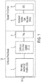
- FIG. 1 shows a block diagram of a receiver front-end (RFE) 100, according to some embodiments.
- RFE 100 includes an attenuating variable-gain amplifier (VGA) 1 that receives an RF input and provides its output to CTLE 4.
- VGA 1 and CTLE 4 are both in the continuous-time domain.
- the output of CTLE 4 may be provided to track-and-holds (T/Hs) 6 which sample the output of the CTLE 4 in a time-interleaved manner.
- T/Hs track-and-holds
- the output of T/Hs 6, each of which is at a fraction of full rate may be provided to the input of interleaved VGAs 8 in the discrete-time domain.
- the interleaved VGAs 8 may perform amplification and provide an output to an analog-to-digital converter (ADC) 10 to convert the received signals into the digital domain.
- ADC analog-to-digital converter
- RFE 100 may be configured to receive data transmitted at a rate of more than 10Gb/s, more than 20Gb/s, more than 30Gb/s, more than 40Gb/s, more than 50Gb/s, or more than any other suitable value. In some embodiments, RFE 100 may be configured to receive data transmitted at a rate between 40Gb/s and 80Gb/s, or within any range within such range. However, the techniques and apparatus described herein are not limited to a particular data rate.
- VGA 1 may provide only attenuation or unity gain, and no amplification, such that the gain of VGA 1 is less than one.
- the attenuation of VGA 1 may be controllable to adjust for different signal conditions. By providing only attenuation in VGA 1, VGA 1 may have relatively low power consumption.
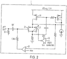
- FIG. 2 shows that VGA 1 may be implemented in a flipped source-follower configuration with a programmable NMOS load. Such a configuration can achieve wide bandwidth, good power efficiency, good fan-out and linearity.
- NMOS load transistors 21 may be realized by a plurality of NMOS transistors connected in parallel to provide very fine steps of impedance adjustment to adjust the gain of VGA 1.
- NMOS transistors 21 may be driven by inverters 22 based on a plurality of input control bits that set the degree of attenuation performed by NMOS load transistors 21.
- the VGA 1 may also include a source-follower transistor 23 having its gate coupled to the input of the VGA 1, its drain coupled to ground through a resistor, and its source serving as the output terminal.
- VGA 1 may also include current mirror transistors 24 and 25.
- VGA 1 may also include a feedback path extending from the source of transistor 23 to a comparator 26 that maintains a common-mode voltage bias (Vcm) at the gate of transistor 23.
- Vcm common-mode voltage bias
- FIG. 3 shows an example of CTLE 4, according to some embodiments.
- the CTLE 4 may include a G m stage 11 and a transimpedance amplifier (TIA) 12.
- TIA 12 may be implemented by a regulated common-gate circuit configuration, as illustrated in FIG. 3 .
- the input of the TIA 12 may be connected to the output of the G m stage 11 at the connection point between transistors 41 and 42.
- a first transistor 42 may have its source connected to ground and its drain connected to the input of the TIA 12.
- the drain of transistor 42 may be biased at a bias voltage Vb.
- a second transistor 41 has its source connected to the input of the TIA 12 and its drain connected to a resistor R L .
- Resistor R L has a first terminal connected to the drain of transistor 41 and a second terminal connected to an inductor L sp.
- Inductor L sp has a first terminal connected to resistor 43 and a second terminal connected to V DD .
- Inductor L sp may improve bandwidth, but is optional.
- inductor L sp may be omitted and the second terminal of the resistor 43 may be connected to V DD .
- Regulation is provided by amplifying the input provided to the TIA 12 by amplifier 44 and feeding back the amplified input signal to the gate of transistor 41.
- the regulated common-gate circuit configuration of FIG. 3 is an example, and that CTLE 4 may be implemented by other suitable circuit configurations.
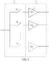
- FIG. 4 illustrates T/Hs 6 and VGAs 8.
- T/Hs 6 sample the incoming signal from the CTLE in an interleaved manner. For example, T/Hi may take a first sample, then T/H2, may take a sample at an appropriate phase delay, and so on until T/H n takes a sample.
- the phase delays between samples by respective T/Hs may be the clock period divided by the number of T/Hs. Any number n of T/Hs may be included, where n is a positive integer greater than or equal to two.
- the number of VGAs 8 may be equal to the number of T/Hs. Each T/H may provide a sample to its respective VGA 8.
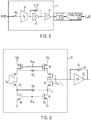
- FIG. 5 shows an example of a VGA 2 having an amplification block 81, a TIA 82, an output stage 83 and a feedback resistor 84.
- the amplification block 81 may be a G m stage that converts an incoming voltage into a current.
- VGA 2 is implemented using feedback.
- the TIA 82 may convert the current from the amplification block 81 back into a current. By performing interleaving and reducing the rate of the incoming signal, such feedback techniques can reduce power consumption while providing suitable performance.
- FIG. 6 shows an example of the amplification block 81 having an inverter-based configuration.
- the gain of the VGA may be controlled by controlling R D .
- Both NMOS and PMOS transistors contribute to the gain of the inverter-based Gm stage.
- the use of a PMOS/NMOS trans-conductance combination allows reusing the supply current, which improves energy efficiency.
- Such a configuration as shown in FIG. 6 can have double the Gm for the same current as compared to other Gm stage configurations.
- Such a configuration may allow for a smaller value of R L as compared to other Gm stage configurations, which results in lower noise and better bandwidth.
- R L the gain of the VGA
- amplification block configurations may be used.
- FIG. 7 shows a more detailed example of the RFE 100, according to some embodiments.
- an optional fixed attenuator may precede the VGA 1 and/or the CTLE 4.
- the CTLE may follow the VGA 1, as shown in FIGS. 1 and 8. However, in some embodiments, the locations of the VGA 1 and CTLE 4 may be reversed, and the CTLE 4 may precede the VGA 1.
- One or more signal buffers BUF0, BUF1, etc. may follow the VGA 1 and/or CTLE.
- the voltage source symbols following the T/Hs represent optional random offset-mismatch calibration hardware.
- Coupled or “connected” is meant to refer to circuit elements, or signals, that are either directly linked to one another or through intermediate components.
Landscapes
- Engineering & Computer Science (AREA)
- Computer Networks & Wireless Communication (AREA)
- Signal Processing (AREA)
- Power Engineering (AREA)
- Amplifiers (AREA)
Abstract
Description
- Receivers are used in electronics to receive signals transmitted through various transmission media, such as transmission lines, for example. Some types of receivers include analog-to-digital converters to convert the received signal into the digital domain. Receivers may include an analog front-end to condition the received analog signal prior to analog-to-digital conversion.
- Embodiments relate to a receiver front-end, comprising: a first variable-gain amplifier that performs attenuation; a continuous time linear equalizer coupled to an input or output of the first variable-gain amplifier, wherein a combination of the first variable-gain amplifier and the continuous time linear equalizer produces a processed signal; a plurality of track-and-hold circuits that sample the processed signal in an interleaved manner; and a plurality of second variable-gain amplifiers receiving input signals from the plurality of track-and-hold circuits respectively.
- The first variable-gain amplifier may not perform amplification.
- The first variable-gain amplifier may have a flipped source-follower configuration.
- The first variable-gain amplifier may have a programmable NMOS load to control a degree of the attenuation.
- The programmable NMOS load may be controlled by a plurality of inverters.
- The programmable NMOS load may be in parallel with a source-follower transistor of the first variable-gain amplifier.
- The receiver front-end may further comprise a feedback path from a source of the source-follower transistor to a gate of the source-follower transistor to regulate a voltage at the gate of the source-follower transistor.
- The continuous time linear equalizer may comprise a common-gate amplifier.
- The common-gate amplifier may comprise a first transistor having a first source connected to an input of the common-gate amplifier and a first drain, and a feedback path from the input of the common-gate amplifier to a gate of the first transistor.
- The feedback path may comprise an amplifier.
- The common-gate amplifier may further comprise a second transistor having a second drain connected to the input of the common-gate amplifier and a second source connected to a ground terminal.
- The common-gate amplifier may further comprise a resistor and an inductor between the first drain and a power terminal.
- A quantity of the plurality of track-and-hold circuits may be greater than or equal to two and a quantity of the plurality of second variable-gain amplifiers may be equal to the quantity of the plurality of track-and-hold circuits.
- An output of the first variable-gain amplifier may be coupled to an input of the continuous time linear equalizer.
- An input of the first variable-gain amplifier may be coupled to an output of the continuous time linear equalizer.
- A fixed attenuator may be coupled to an input of the first variable-gain amplifier or an input of the continuous time linear equalizer.
- The receiver front-end may further comprise at least one buffer that buffers the processed signal.
- This summary is provided by way of illustration and is not intended to be limiting.
- The accompanying drawings are not intended to be drawn to scale. In the drawings, each identical or nearly identical component that is illustrated in various figures is represented by a like numeral. For purposes of clarity, not every component may be labeled in every drawing. In the drawings:
-
FIG. 1 shows a block diagram of a receiver front-end (RFE), according to some embodiments. -
FIG. 2 shows an example of a circuit implementation of an attenuating VGA, according to some embodiments. -
FIG. 3 shows an example of a continuous-time linear equalizer (CTLE) having a transimpedance amplifier (TIA) with a regulated common-gate circuit configuration, according to some embodiments. -
FIG. 4 illustrates the T/Hs and VGAs of the RFE, according to some embodiments. -
FIG. 5 shows an example of an amplifying VGA having an amplification block, a TIA, an output stage and a feedback resistor, according to some embodiments. -
FIG. 6 shows an example of theamplification block 82 having an inverter-based configuration, according to some embodiments. -
FIG. 7 shows a more detailed example of the RFE ofFIG. 1 , according to some embodiments. - The inventors have recognized a number of disadvantages with existing analog front-ends for analog-to-digital converter (ADC) based receivers. A number of such analog front-ends are power inefficient, have significant variations in performance due to process, voltage and temperature variations, large area consumption, significant noise degradation, include the need for a high-voltage supply, have limited voltage headroom and have limited linearity, for example. With such analog front-ends, there may be a need to cascade a significant number of stages to achieve the target gain and peaking, which may reduce linearity.
- In some embodiments, a receiver front-end includes a continuous time linear equalizer (CTLE) and a variable gain amplifier (VGA). A CTLE can partially reverse the low-pass filter effects of limited channel bandwidth. The CTLE may be a high-pass filter. A CTLE may be realized in the continuous-time domain. The use of a VGA can assist with the need to cover many different reception channels with different frequency characteristics. The gain needed can vary from large values when performing amplification to small values when performing attenuation. The gain step may need to be very small (<0.2 dB). VGAs as described herein can provide suitable characteristics. The inventors have recognized and appreciated that VGA attenuation can be implemented at full-rate without significant disadvantages, but providing gain in a VGA can be disadvantageous at full-rate. The inventors have recognized and appreciated that a discrete-time implementation of an amplifying VGA combined with interleaving allows for lower-rate implementations.
- In some embodiments, a receiver front-end includes a first VGA in the continuous-time domain that only performs attenuation (it does not perform amplification). The receiver front-end may also include a CTLE in the continuous-time domain. The receiver front-end also may include a plurality of interleaved VGAs in the discrete-time domain configured to perform amplification. By using interleaving and moving the amplifying VGAs to the discrete-time domain at a lower rate, a number of advantages may be realized. Lower bandwidth requirements can enable feedback-based amplifying VGAs to be used, which may improve linearity and stability to process, voltage and temperature variations. The linearity specifications of the CTLE and track-and-hold (T/H) circuits may be reduced by limiting their output swing. At a reduced sampling rate the amplifying VGA is more power efficient and can achieve a larger gain at a lower bit-rate than at full bit-rate. At a reduced sampling rate the amplifying VGA may have no need for inductors, which leads to a large area savings and better pulse response (i.e., reduced ringing).
-
FIG. 1 shows a block diagram of a receiver front-end (RFE) 100, according to some embodiments. RFE 100 includes an attenuating variable-gain amplifier (VGA) 1 that receives an RF input and provides its output toCTLE 4.VGA 1 andCTLE 4 are both in the continuous-time domain. The output ofCTLE 4 may be provided to track-and-holds (T/Hs) 6 which sample the output of theCTLE 4 in a time-interleaved manner. The output of T/Hs 6, each of which is at a fraction of full rate, may be provided to the input of interleavedVGAs 8 in the discrete-time domain. Theinterleaved VGAs 8 may perform amplification and provide an output to an analog-to-digital converter (ADC) 10 to convert the received signals into the digital domain. - In some embodiments, RFE 100 may be configured to receive data transmitted at a rate of more than 10Gb/s, more than 20Gb/s, more than 30Gb/s, more than 40Gb/s, more than 50Gb/s, or more than any other suitable value. In some embodiments, RFE 100 may be configured to receive data transmitted at a rate between 40Gb/s and 80Gb/s, or within any range within such range. However, the techniques and apparatus described herein are not limited to a particular data rate.
- In some embodiments,
VGA 1 may provide only attenuation or unity gain, and no amplification, such that the gain ofVGA 1 is less than one. The attenuation ofVGA 1 may be controllable to adjust for different signal conditions. By providing only attenuation inVGA 1,VGA 1 may have relatively low power consumption. - One example of a circuit implementation of
VGA 1 is illustrated inFIG. 2. FIG. 2 shows thatVGA 1 may be implemented in a flipped source-follower configuration with a programmable NMOS load. Such a configuration can achieve wide bandwidth, good power efficiency, good fan-out and linearity.NMOS load transistors 21 may be realized by a plurality of NMOS transistors connected in parallel to provide very fine steps of impedance adjustment to adjust the gain ofVGA 1.NMOS transistors 21 may be driven byinverters 22 based on a plurality of input control bits that set the degree of attenuation performed byNMOS load transistors 21. TheVGA 1 may also include a source-follower transistor 23 having its gate coupled to the input of theVGA 1, its drain coupled to ground through a resistor, and its source serving as the output terminal.VGA 1 may also includecurrent mirror transistors VGA 1 may also include a feedback path extending from the source oftransistor 23 to acomparator 26 that maintains a common-mode voltage bias (Vcm) at the gate oftransistor 23. However, it should be appreciated that the flipped source-follower configuration ofFIG. 2 is an example, and thatVGA 1 may be implemented by other suitable circuit configurations. -
FIG. 3 shows an example ofCTLE 4, according to some embodiments. TheCTLE 4 may include a Gm stage 11 and a transimpedance amplifier (TIA) 12. In some embodiments,TIA 12 may be implemented by a regulated common-gate circuit configuration, as illustrated inFIG. 3 . The input of theTIA 12 may be connected to the output of the Gm stage 11 at the connection point betweentransistors 41 and 42. Afirst transistor 42 may have its source connected to ground and its drain connected to the input of theTIA 12. The drain oftransistor 42 may be biased at a bias voltage Vb. A second transistor 41 has its source connected to the input of theTIA 12 and its drain connected to a resistor RL. Resistor RL has a first terminal connected to the drain of transistor 41 and a second terminal connected to an inductor Lsp. Inductor Lsp has a first terminal connected toresistor 43 and a second terminal connected to VDD. Inductor Lsp may improve bandwidth, but is optional. In some embodiments, inductor Lsp may be omitted and the second terminal of theresistor 43 may be connected to VDD. Regulation is provided by amplifying the input provided to theTIA 12 byamplifier 44 and feeding back the amplified input signal to the gate of transistor 41. However, it should be appreciated that the regulated common-gate circuit configuration ofFIG. 3 is an example, and thatCTLE 4 may be implemented by other suitable circuit configurations. -
FIG. 4 illustrates T/Hs 6 andVGAs 8. T/Hs 6 sample the incoming signal from the CTLE in an interleaved manner. For example, T/Hi may take a first sample, then T/H2, may take a sample at an appropriate phase delay, and so on until T/Hn takes a sample. The phase delays between samples by respective T/Hs may be the clock period divided by the number of T/Hs. Any number n of T/Hs may be included, where n is a positive integer greater than or equal to two. The number ofVGAs 8 may be equal to the number of T/Hs. Each T/H may provide a sample to itsrespective VGA 8. -
FIG. 5 shows an example of a VGA 2 having anamplification block 81, aTIA 82, anoutput stage 83 and afeedback resistor 84. Theamplification block 81 may be a Gm stage that converts an incoming voltage into a current. In some embodiments, VGA 2 is implemented using feedback. TheTIA 82 may convert the current from theamplification block 81 back into a current. By performing interleaving and reducing the rate of the incoming signal, such feedback techniques can reduce power consumption while providing suitable performance. -
FIG. 6 shows an example of theamplification block 81 having an inverter-based configuration. In some embodiments, the gain of the VGA may be controlled by controlling RD. Both NMOS and PMOS transistors contribute to the gain of the inverter-based Gm stage. The use of a PMOS/NMOS trans-conductance combination allows reusing the supply current, which improves energy efficiency. Such a configuration as shown inFIG. 6 can have double the Gm for the same current as compared to other Gm stage configurations. Such a configuration may allow for a smaller value of RL as compared to other Gm stage configurations, which results in lower noise and better bandwidth. However, it should be appreciated that this is an example, and any of a variety of VGA configurations and amplification block configurations may be used. -
FIG. 7 shows a more detailed example of theRFE 100, according to some embodiments. As illustrated, an optional fixed attenuator may precede theVGA 1 and/or theCTLE 4. The CTLE may follow theVGA 1, as shown inFIGS. 1 and 8. However, in some embodiments, the locations of theVGA 1 andCTLE 4 may be reversed, and theCTLE 4 may precede theVGA 1. One or more signal buffers BUF0, BUF1, etc., may follow theVGA 1 and/or CTLE. The voltage source symbols following the T/Hs represent optional random offset-mismatch calibration hardware. In this example, there are eight T/Hs 6 and eightVGAs 8, which can reduce the rate of the signals processed by theVGAs 8 by a factor of eight. For example, instead of having asingle VGA 8 sampling at full-rate (e.g., 112 Gbps), each of the eightVGAs 8 may sample at a rate of 14 Gbps, which reduces the requirements of theVGAs 8. - Various aspects of the apparatus and techniques described herein may be used alone, in combination, or in a variety of arrangements not specifically discussed in the embodiments described in the foregoing description and is therefore not limited in its application to the details and arrangement of components set forth in the foregoing description or illustrated in the drawings. For example, aspects described in one embodiment may be combined in any manner with aspects described in other embodiments.
- Use of ordinal terms such as "first", "second", "third", etc., in the claims to modify a claim element does not by itself connote any priority, precedence, or order of one claim element over another or the temporal order in which acts of a method are performed, but are used merely as labels to distinguish one claim element having a certain name from another element having a same name (but for use of the ordinal term) to distinguish the claim elements.
- Also, the phraseology and terminology used herein is for the purpose of description and should not be regarded as limiting. The use of "including", "comprising", "having", "containing" or "involving" and variations thereof herein, is meant to encompass the items listed thereafter and equivalents thereof as well as additional items.
- The use of "coupled" or "connected" is meant to refer to circuit elements, or signals, that are either directly linked to one another or through intermediate components.
Claims (15)
- A receiver front-end, comprising:a first variable-gain amplifier that performs attenuation;a continuous time linear equalizer coupled to an input or output of the first variable-gain amplifier, wherein a combination of the first variable-gain amplifier and the continuous time linear equalizer produces a processed signal;a plurality of track-and-hold circuits that sample the processed signal in an interleaved manner; anda plurality of second variable-gain amplifiers receiving input signals from the plurality of track-and-hold circuits respectively.
- The receiver front-end of claim 1, wherein the first variable-gain amplifier does not perform amplification.
- The receiver front-end of any preceding claim, wherein the first variable-gain amplifier has a flipped source-follower configuration.
- The receiver front-end of any preceding claim, wherein the first variable-gain amplifier has a programmable NMOS load to control a degree of the attenuation.
- The receiver front-end of claim 4, wherein the programmable NMOS load is controlled by a plurality of inverters.
- The receiver front-end of claim 4 or claim 5, wherein the programmable NMOS load is in parallel with a source-follower transistor of the first variable-gain amplifier.
- The receiver front-end of claim 6, further comprising a feedback path from a source of the source-follower transistor to a gate of the source-follower transistor to regulate a voltage at the gate of the source-follower transistor.
- The receiver front-end of any preceding claim, wherein the continuous time linear equalizer comprises a common-gate amplifier.
- The receiver front-end of claim 8, wherein the common-gate amplifier comprises a first transistor having a first source connected to an input of the common-gate amplifier and a first drain, and a feedback path from the input of the common-gate amplifier to a gate of the first transistor.
- The receiver front-end of claim 9, wherein the feedback path comprises an amplifier.
- The receiver front-end of claim 9 or claim 10, wherein the common-gate amplifier further comprises a second transistor having a second drain connected to the input of the common-gate amplifier and a second source connected to a ground terminal.
- The receiver front-end of claim 11, wherein the common-gate amplifier further comprises a resistor and an inductor between the first drain and a power terminal.
- The receiver front-end of any preceding claim, wherein a quantity of the plurality of track-and-hold circuits is greater than or equal to two and a quantity of the plurality of second variable-gain amplifiers is equal to the quantity of the plurality of track-and-hold circuits.
- The receiver front-end of any preceding claim, wherein an output of the first variable-gain amplifier is coupled to an input of the continuous time linear equalizer.
- The receiver front-end of any preceding claim, wherein an input of the first variable-gain amplifier is coupled to an output of the continuous time linear equalizer.
Applications Claiming Priority (2)
| Application Number | Priority Date | Filing Date | Title |
|---|---|---|---|
| US201962859770P | 2019-06-11 | 2019-06-11 | |
| US16/872,099 US11469729B2 (en) | 2019-06-11 | 2020-05-11 | Hybrid receiver front-end |
Publications (2)
| Publication Number | Publication Date |
|---|---|
| EP3751807A1 true EP3751807A1 (en) | 2020-12-16 |
| EP3751807B1 EP3751807B1 (en) | 2024-02-28 |
Family
ID=71092322
Family Applications (1)
| Application Number | Title | Priority Date | Filing Date |
|---|---|---|---|
| EP20179368.4A Active EP3751807B1 (en) | 2019-06-11 | 2020-06-10 | Hybrid receiver front-end |
Country Status (4)
| Country | Link |
|---|---|
| US (1) | US11469729B2 (en) |
| EP (1) | EP3751807B1 (en) |
| CN (1) | CN112073077B (en) |
| TW (1) | TWI745970B (en) |
Cited By (1)
| Publication number | Priority date | Publication date | Assignee | Title |
|---|---|---|---|---|
| CN121547013A (en) * | 2026-01-21 | 2026-02-17 | 安徽大学未来产业创新研究院 | A continuous-time linear equalizer circuit based on attenuator structure |
Families Citing this family (4)
| Publication number | Priority date | Publication date | Assignee | Title |
|---|---|---|---|---|
| CN114448353B (en) * | 2022-01-21 | 2025-08-19 | 中国科学技术大学 | Analog equalizer |
| US11601309B1 (en) | 2022-02-14 | 2023-03-07 | 1-Via Ltd | Multi-stage continuous time linear equalizer with reconfigurable inductor scheme |
| CN115051896B (en) * | 2022-08-15 | 2022-11-08 | 高澈科技(上海)有限公司 | Ultra-high-speed serial port receiver and continuous time linear equalizer thereof |
| US20260058849A1 (en) * | 2024-08-22 | 2026-02-26 | Qualcomm Incorporated | Continuous time linear equalizer employing current-reuse and current-stealing architecture |
Family Cites Families (12)
| Publication number | Priority date | Publication date | Assignee | Title |
|---|---|---|---|---|
| US8792521B2 (en) | 2011-09-23 | 2014-07-29 | Broadcom Corporation | Multi-standard front end using wideband data converters |
| US8964825B2 (en) * | 2012-02-17 | 2015-02-24 | International Business Machines Corporation | Analog signal current integrators with tunable peaking function |
| WO2015130257A1 (en) | 2014-02-25 | 2015-09-03 | Intel Corporation | Apparatus, system and method of simultaneous transmit and receive (str) wireless communication |
| US9385695B2 (en) * | 2014-06-06 | 2016-07-05 | Qualcomm Incorporated | Offset calibration for low power and high performance receiver |
| US9397623B1 (en) | 2015-02-27 | 2016-07-19 | Huawei Technologies Co., Ltd. | Dual path double zero continuous time linear equalizer |
| US9602116B1 (en) * | 2016-01-07 | 2017-03-21 | Inphi Corporation | Interleaved successive approximation register analog to digital converter |
| US9654310B1 (en) | 2016-11-19 | 2017-05-16 | Nxp Usa, Inc. | Analog delay cell and tapped delay line comprising the analog delay cell |
| US10270409B1 (en) | 2017-05-16 | 2019-04-23 | Inphi Corporation | Variable gain amplifiers for communication systems |
| US10243570B1 (en) * | 2017-07-28 | 2019-03-26 | Inphi Corporation | Charge pump circuits for clock and data recovery |
| US10608848B1 (en) * | 2018-10-04 | 2020-03-31 | Macom Technology Solutions Holdings, Inc. | CTLE adaptation based on post-cursors |
| CN109450471A (en) | 2018-10-15 | 2019-03-08 | 上海兆芯集成电路有限公司 | Acceptor circuit and the method for increasing bandwidth |
| US10396811B1 (en) * | 2019-01-15 | 2019-08-27 | Globalfoundries Inc. | Temperature compensation for reference voltages in an analog-to-digital converter |
-
2020
- 2020-05-11 US US16/872,099 patent/US11469729B2/en active Active
- 2020-05-21 CN CN202010435444.3A patent/CN112073077B/en active Active
- 2020-05-21 TW TW109116846A patent/TWI745970B/en active
- 2020-06-10 EP EP20179368.4A patent/EP3751807B1/en active Active
Non-Patent Citations (4)
| Title |
|---|
| ALI TAMER ET AL: "6.4 A 180mW 56Gb/s DSP-Based Transceiver for High Density IOs in Data Center Switches in 7nm FinFET Technology", 2019 IEEE INTERNATIONAL SOLID- STATE CIRCUITS CONFERENCE - (ISSCC), IEEE, 17 February 2019 (2019-02-17), pages 118 - 120, XP033528000, DOI: 10.1109/ISSCC.2019.8662523 * |
| DUVVURI DIVYA ET AL: "Design and analysis of a current mode integrated CTLE with charge mode adaptation", MICROELECTRONICS JOURNAL, MACKINTOSH PUBLICATIONS LTD. LUTON, GB, vol. 53, 30 April 2016 (2016-04-30), pages 81 - 89, XP029579162, ISSN: 0026-2692, DOI: 10.1016/J.MEJO.2016.04.013 * |
| E-HUNG CHEN ET AL: "Power Optimized ADC-Based Serial Link Receiver", IEEE JOURNAL OF SOLID-STATE CIRCUITS, IEEE, USA, vol. 47, no. 4, 1 April 2012 (2012-04-01), pages 938 - 951, XP011440037, ISSN: 0018-9200, DOI: 10.1109/JSSC.2012.2185356 * |
| JUN CAO ET AL: "A 500 mW ADC-Based CMOS AFE With Digital Calibration for 10 Gb/s Serial Links Over KR-Backplane and Multimode Fiber", IEEE JOURNAL OF SOLID-STATE CIRCUITS, IEEE, USA, vol. 45, no. 6, 1 June 2010 (2010-06-01), pages 1172 - 1185, XP011311101, ISSN: 0018-9200, DOI: 10.1109/JSSC.2010.2047473 * |
Cited By (1)
| Publication number | Priority date | Publication date | Assignee | Title |
|---|---|---|---|---|
| CN121547013A (en) * | 2026-01-21 | 2026-02-17 | 安徽大学未来产业创新研究院 | A continuous-time linear equalizer circuit based on attenuator structure |
Also Published As
| Publication number | Publication date |
|---|---|
| CN112073077A (en) | 2020-12-11 |
| TWI745970B (en) | 2021-11-11 |
| US20200395909A1 (en) | 2020-12-17 |
| CN112073077B (en) | 2022-03-15 |
| TW202101919A (en) | 2021-01-01 |
| US11469729B2 (en) | 2022-10-11 |
| EP3751807B1 (en) | 2024-02-28 |
Similar Documents
| Publication | Publication Date | Title |
|---|---|---|
| US11469729B2 (en) | Hybrid receiver front-end | |
| US9288085B2 (en) | Continuous-time linear equalizer for high-speed receiving unit | |
| US10313165B2 (en) | Finite impulse response analog receive filter with amplifier-based delay chain | |
| US9099976B2 (en) | Methods for digitally-controlled automatic gain amplification | |
| TWI777796B (en) | Low power receiver with equalization circuit and method therefor | |
| CN105871344B (en) | The apparatus and system of rail-to-rail amplifier | |
| JP2019507552A (en) | Auto gain control circuit interleaved with linear gain sign | |
| CN116016060B (en) | Receiver analog front-end multistage equalizer for high-speed serial link | |
| CN109450471A (en) | Acceptor circuit and the method for increasing bandwidth | |
| US7969218B2 (en) | Receiver for reducing intersymbol interference of a channel and compensating for signal gain loss, and method thereof | |
| US20080218257A1 (en) | Distributed track-and-hold amplifier | |
| US10715359B1 (en) | Decision feedback equalizer | |
| US20090027128A1 (en) | Variable gain amplifier | |
| US20030218502A1 (en) | Variable gain amplifier | |
| US9385893B2 (en) | Modular low power serializer-deserializer | |
| CN110995186A (en) | Variable gain amplifier circuit | |
| US7236017B2 (en) | High speed sample-and-hold circuit | |
| KR100842775B1 (en) | Two-stage equalizer, two-stage equalization method, receiver and communication system for high speed communication | |
| US12132492B2 (en) | Method and system for improving analog-to-digital conversion performance | |
| Hadji-Abdolhamid et al. | A 400-MHz 6-bit ADC with a partial analog equalizer for coaxial cable channels | |
| JP6781105B2 (en) | Track and hold circuit | |
| US10574491B2 (en) | Signal distribution circuit and signal distribution circuit system | |
| US11706060B2 (en) | Serial-link receiver using time-interleaved discrete time gain | |
| US20260058849A1 (en) | Continuous time linear equalizer employing current-reuse and current-stealing architecture | |
| KR20250106070A (en) | Sample and hold circuit and analog-digital converter circuit including the same |
Legal Events
| Date | Code | Title | Description |
|---|---|---|---|
| PUAI | Public reference made under article 153(3) epc to a published international application that has entered the european phase |
Free format text: ORIGINAL CODE: 0009012 |
|
| STAA | Information on the status of an ep patent application or granted ep patent |
Free format text: STATUS: THE APPLICATION HAS BEEN PUBLISHED |
|
| AK | Designated contracting states |
Kind code of ref document: A1 Designated state(s): AL AT BE BG CH CY CZ DE DK EE ES FI FR GB GR HR HU IE IS IT LI LT LU LV MC MK MT NL NO PL PT RO RS SE SI SK SM TR |
|
| AX | Request for extension of the european patent |
Extension state: BA ME |
|
| STAA | Information on the status of an ep patent application or granted ep patent |
Free format text: STATUS: REQUEST FOR EXAMINATION WAS MADE |
|
| 17P | Request for examination filed |
Effective date: 20210611 |
|
| RBV | Designated contracting states (corrected) |
Designated state(s): AL AT BE BG CH CY CZ DE DK EE ES FI FR GB GR HR HU IE IS IT LI LT LU LV MC MK MT NL NO PL PT RO RS SE SI SK SM TR |
|
| STAA | Information on the status of an ep patent application or granted ep patent |
Free format text: STATUS: EXAMINATION IS IN PROGRESS |
|
| 17Q | First examination report despatched |
Effective date: 20221010 |
|
| P01 | Opt-out of the competence of the unified patent court (upc) registered |
Effective date: 20230627 |
|
| GRAP | Despatch of communication of intention to grant a patent |
Free format text: ORIGINAL CODE: EPIDOSNIGR1 |
|
| STAA | Information on the status of an ep patent application or granted ep patent |
Free format text: STATUS: GRANT OF PATENT IS INTENDED |
|
| INTG | Intention to grant announced |
Effective date: 20231121 |
|
| GRAS | Grant fee paid |
Free format text: ORIGINAL CODE: EPIDOSNIGR3 |
|
| GRAA | (expected) grant |
Free format text: ORIGINAL CODE: 0009210 |
|
| STAA | Information on the status of an ep patent application or granted ep patent |
Free format text: STATUS: THE PATENT HAS BEEN GRANTED |
|
| AK | Designated contracting states |
Kind code of ref document: B1 Designated state(s): AL AT BE BG CH CY CZ DE DK EE ES FI FR GB GR HR HU IE IS IT LI LT LU LV MC MK MT NL NO PL PT RO RS SE SI SK SM TR |
|
| REG | Reference to a national code |
Ref country code: GB Ref legal event code: FG4D |
|
| REG | Reference to a national code |
Ref country code: CH Ref legal event code: EP |
|
| REG | Reference to a national code |
Ref country code: DE Ref legal event code: R096 Ref document number: 602020026296 Country of ref document: DE |
|
| REG | Reference to a national code |
Ref country code: IE Ref legal event code: FG4D |
|
| REG | Reference to a national code |
Ref country code: LT Ref legal event code: MG9D |
|
| PG25 | Lapsed in a contracting state [announced via postgrant information from national office to epo] |
Ref country code: IS Free format text: LAPSE BECAUSE OF FAILURE TO SUBMIT A TRANSLATION OF THE DESCRIPTION OR TO PAY THE FEE WITHIN THE PRESCRIBED TIME-LIMIT Effective date: 20240628 |
|
| REG | Reference to a national code |
Ref country code: NL Ref legal event code: MP Effective date: 20240228 |
|
| PG25 | Lapsed in a contracting state [announced via postgrant information from national office to epo] |
Ref country code: LT Free format text: LAPSE BECAUSE OF FAILURE TO SUBMIT A TRANSLATION OF THE DESCRIPTION OR TO PAY THE FEE WITHIN THE PRESCRIBED TIME-LIMIT Effective date: 20240228 |
|
| PG25 | Lapsed in a contracting state [announced via postgrant information from national office to epo] |
Ref country code: GR Free format text: LAPSE BECAUSE OF FAILURE TO SUBMIT A TRANSLATION OF THE DESCRIPTION OR TO PAY THE FEE WITHIN THE PRESCRIBED TIME-LIMIT Effective date: 20240529 |
|
| PG25 | Lapsed in a contracting state [announced via postgrant information from national office to epo] |
Ref country code: HR Free format text: LAPSE BECAUSE OF FAILURE TO SUBMIT A TRANSLATION OF THE DESCRIPTION OR TO PAY THE FEE WITHIN THE PRESCRIBED TIME-LIMIT Effective date: 20240228 Ref country code: RS Free format text: LAPSE BECAUSE OF FAILURE TO SUBMIT A TRANSLATION OF THE DESCRIPTION OR TO PAY THE FEE WITHIN THE PRESCRIBED TIME-LIMIT Effective date: 20240528 Ref country code: NL Free format text: LAPSE BECAUSE OF FAILURE TO SUBMIT A TRANSLATION OF THE DESCRIPTION OR TO PAY THE FEE WITHIN THE PRESCRIBED TIME-LIMIT Effective date: 20240228 |
|
| PG25 | Lapsed in a contracting state [announced via postgrant information from national office to epo] |
Ref country code: ES Free format text: LAPSE BECAUSE OF FAILURE TO SUBMIT A TRANSLATION OF THE DESCRIPTION OR TO PAY THE FEE WITHIN THE PRESCRIBED TIME-LIMIT Effective date: 20240228 |
|
| PG25 | Lapsed in a contracting state [announced via postgrant information from national office to epo] |
Ref country code: RS Free format text: LAPSE BECAUSE OF FAILURE TO SUBMIT A TRANSLATION OF THE DESCRIPTION OR TO PAY THE FEE WITHIN THE PRESCRIBED TIME-LIMIT Effective date: 20240528 Ref country code: NO Free format text: LAPSE BECAUSE OF FAILURE TO SUBMIT A TRANSLATION OF THE DESCRIPTION OR TO PAY THE FEE WITHIN THE PRESCRIBED TIME-LIMIT Effective date: 20240528 Ref country code: NL Free format text: LAPSE BECAUSE OF FAILURE TO SUBMIT A TRANSLATION OF THE DESCRIPTION OR TO PAY THE FEE WITHIN THE PRESCRIBED TIME-LIMIT Effective date: 20240228 Ref country code: LT Free format text: LAPSE BECAUSE OF FAILURE TO SUBMIT A TRANSLATION OF THE DESCRIPTION OR TO PAY THE FEE WITHIN THE PRESCRIBED TIME-LIMIT Effective date: 20240228 Ref country code: IS Free format text: LAPSE BECAUSE OF FAILURE TO SUBMIT A TRANSLATION OF THE DESCRIPTION OR TO PAY THE FEE WITHIN THE PRESCRIBED TIME-LIMIT Effective date: 20240628 Ref country code: HR Free format text: LAPSE BECAUSE OF FAILURE TO SUBMIT A TRANSLATION OF THE DESCRIPTION OR TO PAY THE FEE WITHIN THE PRESCRIBED TIME-LIMIT Effective date: 20240228 Ref country code: GR Free format text: LAPSE BECAUSE OF FAILURE TO SUBMIT A TRANSLATION OF THE DESCRIPTION OR TO PAY THE FEE WITHIN THE PRESCRIBED TIME-LIMIT Effective date: 20240529 Ref country code: FI Free format text: LAPSE BECAUSE OF FAILURE TO SUBMIT A TRANSLATION OF THE DESCRIPTION OR TO PAY THE FEE WITHIN THE PRESCRIBED TIME-LIMIT Effective date: 20240228 Ref country code: ES Free format text: LAPSE BECAUSE OF FAILURE TO SUBMIT A TRANSLATION OF THE DESCRIPTION OR TO PAY THE FEE WITHIN THE PRESCRIBED TIME-LIMIT Effective date: 20240228 Ref country code: BG Free format text: LAPSE BECAUSE OF FAILURE TO SUBMIT A TRANSLATION OF THE DESCRIPTION OR TO PAY THE FEE WITHIN THE PRESCRIBED TIME-LIMIT Effective date: 20240228 |
|
| PG25 | Lapsed in a contracting state [announced via postgrant information from national office to epo] |
Ref country code: PT Free format text: LAPSE BECAUSE OF FAILURE TO SUBMIT A TRANSLATION OF THE DESCRIPTION OR TO PAY THE FEE WITHIN THE PRESCRIBED TIME-LIMIT Effective date: 20240628 Ref country code: PL Free format text: LAPSE BECAUSE OF FAILURE TO SUBMIT A TRANSLATION OF THE DESCRIPTION OR TO PAY THE FEE WITHIN THE PRESCRIBED TIME-LIMIT Effective date: 20240228 |
|
| REG | Reference to a national code |
Ref country code: AT Ref legal event code: MK05 Ref document number: 1662277 Country of ref document: AT Kind code of ref document: T Effective date: 20240228 |
|
| PG25 | Lapsed in a contracting state [announced via postgrant information from national office to epo] |
Ref country code: SE Free format text: LAPSE BECAUSE OF FAILURE TO SUBMIT A TRANSLATION OF THE DESCRIPTION OR TO PAY THE FEE WITHIN THE PRESCRIBED TIME-LIMIT Effective date: 20240228 Ref country code: PT Free format text: LAPSE BECAUSE OF FAILURE TO SUBMIT A TRANSLATION OF THE DESCRIPTION OR TO PAY THE FEE WITHIN THE PRESCRIBED TIME-LIMIT Effective date: 20240628 Ref country code: PL Free format text: LAPSE BECAUSE OF FAILURE TO SUBMIT A TRANSLATION OF THE DESCRIPTION OR TO PAY THE FEE WITHIN THE PRESCRIBED TIME-LIMIT Effective date: 20240228 Ref country code: LV Free format text: LAPSE BECAUSE OF FAILURE TO SUBMIT A TRANSLATION OF THE DESCRIPTION OR TO PAY THE FEE WITHIN THE PRESCRIBED TIME-LIMIT Effective date: 20240228 |
|
| PG25 | Lapsed in a contracting state [announced via postgrant information from national office to epo] |
Ref country code: DK Free format text: LAPSE BECAUSE OF FAILURE TO SUBMIT A TRANSLATION OF THE DESCRIPTION OR TO PAY THE FEE WITHIN THE PRESCRIBED TIME-LIMIT Effective date: 20240228 |
|
| PG25 | Lapsed in a contracting state [announced via postgrant information from national office to epo] |
Ref country code: SM Free format text: LAPSE BECAUSE OF FAILURE TO SUBMIT A TRANSLATION OF THE DESCRIPTION OR TO PAY THE FEE WITHIN THE PRESCRIBED TIME-LIMIT Effective date: 20240228 |
|
| PG25 | Lapsed in a contracting state [announced via postgrant information from national office to epo] |
Ref country code: EE Free format text: LAPSE BECAUSE OF FAILURE TO SUBMIT A TRANSLATION OF THE DESCRIPTION OR TO PAY THE FEE WITHIN THE PRESCRIBED TIME-LIMIT Effective date: 20240228 Ref country code: CZ Free format text: LAPSE BECAUSE OF FAILURE TO SUBMIT A TRANSLATION OF THE DESCRIPTION OR TO PAY THE FEE WITHIN THE PRESCRIBED TIME-LIMIT Effective date: 20240228 |
|
| PG25 | Lapsed in a contracting state [announced via postgrant information from national office to epo] |
Ref country code: AT Free format text: LAPSE BECAUSE OF FAILURE TO SUBMIT A TRANSLATION OF THE DESCRIPTION OR TO PAY THE FEE WITHIN THE PRESCRIBED TIME-LIMIT Effective date: 20240228 |
|
| PG25 | Lapsed in a contracting state [announced via postgrant information from national office to epo] |
Ref country code: SK Free format text: LAPSE BECAUSE OF FAILURE TO SUBMIT A TRANSLATION OF THE DESCRIPTION OR TO PAY THE FEE WITHIN THE PRESCRIBED TIME-LIMIT Effective date: 20240228 |
|
| PG25 | Lapsed in a contracting state [announced via postgrant information from national office to epo] |
Ref country code: SM Free format text: LAPSE BECAUSE OF FAILURE TO SUBMIT A TRANSLATION OF THE DESCRIPTION OR TO PAY THE FEE WITHIN THE PRESCRIBED TIME-LIMIT Effective date: 20240228 Ref country code: SK Free format text: LAPSE BECAUSE OF FAILURE TO SUBMIT A TRANSLATION OF THE DESCRIPTION OR TO PAY THE FEE WITHIN THE PRESCRIBED TIME-LIMIT Effective date: 20240228 Ref country code: RO Free format text: LAPSE BECAUSE OF FAILURE TO SUBMIT A TRANSLATION OF THE DESCRIPTION OR TO PAY THE FEE WITHIN THE PRESCRIBED TIME-LIMIT Effective date: 20240228 Ref country code: EE Free format text: LAPSE BECAUSE OF FAILURE TO SUBMIT A TRANSLATION OF THE DESCRIPTION OR TO PAY THE FEE WITHIN THE PRESCRIBED TIME-LIMIT Effective date: 20240228 Ref country code: DK Free format text: LAPSE BECAUSE OF FAILURE TO SUBMIT A TRANSLATION OF THE DESCRIPTION OR TO PAY THE FEE WITHIN THE PRESCRIBED TIME-LIMIT Effective date: 20240228 Ref country code: CZ Free format text: LAPSE BECAUSE OF FAILURE TO SUBMIT A TRANSLATION OF THE DESCRIPTION OR TO PAY THE FEE WITHIN THE PRESCRIBED TIME-LIMIT Effective date: 20240228 Ref country code: AT Free format text: LAPSE BECAUSE OF FAILURE TO SUBMIT A TRANSLATION OF THE DESCRIPTION OR TO PAY THE FEE WITHIN THE PRESCRIBED TIME-LIMIT Effective date: 20240228 |
|
| REG | Reference to a national code |
Ref country code: DE Ref legal event code: R097 Ref document number: 602020026296 Country of ref document: DE |
|
| PG25 | Lapsed in a contracting state [announced via postgrant information from national office to epo] |
Ref country code: IT Free format text: LAPSE BECAUSE OF FAILURE TO SUBMIT A TRANSLATION OF THE DESCRIPTION OR TO PAY THE FEE WITHIN THE PRESCRIBED TIME-LIMIT Effective date: 20240228 |
|
| PG25 | Lapsed in a contracting state [announced via postgrant information from national office to epo] |
Ref country code: IT Free format text: LAPSE BECAUSE OF FAILURE TO SUBMIT A TRANSLATION OF THE DESCRIPTION OR TO PAY THE FEE WITHIN THE PRESCRIBED TIME-LIMIT Effective date: 20240228 |
|
| PLBE | No opposition filed within time limit |
Free format text: ORIGINAL CODE: 0009261 |
|
| STAA | Information on the status of an ep patent application or granted ep patent |
Free format text: STATUS: NO OPPOSITION FILED WITHIN TIME LIMIT |
|
| PG25 | Lapsed in a contracting state [announced via postgrant information from national office to epo] |
Ref country code: MC Free format text: LAPSE BECAUSE OF FAILURE TO SUBMIT A TRANSLATION OF THE DESCRIPTION OR TO PAY THE FEE WITHIN THE PRESCRIBED TIME-LIMIT Effective date: 20240228 |
|
| REG | Reference to a national code |
Ref country code: CH Ref legal event code: PL |
|
| 26N | No opposition filed |
Effective date: 20241129 |
|
| PG25 | Lapsed in a contracting state [announced via postgrant information from national office to epo] |
Ref country code: LU Free format text: LAPSE BECAUSE OF NON-PAYMENT OF DUE FEES Effective date: 20240610 |
|
| PG25 | Lapsed in a contracting state [announced via postgrant information from national office to epo] |
Ref country code: IE Free format text: LAPSE BECAUSE OF NON-PAYMENT OF DUE FEES Effective date: 20240610 |
|
| PG25 | Lapsed in a contracting state [announced via postgrant information from national office to epo] |
Ref country code: BE Free format text: LAPSE BECAUSE OF NON-PAYMENT OF DUE FEES Effective date: 20240630 Ref country code: CH Free format text: LAPSE BECAUSE OF NON-PAYMENT OF DUE FEES Effective date: 20240630 Ref country code: SI Free format text: LAPSE BECAUSE OF FAILURE TO SUBMIT A TRANSLATION OF THE DESCRIPTION OR TO PAY THE FEE WITHIN THE PRESCRIBED TIME-LIMIT Effective date: 20240228 |
|
| REG | Reference to a national code |
Ref country code: BE Ref legal event code: MM Effective date: 20240630 |
|
| PGFP | Annual fee paid to national office [announced via postgrant information from national office to epo] |
Ref country code: DE Payment date: 20250429 Year of fee payment: 6 |
|
| PGFP | Annual fee paid to national office [announced via postgrant information from national office to epo] |
Ref country code: GB Payment date: 20250425 Year of fee payment: 6 |
|
| PGFP | Annual fee paid to national office [announced via postgrant information from national office to epo] |
Ref country code: FR Payment date: 20250508 Year of fee payment: 6 |
|
| PG25 | Lapsed in a contracting state [announced via postgrant information from national office to epo] |
Ref country code: CY Free format text: LAPSE BECAUSE OF FAILURE TO SUBMIT A TRANSLATION OF THE DESCRIPTION OR TO PAY THE FEE WITHIN THE PRESCRIBED TIME-LIMIT; INVALID AB INITIO Effective date: 20200610 |
|
| PG25 | Lapsed in a contracting state [announced via postgrant information from national office to epo] |
Ref country code: HU Free format text: LAPSE BECAUSE OF FAILURE TO SUBMIT A TRANSLATION OF THE DESCRIPTION OR TO PAY THE FEE WITHIN THE PRESCRIBED TIME-LIMIT; INVALID AB INITIO Effective date: 20200610 |