EP3751685B1 - Gasentladungsrohre - Google Patents
Gasentladungsrohre Download PDFInfo
- Publication number
- EP3751685B1 EP3751685B1 EP20190147.7A EP20190147A EP3751685B1 EP 3751685 B1 EP3751685 B1 EP 3751685B1 EP 20190147 A EP20190147 A EP 20190147A EP 3751685 B1 EP3751685 B1 EP 3751685B1
- Authority
- EP
- European Patent Office
- Prior art keywords
- gdt
- resistor
- electrodes
- gas discharge
- discharge tube
- Prior art date
- Legal status (The legal status is an assumption and is not a legal conclusion. Google has not performed a legal analysis and makes no representation as to the accuracy of the status listed.)
- Active
Links
Images


Classifications
-
- H—ELECTRICITY
- H01—ELECTRIC ELEMENTS
- H01T—SPARK GAPS; OVERVOLTAGE ARRESTERS USING SPARK GAPS; SPARKING PLUGS; CORONA DEVICES; GENERATING IONS TO BE INTRODUCED INTO NON-ENCLOSED GASES
- H01T4/00—Overvoltage arresters using spark gaps
- H01T4/08—Overvoltage arresters using spark gaps structurally associated with protected apparatus
-
- H—ELECTRICITY
- H01—ELECTRIC ELEMENTS
- H01T—SPARK GAPS; OVERVOLTAGE ARRESTERS USING SPARK GAPS; SPARKING PLUGS; CORONA DEVICES; GENERATING IONS TO BE INTRODUCED INTO NON-ENCLOSED GASES
- H01T1/00—Details of spark gaps
- H01T1/20—Means for starting arc or facilitating ignition of spark gap
- H01T1/22—Means for starting arc or facilitating ignition of spark gap by the shape or the composition of the electrodes
-
- H—ELECTRICITY
- H01—ELECTRIC ELEMENTS
- H01T—SPARK GAPS; OVERVOLTAGE ARRESTERS USING SPARK GAPS; SPARKING PLUGS; CORONA DEVICES; GENERATING IONS TO BE INTRODUCED INTO NON-ENCLOSED GASES
- H01T2/00—Spark gaps comprising auxiliary triggering means
-
- H—ELECTRICITY
- H01—ELECTRIC ELEMENTS
- H01T—SPARK GAPS; OVERVOLTAGE ARRESTERS USING SPARK GAPS; SPARKING PLUGS; CORONA DEVICES; GENERATING IONS TO BE INTRODUCED INTO NON-ENCLOSED GASES
- H01T2/00—Spark gaps comprising auxiliary triggering means
- H01T2/02—Spark gaps comprising auxiliary triggering means comprising a trigger electrode or an auxiliary spark gap
-
- H—ELECTRICITY
- H01—ELECTRIC ELEMENTS
- H01T—SPARK GAPS; OVERVOLTAGE ARRESTERS USING SPARK GAPS; SPARKING PLUGS; CORONA DEVICES; GENERATING IONS TO BE INTRODUCED INTO NON-ENCLOSED GASES
- H01T21/00—Apparatus or processes specially adapted for the manufacture or maintenance of spark gaps or sparking plugs
-
- H—ELECTRICITY
- H01—ELECTRIC ELEMENTS
- H01T—SPARK GAPS; OVERVOLTAGE ARRESTERS USING SPARK GAPS; SPARKING PLUGS; CORONA DEVICES; GENERATING IONS TO BE INTRODUCED INTO NON-ENCLOSED GASES
- H01T4/00—Overvoltage arresters using spark gaps
- H01T4/04—Housings
-
- H—ELECTRICITY
- H01—ELECTRIC ELEMENTS
- H01T—SPARK GAPS; OVERVOLTAGE ARRESTERS USING SPARK GAPS; SPARKING PLUGS; CORONA DEVICES; GENERATING IONS TO BE INTRODUCED INTO NON-ENCLOSED GASES
- H01T4/00—Overvoltage arresters using spark gaps
- H01T4/10—Overvoltage arresters using spark gaps having a single gap or a plurality of gaps in parallel
- H01T4/12—Overvoltage arresters using spark gaps having a single gap or a plurality of gaps in parallel hermetically sealed
-
- H—ELECTRICITY
- H01—ELECTRIC ELEMENTS
- H01T—SPARK GAPS; OVERVOLTAGE ARRESTERS USING SPARK GAPS; SPARKING PLUGS; CORONA DEVICES; GENERATING IONS TO BE INTRODUCED INTO NON-ENCLOSED GASES
- H01T4/00—Overvoltage arresters using spark gaps
- H01T4/16—Overvoltage arresters using spark gaps having a plurality of gaps arranged in series
-
- H—ELECTRICITY
- H02—GENERATION; CONVERSION OR DISTRIBUTION OF ELECTRIC POWER
- H02H—EMERGENCY PROTECTIVE CIRCUIT ARRANGEMENTS
- H02H9/00—Emergency protective circuit arrangements for limiting excess current or voltage without disconnection
- H02H9/04—Emergency protective circuit arrangements for limiting excess current or voltage without disconnection responsive to excess voltage
- H02H9/06—Emergency protective circuit arrangements for limiting excess current or voltage without disconnection responsive to excess voltage using spark-gap arresters
Definitions
- the present invention relates to circuit protection devices and, more particularly, to overvoltage protection devices and methods.
- US 3,657,594 describes an overvoltage arrester for use on AC or DC voltages comprising a voltage dependent leakage component connected in series with a quenching arc path.
- EP 0 905 840 A1 describes a lightning arrester with spark gaps connected in series.
- DE 20 2011 102941 A1 describes a spark gap with several individual spark gaps connected in series.
- EP 2 573 885 A1 describes a stacked gas filled surge arrester.
- WO 2010/086286 A1 shows an array of overvoltage arresters having separate trigger electrodes.
- spatially relative terms such as “under”, “below”, “lower”, “over”, “upper” and the like, may be used herein for ease of description to describe one element or feature's relationship to another element(s) or feature(s) as illustrated in the figures. It will be understood that the spatially relative terms are intended to encompass different orientations of the device in use or operation in addition to the orientation depicted in the figures. For example, if the device in the figures is turned over, elements described as “under” or “beneath” other elements or features would then be oriented “over” the other elements or features. Thus, the exemplary term “under” can encompass both an orientation of over and under. The device may be otherwise oriented (rotated 90 degrees or at other orientations) and the spatially relative descriptors used herein interpreted accordingly.
- a “hermetic seal” is a seal that prevents the passage, escape or intrusion of air or other gas through the seal (i.e ., airtight).
- "Hermetically sealed” means that the described void or structure (e.g ., chamber) is sealed to prevent the passage, escape or intrusion of air or other gas into or out of the void or structure.
- monolithic means an object that is a single, unitary piece formed or composed of a material without joints or seams.
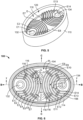
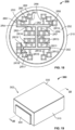
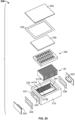
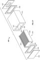
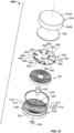
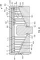
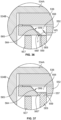
- the GDT 100 includes an insulator 110, a cover 130, a first terminal electrode 132, a second terminal electrode 134, a set E of inner electrodes E1-E14, an insulator 136, seals 135, 138, bonding layers 137, 139, a trigger device 150, and a selected gas M ( FIG. 6 ).
- the insulator 110 and the cover 130 collectively form an enclosure or housing 102 defining an enclosed GDT chamber 104 ( FIG. 6 ).
- the terminal electrodes 132, 134, the inner electrodes E1-E14, the insulator plate 136, the trigger device 150, and the gas M are contained in the chamber 104.
- the housing 102 has a central axis A-A ( FIG. 1 ), a first lateral axis B-B , and a second lateral axis C-C ( FIG. 6 ).
- the sixteen electrodes 132, 134, E1-E14 define a plurality of gaps G (fifteen gaps G) and a plurality of cells C (fifteen cells C) between the electrodes 132, 134, E1-E14 ( FIG. 6 ).
- the electrodes 132, 134 E1-E14 and the gaps G and cells C are serially distributed in spaced apart relation along the axis B-B .
- the insulator 110 may be generally cup-shaped.
- the insulator 110 includes an end or bottom wall 112 and an annular, elliptical, upstanding side wall 114 collectively defining a cavity 120 and a top opening 122 communicating with the cavity 120.
- Electrode through holes or openings 124 extend through the bottom wall 112. Integral locator features or tabs 116 project upwardly from the bottom wall 112.
- the insulator 110, the cavity 120 and the chamber 104 are elliptically shaped in cross-section perpendicular to the axis A-A.
- the insulator 110 may be formed of any suitable electrically insulating material.
- the insulator 110 may be formed of a material having a melting temperature of at least 1000 degrees Celsius and, in some cases, at least 1600 degrees Celsius.
- the insulator 110 is formed of a ceramic.
- the insulator 110 includes or is formed of alumina ceramic (Al 2 O 3 ), possibly at least about 90% Al 2 O 3 .
- the insulator 110 is monolithic.
- the electrodes 132, 134 each include a head 132A, 134A disposed in the cavity 120 and a contact post 132B, 134B extending through a respective opening 124 and projecting outwardly from the insulator 110.
- a bonding layer 137 is interposed between each post 132B, 134B and the inner surface of its opening 124.
- the posts 132B, 134B are bonded to the insulator 110 by the bonding layers 137 continuously about the full peripheries of the openings 124.
- the bonding layers 137 along with the seals 138 hermetically seal the openings 124.
- the bonding layers 137 are metallization, solder or metal-based layers. Suitable metal-based materials for forming the bonding layers 137 may include nickel-plated Ma-Mo metallization. Suitable materials for the seals 138 may include silver-copper alloy.
- the electrodes 132, 134 may be formed of any suitable material.
- the electrodes 132, 134 are formed of metal and, in some cases, are formed of molybdenum or Kovar. According to some versions, each of the electrodes 132, 134 is unitary and, in some cases, monolithic.
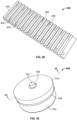
- the inner electrodes E1-E14 are serially positioned and distributed in the cavity 120 along the axis B-B .
- the electrodes E1-E14 are positioned such that each electrode E1-E14 is physically spaced apart from the immediately adjacent other inner electrode(s) E1-E14, 132, 134.
- the lower edge of each electrode E1-E14 is captured in slots defined between associated ones of the locator tabs 116 to thereby limit lateral displacement of the electrode E1-E14 relative to the housing 102.
- Each electrode E1-E14 is also captured between the bottom wall 112 and the trigger device 150 to thereby limit axial displacement (along axis A-A) of the electrode E1-E14 relative to the housing 102.
- each electrode E1-E14 is positively positioned and retained in position relative to the housing 102 and the other electrodes E1-E14, 132, 134.
- the electrodes E1-E14 are secured in this manner without the use of additional bonding or fasteners applied to the electrodes E1-E14.
- the electrodes E1-E14 may be semi-fixed or loosely captured between the locator features 116, the bottom wall 112 and the triggering device 150.
- the electrodes E1-E14 may be capable of floating up and down to a limited degree within the housing 102.
- each electrode E1-E14 is each arcuate, bent or curved plates. More particularly, each electrode E1-E14 has an arcuate, or curvilinear cross-sectional shape or profile in the plane defined by the lateral axes B-B and C-C, and is straight, flat or linear in planes parallel to the plane defined by the axes A-A and C-C.
- the opposing surfaces of the electrodes E1-E14 extend substantially parallel to one another. This configuration permits a greater gap length within a housing 102 of a given width and for the electrodes to have similar lengths.
- the electrodes E1-E14 may be formed of any suitable material. In some csases the electrodes E1-E14 are formed of metal, which may be molybdenum, copper, tungsten or steel. According to some versions, each of the electrodes E1-E14 is unitary and, in some cases, monolithic.
- each of the electrodes E1-E14 has a thickness T1 ( FIG. 6 ) in the range of from about 0.3 to 2 mm, perhpas in the range of from about 0.5 to 1 mm.
- Each electrode E1-E14 may have a height H1 ( FIG. 7 ) in the range of from about 1 to 20 mm and, in some cases, in the range of from 3 to 10 mm. According to some exaples, the length of each electrode E1-E14 is in the range of from about 10 to 50 mm.
- the insulator 136 may be shaped as a flat plate or otherwise configured.
- the insulator 136 may be formed of any suitable electrically insulating material.
- the insulator 136 is formed of a material having a melting point of at least 1000 degrees Celsius, possibly at least 1600 degrees Celsius.
- the insulator 136 may be formed of a ceramic, and may include or be formed of alumina ceramic (Al 2 O 3 ), in some cases at least about 90% Al 2 O 3 . In some cases, the insulator 136 is monolithic.
- the cover plate 130 may be shaped as a flat plate or otherwise configured.
- the cover plate 130 may be formed of any suitable material.
- the cover plate 130 can be formed of metal and, in some cases, is formed of copper or Kovar. In some version the cover plate 130 is unitary and, in some cases, monolithic.
- An annular bonding layer 139 is interposed between an annular top edge surface 118 of the insulator 110 and the lower surface of the cover 130.
- the seal 135 is interposed between the bonding layer 139 and the cover 130.
- the cover 130 is bonded to the surface 118 by the bonding layer 139.
- the bonding layer 139 may be formed of the same material as described above for the bonding layer 137.
- the seal layer 135 may be formed of the same material as described above for the seals 138.
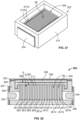
- the trigger device 150 ( FIGS. 3 , 4 and 7 -9) includes a substrate 152, a plurality of resistor links R1-R14 ( FIG. 8 ), and a conductor link 162.
- the resistor links R1-R14 and the conductor link 162 constitute a trigger circuit 151.
- the substrate 152 includes a body 154 and an integral annular flange 156.
- Recesses 158 are defined in the top side 154A of the body 154 and communicate with through holes 159 that extend to the bottom side 154B of the body 154.
- a channel 157 is also defined in the top side 154A.
- the substrate 152 may be formed of any suitable electrically insulating material.
- the substrate 152 is formed of a material having a melting temperature of at least 1000 degrees Celsius and, in some cases, at least 1600 degrees Celsius.
- the substrate 152 may be formed of a ceramic.
- the substrate 152 includes or is formed of alumina ceramic (Al 2 O 3 ), posisbily at least about 90% Al 2 O 3 .
- the substrate 152 is monolithic.
- each resistor link R1-R14 includes a resistor layer 164 and a terminal interface layer 160.
- Each resistor link R1-R14 is terminated on one end by the connecting layer 162 and by its terminal interface layer 160 on its opposing end.
- the terminal interface layers 160 are thereby electrically connected to the connecting layer through the resistor layers 164.
- the terminal interface layers 160 are bonded to the top surface of the substrate 152 in respective ones of the recesses 158.
- the terminal interface layers 160 extend to and may extend into the through holes 159.
- the connecting layer 162 may be formed of any suitable material.
- the connecting layer 162 may be formed of metal and, in some cases, is formed of metal in an adhesive carrier.
- the carrier can be a silicate-based adhesive carrier such as a sodium silicate or potassium silicate adhesive.
- the connecting layer 162 has a thickness in the range of from about 50 to 1000 micrometers.
- the terminal interface layers 160 may be formed of any suitable material.
- the terminal interface layers 160 may be formed of metal and, in some cases, are formed of metal in an adhesive carrier.
- the carrier can be a silicate-based adhesive carrier such as a sodium silicate or potassium silicate adhesive.
- each of the terminal interface layers 160 has a thickness in the range of from about 50 to 1000 micrometers.
- the resistor layers 164 may be formed of any suitable electrically resistive material. According to some versions, the resistor layers 164 are formed of graphite-based compound. In some cases, the resistor layers 164 are formed of a compound including graphite in an adhesive carrier.
- the carrier can be a silicate-based adhesive carrier such as a sodium silicate or potassium silicate adhesive.
- the resistor layers 164 may be formed of a material having a specific electrical resistance in the range of from about 1 micro-ohm-meter to 1 ohm-meter.
- Each of the resistor links R1-R14 may have an electrical resistance in the range of from about 3 to 500 ohms.
- Each of the resistor layers 164 may have a thickness in the range of from about 1 to 150 micrometers.
- the gas M may be any suitable gas, and may be a single gas or a mixture of two or more (e.g., 2, 3, 4, 5, or more) gases. In some cases, the gas M includes at least one inert gas.
- the gas M may include at least one gas selected from argon, neon, helium, hydrogen, and/or nitrogen. In some cases, the gas M is or includes helium.
- the gas M may be air and/or a mixture of gases present in air.
- the gas M may comprise a single gas in any suitable amount, such as, for example, in any suitable amount in a mixture with at least one other gas.
- the gas M may comprise a single gas in an amount of about 0.1%, 0.5%, 1%, 5%, 10%, 15%, 20%, 25%, 30%, 35%, 40%, 45%, 50%, 55%, 60%, 65%, 70%, 75%, 80%, 85%, 90%, 95%, 98%, or 99% by volume of the total volume of gas present in the GDT chamber 104, or any range therein.
- the gas M may comprise a single gas in an amount of less than 50% (e.g., less than 40%, 30%, 20%, 10%, 5%, or 1%) by volume of the total volume of gas present in the GDT chamber 104. In some cases, the gas M may comprise a single gas in an amount of more than 50% (e.g., more than 60%, 70%, 80%, 90%, or 95%) by volume of the total volume of gas present in the GDT chamber 104. In some cases, the gas M may comprise a single gas in an amount in a range of about 0.5% to about 15%, about 1% to about 50%, or about 50% to about 99% by volume of the total volume of gas present in the GDT chamber 104.
- the gas M comprises at least one gas present in an amount of at least 50% by volume of the total volume of gas present in the GDT chamber 104.
- the gas M comprises helium in an amount of at least 50% by volume of the total volume of gas present in the GDT chamber 104.
- the gas M comprises at least one gas present in an amount of about 90% or more by volume of the total volume of gas present in the GDT chamber 104, and, in some cases, in an amount of about 100% by volume of the total volume of gas present in the GDT chamber 104.
- the gas M may comprise a mixture of a first gas and a second gas (e.g., an inert gas) different from the first gas with the first gas present in an amount of less than 50% by volume of the total volume of gas present in the GDT chamber 104 and the second gas present in an amount of at least 50% by volume of the total volume of gas present in the GDT chamber 104.
- the first gas is present in an amount in a range of about 5% to about 20% by volume of the total volume of gas present in the GDT chamber 104 and the second gas is present in an amount of about 50% to about 90% by volume of the total volume of gas present in the GDT chamber 104.
- the first gas is present in an amount of about 10% by volume of the total volume of gas present in the GDT chamber 104 and the second gas is present in an amount of about 90% by volume of the total volume of gas present in the GDT chamber 104.
- the second gas is helium, which may be present in the proportions described above for the second gas.
- the first gas (which may be present in the proportions described above for the first gas) is selected from the group consisting of argon, neon, hydrogen, and/or nitrogen, and the second gas is helium (which may be present in the proportions described above for the second gas).
- the GDT 100 may be assembled as follows.
- the terminal electrodes 132 and 134 are inserted through the openings 159.
- the bonding layers 137 are heated to bond the terminals 132, 134 to the insulator 110 in the openings 124.
- the seals 138 are installed or formed about the posts 132B, 134B to secure the electrodes 132, 134 in place and hermetically seal the openings 159.
- the seals 138 are metal solder or brazings, which may be formed of silver-copper alloy, for example.
- the inner electrodes E1-E14 are installed in the cavity 120. More particularly, the electrodes E1-E14 are each installed in a respective set of slots between the locator features 116 as shown in FIG. 6 .
- the trigger device 150 is placed over the inner electrodes E1-E14 so that the bottom side 154B rests on the top edges 142A ( FIG. 7 ) of the inner electrodes E1-E14.
- the trigger device 150 is aligned such that the through holes 159 are each aligned with a respective one of top edges 142A of the electrodes E1-E14, 134, and the interface layers 160 therein are located on or closely adjacent said respective top edges 142A.
- the insulator plate 136 and the cover 130 are then placed over the trigger device 150.
- the cover 130 is bonded to the top face 118 of the insulator 110 to form the housing 102 and gas-tight sealed chamber 104.
- the cover 130 is sealingly secured to the insulator 110 by brazing or heating the cover 130 and thereby melt-bonding the bonding layer 139 to the cover 130.
- the bonding layer 139 may be sprayed onto or otherwise applied to the insulator 110.
- the components of the GDT 100 are disposed in an assembly chamber during the steps of placing the cover 130 on the insulator 110 and securing the cover 130 to the insulator 110 to enclose and seal the chamber 104.
- the assembly chamber is filled with the gas M at a prescribed pressure and temperature.
- the gas M is thereafter captured and contained in the chamber 104 of the assembled GDT 100 at a prescribed pressure and temperature.
- the prescribed pressure and temperature are selected such that the gas M is present at a desired operational pressure when the GDT 100 is installed and in use at a prescribed service temperature.
- the pressure of the gas M in the chamber 104 of the assembled GDT 100 is in the range of from about 50 to 1000 mbar at 20 degrees Celsius.
- the relative dimensions of the insulator 110, the electrodes E1-E14, the trigger device 150, the insulator plate 136, and the cover 130 are selected such that the electrodes E1-E14 are loosely captured between the substrate 152 and the insulator bottom wall 112 to permit the electrodes E1-E14 to slide up and down a small distance.
- the permitted vertical float distance is in the range of from about 0.05 to 0.5 mm.
- the substrate 152 and the bottom wall 112 fit snuggly against or apply a compressive load to the electrodes E1-E14.
- the electrodes 132, E1-E14, 134 define a plurality of gaps G and a plurality of cells C between each pair of electrodes 132, E1-E14, 134.
- the minimum width W1 ( FIG. 6 ) of each gap G i.e., the smallest gap distance between the two electrode surfaces forming the cell C
- W1 is in the range of from about 0.2 to 1.5 mm.
- the through holes 159 associated with the resistor links R1-R14 are positioned over the top edges 142A, 134C of the electrodes E1-E14 and 134, respectively.
- the terminal layer 160 of each resistor link R1-R14 is positioned on or closely adj acent the corresponding top edge 142A, 134C through the corresponding through hole 159.
- the resistor links R1-R14 are electrically coupled to the electrodes E1-E14, 134 through their respective terminal layers 160. Because the electrodes E1-E14 are floating or not fully fixed in the housing 102 and the terminal electrode 134 is spaced from the trigger device 150, it may not be possible to ensure tight contact between the resistor links R1-R14 and the electrodes E1-E14, 134. As a result, a small gap J ( FIG. 7 ) may be present between each resistor link R1-R14 and its electrode E1-E14, 134. According to some cases, each gap J has a width in the range of from about 0 to 0.5 mm.
- this gap J may cause sparking between the resistor link R1-R14 and the electrode E1-E14, 134. If the sparking is applied to the resistor layer 164, such sparking may damage the resistor layer 164, which may in turn enlarge the gap and adversely affect performance of the GDT 100 ( e . g ., increase the required spark over voltage).
- the terminal interface layers 160 can prevent or reduce such damage to the resistor links R1-R14 and thereby improve the performance and service life of the GDT 100.
- the material of the terminal interface layers 160 has an electrical conductivity substantially the same as the electrode and greater than that of the resistor layer 164 so that the aforementioned sparking is eliminated or reduced. Moreover, the material of the terminal interface layers 160 may be more resistant to degradation from etching than the material of the resistor layer 164.
- the plurality of spark gaps G are housed or enveloped in the same housing 102 and chamber 104.
- the plurality of cells C and spark gaps G defined between the electrodes 132, E1-E14, 134 are in fluid communication so that they share the same mass or volume of gas M.
- the size and number of parts can be reduced.
- the size, cost and reliability of the GDT 100 can be reduced as compared to a plurality of individual GDTs connected in series.
- the trigger device 150 including the trigger circuit 151 is housed or enveloped in the same housing 102 and chamber 104 as the electrodes 132, E1-E14, 134, and is likewise in fluid communication with the same mass of gas M.
- the size, cost and reliability of the GDT 100 can be reduced as compared to a plurality of individual GDTs connected in series with an external trigger circuit.
- the arcuate configurations of the electrodes E1-E14 can help to ensure that, in the case of a surge event, spark over occurs between the midsections of the electrodes E1-E14, not at their edges.
- the floating or semi-fixed mounting of the electrodes E1-E14 in the housing 102 can facilitate ease of assembly.
- the performance attributes of the GDT 100 can be determined by selection of the gas M, the pressure of the gas M in the chamber 104, the dimensions and geometries of the electrodes 132, E1-E14, 134, the geometry and dimensions of the housing 102, the sizes of the gaps G, and/or the electrical resistances of the resistor links R1-R14.
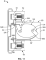
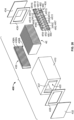
- an electrical assembly 5 is shown therein.
- the electrical assembly 5 incorporates the GDT 100.
- the GDT 100 is mounted in an enclosure 52 of a GDT module 50 that is removeably and replaceably mounted on a base 60.
- the base 60 is in turn mounted on a support DR to mechanically and electrically connect the GDT 100 to an electrical power system.
- the support DR is a DIN rail.
- the base 60 includes an enclosure 62, a first electrical connector 64 to which a first electrical wire WL (e.g ., a line wire) is secured and a second electrical connector 66 to which a second electrical wire WN (e.g. , a neutral wire) is secured.
- the GDT module 50 includes a jumper 54 including connectors 54A and 54B.
- the connector 54A is secured to the terminal electrode 132 and the connector 54B is releasably interlocked with the base connector 64.
- the GDT module 50 further includes a second jumper 56 including connectors 56A and 56B.
- the connector 56A is secured to the terminal electrode 134 and the connector 56B is releasably interlocked with the base connector 66.
- the jumper 56 may further include a thermal disconnector mechanism 56D.
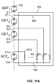
- FIG. 11A is an electrical schematic circuit of a modular, multi-cell gas discharge tube 100 as illustrated in FIGS. 1-9 .
- the modular, multi-cell gas discharge tube 100 may include a plurality of single cell GDTs that are arranged serially between terminals 132 and 134.
- a first terminal 132 and the inner electrode E1 may function as a first single cell GDT 1
- the inner electrode E1 and the inner electrode E2 may function as a second single cell GDT 2 that is serially connected to the first single cell GDT 1 and so on.
- a trigger circuit 150 may include multiple resistors R1-R14 that may be connected between respective ones of the inner electrodes E1-E14 and the terminal 134.
- the resistors R1-R14 include resistive layers 164 and are electrically conductively coupled to the connecting layer 162 and interface layers 160.
- the modular, multi-cell gas discharge tube 100 provides that the interface layers 160 are electrically conductively coupled to the inner electrodes E1-E14.
- the first terminal 132 may be connected to a line or phase voltage of a single or multi-phase power system and the second terminal 134 may be connected to a neutral line of the single or multi-phase power system.
- the total arcing voltage of the modular, multi-cell gas discharge tube 100 generally corresponds to the sum of the arcing voltage of individual series connected single cell GDTs and thus exceeds the peak value of the system voltage.
- the current flowing therethrough will be generally limited to the current corresponding to a surge event, such as lightning, and not from the system source.
- the overvoltage is applied to GDT 2 , which then begins to conduct.
- GDT 3 the overvoltage is applied to GDT 3 , which then begins to conduct.
- resistor R2 will conduct a small amount of current once GDT 2 begins conducting until GDT 3 begins to conduct.
- the GDTs stay in conduction mode until the overvoltage condition has ceased. Once the overvoltage condition ceases, the GDTs cease to conduct because the peak value of the system voltage is less than the total arcing voltage of the modular, multi-cell gas discharge tube 100.
- the quantity of gaps in the modular, multi-cell gas discharge tube 100 may vary depending on the operating voltage of the system. For example, for a 255V application, a modular, multi-cell gas discharge tube 100 may use between 14 and 21 total gaps between the terminal 132, the inner electrodes E1-E14 and the terminal 134. Some cases provide that the quantity of gaps may be less than 14 if the system voltage is correspondingly less than the examples provided herein and the quantity of gaps may be greater than 21 if the system voltage is correspondingly greater than the examples provided herein.
- the resistance values of resistors R1-R14 may be in a range between about 3 Ohms to about 500 Ohms, however, such cases are non-limiting and the resistance values may be less than 3 Ohms and/or greater than 500 Ohms. In some cases, the resistance values of resistors R1-R14 may all be the same, while in other cases the resistor values of resistors R1-R14 may be different from one another.
- FIG. 11B is an electrical schematic circuit of a modular, multi-cell gas discharge tube 100 as illustrated in FIGS. 1-9 .
- Many elements as discussed above regarding FIG. 11A are substantially the same and thus duplicative discussion thereof will be omitted.
- an additional gap corresponding to GDT n may be added in series with the circuit of FIG. 11A .
- GDTi a single GDT
- both GDT 1 and GDT n must begin conducting to trigger the conduction of the other GDTs.
- An advantage of having both GDT 1 and GDT n to begin conducting is that if either of GDT 1 or GDT n short circuit or begin to degrade, a gap will still be present in the other GDT and the device may still function. Such advantage may provide increased safety in operation, although response time may be increased.
- the GDT 200 includes an insulator 210, a cover 230, a first terminal electrode 232, a second terminal electrode 234, a set 2E of inner electrodes 2E1-2E19, an insulator 236, seals 235, 238, bonding layers 237, 239, a trigger device 250, and a selected gas M corresponding to the insulator 110, the cover 130, the first terminal electrode 132, the second terminal electrode 134, the inner electrodes E1-E14, the insulator 136, the seals 135, 138, the bonding layers 137, 139, the trigger device 150, and the selected gas M of the GDT 100, except as follows.
- the electrodes 2E1-2E19, the trigger device 250, and the gas M are all contained in a hermetically sealed chamber 204 in a housing 202 formed by the insulator 210 and the cover 230.
- the insulator 210 includes an integral ceramic partition wall 215 that bisects the cavity 220.
- the partition wall 215 divides the cavity 220 into subcavities 220A, 220B.
- the substrate 252 of the trigger device 250 includes an integral ceramic rib 252A that is received in a groove 215A defined in the top edge of the partition wall 215.
- the insulator 210, the cavity 220 and the chamber 204 are cylindrically shaped.
- terminal electrodes 232, 234 are secured and sealed by the bonding layers 237 and the seals 238 in openings 224 on the same lateral end of the cavity 220 and opposite sides of the partition wall 215.
- the arcuate inner electrodes 2E1-2E9 are secured in the subcavity 220A and the arcuate inner electrodes 2E11-2E19 are secured in the subcavity 220B.
- the inner electrode 2E10 includes an integral first portion 244A in the subcavity 220A and an integral second portion 244B in the subcavity 220B.
- the electrode portions 244A, 244B are connected by an integral connecting portion 244C that extends through a slot 220C defined between the sidewall 214 and an end of the partition wall 215.
- the electrodes 2E1-2E19 are each arcuate, curved or bent plates that are curvilinear in lateral profile and straight in axial profile.
- the electrodes 2E1-2E19 are captured to be semi-fixed or floating by the locator features 216, the sidewall 214 and the partition wall 215.
- the trigger device 250 includes a ceramic substrate 252, connecting layers 262, and resistor links 2R2-2R19 corresponding to the ceramic substrate 152, connecting layers 162, and resistor links R1-R14 of the GDT 100.
- the terminal interface layers 260 of the first connecting layer 262 and the resistor links 2R2-2R19 are positioned on or closely adjacent the top edges of the electrodes 2E1-2E19 and 234, respectively, through the through holes 259 in the substrate 252.
- the GDT 200 includes twenty spark gaps G and twenty cells C.
- spark over occurs sequentially from the electrode 232, through the electrodes 2E1-2E19 and to the electrode 234. Spark over directly between the electrodes 2E1-2E9 in the subcavity 220A and the electrodes 2E11-2E19 in the subcavity 220B is prevented by the electrically insulating partition wall 215 and rib 252A.
- the trigger device 250 operates in the same manner as described above with regard to the trigger device 150 to control the firing sequence and timing.
- the GDT 300 includes an insulator 310, a cover 330, a first terminal electrode 332, a second terminal electrode 334, a set 3E of inner electrodes 3E1-3E18, an insulator 336, seals 335, 338 bonding layers 337, 339, a trigger device 350, and a selected gas M corresponding to the insulator 110, the cover 130, the first terminal electrode 132, the second terminal electrode 134, the inner electrodes E1-E14, the insulator 136, the seals 135, 138, the bonding layers 137, 139, the trigger device 150, and the selected gas M of the GDT 100, except as follows.
- the electrodes 3E1-3E18, the trigger device 350, and the gas M are all contained in a hermetically sealed chamber 304 in a housing 302 formed by the insulator 310 and the cover 330.
- the insulator 310 includes integral ribs 317A defining locator slots 317B therebetween. Opposed end openings 324 communicate with the cavity 320.
- the insulator 310, the cavity 320 and the chamber 304 are rectangular in cross-section.
- the terminal electrodes 332 and 334 are secured and sealed by the bonding layers 337 in the openings 324.
- the inner electrodes 3E1-3E18 are substantially flat plates with opposed planar faces. The electrodes 3E1-3E18 are seated in the slots 317B and thereby semi-fixed or floatingly mounted in the chamber 304.
- the trigger device 350 includes a ceramic substrate 352, connecting layers 362, and resistor links 3R2-3R18 corresponding to the ceramic substrate 152, connecting layers 162, and resistor links R1-R14 of the GDT 100.
- the terminal interface layers 360 of the connecting layer 362 and the resistor links 3R2-3R18 are positioned on or closely adjacent the top edges of the electrodes 3E1-3E18 and 334, respectively, through the through holes 359 in the substrate 352.
- the GDT 300 includes nineteen spark gaps G and nineteen cells C. In use, spark over occurs sequentially from the electrode 332, through the electrodes 3E1-3E18 and to the electrode 334.
- the trigger device 350 operates in the same manner as described above with regard to the trigger device 150 to control the firing sequence and timing.
- the GDT 400 includes an insulator 410, a first terminal electrode 432, a second terminal electrode 434, a set 4E of inner electrodes 4E1-4E18, an insulator 436, bonding layers 437, seals 438, a trigger device 450, and a selected gas M corresponding to the insulator 110, the first terminal electrode 132, the second terminal electrode 134, the inner electrodes E1-E14, the insulator 136, the bonding layer 137, the seal 138, the trigger device 150, and the selected gas M of the GDT 100, except as follows.
- the electrodes 4E1-4E18, the trigger device 450, and the gas M are all contained in a hermetically sealed chamber 404 in a housing 402 formed by the insulator 410 and the electrodes 432, 434.
- the insulator 410 is generally tubular and has opposed end openings 424 communicating with the cavity 420.
- the insulator 410, the cavity 420 and the chamber 404 are rectangular in cross-section.
- the insulator 436 is a plate having integral ribs 436A defining locator slots 436B therebetween.
- the trigger device 450 includes a ceramic substrate 452, connecting layers 462, and resistor links 4R1-4R18 corresponding to the ceramic substrate 152, connecting layers 162, and resistor links R1-R18.
- the substrate 452 includes integral ribs 453B defining locator slots 453B therebetween.
- the inner electrodes 4E1-4E18 are substantially flat plates with opposed planar faces.
- the inner electrodes 4E1-4E18 are seated in the slots 436B of the insulator plate 436 on one side edge and are seated in the slots 453B of the trigger device 450 on the side edge to form a cassette or subassembly 403 as shown in FIG. 27 .
- the subsassembly 403 is inserted into the cavity 420 through the opening 424.
- the terminal electrodes 432 and 434 are secured and sealed by the bonding layers 437 in the openings 424.
- the inner electrodes 4E1-4E18 are semi-fixed or floatingly secured in the sealed chamber 404 by the locator ribs 436A, 453A and the top and bottom walls of the insulator 410.
- the terminal interface layers 460 of the resistor links 4R1-4R18 are positioned on or closely adjacent the top edges of the electrodes 4E1-4E18 and 434, respectively, through the through holes 459 in the substrate 452.
- the GDT 400 includes nineteen spark gaps G and nineteen cells C. In use, spark over occurs sequentially from the electrode 432, through the electrodes 4E1-4E18 and to the electrode 434.
- the trigger device 450 operates in the same manner as described above with regard to the trigger device 150 to control the firing sequence and timing.
- the GDT 500 includes an insulator 510, a first terminal electrode 532, a second terminal electrode 534, a set 5E of inner electrodes 5E1-5E7, an insulator 536, a seal 538, bonding layers 537, 539, a trigger device 550, and a selected gas M corresponding to the insulator 110, the first terminal electrode 132, the second terminal electrode 134, the inner electrodes E1-E14, the insulator 136, the seals 138, the bonding layers 137, 139, the trigger device 150, and the selected gas M of the GDT 100, except as follows.
- the electrodes 5E1-5E7, the trigger device 550, and the gas M are all contained in a hermetically sealed chamber 504 in a housing formed by the insulator 510 and the electrode 534.
- the electrode 534 serves as a cover.
- the insulator 510 includes an electrode opening 524 within which the terminal electrode 532 is secured and hermetically sealed by a seal 538 and the bonding layer 537.
- the insulator 510 includes a series of concentric, annular steps 519. The steps 519 progressively increase in height in the direction from the terminal electrode 532 to the side wall 514.
- the insulator 510, the cavity 520 and the chamber 504 are tubular or cylindrically shaped.
- the terminal electrode 534 includes an end wall 534A and an annular side wall 534B.
- the side wall 534B is secured to the side wall 514 of the insulator 510 by the bonding layer 539.
- the interface between the terminal electrode 534 and the side wall 514 is hermetically sealed by a seal 538 and the bonding layer 539.
- the inner electrodes 5E1-5E7 are cylindrical and concentrically mounted on respective ones of the steps 519 in the chamber 504.
- the inner electrodes 5E1-5E7 are radially spaced apart to define annular spark gaps G and cells C therebetween.
- the electrodes 5E1-5E7 are radially constrained by the steps 519 and axially constrained by the insulator bottom wall 512 and the trigger device 550 so that the electrodes are semi-fixed or floating in the chamber 504.
- the trigger device 550 is in turn constrained by the insulator plate 536 and the terminal electrode 534.
- the trigger device 550 includes a ceramic substrate 552 and resistor links 5R1-5R7 corresponding to the ceramic substrate 152 and resistor links R1-R14 of the GDT 100.
- the terminal interface layers 560 of the resistor links 5R1-5R7 are positioned in recesses 558 and on or closely adjacent the top edges of the electrodes 5E1-5E7 and 534, respectively, through the through holes 559 in the substrate 552.
- Each resistor link 5R1-5R7 includes a terminal contact 565 on its end opposite its terminal interface layer 560.
- the resistor links 5R1-5R7, respectively, are electrically connected to the electrode 534 via their respective terminal contacts 565. Small gaps may be present between the electrode 534 and some or all of the terminal contacts 565.
- the terminal contacts 565 are formed of a material as described above for the terminal interface layers 160 in order to prevent sparking and degradation of the resistor layers 564 of the resistor links 5R1-5R7 as discussed above with regard to the terminal interface layers 160 and the resistor layers 164.
- the GDT 500 includes eight spark gaps G and eight cells C. In use, spark over occurs sequentially from the electrode 532, through the electrodes 5E1-5E7 and to the electrode 534.
- the trigger device 550 operates in the same manner as described above with regard to the trigger device 150 to control the firing sequence and timing.
- the terminal interface layers 560 may be masses or plugs of the electrically conductive material that substantially fill the holes 559 as shown and described above with regard to the terminal interface layers 160 and with reference to FIG. 7 . As shown in FIG. 36 , the terminal interface layers 560 may take the form of relatively thin layers 560' and the through holes 559 may remain open. The terminal interface layers 160, 260, 360, 460 may likewise be formed in this manner. A gap J may be present between each or some of the terminal interface layers 560' and their respective electrodes 5E1-5E7. According to some cases, each of the gaps J has a width W5 of less than about 0.5 mm.
- each electrode 5E1-5E7 may include an integral contact protrusion or pin 557 projecting upwardly from its top edge.
- the pin 557 is received in a respective through hole 559 and extends into the associated recess 558.
- each terminal interface layer 560 takes the form of a terminal interface layer 560" that fills the space about the pin 557 in the recess 558.
- Each terminal interface layer 560" is bonded to its corresponding resistor layer 564 to the ceramic 552 and to the pin 557 to effect electrical and mechanical connection therebetween.
- the terminal interface layers 160, 260, 360, 460 may likewise be formed in this manner.
- This device may be manufactured by installing the pins 557 in the through holes 559, and then placing the material of the terminal interface layers 560" in the recesses 558 in molten or liquid form, after which the material solidifies (e.g ., by drying or cooling) or heating (sintering) and bonds to the resistor layer, ceramic and pin.
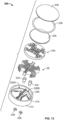
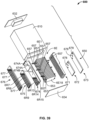
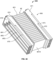
- FIGS. 38-44 a modular multi-cell GDT 600 according to an embodiment of the invention is shown therein. While FIGS. 38 and 39 are exploded views, the GDT 600 will outwardly appear substantially the same as the GDT 400 when assembled.
- the GDT 600 includes an insulator 610, a first terminal electrode 632, a second terminal electrode 634, a set 6E of inner electrodes 6E1-6E18 ( FIG.
- the GDT 600 further includes a multi-layered trigger device 650 corresponding to the trigger device 450.
- the trigger device 650 performs the same function as the trigger device 450 in generally the same manner, but is differently constructed in order to provide improved and/or more consistent and reliable performance.
- the inner electrodes 6E1-6E18 each include relatively short integral locator pins 653 ( FIGS. 38 and 39 ) projecting from one side edge, and relatively long integral electrical contact pins 657 projecting from their opposed side edges.
- the contact pins 657 have different lengths and are staggered in height along the electrode side edges.
- the trigger device 650 includes six discrete substrates 671, 672, 673, 674, 675, and 676.
- the substrates 671-676 may be formed in substantially the same manner and of the same material as the substrate 452.
- Each of the substrates 671-676 includes three longitudinally extending grooves 677 extending along a lengthwise axis I-I ( FIG. 44 ) from a proximal end 677A to an opposing distal end 677B ( FIG. 38 ).
- the distal ends 677B each terminate proximate, at or closely adjacent a distal end 679 of the substrate 671-676.
- Laterally extending through holes 678 extend fully through the thicknesses of the substrates 671-676.
- the through holes 678 are axially staggered.
- One of the holes 678 terminates proximate the proximal end 677A of each groove 677.
- the substrates 671 and 674 each include slots 617B corresponding to slots 417B to receive and to secure the inner electrodes 6E1-6E18.
- the substrates 671, 674 also include locator recesses 617C to receive the locator pins 653 to locate the electrodes 6E1-6E18 along the height axis.
- the substrate 671 includes axially distributed recesses 671A with a step 671B therebetween.
- the substrate 674 includes recesses 674A with a step 674B therebetween.
- a respective resistor link 6R1-6R18 ( FIGS. 39-42 ) is located in each groove 677.
- Each resistor link 6R1-6R18 includes a resistor layer 664 corresponding to the resistor layers 464, and terminal interface layers 660A, 660B corresponding to the terminal interface layers 460.
- the interface layers 660A are located at the through holes 678.
- the interface layers 660B are located at the distal ends 679.
- the trigger device 650 does not include a conductive link corresponding to the connecting layer 462.
- the second terminal electrode 634 ( FIG. 44 ) includes an outer contact section 634A, a trigger contact section 634B, and an electrode gap surface 634C.
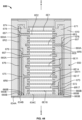
- the GDT 600 may be assembled in the same manner as the GDT 400, except as follows.
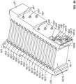
- the substrates 671 and 674 are mounted on either side of the set 6E of electrodes as shown in FIG. 40 .
- the edge portions of the electrodes 6E1-6E18 are received in the slots 617B of the substrates 671, 674 and the electrodes 6E1-6E18 are thereby captured between the substrates 671, 674.
- the locator pins 653 are seated in the locator recesses 617C.
- the contact pins 657 project through the holes 678.
- the three distal most contact pins 657 extend into the holes 678 the resistor links 6R16-6R18 of the substrate 671 such that they make contact with or are positioned closely adjacent to the interface layers 660A of the resistor links 6R16-6R18.
- the distalmost contact pins 657 extend into the holes 678 of the resistor links 6R13-6R15 of the substrate 674 such that they make contact with or are positioned closely adjacent the interface layers 660A of the resistor links 6R13-6R15.
- the substrate 672 is mounted in the lower recess 671A of the substrate 671 such that the middle three contact pins 657 on that side extend through the holes 678 in the substrate 672. These contact pins 657 make contact with or are located closely adjacent the interface layers 660A of the resistor links 6R10-6R12.
- the substrate 675 is mounted in the lower recess 674A of the substrate 674 such that the middle three contact pins 657 on that side extend through the holes 678 in the substrate 675.
- These contact pins 657 make contact with or are located closely adjacent to the interface layers 660A of the resistor links 6R7-6R9.
- the substrate 673 is mounted over the substrate 672 and in the upper recess 671A of the substrate 671.
- the three proximal contact pins 657 extends through the through holes 628 and the substrate 673 and make contact with or are positioned closely adjacent the interface layers 660A of the resistor links 6R4-6R6.
- the substrate 676 is mounted over the substrate 675 and in the upper recess 674A of the substrate 674.
- the three proximal contact pins 657 extend through the holes 678 in the substrate 676 and make contact with or are positioned closely adjacent to the interface layers 660A of the resistor links 6R1-6R3.
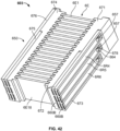
- a subassembly 603 as shown in FIGS. 42 and 43 is thus formed.
- the subassembly 603 is inserted in the passage 620 of the housing 610.
- the terminal electrodes 632, 634 are secured to the housing 610 on either end.
- the substrate distal ends 679 are located adjacent the terminal electrode section 634A so that the distal interface layers 660B are located in contact with or closely adjacent the section 634A.
- the terminal electrode section 634C is positioned at a prescribed distance from the inner electrode 6E18 define a gap G.
- each of the inner electrodes 6E1-6E18 is electrically connected directly to the terminal electrode 634 through its respective contact pin 657 and its respective resistor link 6R1-6R18.
- the resistor links 6R1-6R18 (and, in particular, the resistor layers 664 thereof) are relatively layered so that the resistor links of each substrate 671-676 lie in different longitudinally and heightwise extending planes, which planes are laterally spaced apart.
- the substrates 671-676 electrically insulate the resistor links 6R1-6R18 from one another.
- the multi-layered trigger device 650 can provide certain advantages.
- the resistor layers 664 of each of the resistor links 6R1-6R18 can be formed of sufficient length to reliably provide electrical resistance that is sufficiently high and stable for the intended operation. Also, by eliminating the connecting layer 462, the risk of unintended electrical resistance in that layer ( e.g ., caused by damage in use) can be eliminated.
- the trigger device 650 can be constructed to have robust electrical performance while also permitting the compact form factor and other advantages ( e . g ., in manufacture) of the rectangular GDT configuration.
- the gas M includes helium gas in a significant proportion, the arc voltage between adjacent electrodes is significantly increased as compared to when other commonly used gases are used, while maintaining substantially the same or a similar overall protection level voltage for the GDT device.
- the GDT can be constructed with fewer inner electrodes and cells, which permits the GDT to be formed with a smaller size and fewer parts in the GDT.
- the gas M includes helium in an amount at least 50% by volume of the total volume of gas present in the GDT chamber ( e . g ., the chamber 104, 204, 304, 404, 504, or the chamber of the GDT 600).
- a GDT containing a gas M including helium as described is electrically connected between a line or phase voltage of a single or multi-phase power system or circuit and a neutral line of the single or multi-phase power system or circuit.
- a gas medium including helium gas may be used in each one of a group or set of serially electrically connected single-cell GDTs (e.g., of otherwise known design) that are arranged to provide an overvoltage protection circuit.
- each single-cell GDT may include its own respective housing defining its own individual sealed GDT chamber, and the helium-containing gas mediums are present in each GDT chamber between the electrodes of the respective GDT (i.e., the gas is not shared between fluidly communicating cells as in the multi-cell GDTs described herein).
- the overvoltage protection circuit may include an external trigger device operative to serially trigger the cells of the linked single-cell GDTs.
- an overvoltage protection circuit including helium-containing gases as described is electrically connected between a line or phase voltage of a single or multi-phase power system or circuit and a neutral line of the single or multi-phase power system or circuit.
- the terminal interface layers e . g ., layers 160, 260, 360, 460, 560, 560', 560", 660A, 660B
- the connecting layers e . g ., layer 162
- the compound is applied to the substrate ( e . g ., substrate 152) and then dries and becomes solid to form the respective terminal interface layer or connecting layer bonded to the substrate and resistor layer.
- the liquid phase carrier is liquid sodium silicate in liquid phase.
- GDTs 100-600 have been shown and described herein having certain numbers of inner electrodes ( e . g ., electrodes E1-E14), GDTs according to embodiments of the invention may have more or fewer inner electrodes.
- a GDT as disclosed herein has at least two inner electrodes defining at least three spark gaps G and, in some embodiments, or at least three inner electrodes defining at least four spark gaps G.
- the terminal electrodes and the inner electrodes may have different shapes than those shown in the figures.
- the inner electrodes E1, E14, 2E1, 2E19 nearest the terminal electrodes 132, 134, 232, 234 are annular or cylindrical. This configuration can enlarge the active area of the inner electrodes to conduct current from the terminal electrodes.
Landscapes
- Engineering & Computer Science (AREA)
- Manufacturing & Machinery (AREA)
- Gas-Filled Discharge Tubes (AREA)
- Plasma Technology (AREA)
- Lasers (AREA)
- Treating Waste Gases (AREA)
- Gas Separation By Absorption (AREA)
- Incineration Of Waste (AREA)
- Thermistors And Varistors (AREA)
- Spark Plugs (AREA)
Claims (13)
- Eine Gasentladungsröhre (600), umfassend:ein Gehäuse (610), das eine Kammer definiert;eine erste und zweite Anschlusselektrode (632, 634), die auf dem Gehäuse angebracht sind;eine Vielzahl von inneren Elektroden (6E1-6E18), die in der Kammer liegt;ein Gas (M), das in der Kammer enthalten ist;wobei die inneren Elektroden in der Kammer in einer beabstandeten Beziehung seriell angeordnet sind, um eine Serie von Funkenspalten (G) von der ersten Anschlusselektrode zur zweiten Anschlusselektrode zu definieren;wobei die Kammer hermetisch abgedichtet ist;wobei die Gasentladungsröhre ferner eine Auslösevorrichtung (650) umfasst, die in dem Gehäuse enthalten ist und die entweder mit einer der ersten Anschlusselektrode (632) oder der zweiten Anschlusselektrode (634) und mit jeweiligen der Vielzahl von inneren Elektroden (6E1-6E18) elektrisch gekoppelt ist;wobei die Auslösevorrichtung Folgendes beinhaltet:ein erstes und zweites Substrat (672, 673), die jeweils aus einem elektrisch isolierenden Material gebildet sind;mindestens eine Widerstandsstrecke (6R10-6R12), die auf dem ersten Substrat angebracht ist; undmindestens eine Widerstandsstrecke (6R4-6R6), die auf dem zweiten Substrat angebracht ist; undwobei die Widerstandsstrecken dazu konfiguriert sind, Strom von den inneren Elektroden (6E1-6E18) zu leiten.
- Gasentladungsröhre nach Anspruch 1, wobei die Auslösevorrichtung (650) Löcher (678) beinhaltet, die in dem Substrat (652) definiert sind, um eine elektrische Verbindung zwischen den Widerstandsstrecken (6R2-6R18) und den inneren Elektroden (6E1-6E18) zu gestatten.
- Gasentladungsröhre nach Anspruch 2, wobei:
jede der Widerstandsstrecken (6R2-6R18) ferner Folgendes beinhaltet:eine Widerstandsschicht (664), die an ihr Substrat gebondet ist, wobei die Widerstandsschicht aus einem elektrisch widerstandsfähigen Material gebildet ist; undeine Anschlussschnittstellenschicht (660) zwischen der Widerstandsschicht (664) davon und der mit der Widerstandsstrecke assoziierten inneren Elektrode; unddie Anschlussschnittstellenschicht (660) aus Metall gebildet ist. - Gasentladungsröhre nach Anspruch 3, wobei:die Auslösevorrichtung (650) Löcher (659) beinhaltet, die in dem Substrat (652) definiert sind; undjede der Anschlussschnittstellenschichten (660) auf einer j eweiligen oder dicht angrenzend an eine jeweilige der inneren Elektroden (6E1-6E18) durch ein jeweiliges der Löcher (659) liegt, um die Widerstandsstrecken (6R2-6R18) mit den inneren Elektroden (6E1-6E18) elektrisch zu verbinden.
- Gasentladungsröhre nach Anspruch 4, wobei zwischen mindestens einer der Anschlussschnittstellenschichten (660) und ihrer entsprechenden angrenzenden inneren Elektrode (6E1-6E18) ein Spalt (J) definiert ist.
- Gasentladungsröhre nach Anspruch 3, wobei jede der Anschlussschnittstellenschichten (660) eine Dicke im Bereich von etwa 50 bis 1000 Mikrometer aufweist.
- Gasentladungsröhre nach Anspruch 1, wobei die Auslösevorrichtung (650) integrale Fixierungsmerkmale (617) beinhaltet, die die inneren Elektroden (6E1-6E18) in der Kammer sichern, während sie eine Verschiebung zwischen dem Gehäuse und den inneren Elektroden begrenzen.
- Gasentladungsröhre nach Anspruch 1, wobei das zweite Substrat (673) auf das erste Substrat (672) gestapelt ist.
- Gasentladungsröhre nach Anspruch 1, wobei jede der Widerstandsstrecken (6R2-6R18) eine Widerstandsschicht (664) beinhaltet, die an das Substrat gebondet ist, wobei die Widerstandsschicht aus einem elektrisch widerstandsfähigen Material gebildet ist.
- Gasentladungsröhre nach Anspruch 9, wobei das elektrisch widerstandsfähige Material Graphit in einem Klebstoffträger beinhaltet.
- Gasentladungsröhre nach Anspruch 1, wobei jede der Widerstandsstrecken (6R2-6R18) einen Widerstandswert im Bereich von etwa 3 bis 500 Ohm aufweist.
- Gasentladungsröhre nach Anspruch 1, wobei die Vielzahl von inneren Elektroden mindestens drei innere Elektroden beinhaltet, die mindestens vier Funkenspalten definieren.
- Gasentladungsröhre nach Anspruch 1, wobei die Vielzahl von inneren Elektroden (6E1-6E18) in einem Satz Schlitze (617B) in der Kammer liegt.
Priority Applications (1)
| Application Number | Priority Date | Filing Date | Title |
|---|---|---|---|
| EP24174407.7A EP4407818A3 (de) | 2016-04-01 | 2017-03-21 | Gasentladungsröhren und verfahren und elektrische systeme damit |
Applications Claiming Priority (2)
| Application Number | Priority Date | Filing Date | Title |
|---|---|---|---|
| US15/089,294 US10186842B2 (en) | 2016-04-01 | 2016-04-01 | Gas discharge tubes and methods and electrical systems including same |
| EP17162088.3A EP3226365B1 (de) | 2016-04-01 | 2017-03-21 | Gasentladungsröhren |
Related Parent Applications (2)
| Application Number | Title | Priority Date | Filing Date |
|---|---|---|---|
| EP17162088.3A Division EP3226365B1 (de) | 2016-04-01 | 2017-03-21 | Gasentladungsröhren |
| EP17162088.3A Division-Into EP3226365B1 (de) | 2016-04-01 | 2017-03-21 | Gasentladungsröhren |
Related Child Applications (2)
| Application Number | Title | Priority Date | Filing Date |
|---|---|---|---|
| EP24174407.7A Division EP4407818A3 (de) | 2016-04-01 | 2017-03-21 | Gasentladungsröhren und verfahren und elektrische systeme damit |
| EP24174407.7A Division-Into EP4407818A3 (de) | 2016-04-01 | 2017-03-21 | Gasentladungsröhren und verfahren und elektrische systeme damit |
Publications (3)
| Publication Number | Publication Date |
|---|---|
| EP3751685A1 EP3751685A1 (de) | 2020-12-16 |
| EP3751685B1 true EP3751685B1 (de) | 2024-07-24 |
| EP3751685C0 EP3751685C0 (de) | 2024-07-24 |
Family
ID=58398104
Family Applications (3)
| Application Number | Title | Priority Date | Filing Date |
|---|---|---|---|
| EP17162088.3A Active EP3226365B1 (de) | 2016-04-01 | 2017-03-21 | Gasentladungsröhren |
| EP20190147.7A Active EP3751685B1 (de) | 2016-04-01 | 2017-03-21 | Gasentladungsrohre |
| EP24174407.7A Pending EP4407818A3 (de) | 2016-04-01 | 2017-03-21 | Gasentladungsröhren und verfahren und elektrische systeme damit |
Family Applications Before (1)
| Application Number | Title | Priority Date | Filing Date |
|---|---|---|---|
| EP17162088.3A Active EP3226365B1 (de) | 2016-04-01 | 2017-03-21 | Gasentladungsröhren |
Family Applications After (1)
| Application Number | Title | Priority Date | Filing Date |
|---|---|---|---|
| EP24174407.7A Pending EP4407818A3 (de) | 2016-04-01 | 2017-03-21 | Gasentladungsröhren und verfahren und elektrische systeme damit |
Country Status (13)
| Country | Link |
|---|---|
| US (1) | US10186842B2 (de) |
| EP (3) | EP3226365B1 (de) |
| CN (1) | CN107275927B (de) |
| CA (1) | CA2958964C (de) |
| CY (1) | CY1123638T1 (de) |
| DK (1) | DK3226365T3 (de) |
| ES (2) | ES2834934T3 (de) |
| HR (1) | HRP20210056T1 (de) |
| HU (1) | HUE051963T2 (de) |
| PL (1) | PL3226365T3 (de) |
| PT (1) | PT3226365T (de) |
| RS (1) | RS61201B1 (de) |
| SI (1) | SI3226365T1 (de) |
Families Citing this family (10)
| Publication number | Priority date | Publication date | Assignee | Title |
|---|---|---|---|---|
| DE102016116148B4 (de) * | 2016-08-30 | 2022-10-06 | Tdk Electronics Ag | Gasableiter und Verwendung eines Gasableiters |
| DE102019101448B3 (de) * | 2018-10-15 | 2020-01-23 | Dehn Se + Co Kg | Anordnung zur Zündung von Funkenstrecken |
| US10685805B2 (en) * | 2018-11-15 | 2020-06-16 | Ripd Ip Development Ltd | Gas discharge tube assemblies |
| US11482394B2 (en) * | 2020-01-10 | 2022-10-25 | General Electric Technology Gmbh | Bidirectional gas discharge tube |
| PL4208885T3 (pl) | 2020-11-09 | 2025-11-17 | Ripd Ip Development Ltd | Urządzenie zabezpieczające przed udarem napięciowym zawierające element bezpiecznika bimetalicznego |
| CN114006361B (zh) * | 2021-12-31 | 2022-04-22 | 菲尼克斯亚太电气(南京)有限公司 | 一种浪涌保护器 |
| US12106922B2 (en) | 2022-04-08 | 2024-10-01 | Ripd Ip Development Ltd. | Fuse assemblies and protective circuits and methods including same |
| US12418175B2 (en) | 2022-09-14 | 2025-09-16 | Ripd Ip Development Ltd | Surge protective devices |
| EP4339990A1 (de) | 2022-09-14 | 2024-03-20 | RIPD IP Development Ltd | Überspannungsschutzvorrichtungen |
| FR3143893B1 (fr) * | 2022-12-16 | 2024-11-01 | Citel | Eclateur à gaz à forte capacité d’extinction du courant de suite |
Citations (2)
| Publication number | Priority date | Publication date | Assignee | Title |
|---|---|---|---|---|
| WO2010086286A1 (de) * | 2009-01-29 | 2010-08-05 | Epcos Ag | Überspannungsableiter und anordnung von mehreren überspannungsableitern zu einem array |
| DE102014102459A1 (de) * | 2014-02-25 | 2015-08-27 | Epcos Ag | Überspannungsschutzelement |
Family Cites Families (24)
| Publication number | Priority date | Publication date | Assignee | Title |
|---|---|---|---|---|
| GB352756A (en) | 1929-07-27 | 1931-07-16 | British Thomson Houston Co Ltd | Improvements in and relating to gaseous electric discharge devices |
| US2326074A (en) | 1939-09-20 | 1943-08-03 | Westinghouse Electric & Mfg Co | Circuit interrupter |
| US2365518A (en) * | 1941-09-17 | 1944-12-19 | Westinghouse Electric & Mfg Co | Electric discharge device |
| US2562692A (en) | 1948-06-04 | 1951-07-31 | Air Reduction | Overvoltage protective device |
| CH486788A (de) * | 1968-08-28 | 1970-02-28 | Bbc Brown Boveri & Cie | Uberspannungsableiter |
| US4190733A (en) | 1977-06-21 | 1980-02-26 | Westinghouse Electric Corp. | High-voltage electrical apparatus utilizing an insulating gas of sulfur hexafluoride and helium |
| FR2451628A1 (fr) | 1979-03-16 | 1980-10-10 | Tubes Lampes Elect Cie Indle | Parafoudre ayant une tension d'amorcage sensiblement constante |
| JPS58204483A (ja) | 1982-05-25 | 1983-11-29 | 株式会社 水戸テツク | 避雷管 |
| DE19742302A1 (de) | 1997-09-25 | 1999-04-08 | Bettermann Obo Gmbh & Co Kg | Blitzstromtragfähige Funkenstrecke |
| DE29724817U1 (de) * | 1997-12-11 | 2004-04-29 | Obo Bettermann Gmbh & Co. Kg | Blitzstromtragfähige Funkenstrecke |
| SE9804538D0 (sv) | 1998-12-23 | 1998-12-23 | Jensen Elektronik Ab | Gas discharge tube |
| ATE360906T1 (de) | 1999-07-09 | 2007-05-15 | Leutron Gmbh | Blitz- und überspannungsschutzeinrichtung |
| CZ12200U1 (cs) * | 2002-03-19 | 2002-04-15 | Hakel Spol. S R. O. | Svodiě přepětí |
| JP4363226B2 (ja) | 2003-07-17 | 2009-11-11 | 三菱マテリアル株式会社 | サージアブソーバ |
| KR20070034097A (ko) * | 2004-07-15 | 2007-03-27 | 미츠비시 마테리알 가부시키가이샤 | 서지 완충기 |
| DE112006002464T5 (de) | 2005-09-14 | 2008-07-24 | Littelfuse, Inc., Des Plaines | Gasgefüllter Überspannungsableiter, aktivierende Verbindung, Zündstreifen und Herstellungsverfahren dafür |
| KR101311686B1 (ko) | 2006-03-29 | 2013-09-25 | 미츠비시 마테리알 가부시키가이샤 | 서지 업소버 |
| US7604754B2 (en) * | 2006-11-17 | 2009-10-20 | E. I. Du Pont De Nemours And Company | Resistor compositions for electronic circuitry applications |
| DE102011102864A1 (de) | 2010-10-22 | 2012-04-26 | Dehn + Söhne GmbH | Funkenstrecke mit mehreren in Reihe geschalteten, in Stapelanordnung befindlichen Einzelfunkenstrecken |
| DE102011102941B4 (de) * | 2011-03-18 | 2014-12-11 | Dehn + Söhne Gmbh + Co. Kg | Funkenstrecke mit mehreren in Reihe geschalteten, in einer Stapelanordnung befindlichen Einzelfunkenstrecken |
| EP2573885B1 (de) | 2011-09-23 | 2016-08-10 | Epcos AG | Gestapelte gasgefüllte Überspannungsableiter |
| ITTO20120094U1 (it) * | 2012-05-22 | 2013-11-23 | Ansaldo Sts Spa | Protezione da sovratensione dovuta a fulmini |
| US8995107B2 (en) | 2012-10-01 | 2015-03-31 | Ceramate Technical Co., Ltd. | Modular lightning surge protection apparatus |
| DE102016101633A1 (de) * | 2016-01-29 | 2017-08-03 | Epcos Ag | Anordnung zum Ableiten von Überspannungen |
-
2016
- 2016-04-01 US US15/089,294 patent/US10186842B2/en active Active
-
2017
- 2017-02-23 CA CA2958964A patent/CA2958964C/en active Active
- 2017-03-21 ES ES17162088T patent/ES2834934T3/es active Active
- 2017-03-21 PT PT171620883T patent/PT3226365T/pt unknown
- 2017-03-21 DK DK17162088.3T patent/DK3226365T3/da active
- 2017-03-21 EP EP17162088.3A patent/EP3226365B1/de active Active
- 2017-03-21 PL PL17162088T patent/PL3226365T3/pl unknown
- 2017-03-21 HU HUE17162088A patent/HUE051963T2/hu unknown
- 2017-03-21 EP EP20190147.7A patent/EP3751685B1/de active Active
- 2017-03-21 ES ES20190147T patent/ES2984192T3/es active Active
- 2017-03-21 RS RS20201524A patent/RS61201B1/sr unknown
- 2017-03-21 EP EP24174407.7A patent/EP4407818A3/de active Pending
- 2017-03-21 SI SI201730567T patent/SI3226365T1/sl unknown
- 2017-03-31 CN CN201710208683.3A patent/CN107275927B/zh active Active
-
2020
- 2020-12-21 CY CY20201101203T patent/CY1123638T1/el unknown
-
2021
- 2021-01-13 HR HRP20210056TT patent/HRP20210056T1/hr unknown
Patent Citations (2)
| Publication number | Priority date | Publication date | Assignee | Title |
|---|---|---|---|---|
| WO2010086286A1 (de) * | 2009-01-29 | 2010-08-05 | Epcos Ag | Überspannungsableiter und anordnung von mehreren überspannungsableitern zu einem array |
| DE102014102459A1 (de) * | 2014-02-25 | 2015-08-27 | Epcos Ag | Überspannungsschutzelement |
Also Published As
| Publication number | Publication date |
|---|---|
| SI3226365T1 (sl) | 2021-02-26 |
| CA2958964A1 (en) | 2017-10-01 |
| PT3226365T (pt) | 2020-12-04 |
| EP4407818A2 (de) | 2024-07-31 |
| EP4407818A3 (de) | 2025-03-05 |
| CN107275927A (zh) | 2017-10-20 |
| CY1123638T1 (el) | 2022-03-24 |
| DK3226365T3 (da) | 2020-12-14 |
| EP3751685A1 (de) | 2020-12-16 |
| PL3226365T3 (pl) | 2021-04-19 |
| CN107275927B (zh) | 2021-04-27 |
| EP3226365A1 (de) | 2017-10-04 |
| EP3226365B1 (de) | 2020-10-14 |
| RS61201B1 (sr) | 2021-01-29 |
| CA2958964C (en) | 2024-05-14 |
| HUE051963T2 (hu) | 2021-04-28 |
| US10186842B2 (en) | 2019-01-22 |
| ES2984192T3 (es) | 2024-10-29 |
| ES2834934T3 (es) | 2021-06-21 |
| US20170288371A1 (en) | 2017-10-05 |
| EP3751685C0 (de) | 2024-07-24 |
| HRP20210056T1 (hr) | 2021-03-05 |
Similar Documents
| Publication | Publication Date | Title |
|---|---|---|
| EP3751685B1 (de) | Gasentladungsrohre | |
| JP5200100B2 (ja) | 落雷及び過電圧から保護するための装置及びモジュール | |
| US10685805B2 (en) | Gas discharge tube assemblies | |
| US4907119A (en) | Packaged electrical transient surge protection | |
| US8169145B2 (en) | Spark-discharge gap for power system protection device | |
| US8526157B2 (en) | Surge arrester and arrangement of a plurality of surge arresters to form an array | |
| US20240275136A1 (en) | Devices and methods related to gdt and mov combination | |
| US4396970A (en) | Overvoltage surge arrester with predetermined creepage path | |
| US4161763A (en) | Compact voltage surge arrester device | |
| EP0471006B1 (de) | Betriebssichere gasrohrvorrichtung für schutzmodule für fernsprechanlagen | |
| US6285274B1 (en) | Spiral varistor | |
| JPH0612573Y2 (ja) | 避雷碍子 | |
| TWM624128U (zh) | 可變壓式電芯模組及其串聯輸出接頭 | |
| JPH0831293B2 (ja) | 複連避雷碍子装置 | |
| JPS6381726A (ja) | 避雷器内蔵カツトアウト | |
| JPH06105567B2 (ja) | 懸垂型避雷碍子 | |
| WO1997038475A1 (fr) | Protecteur de surtension haute puissance |
Legal Events
| Date | Code | Title | Description |
|---|---|---|---|
| PUAI | Public reference made under article 153(3) epc to a published international application that has entered the european phase |
Free format text: ORIGINAL CODE: 0009012 |
|
| STAA | Information on the status of an ep patent application or granted ep patent |
Free format text: STATUS: THE APPLICATION HAS BEEN PUBLISHED |
|
| AC | Divisional application: reference to earlier application |
Ref document number: 3226365 Country of ref document: EP Kind code of ref document: P |
|
| AK | Designated contracting states |
Kind code of ref document: A1 Designated state(s): AL AT BE BG CH CY CZ DE DK EE ES FI FR GB GR HR HU IE IS IT LI LT LU LV MC MK MT NL NO PL PT RO RS SE SI SK SM TR |
|
| STAA | Information on the status of an ep patent application or granted ep patent |
Free format text: STATUS: REQUEST FOR EXAMINATION WAS MADE |
|
| 17P | Request for examination filed |
Effective date: 20210610 |
|
| RBV | Designated contracting states (corrected) |
Designated state(s): AL AT BE BG CH CY CZ DE DK EE ES FI FR GB GR HR HU IE IS IT LI LT LU LV MC MK MT NL NO PL PT RO RS SE SI SK SM TR |
|
| STAA | Information on the status of an ep patent application or granted ep patent |
Free format text: STATUS: EXAMINATION IS IN PROGRESS |
|
| 17Q | First examination report despatched |
Effective date: 20220321 |
|
| REG | Reference to a national code |
Ref country code: DE Ref legal event code: R079 Ref document number: 602017083627 Country of ref document: DE Free format text: PREVIOUS MAIN CLASS: H01T0002020000 Ipc: H01T0004040000 |
|
| GRAP | Despatch of communication of intention to grant a patent |
Free format text: ORIGINAL CODE: EPIDOSNIGR1 |
|
| STAA | Information on the status of an ep patent application or granted ep patent |
Free format text: STATUS: GRANT OF PATENT IS INTENDED |
|
| RIC1 | Information provided on ipc code assigned before grant |
Ipc: H01T 4/12 20060101ALI20240129BHEP Ipc: H01T 4/16 20060101ALI20240129BHEP Ipc: H01T 2/02 20060101ALI20240129BHEP Ipc: H01T 4/04 20060101AFI20240129BHEP |
|
| INTG | Intention to grant announced |
Effective date: 20240215 |
|
| GRAS | Grant fee paid |
Free format text: ORIGINAL CODE: EPIDOSNIGR3 |
|
| GRAA | (expected) grant |
Free format text: ORIGINAL CODE: 0009210 |
|
| STAA | Information on the status of an ep patent application or granted ep patent |
Free format text: STATUS: THE PATENT HAS BEEN GRANTED |
|
| AC | Divisional application: reference to earlier application |
Ref document number: 3226365 Country of ref document: EP Kind code of ref document: P |
|
| AK | Designated contracting states |
Kind code of ref document: B1 Designated state(s): AL AT BE BG CH CY CZ DE DK EE ES FI FR GB GR HR HU IE IS IT LI LT LU LV MC MK MT NL NO PL PT RO RS SE SI SK SM TR |
|
| REG | Reference to a national code |
Ref country code: GB Ref legal event code: FG4D |
|
| REG | Reference to a national code |
Ref country code: CH Ref legal event code: EP |
|
| REG | Reference to a national code |
Ref country code: IE Ref legal event code: FG4D Ref country code: DE Ref legal event code: R096 Ref document number: 602017083627 Country of ref document: DE |
|
| U01 | Request for unitary effect filed |
Effective date: 20240724 |
|
| U07 | Unitary effect registered |
Designated state(s): AT BE BG DE DK EE FI FR IT LT LU LV MT NL PT SE SI Effective date: 20240731 |
|
| REG | Reference to a national code |
Ref country code: GR Ref legal event code: EP Ref document number: 20240401892 Country of ref document: GR Effective date: 20241007 |
|
| REG | Reference to a national code |
Ref country code: ES Ref legal event code: FG2A Ref document number: 2984192 Country of ref document: ES Kind code of ref document: T3 Effective date: 20241029 |
|
| PG25 | Lapsed in a contracting state [announced via postgrant information from national office to epo] |
Ref country code: NO Free format text: LAPSE BECAUSE OF FAILURE TO SUBMIT A TRANSLATION OF THE DESCRIPTION OR TO PAY THE FEE WITHIN THE PRESCRIBED TIME-LIMIT Effective date: 20241024 |
|
| PG25 | Lapsed in a contracting state [announced via postgrant information from national office to epo] |
Ref country code: PL Free format text: LAPSE BECAUSE OF FAILURE TO SUBMIT A TRANSLATION OF THE DESCRIPTION OR TO PAY THE FEE WITHIN THE PRESCRIBED TIME-LIMIT Effective date: 20240724 |
|
| PG25 | Lapsed in a contracting state [announced via postgrant information from national office to epo] |
Ref country code: IS Free format text: LAPSE BECAUSE OF FAILURE TO SUBMIT A TRANSLATION OF THE DESCRIPTION OR TO PAY THE FEE WITHIN THE PRESCRIBED TIME-LIMIT Effective date: 20241124 |
|
| PG25 | Lapsed in a contracting state [announced via postgrant information from national office to epo] |
Ref country code: HR Free format text: LAPSE BECAUSE OF FAILURE TO SUBMIT A TRANSLATION OF THE DESCRIPTION OR TO PAY THE FEE WITHIN THE PRESCRIBED TIME-LIMIT Effective date: 20240724 |
|
| PG25 | Lapsed in a contracting state [announced via postgrant information from national office to epo] |
Ref country code: RS Free format text: LAPSE BECAUSE OF FAILURE TO SUBMIT A TRANSLATION OF THE DESCRIPTION OR TO PAY THE FEE WITHIN THE PRESCRIBED TIME-LIMIT Effective date: 20241024 |
|
| PG25 | Lapsed in a contracting state [announced via postgrant information from national office to epo] |
Ref country code: RS Free format text: LAPSE BECAUSE OF FAILURE TO SUBMIT A TRANSLATION OF THE DESCRIPTION OR TO PAY THE FEE WITHIN THE PRESCRIBED TIME-LIMIT Effective date: 20241024 Ref country code: PL Free format text: LAPSE BECAUSE OF FAILURE TO SUBMIT A TRANSLATION OF THE DESCRIPTION OR TO PAY THE FEE WITHIN THE PRESCRIBED TIME-LIMIT Effective date: 20240724 Ref country code: NO Free format text: LAPSE BECAUSE OF FAILURE TO SUBMIT A TRANSLATION OF THE DESCRIPTION OR TO PAY THE FEE WITHIN THE PRESCRIBED TIME-LIMIT Effective date: 20241024 Ref country code: IS Free format text: LAPSE BECAUSE OF FAILURE TO SUBMIT A TRANSLATION OF THE DESCRIPTION OR TO PAY THE FEE WITHIN THE PRESCRIBED TIME-LIMIT Effective date: 20241124 Ref country code: HR Free format text: LAPSE BECAUSE OF FAILURE TO SUBMIT A TRANSLATION OF THE DESCRIPTION OR TO PAY THE FEE WITHIN THE PRESCRIBED TIME-LIMIT Effective date: 20240724 |
|
| U20 | Renewal fee for the european patent with unitary effect paid |
Year of fee payment: 9 Effective date: 20250205 |
|
| PG25 | Lapsed in a contracting state [announced via postgrant information from national office to epo] |
Ref country code: RO Free format text: LAPSE BECAUSE OF FAILURE TO SUBMIT A TRANSLATION OF THE DESCRIPTION OR TO PAY THE FEE WITHIN THE PRESCRIBED TIME-LIMIT Effective date: 20240724 Ref country code: SM Free format text: LAPSE BECAUSE OF FAILURE TO SUBMIT A TRANSLATION OF THE DESCRIPTION OR TO PAY THE FEE WITHIN THE PRESCRIBED TIME-LIMIT Effective date: 20240724 |
|
| PGFP | Annual fee paid to national office [announced via postgrant information from national office to epo] |
Ref country code: GR Payment date: 20250213 Year of fee payment: 9 |
|
| PG25 | Lapsed in a contracting state [announced via postgrant information from national office to epo] |
Ref country code: CZ Free format text: LAPSE BECAUSE OF FAILURE TO SUBMIT A TRANSLATION OF THE DESCRIPTION OR TO PAY THE FEE WITHIN THE PRESCRIBED TIME-LIMIT Effective date: 20240724 |
|
| PG25 | Lapsed in a contracting state [announced via postgrant information from national office to epo] |
Ref country code: SK Free format text: LAPSE BECAUSE OF FAILURE TO SUBMIT A TRANSLATION OF THE DESCRIPTION OR TO PAY THE FEE WITHIN THE PRESCRIBED TIME-LIMIT Effective date: 20240724 |
|
| PGFP | Annual fee paid to national office [announced via postgrant information from national office to epo] |
Ref country code: GB Payment date: 20250130 Year of fee payment: 9 |
|
| PGFP | Annual fee paid to national office [announced via postgrant information from national office to epo] |
Ref country code: TR Payment date: 20250306 Year of fee payment: 9 |
|
| PLBE | No opposition filed within time limit |
Free format text: ORIGINAL CODE: 0009261 |
|
| STAA | Information on the status of an ep patent application or granted ep patent |
Free format text: STATUS: NO OPPOSITION FILED WITHIN TIME LIMIT |
|
| 26N | No opposition filed |
Effective date: 20250425 |
|
| PGFP | Annual fee paid to national office [announced via postgrant information from national office to epo] |
Ref country code: ES Payment date: 20250408 Year of fee payment: 9 |
|
| U1N | Appointed representative for the unitary patent procedure changed after the registration of the unitary effect |
Representative=s name: HL KEMPNER PARTG MBB; DE |
|
| PG25 | Lapsed in a contracting state [announced via postgrant information from national office to epo] |
Ref country code: MC Free format text: LAPSE BECAUSE OF FAILURE TO SUBMIT A TRANSLATION OF THE DESCRIPTION OR TO PAY THE FEE WITHIN THE PRESCRIBED TIME-LIMIT Effective date: 20240724 |
|
| REG | Reference to a national code |
Ref country code: CH Ref legal event code: H13 Free format text: ST27 STATUS EVENT CODE: U-0-0-H10-H13 (AS PROVIDED BY THE NATIONAL OFFICE) Effective date: 20251023 |