EP3751603A2 - Semiconductor package with a heat sink bonded to a semiconductor chip with a bonding layer and to a molding material with a thermal interface material - Google Patents
Semiconductor package with a heat sink bonded to a semiconductor chip with a bonding layer and to a molding material with a thermal interface material Download PDFInfo
- Publication number
- EP3751603A2 EP3751603A2 EP20179156.3A EP20179156A EP3751603A2 EP 3751603 A2 EP3751603 A2 EP 3751603A2 EP 20179156 A EP20179156 A EP 20179156A EP 3751603 A2 EP3751603 A2 EP 3751603A2
- Authority
- EP
- European Patent Office
- Prior art keywords
- bonding layer
- thermal interface
- interface material
- semiconductor package
- package structure
- Prior art date
- Legal status (The legal status is an assumption and is not a legal conclusion. Google has not performed a legal analysis and makes no representation as to the accuracy of the status listed.)
- Granted
Links
Images



Classifications
-
- H—ELECTRICITY
- H10—SEMICONDUCTOR DEVICES; ELECTRIC SOLID-STATE DEVICES NOT OTHERWISE PROVIDED FOR
- H10W—GENERIC PACKAGES, INTERCONNECTIONS, CONNECTORS OR OTHER CONSTRUCTIONAL DETAILS OF DEVICES COVERED BY CLASS H10
- H10W40/00—Arrangements for thermal protection or thermal control
- H10W40/20—Arrangements for cooling
- H10W40/25—Arrangements for cooling characterised by their materials
-
- H—ELECTRICITY
- H10—SEMICONDUCTOR DEVICES; ELECTRIC SOLID-STATE DEVICES NOT OTHERWISE PROVIDED FOR
- H10W—GENERIC PACKAGES, INTERCONNECTIONS, CONNECTORS OR OTHER CONSTRUCTIONAL DETAILS OF DEVICES COVERED BY CLASS H10
- H10W40/00—Arrangements for thermal protection or thermal control
- H10W40/10—Arrangements for heating
-
- H—ELECTRICITY
- H10—SEMICONDUCTOR DEVICES; ELECTRIC SOLID-STATE DEVICES NOT OTHERWISE PROVIDED FOR
- H10W—GENERIC PACKAGES, INTERCONNECTIONS, CONNECTORS OR OTHER CONSTRUCTIONAL DETAILS OF DEVICES COVERED BY CLASS H10
- H10W40/00—Arrangements for thermal protection or thermal control
- H10W40/20—Arrangements for cooling
- H10W40/22—Arrangements for cooling characterised by their shape, e.g. having conical or cylindrical projections
-
- H—ELECTRICITY
- H10—SEMICONDUCTOR DEVICES; ELECTRIC SOLID-STATE DEVICES NOT OTHERWISE PROVIDED FOR
- H10W—GENERIC PACKAGES, INTERCONNECTIONS, CONNECTORS OR OTHER CONSTRUCTIONAL DETAILS OF DEVICES COVERED BY CLASS H10
- H10W40/00—Arrangements for thermal protection or thermal control
- H10W40/20—Arrangements for cooling
- H10W40/22—Arrangements for cooling characterised by their shape, e.g. having conical or cylindrical projections
- H10W40/226—Arrangements for cooling characterised by their shape, e.g. having conical or cylindrical projections characterised by projecting parts, e.g. fins to increase surface area
-
- H—ELECTRICITY
- H10—SEMICONDUCTOR DEVICES; ELECTRIC SOLID-STATE DEVICES NOT OTHERWISE PROVIDED FOR
- H10W—GENERIC PACKAGES, INTERCONNECTIONS, CONNECTORS OR OTHER CONSTRUCTIONAL DETAILS OF DEVICES COVERED BY CLASS H10
- H10W40/00—Arrangements for thermal protection or thermal control
- H10W40/20—Arrangements for cooling
- H10W40/25—Arrangements for cooling characterised by their materials
- H10W40/255—Arrangements for cooling characterised by their materials having a laminate or multilayered structure, e.g. direct bond copper [DBC] ceramic substrates
-
- H—ELECTRICITY
- H10—SEMICONDUCTOR DEVICES; ELECTRIC SOLID-STATE DEVICES NOT OTHERWISE PROVIDED FOR
- H10W—GENERIC PACKAGES, INTERCONNECTIONS, CONNECTORS OR OTHER CONSTRUCTIONAL DETAILS OF DEVICES COVERED BY CLASS H10
- H10W40/00—Arrangements for thermal protection or thermal control
- H10W40/20—Arrangements for cooling
- H10W40/25—Arrangements for cooling characterised by their materials
- H10W40/258—Metallic materials
-
- H—ELECTRICITY
- H10—SEMICONDUCTOR DEVICES; ELECTRIC SOLID-STATE DEVICES NOT OTHERWISE PROVIDED FOR
- H10W—GENERIC PACKAGES, INTERCONNECTIONS, CONNECTORS OR OTHER CONSTRUCTIONAL DETAILS OF DEVICES COVERED BY CLASS H10
- H10W40/00—Arrangements for thermal protection or thermal control
- H10W40/70—Fillings or auxiliary members in containers or in encapsulations for thermal protection or control
-
- H—ELECTRICITY
- H10—SEMICONDUCTOR DEVICES; ELECTRIC SOLID-STATE DEVICES NOT OTHERWISE PROVIDED FOR
- H10W—GENERIC PACKAGES, INTERCONNECTIONS, CONNECTORS OR OTHER CONSTRUCTIONAL DETAILS OF DEVICES COVERED BY CLASS H10
- H10W72/00—Interconnections or connectors in packages
- H10W72/01—Manufacture or treatment
- H10W72/019—Manufacture or treatment of bond pads
- H10W72/01931—Manufacture or treatment of bond pads using blanket deposition
- H10W72/01933—Manufacture or treatment of bond pads using blanket deposition in liquid form, e.g. spin coating, spray coating or immersion coating
- H10W72/01935—Manufacture or treatment of bond pads using blanket deposition in liquid form, e.g. spin coating, spray coating or immersion coating by plating, e.g. electroless plating or electroplating
-
- H—ELECTRICITY
- H10—SEMICONDUCTOR DEVICES; ELECTRIC SOLID-STATE DEVICES NOT OTHERWISE PROVIDED FOR
- H10W—GENERIC PACKAGES, INTERCONNECTIONS, CONNECTORS OR OTHER CONSTRUCTIONAL DETAILS OF DEVICES COVERED BY CLASS H10
- H10W72/00—Interconnections or connectors in packages
- H10W72/01—Manufacture or treatment
- H10W72/019—Manufacture or treatment of bond pads
- H10W72/01931—Manufacture or treatment of bond pads using blanket deposition
- H10W72/01938—Manufacture or treatment of bond pads using blanket deposition in gaseous form, e.g. by CVD or PVD
-
- H—ELECTRICITY
- H10—SEMICONDUCTOR DEVICES; ELECTRIC SOLID-STATE DEVICES NOT OTHERWISE PROVIDED FOR
- H10W—GENERIC PACKAGES, INTERCONNECTIONS, CONNECTORS OR OTHER CONSTRUCTIONAL DETAILS OF DEVICES COVERED BY CLASS H10
- H10W72/00—Interconnections or connectors in packages
- H10W72/071—Connecting or disconnecting
- H10W72/073—Connecting or disconnecting of die-attach connectors
- H10W72/07351—Connecting or disconnecting of die-attach connectors characterised by changes in properties of the die-attach connectors during connecting
- H10W72/07354—Connecting or disconnecting of die-attach connectors characterised by changes in properties of the die-attach connectors during connecting changes in dispositions
-
- H—ELECTRICITY
- H10—SEMICONDUCTOR DEVICES; ELECTRIC SOLID-STATE DEVICES NOT OTHERWISE PROVIDED FOR
- H10W—GENERIC PACKAGES, INTERCONNECTIONS, CONNECTORS OR OTHER CONSTRUCTIONAL DETAILS OF DEVICES COVERED BY CLASS H10
- H10W72/00—Interconnections or connectors in packages
- H10W72/20—Bump connectors, e.g. solder bumps or copper pillars; Dummy bumps; Thermal bumps
-
- H—ELECTRICITY
- H10—SEMICONDUCTOR DEVICES; ELECTRIC SOLID-STATE DEVICES NOT OTHERWISE PROVIDED FOR
- H10W—GENERIC PACKAGES, INTERCONNECTIONS, CONNECTORS OR OTHER CONSTRUCTIONAL DETAILS OF DEVICES COVERED BY CLASS H10
- H10W72/00—Interconnections or connectors in packages
- H10W72/30—Die-attach connectors
- H10W72/321—Structures or relative sizes of die-attach connectors
- H10W72/325—Die-attach connectors having a filler embedded in a matrix
-
- H—ELECTRICITY
- H10—SEMICONDUCTOR DEVICES; ELECTRIC SOLID-STATE DEVICES NOT OTHERWISE PROVIDED FOR
- H10W—GENERIC PACKAGES, INTERCONNECTIONS, CONNECTORS OR OTHER CONSTRUCTIONAL DETAILS OF DEVICES COVERED BY CLASS H10
- H10W72/00—Interconnections or connectors in packages
- H10W72/30—Die-attach connectors
- H10W72/341—Dispositions of die-attach connectors, e.g. layouts
- H10W72/347—Dispositions of multiple die-attach connectors
-
- H—ELECTRICITY
- H10—SEMICONDUCTOR DEVICES; ELECTRIC SOLID-STATE DEVICES NOT OTHERWISE PROVIDED FOR
- H10W—GENERIC PACKAGES, INTERCONNECTIONS, CONNECTORS OR OTHER CONSTRUCTIONAL DETAILS OF DEVICES COVERED BY CLASS H10
- H10W72/00—Interconnections or connectors in packages
- H10W72/30—Die-attach connectors
- H10W72/351—Materials of die-attach connectors
- H10W72/352—Materials of die-attach connectors comprising metals or metalloids, e.g. solders
-
- H—ELECTRICITY
- H10—SEMICONDUCTOR DEVICES; ELECTRIC SOLID-STATE DEVICES NOT OTHERWISE PROVIDED FOR
- H10W—GENERIC PACKAGES, INTERCONNECTIONS, CONNECTORS OR OTHER CONSTRUCTIONAL DETAILS OF DEVICES COVERED BY CLASS H10
- H10W72/00—Interconnections or connectors in packages
- H10W72/30—Die-attach connectors
- H10W72/351—Materials of die-attach connectors
- H10W72/353—Materials of die-attach connectors not comprising solid metals or solid metalloids, e.g. ceramics
-
- H—ELECTRICITY
- H10—SEMICONDUCTOR DEVICES; ELECTRIC SOLID-STATE DEVICES NOT OTHERWISE PROVIDED FOR
- H10W—GENERIC PACKAGES, INTERCONNECTIONS, CONNECTORS OR OTHER CONSTRUCTIONAL DETAILS OF DEVICES COVERED BY CLASS H10
- H10W72/00—Interconnections or connectors in packages
- H10W72/30—Die-attach connectors
- H10W72/351—Materials of die-attach connectors
- H10W72/353—Materials of die-attach connectors not comprising solid metals or solid metalloids, e.g. ceramics
- H10W72/354—Materials of die-attach connectors not comprising solid metals or solid metalloids, e.g. ceramics comprising polymers
-
- H—ELECTRICITY
- H10—SEMICONDUCTOR DEVICES; ELECTRIC SOLID-STATE DEVICES NOT OTHERWISE PROVIDED FOR
- H10W—GENERIC PACKAGES, INTERCONNECTIONS, CONNECTORS OR OTHER CONSTRUCTIONAL DETAILS OF DEVICES COVERED BY CLASS H10
- H10W72/00—Interconnections or connectors in packages
- H10W72/50—Bond wires
- H10W72/59—Bond pads specially adapted therefor
-
- H—ELECTRICITY
- H10—SEMICONDUCTOR DEVICES; ELECTRIC SOLID-STATE DEVICES NOT OTHERWISE PROVIDED FOR
- H10W—GENERIC PACKAGES, INTERCONNECTIONS, CONNECTORS OR OTHER CONSTRUCTIONAL DETAILS OF DEVICES COVERED BY CLASS H10
- H10W72/00—Interconnections or connectors in packages
- H10W72/851—Dispositions of multiple connectors or interconnections
- H10W72/874—On different surfaces
- H10W72/877—Bump connectors and die-attach connectors
-
- H—ELECTRICITY
- H10—SEMICONDUCTOR DEVICES; ELECTRIC SOLID-STATE DEVICES NOT OTHERWISE PROVIDED FOR
- H10W—GENERIC PACKAGES, INTERCONNECTIONS, CONNECTORS OR OTHER CONSTRUCTIONAL DETAILS OF DEVICES COVERED BY CLASS H10
- H10W72/00—Interconnections or connectors in packages
- H10W72/90—Bond pads, in general
- H10W72/951—Materials of bond pads
- H10W72/952—Materials of bond pads comprising metals or metalloids, e.g. PbSn, Ag or Cu
-
- H—ELECTRICITY
- H10—SEMICONDUCTOR DEVICES; ELECTRIC SOLID-STATE DEVICES NOT OTHERWISE PROVIDED FOR
- H10W—GENERIC PACKAGES, INTERCONNECTIONS, CONNECTORS OR OTHER CONSTRUCTIONAL DETAILS OF DEVICES COVERED BY CLASS H10
- H10W74/00—Encapsulations, e.g. protective coatings
- H10W74/10—Encapsulations, e.g. protective coatings characterised by their shape or disposition
- H10W74/111—Encapsulations, e.g. protective coatings characterised by their shape or disposition the semiconductor body being completely enclosed
- H10W74/114—Encapsulations, e.g. protective coatings characterised by their shape or disposition the semiconductor body being completely enclosed by a substrate and the encapsulations
-
- H—ELECTRICITY
- H10—SEMICONDUCTOR DEVICES; ELECTRIC SOLID-STATE DEVICES NOT OTHERWISE PROVIDED FOR
- H10W—GENERIC PACKAGES, INTERCONNECTIONS, CONNECTORS OR OTHER CONSTRUCTIONAL DETAILS OF DEVICES COVERED BY CLASS H10
- H10W74/00—Encapsulations, e.g. protective coatings
- H10W74/10—Encapsulations, e.g. protective coatings characterised by their shape or disposition
- H10W74/131—Encapsulations, e.g. protective coatings characterised by their shape or disposition the semiconductor body being only partially enclosed
- H10W74/142—Encapsulations, e.g. protective coatings characterised by their shape or disposition the semiconductor body being only partially enclosed the encapsulations exposing the passive side of the semiconductor body
-
- H—ELECTRICITY
- H10—SEMICONDUCTOR DEVICES; ELECTRIC SOLID-STATE DEVICES NOT OTHERWISE PROVIDED FOR
- H10W—GENERIC PACKAGES, INTERCONNECTIONS, CONNECTORS OR OTHER CONSTRUCTIONAL DETAILS OF DEVICES COVERED BY CLASS H10
- H10W90/00—Package configurations
- H10W90/701—Package configurations characterised by the relative positions of pads or connectors relative to package parts
- H10W90/721—Package configurations characterised by the relative positions of pads or connectors relative to package parts of bump connectors
- H10W90/724—Package configurations characterised by the relative positions of pads or connectors relative to package parts of bump connectors between a chip and a stacked insulating package substrate, interposer or RDL
-
- H—ELECTRICITY
- H10—SEMICONDUCTOR DEVICES; ELECTRIC SOLID-STATE DEVICES NOT OTHERWISE PROVIDED FOR
- H10W—GENERIC PACKAGES, INTERCONNECTIONS, CONNECTORS OR OTHER CONSTRUCTIONAL DETAILS OF DEVICES COVERED BY CLASS H10
- H10W90/00—Package configurations
- H10W90/701—Package configurations characterised by the relative positions of pads or connectors relative to package parts
- H10W90/731—Package configurations characterised by the relative positions of pads or connectors relative to package parts of die-attach connectors
- H10W90/734—Package configurations characterised by the relative positions of pads or connectors relative to package parts of die-attach connectors between a chip and a stacked insulating package substrate, interposer or RDL
-
- H—ELECTRICITY
- H10—SEMICONDUCTOR DEVICES; ELECTRIC SOLID-STATE DEVICES NOT OTHERWISE PROVIDED FOR
- H10W—GENERIC PACKAGES, INTERCONNECTIONS, CONNECTORS OR OTHER CONSTRUCTIONAL DETAILS OF DEVICES COVERED BY CLASS H10
- H10W90/00—Package configurations
- H10W90/701—Package configurations characterised by the relative positions of pads or connectors relative to package parts
- H10W90/731—Package configurations characterised by the relative positions of pads or connectors relative to package parts of die-attach connectors
- H10W90/736—Package configurations characterised by the relative positions of pads or connectors relative to package parts of die-attach connectors between a chip and a stacked lead frame, conducting package substrate or heat sink
Definitions
- the present invention relates to a semiconductor package structure, and in particular to a semiconductor package structure having a thermal interface material.
- a semiconductor package structure can not only provide a semiconductor die with protection from environmental contaminants, but it can also provide an electrical connection between the semiconductor die packaged therein and a substrate, such as a printed circuit board (PCB).
- PCB printed circuit board
- Heat is generated during the operation of the semiconductor die. If the heat is not adequately removed, the increased temperatures may result in damage to the semiconductor components, and may cause thermal stress and warpage of the semiconductor package structure.
- a heat dissipation device is needed to be disposed in the semiconductor package structure.
- a heatsink is commonly used to transfer the heat away.
- a thermal interface material is interposed between the semiconductor die and the heatsink to facilitate heat transfer from the semiconductor die to the heatsink.
- An exemplary embodiment of a semiconductor package structure includes a substrate, a semiconductor die, a molding material, a first bonding layer, and a thermal interface material.
- the semiconductor die is disposed over the substrate.
- the molding material surrounds the semiconductor die.
- the first bonding layer is disposed over the semiconductor die.
- the thermal interface material is disposed over the molding material.
- a semiconductor package structure includes a substrate, a semiconductor die, a molding material, a metal layer, a bonding layer, and a thermal interface material.
- the semiconductor die is disposed over the substrate.
- the molding material surrounds the semiconductor die.
- the metal layer is disposed over the semiconductor die.
- the bonding layer is disposed over the metal layer.
- the thermal interface material is disposed over the molding material.
- Yet another exemplary embodiment of a semiconductor package structure includes a substrate, a semiconductor die, a bonding layer, a molding material, and a thermal interface material.
- the semiconductor die is disposed over the substrate.
- the bonding layer is disposed over the semiconductor die.
- the molding material surrounds the semiconductor die.
- the thermal interface material is disposed over the molding material and partially surrounds the bonding layer, wherein the thermal interface material and the bonding layer are spaced apart by a gap.
- FIG. 1 is a cross-sectional view of a semiconductor package structure 100, in accordance with some embodiments of the disclosure. Additional features can be added to the semiconductor package structure 100. Some of the features described below can be replaced or eliminated for different embodiments. To simplify the diagram, only a portion of the semiconductor package structure 100 is depicted in FIG. 1 .
- a substrate 102 is provided, in accordance with some embodiments.
- the substrate 102 may be a coreless/core substrate or a printed circuit board (PCB).
- the substrate 102 may be formed of polypropylene (PP), Polyimide, BT/Epoxy, Prepreg, ABF, ceramic material or other suitable material. Any desired semiconductor element may be formed in and on the substrate 102. However, in order to simplify the Figures, only the flat substrate 102 is illustrated.
- the semiconductor package structure 100 may include a semiconductor die 106 disposed over the substrate 102.
- FIG. 1 only shows one semiconductor die 106, in accordance with some embodiments.
- multiple semiconductor dies 106 could be disposed over the substrate 102 and arranged side-by-side.
- the semiconductor die 106 is an active device.
- the semiconductor die 106 is a system-on-chip (SOC) die that may include a microcontroller (MCU), a microprocessor (MPU), a power management integrated circuit (PMIC), a global positioning system (GPS) device, or a radio frequency (RF) device, the like, or any combination thereof.
- MCU microcontroller
- MPU microprocessor
- PMIC power management integrated circuit
- GPS global positioning system
- RF radio frequency
- the semiconductor die 106 may be logic dies that may include a central processing unit (CPU), a graphics processing unit (GPU), a dynamic random access memory (DRAM) controller, the like, or any combination thereof.
- CPU central processing unit
- GPU graphics processing unit
- DRAM dynamic random access memory
- one or more passive devices are also bonded onto the substrate 102, such as resistors, capacitors, inductors, the like, or a combination thereof.
- the semiconductor package structure 100 includes a molding material 108 surrounding the semiconductor die 106, in accordance with some embodiments.
- the molding material 108 may adjoin the sidewalls of the semiconductor die 106. Although the upper surface of the semiconductor die 106 is exposed as illustrated, the upper surface of the semiconductor die 106 may also be covered by the molding material 108.
- the molding material 108 includes a nonconductive material such as an epoxy, a resin, a moldable polymer, or another suitable molding material.
- the molding material 108 is applied as a substantial liquid, and then is cured through a chemical reaction.
- the molding material 108 is an ultraviolet (UV) or thermally cured polymer applied as a gel or malleable solid, and then is cured through a UV or thermal curing process.
- the molding material 108 may be cured with a mold (not illustrated).
- the semiconductor die 106 and the molding material 108 are bonded onto the substrate 102 through a conductive element 104, in accordance with some embodiments.
- the conductive element 104 includes conductive ball structures, conductive pillar structures, or conductive paste structures that are mounted on and electrically coupled to the substrate 102 in the bonding process.
- the conductive element 104 may be land grid array (LGA), ball grid array (BGA), the like, or a combination thereof.
- the semiconductor package structure 100 includes a heatsink 122 bonded onto the semiconductor die 106 through a thermal interface material 120, in accordance with some embodiments.
- the heatsink 122 may be made of Cu, Al, the like, or a combination thereof.
- the thermal interface material 120 may include a polymer which is adhesive.
- the thermal interface material 120 may be silicone adhesive, such as SE4450 epoxy from Dow-Corning.
- the thermal interface material 120 may also include ceramic material, such as crystalline oxide, nitride or carbide material.
- the thermal interface material 120 may be the thermal bottleneck between the semiconductor die 106 and the heatsink 122. Therefore, the present disclosure provides another embodiment to solve the above problem.
- FIG. 2 is a cross-sectional view of a semiconductor package structure 200, in accordance with some other embodiments of the disclosure.
- the semiconductor package structure 200 may include the same or similar components as that of the semiconductor package structure 100, which is illustrated in FIG. 1 , and for the sake of simplicity, those components will not be discussed in detail again.
- the following embodiments will replace a portion of the thermal interface material 120 with a bonding layer to improve the heat-dissipation efficiency.
- a metal layer 124 is disposed on the semiconductor die 106 to provide a surface for the bonding layer to form thereon, in accordance with some embodiments.
- the metal layer 124 may be formed on the semiconductor die 106 through a backside metallization (BSM) technology.
- BSM backside metallization
- the metal layer 124 is formed by chemical vapor deposition, sputter deposition, plating, the like, or a combination thereof.
- the metal layer 124 may include gold, silver, chromium, titanium, tungsten, vanadium, nickel, the like, an alloy thereof, or a combination thereof.
- the metal layer 124 may also include Stainless Steel (SUS) material.
- the metal layer 124 may be a single layer or multiple layers.
- the semiconductor die 106 is coplanar with the molding material 108 as illustrated, the present disclosure is not limit thereto.
- the molding material 108 is formed after the formation of the metal layer 124, and the molding material 108 also surrounds the metal layer 124. In these embodiments, the molding material 108 is coplanar with the metal layer 124.
- a bonding layer 126 is disposed on the metal layer 124, in accordance with some embodiments.
- the bonding layer 126 may include a metal or solder material.
- the bonding layer 126 may be lead, tin, indium, silver, copper, the like, an alloy thereof, or a combination thereof. Since the bonding layer 126 has better thermal conductivity than the thermal interface material 120, such as 10 times thermal conductivity than the thermal interface material 120, the heat-dissipation efficiency can be improved by disposing the bonding layer 126.
- the semiconductor package structure 200 includes both of the thermal interface material 120 and the bonding layer 126, thereby improving the heat-dissipation efficiency without increasing stress, which is preferred for high-power applications. As a result, thermal performance, manufacturability and the reliability can be enhanced at the same time.
- the heatsink 122 is connected to the molding material 108 through the thermal interface material 120, and connected to the semiconductor die 106 through the metal layer 124 and the bonding layer 126, in accordance with some embodiments.
- the thermal interface material 120 may be disposed on the edge of the molding layer 108. In particular, the sidewall of the thermal interface material 120 may be aligned with the sidewall of the molding layer 108.
- the thermal interface material 120 is spaced apart from the metal layer 124 and the bonding layer 126 by a gap to prevent the issues caused by the different coefficients of thermal expansion (CTE) of the thermal interface material 120 and the metal layer 124 and the bonding layer 126. As a result, the reliability of the semiconductor package structure can be improved.
- CTE coefficients of thermal expansion
- the thermal interface material 120 is thicker than the metal layer 124 and is thicker than the bonding layer 126 to provide a planar surface for bonding the heatsink 122 thereon.
- the molding material 108 is coplanar with the metal layer 124.
- the thickness of the thermal interface material 120 may be substantially equal to the thickness of the bonding layer 126 to provide a planar surface for bonding the heatsink 122 thereon.
- FIGs. 3A-3B are plan views of a semiconductor package structure, in accordance with some embodiments of the disclosure. It should be noted that FIGs. 3A-3B may be the plan view from the top of the semiconductor package structure 200, which is illustrated in FIG. 2 , and some components are omitted for brevity.
- the thermal interface material 120 surrounds the bonding layer 126, in accordance with some embodiments. Although not illustrated, the thermal interface material 120 may also surrounds the metal layer 124 (referring to FIG. 2 ) disposed below the bonding layer 126. The thermal interface material 120 may be disposed on the edge of the molding layer 108. In particular, the sidewall of the thermal interface material 120 may be aligned with the sidewall of the molding layer 108.
- the thermal interface material 120 is spaced apart from the metal layer 124 and the bonding layer 126 by a gap to prevent the issues caused by the different coefficients of thermal expansion (CTE) of the thermal interface material 120 and the metal layer 124 and the bonding layer 126. As a result, the reliability of the semiconductor package structure can be improved.
- CTE coefficients of thermal expansion
- the thermal interface material 120 partially surrounds the bonding layer 126, in accordance with some embodiments.
- the thermal interface material 120 may also partially surrounds the metal layer 124 disposed below the bonding layer 126.
- the thermal interface material 120 is cut off by a gap 132, in some embodiments.
- the gap 132 may release the gas generated during the manufacturing process. Therefore, the reliability of the semiconductor package structure can be further improved.
- the thermal interface material 120 may be cut off by a plurality of gaps.
- the thermal interface material 120 may include a plurality of separate sections.
- the thermal interface material 120 instead of being cut off by gaps, has a notch (not illustrated) to release the gas. In other embodiments, the thermal interface material 120 is cut off by one or more gaps 132 and/or has one or more notches.
- FIG. 4 is a cross-sectional view of a semiconductor package structure 300, in accordance with some other embodiments of the disclosure.
- the semiconductor package structure 300 may include the same or similar components as that of the semiconductor package structure 200, which is illustrated in FIG. 2 , and for the sake of simplicity, those components will not be discussed in detail again.
- the thermal interface material 120 is disposed on the edge of the molding layer 108.
- the thermal interface material 120 is disposed on the periphery of the molding layer 108.
- the sidewalls of the thermal interface material 120 may be inside the sidewalls of the molding layer 108.
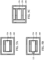
- FIGs. 5A-5C are plan views of a semiconductor package structure, in accordance with some embodiments of the disclosure. It should be noted that FIGs. 5A-5C may be the plan view from the top of the semiconductor package structure 300, which is illustrated in FIG. 4 , and some components are omitted for brevity.
- the thermal interface material 120 surrounds the bonding layer 126, in accordance with some embodiments. Although not illustrated, the thermal interface material 120 may also surrounds the metal layer 124 (referring to FIG. 4 ) disposed below the bonding layer 126. The thermal interface material 120 may be disposed on the periphery of the molding layer 108.
- the thermal interface material 120 is spaced apart from the metal layer 124 and the bonding layer 126 by a gap to prevent the issues caused by the different coefficients of thermal expansion (CTE) of the thermal interface material 120 and the metal layer 124 and the bonding layer 126. As a result, the reliability of the semiconductor package structure can be improved.
- CTE coefficients of thermal expansion
- the thermal interface material 120 partially surrounds the bonding layer 126, in accordance with some embodiments.
- the thermal interface material 120 may also partially surrounds the metal layer 124 disposed below the bonding layer 126.
- the thermal interface material 120 is cut off by a gap 132, in some embodiments.
- the gap 132 may release the gas generated during the manufacturing process. Therefore, the reliability of the semiconductor package structure can be further improved.
- the thermal interface material 120 may be cut off by a plurality of gaps, as illustrated in FIG. 5C .
- the thermal interface material 120 may include a plurality of separate sections.
- the thermal interface material 120 instead of being cut off by gaps, has a notch (not illustrated) to release the gas. In other embodiments, the thermal interface material 120 is cut off by one or more gaps 132 and/or has one or more notches.
- FIG. 6 is a cross-sectional view of a semiconductor package structure 400, in accordance with some other embodiments of the disclosure.
- the semiconductor package structure 400 may include the same or similar components as that of the semiconductor package structure 200, and for the sake of simplicity, those components will not be discussed in detail again.
- the following embodiments further provides another heatsink disposed below the substrate 102 to further improve the heat-dissipation efficiency.
- the semiconductor package structure 400 includes the heatsink 122 and a heatsink 130 disposed on opposite sides of the substrate 102, in accordance with some embodiments.
- the heatsink 130 may be bonded onto the substrate 102 through a bonding layer 128.
- the bonding layer 128 may include a metal or solder material.
- the bonding layer 128 may be lead, tin, indium, silver, copper, the like, an alloy thereof, or a combination thereof.
- the present disclosure may include more than two heatsinks as needed.
- the heatsink 130 is bonded before bonding the heatsink 122.
- the bonding layer 128 will melt and cause the heatsink 130 to fall off during the process such as reflow.
- the bonding layer 126 having a melting point lower than the bonding layer 128 can prevent this issue, in accordance with some embodiments.
- the bonding layer 126 may include SnBi, SnBiAg, the like, or a combination thereof.
- the composition of the bonding layers may be adjusted based on the process sequence. For example, if the heatsink 122 is bonded before bonding the heatsink 130, the bonding layer 128 used for bonding the heatsink 130 may have a melting point lower than the bonding layer 126 used for bonding the heatsink 122. Therefore, the reliability of the semiconductor package structure 400 can be improved.
- the present disclosure provides a semiconductor package structure including the bonding layer and the thermal interface material, which are used to bond the heatsink onto the substrate, so that the heat-dissipation efficiency can be improved without increasing the stress. Therefore, thermal performance, manufacturability and the reliability of the semiconductor package structure can be enhanced at the same time.
- the thermal interface material and the bonding layer are spaced apart by a gap to prevent the CTE mismatch.
- the thermal interface material cut off by one or more gaps and/or the thermal interface material having one or more notches can release the gas generated during the manufacturing process.
- the semiconductor package structure has a plurality of heatsinks on opposite sides to further improve the heat-dissipation efficiency.
- the bonding layer for the former may has a melting point lower than the bonding layer for latter. Therefore, the risk of the heatsink falling off during the process can be reduced, thereby improving the reliability of the semiconductor package structure.
- the semiconductor package structures in accordance with some embodiments of the disclosure can be used to form a three-dimensional (3D) package, a 2.5D package, a fan-out package, or another suitable package.
Landscapes
- Cooling Or The Like Of Semiconductors Or Solid State Devices (AREA)
- Structures Or Materials For Encapsulating Or Coating Semiconductor Devices Or Solid State Devices (AREA)
Abstract
Description
- This application claims the benefit of
U.S. Provisional Application No. 62/861,379, filed on June 14, 2019 U.S. Provisional Application No. 62/985,371, filed on March 5, 2020 - The present invention relates to a semiconductor package structure, and in particular to a semiconductor package structure having a thermal interface material.
- A semiconductor package structure can not only provide a semiconductor die with protection from environmental contaminants, but it can also provide an electrical connection between the semiconductor die packaged therein and a substrate, such as a printed circuit board (PCB).
- Heat is generated during the operation of the semiconductor die. If the heat is not adequately removed, the increased temperatures may result in damage to the semiconductor components, and may cause thermal stress and warpage of the semiconductor package structure.
- A heat dissipation device is needed to be disposed in the semiconductor package structure. A heatsink is commonly used to transfer the heat away. A thermal interface material is interposed between the semiconductor die and the heatsink to facilitate heat transfer from the semiconductor die to the heatsink. However, while existing heat dissipation devices in the semiconductor package structure generally meet requirements, they are not satisfactory in every respect, and further improvements are needed to improve the heat-dissipation efficiency.
- Semiconductor package structures are provided. An exemplary embodiment of a semiconductor package structure includes a substrate, a semiconductor die, a molding material, a first bonding layer, and a thermal interface material. The semiconductor die is disposed over the substrate. The molding material surrounds the semiconductor die. The first bonding layer is disposed over the semiconductor die. The thermal interface material is disposed over the molding material.
- Another exemplary embodiment of a semiconductor package structure includes a substrate, a semiconductor die, a molding material, a metal layer, a bonding layer, and a thermal interface material. The semiconductor die is disposed over the substrate. The molding material surrounds the semiconductor die. The metal layer is disposed over the semiconductor die. The bonding layer is disposed over the metal layer. The thermal interface material is disposed over the molding material.
- Yet another exemplary embodiment of a semiconductor package structure includes a substrate, a semiconductor die, a bonding layer, a molding material, and a thermal interface material. The semiconductor die is disposed over the substrate. The bonding layer is disposed over the semiconductor die. The molding material surrounds the semiconductor die. The thermal interface material is disposed over the molding material and partially surrounds the bonding layer, wherein the thermal interface material and the bonding layer are spaced apart by a gap.
- A detailed description is given in the following embodiments with reference to the accompanying drawings.
- The present invention can be more fully understood by reading the subsequent detailed description and examples with references made to the accompanying drawings, wherein:
-
FIG. 1 is a cross-sectional view of a semiconductor package structure, in accordance with some embodiments of the disclosure; -
FIG. 2 is a cross-sectional view of a semiconductor package structure, in accordance with some other embodiments of the disclosure; -
FIGs. 3A-3B are plan views of a semiconductor package structure, in accordance with some embodiments of the disclosure; -
FIG. 4 is a cross-sectional view of a semiconductor package structure, in accordance with some other embodiments of the disclosure; -
FIGs. 5A-5C are plan views of a semiconductor package structure, in accordance with some embodiments of the disclosure; and -
FIG. 6 is a cross-sectional view of a semiconductor package structure, in accordance with some other embodiments of the disclosure. - The following description is of the best-contemplated mode of carrying out the invention. This description is made for the purpose of illustrating the general principles of the invention and should not be taken in a limiting sense. The scope of the invention is determined by reference to the appended claims.
- The present invention is described with respect to particular embodiments and with reference to certain drawings, but the invention is not limited thereto and is only limited by the claims. The drawings described are only schematic and are non-limiting. In the drawings, the size of some of the elements may be exaggerated for illustrative purposes and not drawn to scale. The dimensions and the relative dimensions do not correspond to actual dimensions in the practice of the invention.
-
FIG. 1 is a cross-sectional view of asemiconductor package structure 100, in accordance with some embodiments of the disclosure. Additional features can be added to thesemiconductor package structure 100. Some of the features described below can be replaced or eliminated for different embodiments. To simplify the diagram, only a portion of thesemiconductor package structure 100 is depicted inFIG. 1 . - As illustrated in
FIG. 1 , asubstrate 102 is provided, in accordance with some embodiments. Thesubstrate 102 may be a coreless/core substrate or a printed circuit board (PCB). Thesubstrate 102 may be formed of polypropylene (PP), Polyimide, BT/Epoxy, Prepreg, ABF, ceramic material or other suitable material. Any desired semiconductor element may be formed in and on thesubstrate 102. However, in order to simplify the Figures, only theflat substrate 102 is illustrated. - The
semiconductor package structure 100 may include a semiconductor die 106 disposed over thesubstrate 102. For the sake of simplicity,FIG. 1 only shows one semiconductor die 106, in accordance with some embodiments. In some embodiments, multiple semiconductor dies 106 could be disposed over thesubstrate 102 and arranged side-by-side. In some embodiments, the semiconductor die 106 is an active device. For example, the semiconductor die 106 is a system-on-chip (SOC) die that may include a microcontroller (MCU), a microprocessor (MPU), a power management integrated circuit (PMIC), a global positioning system (GPS) device, or a radio frequency (RF) device, the like, or any combination thereof. Alternatively, the semiconductor die 106 may be logic dies that may include a central processing unit (CPU), a graphics processing unit (GPU), a dynamic random access memory (DRAM) controller, the like, or any combination thereof. In some other embodiments, one or more passive devices are also bonded onto thesubstrate 102, such as resistors, capacitors, inductors, the like, or a combination thereof. - The
semiconductor package structure 100 includes amolding material 108 surrounding the semiconductor die 106, in accordance with some embodiments. Themolding material 108 may adjoin the sidewalls of the semiconductor die 106. Although the upper surface of the semiconductor die 106 is exposed as illustrated, the upper surface of the semiconductor die 106 may also be covered by themolding material 108. - In some embodiments, the
molding material 108 includes a nonconductive material such as an epoxy, a resin, a moldable polymer, or another suitable molding material. In some embodiments, themolding material 108 is applied as a substantial liquid, and then is cured through a chemical reaction. In some other embodiments, themolding material 108 is an ultraviolet (UV) or thermally cured polymer applied as a gel or malleable solid, and then is cured through a UV or thermal curing process. Themolding material 108 may be cured with a mold (not illustrated). - As illustrated in
FIG. 1 , the semiconductor die 106 and themolding material 108 are bonded onto thesubstrate 102 through aconductive element 104, in accordance with some embodiments. In some embodiments, theconductive element 104 includes conductive ball structures, conductive pillar structures, or conductive paste structures that are mounted on and electrically coupled to thesubstrate 102 in the bonding process. For example, theconductive element 104 may be land grid array (LGA), ball grid array (BGA), the like, or a combination thereof. - As illustrated in
FIG. 1 , thesemiconductor package structure 100 includes aheatsink 122 bonded onto the semiconductor die 106 through athermal interface material 120, in accordance with some embodiments. Theheatsink 122 may be made of Cu, Al, the like, or a combination thereof. Thethermal interface material 120 may include a polymer which is adhesive. For example, thethermal interface material 120 may be silicone adhesive, such as SE4450 epoxy from Dow-Corning. In other example, thethermal interface material 120 may also include ceramic material, such as crystalline oxide, nitride or carbide material. - However, side effects may occur when only using the
thermal interface material 120 to connect theheatsink 122 and the semiconductor die 106, in some embodiments. Typically, thethermal interface material 120 with high viscosity has low thermal conductivity. Therefore, thethermal interface material 120 may be the thermal bottleneck between the semiconductor die 106 and theheatsink 122. Therefore, the present disclosure provides another embodiment to solve the above problem. -
FIG. 2 is a cross-sectional view of asemiconductor package structure 200, in accordance with some other embodiments of the disclosure. It should be noted that thesemiconductor package structure 200 may include the same or similar components as that of thesemiconductor package structure 100, which is illustrated inFIG. 1 , and for the sake of simplicity, those components will not be discussed in detail again. In comparison with the embodiment ofFIG. 1 where theheatsink 122 and the semiconductor die 106 are bonded only through thethermal interface material 120, the following embodiments will replace a portion of thethermal interface material 120 with a bonding layer to improve the heat-dissipation efficiency. - Additional features can be added to the
semiconductor package structure 200. Some of the features described below can be replaced or eliminated for different embodiments. To simplify the diagram, only a portion of thesemiconductor package structure 200 is depicted inFIG. 2 . - As illustrated in
FIG. 2 , ametal layer 124 is disposed on the semiconductor die 106 to provide a surface for the bonding layer to form thereon, in accordance with some embodiments. Themetal layer 124 may be formed on the semiconductor die 106 through a backside metallization (BSM) technology. In some embodiments, themetal layer 124 is formed by chemical vapor deposition, sputter deposition, plating, the like, or a combination thereof. Themetal layer 124 may include gold, silver, chromium, titanium, tungsten, vanadium, nickel, the like, an alloy thereof, or a combination thereof. Themetal layer 124 may also include Stainless Steel (SUS) material. Themetal layer 124 may be a single layer or multiple layers. - Although the semiconductor die 106 is coplanar with the
molding material 108 as illustrated, the present disclosure is not limit thereto. For example, in some embodiments, themolding material 108 is formed after the formation of themetal layer 124, and themolding material 108 also surrounds themetal layer 124. In these embodiments, themolding material 108 is coplanar with themetal layer 124. - As illustrated in
FIG. 2 , abonding layer 126 is disposed on themetal layer 124, in accordance with some embodiments. Thebonding layer 126 may include a metal or solder material. For example, thebonding layer 126 may be lead, tin, indium, silver, copper, the like, an alloy thereof, or a combination thereof. Since thebonding layer 126 has better thermal conductivity than thethermal interface material 120, such as 10 times thermal conductivity than thethermal interface material 120, the heat-dissipation efficiency can be improved by disposing thebonding layer 126. - However, if only the
bonding layer 126 is used to bond theheatsink 122 to the semiconductor die 106, the stress may be high. In this case, thebonding layer 126 may fragile during the sequential process, such as surface mount technology (SMT), thereby causing yield loss. Therefore, thesemiconductor package structure 200 according to the present disclosure includes both of thethermal interface material 120 and thebonding layer 126, thereby improving the heat-dissipation efficiency without increasing stress, which is preferred for high-power applications. As a result, thermal performance, manufacturability and the reliability can be enhanced at the same time. - As illustrated in
FIG. 2 , theheatsink 122 is connected to themolding material 108 through thethermal interface material 120, and connected to the semiconductor die 106 through themetal layer 124 and thebonding layer 126, in accordance with some embodiments. Thethermal interface material 120 may be disposed on the edge of themolding layer 108. In particular, the sidewall of thethermal interface material 120 may be aligned with the sidewall of themolding layer 108. - In some embodiments, the
thermal interface material 120 is spaced apart from themetal layer 124 and thebonding layer 126 by a gap to prevent the issues caused by the different coefficients of thermal expansion (CTE) of thethermal interface material 120 and themetal layer 124 and thebonding layer 126. As a result, the reliability of the semiconductor package structure can be improved. - In some embodiments, the
thermal interface material 120 is thicker than themetal layer 124 and is thicker than thebonding layer 126 to provide a planar surface for bonding theheatsink 122 thereon. Alternatively, as described above, in some other embodiments, themolding material 108 is coplanar with themetal layer 124. In these embodiments, the thickness of thethermal interface material 120 may be substantially equal to the thickness of thebonding layer 126 to provide a planar surface for bonding theheatsink 122 thereon. -
FIGs. 3A-3B are plan views of a semiconductor package structure, in accordance with some embodiments of the disclosure. It should be noted thatFIGs. 3A-3B may be the plan view from the top of thesemiconductor package structure 200, which is illustrated inFIG. 2 , and some components are omitted for brevity. - As illustrated in
FIG. 3A , thethermal interface material 120 surrounds thebonding layer 126, in accordance with some embodiments. Although not illustrated, thethermal interface material 120 may also surrounds the metal layer 124 (referring toFIG. 2 ) disposed below thebonding layer 126. Thethermal interface material 120 may be disposed on the edge of themolding layer 108. In particular, the sidewall of thethermal interface material 120 may be aligned with the sidewall of themolding layer 108. - In some embodiments, the
thermal interface material 120 is spaced apart from themetal layer 124 and thebonding layer 126 by a gap to prevent the issues caused by the different coefficients of thermal expansion (CTE) of thethermal interface material 120 and themetal layer 124 and thebonding layer 126. As a result, the reliability of the semiconductor package structure can be improved. - As illustrated in
FIG. 3B , thethermal interface material 120 partially surrounds thebonding layer 126, in accordance with some embodiments. Although not illustrated, thethermal interface material 120 may also partially surrounds themetal layer 124 disposed below thebonding layer 126. In other words, thethermal interface material 120 is cut off by agap 132, in some embodiments. Thegap 132 may release the gas generated during the manufacturing process. Therefore, the reliability of the semiconductor package structure can be further improved. - Although only one
gap 132 is illustrated inFIG. 3B , the present disclosure is not limited thereto. For example, thethermal interface material 120 may be cut off by a plurality of gaps. In particular, thethermal interface material 120 may include a plurality of separate sections. - In some embodiments, instead of being cut off by gaps, the
thermal interface material 120 has a notch (not illustrated) to release the gas. In other embodiments, thethermal interface material 120 is cut off by one ormore gaps 132 and/or has one or more notches. -
FIG. 4 is a cross-sectional view of asemiconductor package structure 300, in accordance with some other embodiments of the disclosure. It should be noted that thesemiconductor package structure 300 may include the same or similar components as that of thesemiconductor package structure 200, which is illustrated inFIG. 2 , and for the sake of simplicity, those components will not be discussed in detail again. In comparison with the embodiment ofFIG. 2 where thethermal interface material 120 is disposed on the edge of themolding layer 108, thethermal interface material 120 is disposed on the periphery of themolding layer 108. In particular, the sidewalls of thethermal interface material 120 may be inside the sidewalls of themolding layer 108. -
FIGs. 5A-5C are plan views of a semiconductor package structure, in accordance with some embodiments of the disclosure. It should be noted thatFIGs. 5A-5C may be the plan view from the top of thesemiconductor package structure 300, which is illustrated inFIG. 4 , and some components are omitted for brevity. - As illustrated in
FIG. 5A , thethermal interface material 120 surrounds thebonding layer 126, in accordance with some embodiments. Although not illustrated, thethermal interface material 120 may also surrounds the metal layer 124 (referring toFIG. 4 ) disposed below thebonding layer 126. Thethermal interface material 120 may be disposed on the periphery of themolding layer 108. - In some embodiments, the
thermal interface material 120 is spaced apart from themetal layer 124 and thebonding layer 126 by a gap to prevent the issues caused by the different coefficients of thermal expansion (CTE) of thethermal interface material 120 and themetal layer 124 and thebonding layer 126. As a result, the reliability of the semiconductor package structure can be improved. - As illustrated in
FIG. 5B , thethermal interface material 120 partially surrounds thebonding layer 126, in accordance with some embodiments. Although not illustrated, thethermal interface material 120 may also partially surrounds themetal layer 124 disposed below thebonding layer 126. In other words, thethermal interface material 120 is cut off by agap 132, in some embodiments. Thegap 132 may release the gas generated during the manufacturing process. Therefore, the reliability of the semiconductor package structure can be further improved. - Although only one
gap 132 is illustrated inFIG. 5B , the present disclosure is not limited thereto. For example, thethermal interface material 120 may be cut off by a plurality of gaps, as illustrated inFIG. 5C . In particular, thethermal interface material 120 may include a plurality of separate sections. - In some embodiments, instead of being cut off by gaps, the
thermal interface material 120 has a notch (not illustrated) to release the gas. In other embodiments, thethermal interface material 120 is cut off by one ormore gaps 132 and/or has one or more notches. -
FIG. 6 is a cross-sectional view of asemiconductor package structure 400, in accordance with some other embodiments of the disclosure. It should be noted that thesemiconductor package structure 400 may include the same or similar components as that of thesemiconductor package structure 200, and for the sake of simplicity, those components will not be discussed in detail again. In comparison with the embodiment ofFIG. 2 where theheatsink 122 is disposed over thesubstrate 102, the following embodiments further provides another heatsink disposed below thesubstrate 102 to further improve the heat-dissipation efficiency. - As illustrated in
FIG. 6 , thesemiconductor package structure 400 includes theheatsink 122 and aheatsink 130 disposed on opposite sides of thesubstrate 102, in accordance with some embodiments. Theheatsink 130 may be bonded onto thesubstrate 102 through abonding layer 128. Thebonding layer 128 may include a metal or solder material. For example, thebonding layer 128 may be lead, tin, indium, silver, copper, the like, an alloy thereof, or a combination thereof. Although only two heatsinks (theheatsink 122 and heatsink 130) are illustrated, the present disclosure may include more than two heatsinks as needed. - In an embodiment, the
heatsink 130 is bonded before bonding theheatsink 122. In this embodiment, if the temperature of bonding theheatsink 122 is higher than or substantially equal to the melting point of thebonding layer 128, thebonding layer 128 will melt and cause theheatsink 130 to fall off during the process such as reflow. In this regard, thebonding layer 126 having a melting point lower than thebonding layer 128 can prevent this issue, in accordance with some embodiments. For example, thebonding layer 126 may include SnBi, SnBiAg, the like, or a combination thereof. - Similarly, the composition of the bonding layers may be adjusted based on the process sequence. For example, if the
heatsink 122 is bonded before bonding theheatsink 130, thebonding layer 128 used for bonding theheatsink 130 may have a melting point lower than thebonding layer 126 used for bonding theheatsink 122. Therefore, the reliability of thesemiconductor package structure 400 can be improved. - In summary, the present disclosure provides a semiconductor package structure including the bonding layer and the thermal interface material, which are used to bond the heatsink onto the substrate, so that the heat-dissipation efficiency can be improved without increasing the stress. Therefore, thermal performance, manufacturability and the reliability of the semiconductor package structure can be enhanced at the same time.
- Furthermore, according to some embodiments, the thermal interface material and the bonding layer are spaced apart by a gap to prevent the CTE mismatch. In addition, according to some embodiments, the thermal interface material cut off by one or more gaps and/or the thermal interface material having one or more notches can release the gas generated during the manufacturing process.
- Moreover, in some embodiments, the semiconductor package structure has a plurality of heatsinks on opposite sides to further improve the heat-dissipation efficiency. In the embodiment where the heatsink is bonded onto the semiconductor die after the other heatsink is bonded onto the substrate, the bonding layer for the former may has a melting point lower than the bonding layer for latter. Therefore, the risk of the heatsink falling off during the process can be reduced, thereby improving the reliability of the semiconductor package structure.
- Many variations and/or modifications can be made to embodiments of the disclosure. The semiconductor package structures in accordance with some embodiments of the disclosure can be used to form a three-dimensional (3D) package, a 2.5D package, a fan-out package, or another suitable package.
- While the invention has been described by way of example and in terms of the preferred embodiments, it is to be understood that the invention is not limited to the disclosed embodiments. On the contrary, it is intended to cover various modifications and similar arrangements (as would be apparent to those skilled in the art). Therefore, the scope of the appended claims should be accorded the broadest interpretation so as to encompass all such modifications and similar arrangements.
Claims (15)
- A semiconductor package structure, comprising:a substrate;a semiconductor die disposed over the substrate;a molding material surrounding the semiconductor die;a first bonding layer disposed over the semiconductor die; anda thermal interface material disposed over the molding material.
- The semiconductor package structure as claimed in claim 1, further comprising a heatsink disposed over the bonding layer.
- The semiconductor package structure as claimed in claim 2, wherein the thermal interface material connects the molding material and the heatsink.
- The semiconductor package structure as claimed in one of the preceding claims, wherein the thermal interface material is adhesive.
- The semiconductor package structure as claimed in one of the preceding claims, wherein the thermal interface material surrounds the first bonding layer.
- The semiconductor package structure as claimed in one of the preceding claims, wherein the thermal interface material and the first bonding layer are spaced apart by a gap.
- The semiconductor package structure as claimed in one of the preceding claims, further comprising a metal layer disposed between the first bonding layer and the semiconductor die.
- The semiconductor package structure as claimed in claim 7, wherein the thermal interface material partially surrounds the metal layer and the bonding layer.
- The semiconductor package structure as claimed in claim 7 or 8, wherein the thermal interface material is spaced apart from the metal layer and the bonding layer by a gap; and/or
wherein the thermal interface material is thicker than the metal layer and thicker than the bonding layer. - The semiconductor package structure as claimed in one of the preceding claims, wherein the thermal interface material has a notch; and/or
wherein the thermal interface material is cut off by a gap; and/or.
wherein the thermal interface material is cut off by a plurality of gaps. - The semiconductor package structure as claimed in one of the preceding claims, further comprising a conductive element disposed between the semiconductor die and the substrate.
- The semiconductor package structure as claimed in one of the preceding claims, further comprising another heatsink disposed below the substrate, wherein the other heatsink is bonded onto the substrate through a second bonding layer.
- The semiconductor package structure as claimed in claim 12, wherein the first bonding layer has a melting point lower than the second bonding layer.
- The semiconductor package structure as claimed in one of the preceding claims, wherein the first bonding layer comprises SnBi, SnBiAg, or a combination thereof.
- The semiconductor package structure as claimed in one of the preceding claims, wherein a sidewall of the thermal interface material is aligned with a sidewall of the molding layer.
Applications Claiming Priority (3)
| Application Number | Priority Date | Filing Date | Title |
|---|---|---|---|
| US201962861379P | 2019-06-14 | 2019-06-14 | |
| US202062985371P | 2020-03-05 | 2020-03-05 | |
| US16/881,206 US11621211B2 (en) | 2019-06-14 | 2020-05-22 | Semiconductor package structure |
Publications (3)
| Publication Number | Publication Date |
|---|---|
| EP3751603A2 true EP3751603A2 (en) | 2020-12-16 |
| EP3751603A3 EP3751603A3 (en) | 2021-01-06 |
| EP3751603B1 EP3751603B1 (en) | 2024-10-09 |
Family
ID=71092245
Family Applications (1)
| Application Number | Title | Priority Date | Filing Date |
|---|---|---|---|
| EP20179156.3A Active EP3751603B1 (en) | 2019-06-14 | 2020-06-10 | Semiconductor package with a heat sink bonded to a semiconductor chip with a bonding layer and to a molding material with a thermal interface material |
Country Status (4)
| Country | Link |
|---|---|
| US (1) | US11621211B2 (en) |
| EP (1) | EP3751603B1 (en) |
| CN (1) | CN112086414A (en) |
| TW (1) | TWI721898B (en) |
Cited By (1)
| Publication number | Priority date | Publication date | Assignee | Title |
|---|---|---|---|---|
| FR3138733A1 (en) * | 2022-08-03 | 2024-02-09 | Stmicroelectronics (Grenoble 2) Sas | INTEGRATED CIRCUIT BOX |
Families Citing this family (3)
| Publication number | Priority date | Publication date | Assignee | Title |
|---|---|---|---|---|
| CN113745176A (en) * | 2021-07-14 | 2021-12-03 | 日月光半导体制造股份有限公司 | Semiconductor device |
| TWI872791B (en) * | 2023-11-07 | 2025-02-11 | 光寶科技股份有限公司 | Heat dissipation module |
| WO2026043692A1 (en) * | 2024-08-20 | 2026-02-26 | Kyocera International, Inc. | Electronics package with heterogenous heatsink |
Family Cites Families (36)
| Publication number | Priority date | Publication date | Assignee | Title |
|---|---|---|---|---|
| JP2914342B2 (en) | 1997-03-28 | 1999-06-28 | 日本電気株式会社 | Cooling structure of integrated circuit device |
| US5909056A (en) * | 1997-06-03 | 1999-06-01 | Lsi Logic Corporation | High performance heat spreader for flip chip packages |
| JP2000114413A (en) * | 1998-09-29 | 2000-04-21 | Sony Corp | Semiconductor device, manufacturing method thereof, and component mounting method |
| AU1348901A (en) * | 1999-10-28 | 2001-05-08 | P1 Diamond, Inc. | Improved diamond thermal management components |
| KR100446290B1 (en) * | 2001-11-03 | 2004-09-01 | 삼성전자주식회사 | Semiconductor package having dam and fabricating method the same |
| US6787899B2 (en) * | 2002-03-12 | 2004-09-07 | Intel Corporation | Electronic assemblies with solidified thixotropic thermal interface material |
| US6767765B2 (en) | 2002-03-27 | 2004-07-27 | Intel Corporation | Methods and apparatus for disposing a thermal interface material between a heat source and a heat dissipation device |
| US7408787B2 (en) * | 2003-07-30 | 2008-08-05 | Intel Corporation | Phase change thermal interface materials including polyester resin |
| US7312261B2 (en) * | 2004-05-11 | 2007-12-25 | International Business Machines Corporation | Thermal interface adhesive and rework |
| US7015577B2 (en) * | 2004-07-21 | 2006-03-21 | Advanced Semiconductor Engineering, Inc. | Flip chip package capable of measuring bond line thickness of thermal interface material |
| US7755184B2 (en) | 2004-12-03 | 2010-07-13 | Chris Macris | Liquid metal thermal interface material system |
| JP4155999B2 (en) | 2006-06-02 | 2008-09-24 | 株式会社ソニー・コンピュータエンタテインメント | Semiconductor device and manufacturing method of semiconductor device |
| JP4589269B2 (en) | 2006-06-16 | 2010-12-01 | ソニー株式会社 | Semiconductor device and manufacturing method thereof |
| US7999369B2 (en) | 2006-08-29 | 2011-08-16 | Denso Corporation | Power electronic package having two substrates with multiple semiconductor chips and electronic components |
| JP2010103244A (en) | 2008-10-22 | 2010-05-06 | Sony Corp | Semiconductor device, and method of manufacturing the same |
| US8232636B2 (en) * | 2010-01-26 | 2012-07-31 | International Business Machines Corporation | Reliability enhancement of metal thermal interface |
| CN102473653B (en) | 2010-02-01 | 2016-05-04 | 丰田自动车株式会社 | Manufacturing method of semiconductor device and semiconductor device |
| US8804331B2 (en) * | 2011-12-02 | 2014-08-12 | Ati Technologies Ulc | Portable computing device with thermal management |
| US9041192B2 (en) * | 2012-08-29 | 2015-05-26 | Broadcom Corporation | Hybrid thermal interface material for IC packages with integrated heat spreader |
| JP6130696B2 (en) * | 2013-03-26 | 2017-05-17 | 田中貴金属工業株式会社 | Semiconductor device |
| FR3011067B1 (en) * | 2013-09-23 | 2016-06-24 | Commissariat Energie Atomique | APPARATUS COMPRISING A FUNCTIONAL COMPONENT LIKELY TO BE OVERHEAD WHEN OPERATING AND A COMPONENT COOLING SYSTEM |
| US9287233B2 (en) | 2013-12-02 | 2016-03-15 | Taiwan Semiconductor Manufacturing Co., Ltd. | Adhesive pattern for advance package reliability improvement |
| US20150170989A1 (en) * | 2013-12-16 | 2015-06-18 | Hemanth K. Dhavaleswarapu | Three-dimensional (3d) integrated heat spreader for multichip packages |
| US10269682B2 (en) * | 2015-10-09 | 2019-04-23 | Taiwan Semiconductor Manufacturing Company, Ltd. | Cooling devices, packaged semiconductor devices, and methods of packaging semiconductor devices |
| US10049896B2 (en) * | 2015-12-09 | 2018-08-14 | International Business Machines Corporation | Lid attach optimization to limit electronic package warpage |
| EP3403279A4 (en) * | 2016-01-11 | 2019-09-11 | INTEL Corporation | HOUSING FOR MULTIPLE CHIPS COMPRISING SEVERAL THERMAL INTERFACE MATERIALS |
| US9918407B2 (en) * | 2016-08-02 | 2018-03-13 | Qualcomm Incorporated | Multi-layer heat dissipating device comprising heat storage capabilities, for an electronic device |
| CN106356341A (en) | 2016-08-31 | 2017-01-25 | 华为技术有限公司 | Semiconductor device and manufacture method |
| CN109148397B (en) | 2017-06-16 | 2023-02-28 | 日月光半导体制造股份有限公司 | Semiconductor device package |
| US10319609B2 (en) | 2017-06-21 | 2019-06-11 | International Business Machines Corporation | Adhesive-bonded thermal interface structures |
| US10483187B2 (en) * | 2017-06-30 | 2019-11-19 | Taiwan Semiconductor Manufacturing Company, Ltd. | Heat spreading device and method |
| US10431517B2 (en) * | 2017-08-25 | 2019-10-01 | Advanced Micro Devices, Inc. | Arrangement and thermal management of 3D stacked dies |
| US11817364B2 (en) | 2018-06-25 | 2023-11-14 | Intel Corporation | BGA STIM package architecture for high performance systems |
| DE102018216593A1 (en) | 2018-09-27 | 2020-04-02 | Robert Bosch Gmbh | Power semiconductor module |
| US11088109B2 (en) | 2018-11-21 | 2021-08-10 | Taiwan Semiconductor Manufacturing Co., Ltd. | Packages with multi-thermal interface materials and methods of fabricating the same |
| CN209029362U (en) * | 2018-11-23 | 2019-06-25 | 北京比特大陆科技有限公司 | Chip cooling structure, chip structure, circuit board and supercomputer equipment |
-
2020
- 2020-05-22 US US16/881,206 patent/US11621211B2/en active Active
- 2020-06-01 CN CN202010484230.5A patent/CN112086414A/en active Pending
- 2020-06-02 TW TW109118412A patent/TWI721898B/en active
- 2020-06-10 EP EP20179156.3A patent/EP3751603B1/en active Active
Cited By (1)
| Publication number | Priority date | Publication date | Assignee | Title |
|---|---|---|---|---|
| FR3138733A1 (en) * | 2022-08-03 | 2024-02-09 | Stmicroelectronics (Grenoble 2) Sas | INTEGRATED CIRCUIT BOX |
Also Published As
| Publication number | Publication date |
|---|---|
| EP3751603A3 (en) | 2021-01-06 |
| TW202101617A (en) | 2021-01-01 |
| US20200395267A1 (en) | 2020-12-17 |
| US11621211B2 (en) | 2023-04-04 |
| EP3751603B1 (en) | 2024-10-09 |
| CN112086414A (en) | 2020-12-15 |
| TWI721898B (en) | 2021-03-11 |
Similar Documents
| Publication | Publication Date | Title |
|---|---|---|
| US10510687B2 (en) | Packaging devices and methods for semiconductor devices | |
| EP2311084B1 (en) | Flip chip overmold package | |
| US7145226B2 (en) | Scalable microelectronic package using conductive risers | |
| US7138706B2 (en) | Semiconductor device and method for manufacturing the same | |
| US8008133B2 (en) | Chip package with channel stiffener frame | |
| US11621211B2 (en) | Semiconductor package structure | |
| US10032696B2 (en) | Chip package using interposer substrate with through-silicon vias | |
| US9922902B2 (en) | Semiconductor device and semiconductor package | |
| US20180151461A1 (en) | Stiffener for fan-out wafer level packaging and method of manufacturing | |
| US8519526B2 (en) | Semiconductor package and fabrication method thereof | |
| CN102132403B (en) | Molded ultra-thin semiconductor die package and system using same and method of manufacturing same | |
| US12550775B2 (en) | Semiconductor package with stiffener structure and method of manufacturing the same | |
| US20220102288A1 (en) | Semiconductor device and manufacturing method thereof | |
| JP2012015225A (en) | Semiconductor device | |
| KR102050130B1 (en) | Semiconductor package and a method of manufacturing the same | |
| US20150091152A1 (en) | External connection terminal, semiconductor package having external connection terminal and method of manufacturing the same | |
| JP2016219535A (en) | Electronic circuit device | |
| US9601407B2 (en) | System-in-package module and method for forming the same | |
| KR102340866B1 (en) | Semiconductor package and a method of manufacturing the same | |
| TWI774357B (en) | Semiconductor device with high heat dissipation effectiveness | |
| KR102365004B1 (en) | Semiconductor package and a method of manufacturing the same | |
| US20250140635A1 (en) | Electronic package and manufacturing method thereof | |
| TWM620388U (en) | Semiconductor device having high heat dissipation efficiency | |
| US20050082650A1 (en) | Integrated circuit packaging system | |
| JP2023092306A (en) | Semiconductor device |
Legal Events
| Date | Code | Title | Description |
|---|---|---|---|
| PUAI | Public reference made under article 153(3) epc to a published international application that has entered the european phase |
Free format text: ORIGINAL CODE: 0009012 |
|
| STAA | Information on the status of an ep patent application or granted ep patent |
Free format text: STATUS: THE APPLICATION HAS BEEN PUBLISHED |
|
| PUAL | Search report despatched |
Free format text: ORIGINAL CODE: 0009013 |
|
| AK | Designated contracting states |
Kind code of ref document: A2 Designated state(s): AL AT BE BG CH CY CZ DE DK EE ES FI FR GB GR HR HU IE IS IT LI LT LU LV MC MK MT NL NO PL PT RO RS SE SI SK SM TR |
|
| AX | Request for extension of the european patent |
Extension state: BA ME |
|
| AK | Designated contracting states |
Kind code of ref document: A3 Designated state(s): AL AT BE BG CH CY CZ DE DK EE ES FI FR GB GR HR HU IE IS IT LI LT LU LV MC MK MT NL NO PL PT RO RS SE SI SK SM TR |
|
| AX | Request for extension of the european patent |
Extension state: BA ME |
|
| RIC1 | Information provided on ipc code assigned before grant |
Ipc: H01L 23/42 20060101ALI20201130BHEP Ipc: H01L 23/36 20060101ALI20201130BHEP Ipc: H01L 23/373 20060101ALI20201130BHEP Ipc: H01L 23/367 20060101AFI20201130BHEP Ipc: H01L 23/31 20060101ALI20201130BHEP |
|
| RIN1 | Information on inventor provided before grant (corrected) |
Inventor name: HSU, YAO-PANG Inventor name: HSU, CHIA-HAO Inventor name: CHEN, TAI-YU Inventor name: HSIEH, YA-JUI |
|
| STAA | Information on the status of an ep patent application or granted ep patent |
Free format text: STATUS: REQUEST FOR EXAMINATION WAS MADE |
|
| 17P | Request for examination filed |
Effective date: 20210629 |
|
| RBV | Designated contracting states (corrected) |
Designated state(s): AL AT BE BG CH CY CZ DE DK EE ES FI FR GB GR HR HU IE IS IT LI LT LU LV MC MK MT NL NO PL PT RO RS SE SI SK SM TR |
|
| STAA | Information on the status of an ep patent application or granted ep patent |
Free format text: STATUS: EXAMINATION IS IN PROGRESS |
|
| 17Q | First examination report despatched |
Effective date: 20230208 |
|
| P01 | Opt-out of the competence of the unified patent court (upc) registered |
Effective date: 20230607 |
|
| GRAP | Despatch of communication of intention to grant a patent |
Free format text: ORIGINAL CODE: EPIDOSNIGR1 |
|
| STAA | Information on the status of an ep patent application or granted ep patent |
Free format text: STATUS: GRANT OF PATENT IS INTENDED |
|
| INTG | Intention to grant announced |
Effective date: 20240430 |
|
| GRAS | Grant fee paid |
Free format text: ORIGINAL CODE: EPIDOSNIGR3 |
|
| GRAA | (expected) grant |
Free format text: ORIGINAL CODE: 0009210 |
|
| STAA | Information on the status of an ep patent application or granted ep patent |
Free format text: STATUS: THE PATENT HAS BEEN GRANTED |
|
| AK | Designated contracting states |
Kind code of ref document: B1 Designated state(s): AL AT BE BG CH CY CZ DE DK EE ES FI FR GB GR HR HU IE IS IT LI LT LU LV MC MK MT NL NO PL PT RO RS SE SI SK SM TR |
|
| REG | Reference to a national code |
Ref country code: CH Ref legal event code: EP |
|
| REG | Reference to a national code |
Ref country code: DE Ref legal event code: R096 Ref document number: 602020038924 Country of ref document: DE |
|
| REG | Reference to a national code |
Ref country code: IE Ref legal event code: FG4D |
|
| REG | Reference to a national code |
Ref country code: LT Ref legal event code: MG9D |
|
| REG | Reference to a national code |
Ref country code: NL Ref legal event code: MP Effective date: 20241009 |
|
| REG | Reference to a national code |
Ref country code: AT Ref legal event code: MK05 Ref document number: 1731550 Country of ref document: AT Kind code of ref document: T Effective date: 20241009 |
|
| PG25 | Lapsed in a contracting state [announced via postgrant information from national office to epo] |
Ref country code: NL Free format text: LAPSE BECAUSE OF FAILURE TO SUBMIT A TRANSLATION OF THE DESCRIPTION OR TO PAY THE FEE WITHIN THE PRESCRIBED TIME-LIMIT Effective date: 20241009 |
|
| PG25 | Lapsed in a contracting state [announced via postgrant information from national office to epo] |
Ref country code: NL Free format text: LAPSE BECAUSE OF FAILURE TO SUBMIT A TRANSLATION OF THE DESCRIPTION OR TO PAY THE FEE WITHIN THE PRESCRIBED TIME-LIMIT Effective date: 20241009 |
|
| PG25 | Lapsed in a contracting state [announced via postgrant information from national office to epo] |
Ref country code: IS Free format text: LAPSE BECAUSE OF FAILURE TO SUBMIT A TRANSLATION OF THE DESCRIPTION OR TO PAY THE FEE WITHIN THE PRESCRIBED TIME-LIMIT Effective date: 20250209 Ref country code: PT Free format text: LAPSE BECAUSE OF FAILURE TO SUBMIT A TRANSLATION OF THE DESCRIPTION OR TO PAY THE FEE WITHIN THE PRESCRIBED TIME-LIMIT Effective date: 20250210 Ref country code: HR Free format text: LAPSE BECAUSE OF FAILURE TO SUBMIT A TRANSLATION OF THE DESCRIPTION OR TO PAY THE FEE WITHIN THE PRESCRIBED TIME-LIMIT Effective date: 20241009 |
|
| PG25 | Lapsed in a contracting state [announced via postgrant information from national office to epo] |
Ref country code: FI Free format text: LAPSE BECAUSE OF FAILURE TO SUBMIT A TRANSLATION OF THE DESCRIPTION OR TO PAY THE FEE WITHIN THE PRESCRIBED TIME-LIMIT Effective date: 20241009 |
|
| PG25 | Lapsed in a contracting state [announced via postgrant information from national office to epo] |
Ref country code: BG Free format text: LAPSE BECAUSE OF FAILURE TO SUBMIT A TRANSLATION OF THE DESCRIPTION OR TO PAY THE FEE WITHIN THE PRESCRIBED TIME-LIMIT Effective date: 20241009 |
|
| PG25 | Lapsed in a contracting state [announced via postgrant information from national office to epo] |
Ref country code: ES Free format text: LAPSE BECAUSE OF FAILURE TO SUBMIT A TRANSLATION OF THE DESCRIPTION OR TO PAY THE FEE WITHIN THE PRESCRIBED TIME-LIMIT Effective date: 20241009 |
|
| PG25 | Lapsed in a contracting state [announced via postgrant information from national office to epo] |
Ref country code: NO Free format text: LAPSE BECAUSE OF FAILURE TO SUBMIT A TRANSLATION OF THE DESCRIPTION OR TO PAY THE FEE WITHIN THE PRESCRIBED TIME-LIMIT Effective date: 20250109 |
|
| PG25 | Lapsed in a contracting state [announced via postgrant information from national office to epo] |
Ref country code: LV Free format text: LAPSE BECAUSE OF FAILURE TO SUBMIT A TRANSLATION OF THE DESCRIPTION OR TO PAY THE FEE WITHIN THE PRESCRIBED TIME-LIMIT Effective date: 20241009 Ref country code: AT Free format text: LAPSE BECAUSE OF FAILURE TO SUBMIT A TRANSLATION OF THE DESCRIPTION OR TO PAY THE FEE WITHIN THE PRESCRIBED TIME-LIMIT Effective date: 20241009 Ref country code: GR Free format text: LAPSE BECAUSE OF FAILURE TO SUBMIT A TRANSLATION OF THE DESCRIPTION OR TO PAY THE FEE WITHIN THE PRESCRIBED TIME-LIMIT Effective date: 20250110 |
|
| PG25 | Lapsed in a contracting state [announced via postgrant information from national office to epo] |
Ref country code: PL Free format text: LAPSE BECAUSE OF FAILURE TO SUBMIT A TRANSLATION OF THE DESCRIPTION OR TO PAY THE FEE WITHIN THE PRESCRIBED TIME-LIMIT Effective date: 20241009 |
|
| PG25 | Lapsed in a contracting state [announced via postgrant information from national office to epo] |
Ref country code: RS Free format text: LAPSE BECAUSE OF FAILURE TO SUBMIT A TRANSLATION OF THE DESCRIPTION OR TO PAY THE FEE WITHIN THE PRESCRIBED TIME-LIMIT Effective date: 20250109 |
|
| PG25 | Lapsed in a contracting state [announced via postgrant information from national office to epo] |
Ref country code: SM Free format text: LAPSE BECAUSE OF FAILURE TO SUBMIT A TRANSLATION OF THE DESCRIPTION OR TO PAY THE FEE WITHIN THE PRESCRIBED TIME-LIMIT Effective date: 20241009 |
|
| PGFP | Annual fee paid to national office [announced via postgrant information from national office to epo] |
Ref country code: DE Payment date: 20250429 Year of fee payment: 6 |
|
| PG25 | Lapsed in a contracting state [announced via postgrant information from national office to epo] |
Ref country code: DK Free format text: LAPSE BECAUSE OF FAILURE TO SUBMIT A TRANSLATION OF THE DESCRIPTION OR TO PAY THE FEE WITHIN THE PRESCRIBED TIME-LIMIT Effective date: 20241009 |
|
| PGFP | Annual fee paid to national office [announced via postgrant information from national office to epo] |
Ref country code: GB Payment date: 20250425 Year of fee payment: 6 |
|
| REG | Reference to a national code |
Ref country code: DE Ref legal event code: R097 Ref document number: 602020038924 Country of ref document: DE |
|
| PG25 | Lapsed in a contracting state [announced via postgrant information from national office to epo] |
Ref country code: EE Free format text: LAPSE BECAUSE OF FAILURE TO SUBMIT A TRANSLATION OF THE DESCRIPTION OR TO PAY THE FEE WITHIN THE PRESCRIBED TIME-LIMIT Effective date: 20241009 |
|
| PGFP | Annual fee paid to national office [announced via postgrant information from national office to epo] |
Ref country code: FR Payment date: 20250508 Year of fee payment: 6 |
|
| PG25 | Lapsed in a contracting state [announced via postgrant information from national office to epo] |
Ref country code: RO Free format text: LAPSE BECAUSE OF FAILURE TO SUBMIT A TRANSLATION OF THE DESCRIPTION OR TO PAY THE FEE WITHIN THE PRESCRIBED TIME-LIMIT Effective date: 20241009 |
|
| PG25 | Lapsed in a contracting state [announced via postgrant information from national office to epo] |
Ref country code: SK Free format text: LAPSE BECAUSE OF FAILURE TO SUBMIT A TRANSLATION OF THE DESCRIPTION OR TO PAY THE FEE WITHIN THE PRESCRIBED TIME-LIMIT Effective date: 20241009 |
|
| PG25 | Lapsed in a contracting state [announced via postgrant information from national office to epo] |
Ref country code: CZ Free format text: LAPSE BECAUSE OF FAILURE TO SUBMIT A TRANSLATION OF THE DESCRIPTION OR TO PAY THE FEE WITHIN THE PRESCRIBED TIME-LIMIT Effective date: 20241009 |
|
| PG25 | Lapsed in a contracting state [announced via postgrant information from national office to epo] |
Ref country code: IT Free format text: LAPSE BECAUSE OF FAILURE TO SUBMIT A TRANSLATION OF THE DESCRIPTION OR TO PAY THE FEE WITHIN THE PRESCRIBED TIME-LIMIT Effective date: 20241009 |
|
| PLBE | No opposition filed within time limit |
Free format text: ORIGINAL CODE: 0009261 |
|
| STAA | Information on the status of an ep patent application or granted ep patent |
Free format text: STATUS: NO OPPOSITION FILED WITHIN TIME LIMIT |
|
| PG25 | Lapsed in a contracting state [announced via postgrant information from national office to epo] |
Ref country code: SE Free format text: LAPSE BECAUSE OF FAILURE TO SUBMIT A TRANSLATION OF THE DESCRIPTION OR TO PAY THE FEE WITHIN THE PRESCRIBED TIME-LIMIT Effective date: 20241009 |
|
| 26N | No opposition filed |
Effective date: 20250710 |
|
| REG | Reference to a national code |
Ref country code: DE Ref legal event code: R079 Ref document number: 602020038924 Country of ref document: DE Free format text: PREVIOUS MAIN CLASS: H01L0023367000 Ipc: H10W0040220000 |
|
| REG | Reference to a national code |
Ref country code: CH Ref legal event code: H13 Free format text: ST27 STATUS EVENT CODE: U-0-0-H10-H13 (AS PROVIDED BY THE NATIONAL OFFICE) Effective date: 20260127 |
|
| PG25 | Lapsed in a contracting state [announced via postgrant information from national office to epo] |
Ref country code: MC Free format text: LAPSE BECAUSE OF FAILURE TO SUBMIT A TRANSLATION OF THE DESCRIPTION OR TO PAY THE FEE WITHIN THE PRESCRIBED TIME-LIMIT Effective date: 20241009 |
|
| PG25 | Lapsed in a contracting state [announced via postgrant information from national office to epo] |
Ref country code: LU Free format text: LAPSE BECAUSE OF NON-PAYMENT OF DUE FEES Effective date: 20250610 |
|
| REG | Reference to a national code |
Ref country code: BE Ref legal event code: MM Effective date: 20250630 |
|
| PG25 | Lapsed in a contracting state [announced via postgrant information from national office to epo] |
Ref country code: IE Free format text: LAPSE BECAUSE OF NON-PAYMENT OF DUE FEES Effective date: 20250610 |
|
| PG25 | Lapsed in a contracting state [announced via postgrant information from national office to epo] |
Ref country code: BE Free format text: LAPSE BECAUSE OF NON-PAYMENT OF DUE FEES Effective date: 20250630 |
|
| PG25 | Lapsed in a contracting state [announced via postgrant information from national office to epo] |
Ref country code: CH Free format text: LAPSE BECAUSE OF NON-PAYMENT OF DUE FEES Effective date: 20250630 |