EP3751552B1 - Residual image elimination unit, control method therefor and liquid crystal display device - Google Patents
Residual image elimination unit, control method therefor and liquid crystal display device Download PDFInfo
- Publication number
- EP3751552B1 EP3751552B1 EP18852772.5A EP18852772A EP3751552B1 EP 3751552 B1 EP3751552 B1 EP 3751552B1 EP 18852772 A EP18852772 A EP 18852772A EP 3751552 B1 EP3751552 B1 EP 3751552B1
- Authority
- EP
- European Patent Office
- Prior art keywords
- circuit
- signal
- sub
- controlling
- voltage
- Prior art date
- Legal status (The legal status is an assumption and is not a legal conclusion. Google has not performed a legal analysis and makes no representation as to the accuracy of the status listed.)
- Active
Links
Images


Classifications
-
- G—PHYSICS
- G09—EDUCATION; CRYPTOGRAPHY; DISPLAY; ADVERTISING; SEALS
- G09G—ARRANGEMENTS OR CIRCUITS FOR CONTROL OF INDICATING DEVICES USING STATIC MEANS TO PRESENT VARIABLE INFORMATION
- G09G3/00—Control arrangements or circuits, of interest only in connection with visual indicators other than cathode-ray tubes
- G09G3/20—Control arrangements or circuits, of interest only in connection with visual indicators other than cathode-ray tubes for presentation of an assembly of a number of characters, e.g. a page, by composing the assembly by combination of individual elements arranged in a matrix no fixed position being assigned to or needed to be assigned to the individual characters or partial characters
- G09G3/34—Control arrangements or circuits, of interest only in connection with visual indicators other than cathode-ray tubes for presentation of an assembly of a number of characters, e.g. a page, by composing the assembly by combination of individual elements arranged in a matrix no fixed position being assigned to or needed to be assigned to the individual characters or partial characters by control of light from an independent source
- G09G3/36—Control arrangements or circuits, of interest only in connection with visual indicators other than cathode-ray tubes for presentation of an assembly of a number of characters, e.g. a page, by composing the assembly by combination of individual elements arranged in a matrix no fixed position being assigned to or needed to be assigned to the individual characters or partial characters by control of light from an independent source using liquid crystals
- G09G3/3611—Control of matrices with row and column drivers
- G09G3/3696—Generation of voltages supplied to electrode drivers
-
- G—PHYSICS
- G09—EDUCATION; CRYPTOGRAPHY; DISPLAY; ADVERTISING; SEALS
- G09G—ARRANGEMENTS OR CIRCUITS FOR CONTROL OF INDICATING DEVICES USING STATIC MEANS TO PRESENT VARIABLE INFORMATION
- G09G3/00—Control arrangements or circuits, of interest only in connection with visual indicators other than cathode-ray tubes
- G09G3/20—Control arrangements or circuits, of interest only in connection with visual indicators other than cathode-ray tubes for presentation of an assembly of a number of characters, e.g. a page, by composing the assembly by combination of individual elements arranged in a matrix no fixed position being assigned to or needed to be assigned to the individual characters or partial characters
- G09G3/34—Control arrangements or circuits, of interest only in connection with visual indicators other than cathode-ray tubes for presentation of an assembly of a number of characters, e.g. a page, by composing the assembly by combination of individual elements arranged in a matrix no fixed position being assigned to or needed to be assigned to the individual characters or partial characters by control of light from an independent source
- G09G3/36—Control arrangements or circuits, of interest only in connection with visual indicators other than cathode-ray tubes for presentation of an assembly of a number of characters, e.g. a page, by composing the assembly by combination of individual elements arranged in a matrix no fixed position being assigned to or needed to be assigned to the individual characters or partial characters by control of light from an independent source using liquid crystals
- G09G3/3611—Control of matrices with row and column drivers
- G09G3/3648—Control of matrices with row and column drivers using an active matrix
-
- G—PHYSICS
- G09—EDUCATION; CRYPTOGRAPHY; DISPLAY; ADVERTISING; SEALS
- G09G—ARRANGEMENTS OR CIRCUITS FOR CONTROL OF INDICATING DEVICES USING STATIC MEANS TO PRESENT VARIABLE INFORMATION
- G09G2300/00—Aspects of the constitution of display devices
- G09G2300/08—Active matrix structure, i.e. with use of active elements, inclusive of non-linear two terminal elements, in the pixels together with light emitting or modulating elements
- G09G2300/0809—Several active elements per pixel in active matrix panels
- G09G2300/0842—Several active elements per pixel in active matrix panels forming a memory circuit, e.g. a dynamic memory with one capacitor
-
- G—PHYSICS
- G09—EDUCATION; CRYPTOGRAPHY; DISPLAY; ADVERTISING; SEALS
- G09G—ARRANGEMENTS OR CIRCUITS FOR CONTROL OF INDICATING DEVICES USING STATIC MEANS TO PRESENT VARIABLE INFORMATION
- G09G2310/00—Command of the display device
- G09G2310/08—Details of timing specific for flat panels, other than clock recovery
-
- G—PHYSICS
- G09—EDUCATION; CRYPTOGRAPHY; DISPLAY; ADVERTISING; SEALS
- G09G—ARRANGEMENTS OR CIRCUITS FOR CONTROL OF INDICATING DEVICES USING STATIC MEANS TO PRESENT VARIABLE INFORMATION
- G09G2320/00—Control of display operating conditions
- G09G2320/02—Improving the quality of display appearance
- G09G2320/0257—Reduction of after-image effects
-
- G—PHYSICS
- G09—EDUCATION; CRYPTOGRAPHY; DISPLAY; ADVERTISING; SEALS
- G09G—ARRANGEMENTS OR CIRCUITS FOR CONTROL OF INDICATING DEVICES USING STATIC MEANS TO PRESENT VARIABLE INFORMATION
- G09G2330/00—Aspects of power supply; Aspects of display protection and defect management
- G09G2330/02—Details of power systems and of start or stop of display operation
- G09G2330/027—Arrangements or methods related to powering off a display
Definitions
- Embodiments of the present disclosure relate to the field of display technologies, and in particular, to an erasing unit for image sticking, a control method thereof and a liquid crystal display device.
- a liquid crystal display generally comprises an array substrate and a color filter substrate disposed opposite to each other and a liquid crystal layer disposed between the array substrate and the color filter substrate.
- liquid crystal molecules are controlled to deflect by applying voltages to pixel electrodes on the array substrate and common electrodes on the color filter substrate, respectively.
- capacitors in the LCD since there are capacitors in the LCD, some of charges may be stored on the pixel electrodes. If the charges stored in the LCD cannot be effectively released, it will result in image sticking when the LCD is turned off, i.e. an afterimage may appear. This may further cause a problem of shutdown afterimage.
- US 9 501 997 discloses a gate driver and a display device, wherein the gate driver comprises: a power-off voltage detection circuit and a power-off de-ghosting function circuit connected to the power-off voltage detection circuit.
- an erasing unit as defined in claim 1.
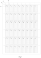
- an array substrate of the liquid crystal display device may include a gate line 01, a data line 02, a pixel electrode 03 disposed in an area defined by the gate line 01 and the data line 02, and a TFT 04 corresponding to each pixel electrode 03.
- the TFT 04 has a gate coupled to the gate line 01, a source coupled to the data line 02, and a drain coupled to the pixel electrode 03.
- gate scanning signals are sequentially inputted to each row of gate lines 01, so as to control turning on of each row of TFTs.
- the TFTs are turned on, corresponding data signals are loaded to the data lines 02, so as to write the data signals into the pixel electrode.
- a common voltage is applied to the common electrode on the color filter substrate in the liquid crystal display device, so as to form an electric field by the common voltage and the voltage of the pixel electrode, thereby controlling the deflecting of the liquid crystal molecules in the liquid crystal display device to realize an image display function.
- the liquid crystal display device can be supplied with a DC voltage, in other words, the voltage at the DC power supply terminal is used to supply power to the liquid crystal display device.
- the voltage at the DC power supply terminal can be obtained from an external DC power supply (typically 12V) through a step-down circuit.
- the external DC power supply can be a battery, a DC voltage which is converted from the voltage outputted from the battery by a direct current-direct current (DC-DC) conversion circuit, or a DC voltage which is converted from an AC voltage by an alternating current-direct current (AC-DC) conversion circuit, which will not be limited herein.
- DC-DC direct current-direct current
- AC-DC alternating current-direct current
- the triggering signal XAO controls a level conversion circuit to output a high-level signal Vgh (even if the level conversion circuit activates a XAO function), so as to control all thin film transistors (TFTs) in the array substrate to be turned on, thereby enabling the pixel electrodes to discharge the charges. This may help in mitigating the phenomenon of shutdown afterimage.
- the voltage of the high-level signal Vgh is also converted from the external DC power supply by a boosting circuit generally. Therefore, when the liquid crystal display device is turned off, that is, when the external DC power supply is powered down, the voltage of the external DC power supply drops, so that the voltage of the high-level signal Vgh also drops.
- the triggering signal XAO is required to be triggered when the voltage at the DC power supply terminal DVDD drops to a predetermined voltage value, and currently the voltage of the high-level signal Vgh also drops to a certain voltage, the voltage of the high-level signal Vgh which is applied on the TFT is insufficient to turn on the TFT completely in a case that the level conversion circuit actives the XAO function, thereby causing an insufficient charge release. This may result in a residual charge phenomenon, affecting the erasing effect for image sticking.
- Embodiments of the present disclosure provide an erasing unit for image sticking that can be applied to a liquid crystal display device.
- the charging and discharging circuit may achieve discharging when the liquid crystal display device is turned off, thereby ensuring that the voltage supplied to the gate of the TFT does not drop rapidly as the external DC power supply is powered down.
- the TFT can be enabled to be turned on completely and the turning-on time of the TFT can be extended. Accordingly, the charges can be completely released, thereby mitigating the residual charge phenomenon.
- the erasing unit for image sticking in the above liquid crystal display device may include a controlling circuit 20, a charging and discharging circuit 30 and an outputting circuit 40.
- the controlling circuit 20 may be configured to receive a first controlling signal, and output a second controlling signal and a third controlling signal in response to a voltage of the first controlling signal being less than or equal to a reference voltage.
- the charging and discharging circuit 30 may be configured to output a high-level voltage signal under a control of the second controlling signal.
- the outputting circuit 40 may be configured to output the high-level voltage signal to a gate of a thin film transistor in the liquid crystal display device 50 under a control of the third controlling signal.
- the first controlling signal can be derived by dividing the voltage at the DC power supply terminal.
- the voltage at the DC power supply terminal drops.
- the voltage of the first controlling signal is decreased to be less than or equal to the reference voltage, which may enable the controlling circuit to output the second controlling signal and the third controlling signal.
- the charging and discharging circuit discharges in response to receiving the second controlling signal, so as to provide the high-level voltage signal to the outputting circuit.
- the outputting circuit may transfer the high-level voltage signal outputted from the charging and discharging circuit to the gate of the TFT in the liquid crystal display device in response to receiving the third controlling signal, thereby controlling the TFT to be turned on.
- the voltage of the high-level voltage signal supplied to the outputting circuit is ensured not to drop rapidly as the external DC power supply is powered off, by discharging via the charging and discharging circuit when the liquid crystal display device is turned off.
- the TFT can be enabled to be turned on completely and the turning-on time of the TFT can be extended. Accordingly, the charges can be completely released, thereby mitigating the residual charge phenomenon and improving the erasing effect for image sticking.
- the charging and discharging circuit has a charging function and a discharging function.
- the voltage at the DC power supply terminal does not drop.
- the voltage of the first controlling signal is ensured not to be less than or equal to the reference voltage.
- the second controlling signal and the third controlling signal will not be generated by the controlling circuit, thereby preventing the charging and discharging circuit from discharging and preventing the operation of the outputting circuit from affecting the normal operation of the liquid crystal display device.
- the charging and discharging circuit can be charged when the liquid crystal display device is turned on and in the normal operation.
- another example of the erasing unit according to the embodiment of the present disclosure may further include a voltage dividing circuit 10 configured to divide a voltage at the DC power source terminal DVDD, so as to generate the first controlling signal.
- the controlling circuit 20 may comprise a comparing sub-circuit 21, a selecting sub-circuit 22, a timing sub-circuit 23, and an inverting sub-circuit 24.
- the comparing sub-circuit 21 is configured to receive the first controlling signal and a reference voltage signal VO, output a first selecting signal to the selecting sub-circuit 22 in response to the voltage of the first controlling signal being less than or equal to the reference voltage of the reference voltage signal VO; and output a second selecting signal to the selecting sub-circuit 22 in response to the voltage of the first controlling signal being greater than the reference voltage of the reference voltage signal VO.
- the selecting sub-circuit 22 is configured to output a timing controlling signal of a first level to the timing sub-circuit 23 under a control of the first selecting signal; and output a timing controlling signal of a second level to the timing sub-circuit 23 under a control of the second selecting signal.
- the timing sub-circuit 23 is configured to time a duration of the timing controlling signal of the first level, output a conduction controlling signal during a period of time with a duration being less than or equal to a threshold duration, and be paused under the control of the timing controlling signal of the second level.
- the inverting sub-circuit 24 is configured to invert the conduction controlling signal and output the inverted signal to the outputting circuit 40 as the third controlling signal.
- the requirement for erasing image sticking may be different depending on the size of the display panel in the liquid crystal display device and its application environment. For example, the larger the size of the display panel, the longer it takes to discharge. Therefore, in the specific implementation, a threshold for the duration can be set according to the discharging requirement of the liquid crystal display device. For example, when the liquid crystal display device is required to be discharged for a long time, the threshold duration can be set to a great value.
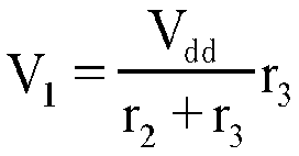
- the voltage dividing sub-circuit 10 comprises: a second resistor R2 and a third resistor R3.
- the second resistor R2 has a first terminal coupled to the DC power supply terminal DVDD, and a second terminal coupled to a first terminal of the third resistor R3 and the controlling circuit respectively and configured to output the first controlling signal.
- the third resistor R3 has a second electrode coupled to the ground terminal GND.
- the second electrode of the second resistor R2 is coupled to the comparing sub-circuit 21 in the controlling circuit.
- the comparing sub-circuit 21 may comprise a comparator OP, wherein the comparator OP has a negative phase inputting terminal coupled to the voltage dividing circuit 10 and configured to receive the first controlling signal, a positive phase inputting terminal configured to receive the reference voltage signal VO, and an outputting terminal coupled to the selecting sub-circuit 22 and configured to output the first selecting signal or the second selecting signal.
- the negative phase inputting terminal of the comparator OP is coupled to the second electrode of the second resistor R2 in the voltage dividing sub-circuit 10.
- the comparator OP can output the high-level signal when the voltage at its negative phase inputting terminal is less than or equal to the voltage at its positive phase inputting terminal; and output the low-level signal when the voltage at its negative phase inputting terminal is greater than the voltage at its positive phase inputting terminal.
- V o represents the reference voltage of the reference voltage signal.
- the comparator when V 1 ⁇ V o , the comparator outputs the high-level signal as the first selecting signal.
- V 1 >V o the comparator outputs the low-level signal as the second selecting signal.
- the voltage at the DC power supply terminal is relatively stable when the liquid crystal display device is turned on and in the normal operation.
- V 1 can be considered as a fixed voltage value, and V 1 >V o .
- V o the voltage at the DC power supply terminal will drop, and V 1 will drop accordingly.
- V 1 ⁇ V o will occur during the dropping.
- a voltage dropping speed of the DC power supply terminal should be determined according to the actual application environment, which is not limited herein. In practical applications, V o , r 2 , and r 3 may be also determined according to the above circumstances, and are not limited herein.
- the selecting sub-circuit 22 may comprise a second transistor M2 and a first resistor R1.
- the second transistor M2 has a controlling electrode coupled to the comparing sub-circuit 21 and configured to receive the first selecting signal or the second selecting signal, a first electrode coupled to the ground terminal GND, and a second electrode coupled to a first terminal of the first resistor R1 and the timing sub-circuit 23 respectively and configured to output the timing controlling signal.
- the first resistor R1 has a second electrode coupled to the reference signal terminal VREF.
- the controlling electrode of the second transistor M2 is coupled to the outputting terminal of the comparator OP in the comparing sub-circuit 21.
- the timing controlling signal may have a first level of a low-level and a second level of a high-level.
- the reference signal terminal will be conducted with the ground terminal.
- the voltage between the reference signal terminal and the ground terminal may be divided by the first resistor. Since the timing sub-circuit is coupled to the first electrode of the first resistor, the signal at the ground terminal is outputted to the timing sub-circuit 23 as the timing controlling signal of the first level. If the second transistor M2 is turned off under the control of the second selecting signal, the reference signal terminal is disconnected from the ground terminal. Since the timing sub-circuit is coupled to the first electrode of the first resistor, the signal at the reference signal terminal is outputted to the timing sub-circuit as the timing controlling signal of the second level.
- the second transistor may be a TFT or a metal oxide semiconductor (MOS) field effect transistor, which is not limited herein.
- the second transistor may have the controlling electrode implemented with a gate, the first electrode implemented with a source, and the second electrode implemented with a drain, or, conversely, the first electrode implemented with the drain, and the second electrode implemented with the source, which is not limited here.
- the reference signal terminal and the DC power supply terminal may be set as the same signal terminal.
- the second electrode of the first resistor R1 can be coupled to the DC power supply terminal DVDD.
- the signal at the DC power supply terminal DVDD can be outputted to the timing sub-circuit 23 as the timing controlling signal of the second level.
- the timing sub-circuit 23 may comprise a timer TM, wherein: the timer TM has a controlling terminal coupled to the selecting sub-circuit 22 and configured to receive the timing controlling signal, and an outputting terminal coupled to the inverting sub-circuit 24 and the charging and discharging circuit 30 and configured to output the conduction controlling signal.
- the controlling terminal of the timer TM is coupled to the first electrode of the first resistor R1 in the selecting sub-circuit 22.
- the timer may be triggered to start operation and timing under the control of the timing controlling signal of the first level, and output the conduction controlling signal during a period of time with a duration being less than or equal to the threshold duration.
- the timer may not be triggered under the control of the timing controlling signal having the second level, so as to be paused.
- the duration is greater than the threshold duration, the timer can also be paused, so as to avoid excessive power consumption due to the long duration of the timer.
- the timer can be a timer with a countdown function, and the duration of the timer can be a period from the start of the countdown to the countdown to a certain time.
- the duration of the countdown may be on the order of milliseconds, for example, 20 ms.
- the timer also needs to be powered on.
- the voltage derived by converting the voltage of the external DC power supply can be supplied to the timer. This may result in that the voltage supplied to the timer decreases as the voltage of the external DC power source decreases when the liquid crystal display device is turned off. Therefore, after completing the shutdown process of the liquid crystal display device, if the duration of the timer is still not greater than the threshold duration, the timer will also stop working. Moreover, when the liquid crystal display device is powered on again, the timer can be reset automatically or manually.
- the threshold duration can be set for the countdown duration of the timer.
- the specific structure of the timer can be understood by those of ordinary skill in the art, and details thereof are not described herein.
- the inversing sub-circuit 24 comprises an inverter N0, wherein: the inverter N0 has an inputting terminal coupled to the outputting terminal of the timing sub-circuit 23 and configured to receive the conduction controlling signal, and an outputting terminal coupled to the outputting circuit 40 and configured to output the third controlling signal.
- the inputting terminal of the inverter N0 is coupled to the outputting terminal of the timer TM in the timing sub-circuit 23.
- the inverter can enable the signal at its outputting terminal to have an opposite phase with the signal at its inputting terminal.
- the specific structure of the inverter can be understood by those skilled in the art and will not be described herein.
- the charging and discharging circuit 30 may comprise: a storage capacitor Cst and a first transistor M1.
- the storage capacitor Cst has a first electrode coupled to a high-level voltage signal terminal VGH and a first electrode of the first transistor M1, and a second electrode coupled to a ground terminal GND.
- the first transistor M1 has a gate coupled to the controlling sub-circuit and configured to receive the second controlling signal, and a second electrode coupled to the outputting circuit 40 and configured to output the high-level voltage signal.
- the gate of the first transistor M1 is coupled to the outputting terminal of the timer TM in the timing sub-circuit 23.
- the first transistor M1 may be turned on under the control of the second controlling signal, so as to connect the first electrode of the storage capacitor Cst to the outputting circuit.
- the first transistor may be a TFT or a MOS transistor, which is not limited herein.
- the first transistor have the controlling electrode implemented with the gate, the first electrode implemented with the source, and the second electrode implemented with the drain, and vice versa, which is not limited herein.
- the storage capacitor Cst has a charging and discharging function.
- the storage capacitor Cst can be implemented as a single capacitor or a capacitor bank.
- the size of the storage capacitor Cst can be determined according to the actual application environment, which is not limited herein.
- the voltage at the high-level voltage signal terminal can be obtained by converting the voltage of the external DC power supply via a boosting circuit.
- the storage capacitor Cst can be charged by inputting the signals at the high-level voltage signal terminal and the ground terminal, so as to store the voltage at the high-level voltage signal terminal.
- the first transistor M1 is turned on.
- the voltage at the high-level voltage signal terminal drops accordingly.
- the storage capacitor Cst can be discharged through the turned-on first transistor M1, so as to output the high-level voltage signal to the outputting circuit.
- the voltage of the high-level voltage signal outputted by the storage capacitor is approximately equal to the voltage at the high-level voltage signal terminal (in practice, the voltage outputted by the storage capacitor Cst may be slightly smaller than the voltage at the high-level voltage signal terminal).
- the discharging time of the storage capacitor Cst increases, the voltage of the outputted high-level voltage signal will gradually decrease.
- the storage capacitor Cst is capable of storing a voltage
- the speed at which the voltage resulted from the discharging of the storage capacitor decreases is smaller than the speed at which the voltage at the DC power source terminal decreases. Therefore, due to the discharging of the storage capacitor, the high-level voltage signal can be supplied to all the TFTs in the liquid crystal display device, enabling the TFT to be turned on completely.
- the speed at which the voltage outputted by the storage capacitor Cst decreases may be determined according to the size of the storage capacitor, and is not limited herein.
- the voltage at the high-level voltage signal terminal can be made smaller than the voltage at the DC power supply terminal, thereby reducing power consumption.
- the charging and discharging circuit 30 may further comprise: a first rectifier diode D1, a second rectifier diode D2, a third rectifier diode D3, and a fourth rectifier diode D4.
- the high-level voltage signal terminal VGH is coupled to the first electrode of the storage capacitor Cst via the first rectifier diode D1 and coupled to the second electrode of the storage capacitor Cst via the second rectifier diode D2.
- the ground terminal GND is coupled to the first electrode of the storage capacitor Cst via the third rectifier diode D3, and coupled to the second electrode of the storage capacitor Cst through the fourth rectifier diode D4.
- the first rectifier diode D1 has an anode coupled to the high-level voltage signal terminal VGH and a cathode of the second rectifier diode D2 respectively, and a cathode coupled to the first electrode of the storage capacitor Cst and a cathode of the third rectifier diode D3 respectively.
- the second rectifier diode D2 has an anode coupled to the second electrode of the storage capacitor Cst and an anode of the fourth rectifier diode D4 respectively.
- the third rectifier diode D3 has an anode coupled to the ground terminal GND and a cathode of the fourth rectifier diode D4 respectively
- the first rectifier diode, the second rectifier diode, the third rectifier diode and the fourth rectifier diode may constitute a bridge rectifier circuit, so that the influence of the voltage fluctuation at the high-level voltage signal terminal on the charging of the storage capacitor Cst can be reduced.
- the specific structure of each of the above rectifier diodes can be understood by those of ordinary skill in the art, and details thereof are not described herein.
- the outputting circuit 40 may have a level conversion circuit LS.
- the level conversion circuit LS has a controlling terminal coupled to the controlling circuit and configured to receive the third controlling signal, a first inputting terminal coupled to the charging and discharging circuit 30 and configured to receive the high-level voltage signal, a second inputting terminal coupled to the ground terminal GND, and an outputting terminal coupled to the gate of the thin film transistor in the liquid crystal display device 50.
- the controlling terminal of the level conversion circuit LS is coupled to the outputting terminal of the invertor N0 in the inverting sub-circuit 24.
- the first inputting terminal of the level conversion circuit LS is coupled to the second electrode of the first transistor M1 in the charging and discharging circuit 30.
- the outputting circuit is triggered to activate the XAO function under the control of the third controlling signal, and may output the high-level voltage signal inputted to the first inputting terminal, so as to control all TFTs in the liquid crystal display device to be turned on, thereby releasing the charges on the pixel electrodes.
- the outputting circuit can perform level conversion during the rest of the operate time, for example, output the level-converted clock signal so as to avoid adverse effects on the normal display of the liquid crystal display device.
- the specific structure and function of the outputting circuit can be understood by those skilled in the art, and details thereof are not described herein.
- the operation process of the erasing unit according to the embodiment of the present disclosure is described below by taking the structure shown in Fig. 5 as an example. Since the erasing unit is applied to the liquid crystal display device, the following description will be made in connection with the startup process, normal operation process, and shutdown process of the liquid crystal display device.
- the voltage V dd at the DC power supply terminal DVDD is stabilized to a fixed voltage V dd0 .
- the comparator OP outputs a low-level signal and transfer the low-level signal to the second transistor M2 as the second selecting signal, so as to control the second transistor M2 to be turned off.
- the reference signal terminal VREF is disconnected from the ground terminal GND.
- the signal at the reference signal terminal VREF can be outputted to the timer TM as the timing controlling signal of a high-level, controlling the timer TM to be paused. Since the timer TM is paused, the first transistor M1 is turned off. Therefore, the storage capacitor Cst will not be discharged.
- the storage capacitor Cst can store the voltage at the high-level voltage signal terminal VGH by the rectification of the first to fourth rectifier diodes D1 to D4. Since the timer TM is paused, there is no third controlling signal inputted into the level shifter LS, and thus the level shifter LS does not perform the XAO function. Therefore, the image display effect of the liquid crystal display device will not be adversely affected.
- the voltage at the DC power supply terminal DVDD starts to decrease.
- V 1 ⁇ V o the comparator OP outputs a high-level signal and transfer the high-level signal to the second transistor M2 as the first selecting signal, so as to control the second transistor M2 to be turned on. This may result in connecting the reference signal terminal VREF with the ground terminal GND.
- the signal at the ground terminal GND can be output to the timer TM as a timing controlling signal of a low-level, controlling the timer TM to start timing.
- the conduction controlling signal of a high-level may be inputted to the first transistor M1 and the inverter N0, respectively, during a period of time in which the duration of the timer TM is less than or equal to the threshold duration.
- the first transistor M1 is turned on under the control of the conduction controlling signal.
- the storage capacitor Cst starts to discharge, so as to supply the stored voltage to the level conversion circuit LS.
- the inverter N0 inverts the conduction controlling signal of the high-level into the third controlling signal of the low-level and supplies the inverted signal to the level conversion circuit LS, so as to trigger the level conversion circuit LS to activate the XAO function operation by the third controlling signal.
- the high-level voltage signal outputted by the storage capacitor can be supplied to all TFTs in the liquid crystal display device 50, so as to turn on all TFTs for charge releasing.
- the high-level voltage signal is supplied to all TFTs in the liquid crystal display device by the discharging of the storage capacitor.
- the storage capacitor is used as a power source to supply power to the gates of all TFTs.
- the erasing unit can avoid the problem that the TFTs are insufficiently turned-on due to the decreasing of the voltage applied to the gates of the TFTs. Thus, the charge can be effectively released and the residual charge phenomenon can be avoided.
- the operation of the storage capacitor and the outputting circuit can be paused by pausing the timer, thereby reducing the influence on the normal display effect of the liquid crystal display device.
- the liquid crystal display device is turned off, by controlling the timer to control the discharging time of the storage capacitor, it is possible to ensure the operate time for discharging the storage capacitor to be accurate.
- the timer to trigger the outputting circuit it is also possible to ensure the outputting circuit to have sufficient operate time.
- the embodiment of the present disclosure further provides a method for controlling the erasing unit. As shown in FIG. 6 , the method may comprise the following steps.
- the controlling circuit may receive the first controlling signal.
- the controlling circuit may output a second controlling signal and a third controlling signal in response to a voltage of the first controlling signal being less than or equal to a reference voltage.
- the charging and discharging circuit may output a high-level voltage signal to the outputting circuit under a control of the second controlling signal; and the outputting circuit may output the high-level voltage signal to a gate of a thin film transistor in the liquid crystal display device under a control of the third controlling signal.
- the voltage at the DC power supply terminal may be divided by a voltage dividing circuit, so as to generate the first controlling signal.
- the controlling circuit when the liquid crystal display device is turned off, the voltage at the DC power supply terminal decreases, so that the voltage of the first controlling signal is also decreased to be less than or equal to the reference voltage. Therefore, the controlling circuit outputs the second controlling signal and the third controlling signal.
- the charging and discharging circuit discharges in response to receiving the second controlling signal, so as to provide the high-level voltage signal to the outputting circuit.
- the outputting circuit operates in response to receiving the third controlling signal, so as to supply the high-level voltage signal outputted from the charging and discharging circuit to the gates of the TFTs in the liquid crystal display device, controlling the TFTs to be turned on.
- the charging and discharging circuit discharges when the liquid crystal display device is turned off, it is ensured that the voltage of the high-level voltage signal supplied to the outputting circuit does not fall rapidly as the external DC power supply is powered off.
- the TFTs can be turned on completely and the turning-on time of the TFTs can be extended, enabling a complete releasing of charges and avoiding the residual charge phenomenon.
- the method according to the embodiment of the present disclosure may further comprise: receiving, by the comparing sub-circuit, the first controlling signal and a reference voltage signal, and outputting a first selecting signal to the selecting sub-circuit in response to the voltage of the first controlling signal being less than or equal to the reference voltage of the reference voltage signal; outputting, by the selecting sub-circuit, a timing controlling signal of a first level to the timing sub-circuit under a control of the first selecting signal; timing, by the timing sub-circuit, the duration of the timing controlling signal having the first level and outputting a conduction controlling signal to the inverting sub-circuit during a period of time with a duration being less than or equal to a threshold duration; and inverting, by the inverting sub-circuit, the conduction controlling signal, and outputting the inverted signal to the outputting circuit as the third controlling signal.
- the method according to the embodiment of the present disclosure may further include: receiving, by the comparing sub-circuit, the first controlling signal and a reference voltage signal, and outputting the second selecting signal to the selecting sub-circuit in response to the voltage of the first controlling signal being greater than the reference voltage of the reference voltage signal; outputting, by the selecting sub-circuit, a timing controlling signal of a second level to the timing sub-circuit under a control of the second selecting signal; puasing the timing sub-circuit under a control of the timing controlling signal of the second level.
- the first level may be a low-level and the second level may be a high-level.
- the embodiments of the present disclosure further provides a liquid crystal display device including the erasing unit of the embodiment of the present disclosure.
- the liquid crystal display device according to the embodiment of the present disclosure is an LCD.
- the display device may further include: a timing controller, a source driving circuit, and a gate driving circuit.
- the timing controller controls the source driving circuit to output a data signal and controls the gate driving circuit to output a gate scanning signal, according to the data of the image to be displayed.
- the timing controller can control the source driving circuit to output a data signal according to the data of the image to be displayed.
- the third controlling signal outputted by the controlling circuit may also control the timing controller to stop controlling of the source driving circuit and the gate driving circuit, so that the source driving circuit stops outputting the data signal and the gate drive circuit stops outputting the gate scanning signal.
- the liquid crystal display device may be any product or component having a display function, such as a mobile phone, a tablet computer, a television, a display, a notebook computer, a digital photo frame, a navigator, and the like.
- a display function such as a mobile phone, a tablet computer, a television, a display, a notebook computer, a digital photo frame, a navigator, and the like.
- Other indispensable components for the liquid crystal display device should be understood by those skilled in the art, which are not described herein and neither should be construed as limiting the disclosure.
Landscapes
- Engineering & Computer Science (AREA)
- Chemical & Material Sciences (AREA)
- Crystallography & Structural Chemistry (AREA)
- Physics & Mathematics (AREA)
- Computer Hardware Design (AREA)
- General Physics & Mathematics (AREA)
- Theoretical Computer Science (AREA)
- Control Of Indicators Other Than Cathode Ray Tubes (AREA)
- Liquid Crystal (AREA)
- Liquid Crystal Display Device Control (AREA)
Description
- Embodiments of the present disclosure relate to the field of display technologies, and in particular, to an erasing unit for image sticking, a control method thereof and a liquid crystal display device.
- A liquid crystal display (LCD) generally comprises an array substrate and a color filter substrate disposed opposite to each other and a liquid crystal layer disposed between the array substrate and the color filter substrate. During the displaying of the LCD, liquid crystal molecules are controlled to deflect by applying voltages to pixel electrodes on the array substrate and common electrodes on the color filter substrate, respectively. However, since there are capacitors in the LCD, some of charges may be stored on the pixel electrodes. If the charges stored in the LCD cannot be effectively released, it will result in image sticking when the LCD is turned off, i.e. an afterimage may appear. This may further cause a problem of shutdown afterimage.
US 9 501 997 - According to an aspect of embodiments of the disclosure, there is provided an erasing unit as defined in claim 1.
- According to another aspect of the embodiments of the disclosure, there is provided a method as defined in the claims.
- Additional preferred embodiments are recited in the respective dependent claims.
-
-
Fig. 1 shows a schematic structural view illustrating an array substrate of a liquid crystal display device; -
Fig. 2A shows a structural diagram illustrating an erasing unit for image sticking according to embodiments of the present disclosure; -
Fig. 2B shows a structural diagram illustrating the erasing unit for image sticking according to the embodiments of the present disclosure; -
Fig. 3 shows another structural diagram illustrating the erasing unit for image sticking according to the embodiments of the present disclosure; -
Fig. 4 shows a structural diagram illustrating the erasing unit for image sticking according to the embodiments of the present disclosure; -
Fig. 5 shows another structural diagram illustrating the erasing unit for image sticking according to the embodiments of the present disclosure; and -
Fig. 6 shows a flow chart illustrating a method for controlling the erasing unit according to the embodiments of the present disclosure. - In order to make objectives, solutions and advantages of the present disclosure more clear, an erasing unit for image sticking and a controlling method thereof and a liquid crystal display device having the same according to the embodiments of the present disclosure will be described in detail below with reference to the accompanying drawings and specific implementations. It should be noted that the preferred embodiments described below are only to be construed as illustrative but not limiting.
- Further, the size and shape of respective figures in the drawings are not intended to represent a true scaling of the erasing unit, but only to illustrate the disclosure.
- As shown in
Fig. 1 , an array substrate of the liquid crystal display device may include agate line 01, adata line 02, apixel electrode 03 disposed in an area defined by thegate line 01 and thedata line 02, and aTFT 04 corresponding to eachpixel electrode 03. The TFT 04 has a gate coupled to thegate line 01, a source coupled to thedata line 02, and a drain coupled to thepixel electrode 03. When the liquid crystal display device performs displaying, gate scanning signals are sequentially inputted to each row ofgate lines 01, so as to control turning on of each row of TFTs. When the TFTs are turned on, corresponding data signals are loaded to thedata lines 02, so as to write the data signals into the pixel electrode. Further, a common voltage is applied to the common electrode on the color filter substrate in the liquid crystal display device, so as to form an electric field by the common voltage and the voltage of the pixel electrode, thereby controlling the deflecting of the liquid crystal molecules in the liquid crystal display device to realize an image display function. The liquid crystal display device can be supplied with a DC voltage, in other words, the voltage at the DC power supply terminal is used to supply power to the liquid crystal display device. In practical applications, the voltage at the DC power supply terminal can be obtained from an external DC power supply (typically 12V) through a step-down circuit. The external DC power supply can be a battery, a DC voltage which is converted from the voltage outputted from the battery by a direct current-direct current (DC-DC) conversion circuit, or a DC voltage which is converted from an AC voltage by an alternating current-direct current (AC-DC) conversion circuit, which will not be limited herein. When the liquid crystal display device is turned on and in a normal operation, the voltage at the DC power supply terminal is a fixed voltage. When the liquid crystal display device is turned off, the external DC power supply is powered down, so that the voltage at the DC power supply terminal drops until it becomes 0V. - In practical applications, there may be a parasitic capacitor and a storage capacitor in the liquid crystal display device. Due to the influence of the capacitors, some of charges may be stored on the pixel electrode. If the stored charges cannot be effectively released, image sticking may be occurred when the liquid crystal display device is turned off. This may cause a shutdown afterimage. In order to solve the problem of the shutdown afterimage, the voltage at the DC power supply terminal DVDD can be detected. A triggering signal XAO (Output ALL-ON Control) is generated in response to the voltage at the DC power supply terminal DVDD being detected to fall to a predetermined voltage value. The triggering signal XAO controls a level conversion circuit to output a high-level signal Vgh (even if the level conversion circuit activates a XAO function), so as to control all thin film transistors (TFTs) in the array substrate to be turned on, thereby enabling the pixel electrodes to discharge the charges. This may help in mitigating the phenomenon of shutdown afterimage. However, the voltage of the high-level signal Vgh is also converted from the external DC power supply by a boosting circuit generally. Therefore, when the liquid crystal display device is turned off, that is, when the external DC power supply is powered down, the voltage of the external DC power supply drops, so that the voltage of the high-level signal Vgh also drops. Since the triggering signal XAO is required to be triggered when the voltage at the DC power supply terminal DVDD drops to a predetermined voltage value, and currently the voltage of the high-level signal Vgh also drops to a certain voltage, the voltage of the high-level signal Vgh which is applied on the TFT is insufficient to turn on the TFT completely in a case that the level conversion circuit actives the XAO function, thereby causing an insufficient charge release. This may result in a residual charge phenomenon, affecting the erasing effect for image sticking.
- Embodiments of the present disclosure provide an erasing unit for image sticking that can be applied to a liquid crystal display device. The charging and discharging circuit may achieve discharging when the liquid crystal display device is turned off, thereby ensuring that the voltage supplied to the gate of the TFT does not drop rapidly as the external DC power supply is powered down. Thus, the TFT can be enabled to be turned on completely and the turning-on time of the TFT can be extended. Accordingly, the charges can be completely released, thereby mitigating the residual charge phenomenon.
- As shown in
Fig. 2A , the erasing unit for image sticking in the above liquid crystal display device according to the embodiment of the present disclosure may include a controllingcircuit 20, a charging and dischargingcircuit 30 and anoutputting circuit 40. The controllingcircuit 20 may be configured to receive a first controlling signal, and output a second controlling signal and a third controlling signal in response to a voltage of the first controlling signal being less than or equal to a reference voltage. The charging and dischargingcircuit 30 may be configured to output a high-level voltage signal under a control of the second controlling signal. Theoutputting circuit 40 may be configured to output the high-level voltage signal to a gate of a thin film transistor in the liquidcrystal display device 50 under a control of the third controlling signal. - For example, the first controlling signal can be derived by dividing the voltage at the DC power supply terminal. According to the embodiment of the present disclosure, when the liquid crystal display device is turned off, the voltage at the DC power supply terminal drops. Thus, the voltage of the first controlling signal is decreased to be less than or equal to the reference voltage, which may enable the controlling circuit to output the second controlling signal and the third controlling signal. The charging and discharging circuit discharges in response to receiving the second controlling signal, so as to provide the high-level voltage signal to the outputting circuit. The outputting circuit may transfer the high-level voltage signal outputted from the charging and discharging circuit to the gate of the TFT in the liquid crystal display device in response to receiving the third controlling signal, thereby controlling the TFT to be turned on. Therefore, the voltage of the high-level voltage signal supplied to the outputting circuit is ensured not to drop rapidly as the external DC power supply is powered off, by discharging via the charging and discharging circuit when the liquid crystal display device is turned off. Thus, the TFT can be enabled to be turned on completely and the turning-on time of the TFT can be extended. Accordingly, the charges can be completely released, thereby mitigating the residual charge phenomenon and improving the erasing effect for image sticking.
- According to the embodiment of the present disclosure, the charging and discharging circuit has a charging function and a discharging function. When the liquid crystal display device is turned on and in the normal operation, the voltage at the DC power supply terminal does not drop. Thus, the voltage of the first controlling signal is ensured not to be less than or equal to the reference voltage. Accordingly, the second controlling signal and the third controlling signal will not be generated by the controlling circuit, thereby preventing the charging and discharging circuit from discharging and preventing the operation of the outputting circuit from affecting the normal operation of the liquid crystal display device. Moreover, the charging and discharging circuit can be charged when the liquid crystal display device is turned on and in the normal operation.
- Further, as shown in
Fig. 2B , another example of the erasing unit according to the embodiment of the present disclosure may further include avoltage dividing circuit 10 configured to divide a voltage at the DC power source terminal DVDD, so as to generate the first controlling signal. - As shown in
Fig. 3 , according to the erasing unit of the embodiment of the present disclosure, the controllingcircuit 20 may comprise a comparingsub-circuit 21, a selectingsub-circuit 22, atiming sub-circuit 23, and an invertingsub-circuit 24. - The comparing
sub-circuit 21 is configured to receive the first controlling signal and a reference voltage signal VO, output a first selecting signal to the selectingsub-circuit 22 in response to the voltage of the first controlling signal being less than or equal to the reference voltage of the reference voltage signal VO; and output a second selecting signal to the selectingsub-circuit 22 in response to the voltage of the first controlling signal being greater than the reference voltage of the reference voltage signal VO. - The selecting
sub-circuit 22 is configured to output a timing controlling signal of a first level to thetiming sub-circuit 23 under a control of the first selecting signal; and output a timing controlling signal of a second level to thetiming sub-circuit 23 under a control of the second selecting signal. - The timing sub-circuit 23 is configured to time a duration of the timing controlling signal of the first level, output a conduction controlling signal during a period of time with a duration being less than or equal to a threshold duration, and be paused under the control of the timing controlling signal of the second level.
- The inverting
sub-circuit 24 is configured to invert the conduction controlling signal and output the inverted signal to the outputtingcircuit 40 as the third controlling signal. - The requirement for erasing image sticking, also the discharging requirement, may be different depending on the size of the display panel in the liquid crystal display device and its application environment. For example, the larger the size of the display panel, the longer it takes to discharge. Therefore, in the specific implementation, a threshold for the duration can be set according to the discharging requirement of the liquid crystal display device. For example, when the liquid crystal display device is required to be discharged for a long time, the threshold duration can be set to a great value.
- The present disclosure will be described in detail below in conjunction with specific embodiments. It should be noted that the present embodiment is intended to better explain the present disclosure and does not limit the disclosure.
- As shown in
Fig. 4 andFig. 5 , in the erasing unit according to the embodiment of the present disclosure, thevoltage dividing sub-circuit 10 comprises: a second resistor R2 and a third resistor R3. The second resistor R2 has a first terminal coupled to the DC power supply terminal DVDD, and a second terminal coupled to a first terminal of the third resistor R3 and the controlling circuit respectively and configured to output the first controlling signal. The third resistor R3 has a second electrode coupled to the ground terminal GND. In particular, the second electrode of the second resistor R2 is coupled to the comparingsub-circuit 21 in the controlling circuit. - The second resistor R2 and the third resistor R3 may divide the voltage between the DC power supply terminal DVDD and the ground terminal GND. Moreover, the voltage V1 at the second electrode of the second resistor R2 be as follows:
- As shown in
Fig. 4 andFig. 5 , in the erasing unit according to the embodiment of the present disclosure, the comparingsub-circuit 21 may comprise a comparator OP, wherein the comparator OP has a negative phase inputting terminal coupled to thevoltage dividing circuit 10 and configured to receive the first controlling signal, a positive phase inputting terminal configured to receive the reference voltage signal VO, and an outputting terminal coupled to the selectingsub-circuit 22 and configured to output the first selecting signal or the second selecting signal. In an example, the negative phase inputting terminal of the comparator OP is coupled to the second electrode of the second resistor R2 in thevoltage dividing sub-circuit 10. - The comparator OP can output the high-level signal when the voltage at its negative phase inputting terminal is less than or equal to the voltage at its positive phase inputting terminal; and output the low-level signal when the voltage at its negative phase inputting terminal is greater than the voltage at its positive phase inputting terminal. In the erasing unit of above-described embodiment of the present disclosure, Vo represents the reference voltage of the reference voltage signal. In other words, when V1 ≤ Vo, the comparator outputs the high-level signal as the first selecting signal. When V1>Vo, the comparator outputs the low-level signal as the second selecting signal. In practical applications, the voltage at the DC power supply terminal is relatively stable when the liquid crystal display device is turned on and in the normal operation. At this time, V1 can be considered as a fixed voltage value, and V1>Vo. When the liquid crystal display device is turned off, the voltage at the DC power supply terminal will drop, and V1 will drop accordingly. Thus, V1 ≤ Vo will occur during the dropping. A voltage dropping speed of the DC power supply terminal should be determined according to the actual application environment, which is not limited herein. In practical applications, Vo, r2, and r3 may be also determined according to the above circumstances, and are not limited herein.
- As shown in
Fig. 4 andFig. 5 , the selectingsub-circuit 22 may comprise a second transistor M2 and a first resistor R1. The second transistor M2 has a controlling electrode coupled to the comparingsub-circuit 21 and configured to receive the first selecting signal or the second selecting signal, a first electrode coupled to the ground terminal GND, and a second electrode coupled to a first terminal of the first resistor R1 and thetiming sub-circuit 23 respectively and configured to output the timing controlling signal. The first resistor R1 has a second electrode coupled to the reference signal terminal VREF. The controlling electrode of the second transistor M2 is coupled to the outputting terminal of the comparator OP in the comparingsub-circuit 21. - The timing controlling signal may have a first level of a low-level and a second level of a high-level. In the erasing unit of the above embodiment of the present disclosure, if the second transistor M2 is turned on under the control of the first selecting signal, the reference signal terminal will be conducted with the ground terminal. The voltage between the reference signal terminal and the ground terminal may be divided by the first resistor. Since the timing sub-circuit is coupled to the first electrode of the first resistor, the signal at the ground terminal is outputted to the
timing sub-circuit 23 as the timing controlling signal of the first level. If the second transistor M2 is turned off under the control of the second selecting signal, the reference signal terminal is disconnected from the ground terminal. Since the timing sub-circuit is coupled to the first electrode of the first resistor, the signal at the reference signal terminal is outputted to the timing sub-circuit as the timing controlling signal of the second level. - In practical applications, the second transistor may be a TFT or a metal oxide semiconductor (MOS) field effect transistor, which is not limited herein. Moreover, the second transistor may have the controlling electrode implemented with a gate, the first electrode implemented with a source, and the second electrode implemented with a drain, or, conversely, the first electrode implemented with the drain, and the second electrode implemented with the source, which is not limited here.
- Furthermore, in order to simplify the setting of the signal lines, the reference signal terminal and the DC power supply terminal may be set as the same signal terminal. As shown in
FIG. 5 , the second electrode of the first resistor R1 can be coupled to the DC power supply terminal DVDD. Thus, when the second transistor M2 is turned off under the control of the second selecting signal, the signal at the DC power supply terminal DVDD can be outputted to thetiming sub-circuit 23 as the timing controlling signal of the second level. - As shown in
Fig. 4 andFig. 5 , thetiming sub-circuit 23 may comprise a timer TM, wherein: the timer TM has a controlling terminal coupled to the selectingsub-circuit 22 and configured to receive the timing controlling signal, and an outputting terminal coupled to the invertingsub-circuit 24 and the charging and dischargingcircuit 30 and configured to output the conduction controlling signal. The controlling terminal of the timer TM is coupled to the first electrode of the first resistor R1 in the selectingsub-circuit 22. - The timer may be triggered to start operation and timing under the control of the timing controlling signal of the first level, and output the conduction controlling signal during a period of time with a duration being less than or equal to the threshold duration. The timer may not be triggered under the control of the timing controlling signal having the second level, so as to be paused. When the duration is greater than the threshold duration, the timer can also be paused, so as to avoid excessive power consumption due to the long duration of the timer.
- The timer can be a timer with a countdown function, and the duration of the timer can be a period from the start of the countdown to the countdown to a certain time. The duration of the countdown may be on the order of milliseconds, for example, 20 ms.
- In practical applications, the timer also needs to be powered on. Generally, the voltage derived by converting the voltage of the external DC power supply can be supplied to the timer. This may result in that the voltage supplied to the timer decreases as the voltage of the external DC power source decreases when the liquid crystal display device is turned off. Therefore, after completing the shutdown process of the liquid crystal display device, if the duration of the timer is still not greater than the threshold duration, the timer will also stop working. Moreover, when the liquid crystal display device is powered on again, the timer can be reset automatically or manually.
- The threshold duration can be set for the countdown duration of the timer. Moreover, the specific structure of the timer can be understood by those of ordinary skill in the art, and details thereof are not described herein.
- As shown in
Fig. 4 andFig. 5 , theinversing sub-circuit 24 comprises an inverter N0, wherein: the inverter N0 has an inputting terminal coupled to the outputting terminal of thetiming sub-circuit 23 and configured to receive the conduction controlling signal, and an outputting terminal coupled to the outputtingcircuit 40 and configured to output the third controlling signal.. The inputting terminal of the inverter N0 is coupled to the outputting terminal of the timer TM in thetiming sub-circuit 23. - For example, the inverter can enable the signal at its outputting terminal to have an opposite phase with the signal at its inputting terminal. The specific structure of the inverter can be understood by those skilled in the art and will not be described herein.
- As shown in
Fig. 4 , the charging and dischargingcircuit 30 may comprise: a storage capacitor Cst and a first transistor M1. The storage capacitor Cst has a first electrode coupled to a high-level voltage signal terminal VGH and a first electrode of the first transistor M1, and a second electrode coupled to a ground terminal GND. The first transistor M1 has a gate coupled to the controlling sub-circuit and configured to receive the second controlling signal, and a second electrode coupled to the outputtingcircuit 40 and configured to output the high-level voltage signal. The gate of the first transistor M1 is coupled to the outputting terminal of the timer TM in thetiming sub-circuit 23. - The first transistor M1 may be turned on under the control of the second controlling signal, so as to connect the first electrode of the storage capacitor Cst to the outputting circuit. The first transistor may be a TFT or a MOS transistor, which is not limited herein. Moreover, the first transistor have the controlling electrode implemented with the gate, the first electrode implemented with the source, and the second electrode implemented with the drain, and vice versa, which is not limited herein.
- The storage capacitor Cst has a charging and discharging function. The storage capacitor Cst can be implemented as a single capacitor or a capacitor bank. The size of the storage capacitor Cst can be determined according to the actual application environment, which is not limited herein. When the liquid crystal display device is turned on and in the normal operation, the voltage at the high-level voltage signal terminal can be obtained by converting the voltage of the external DC power supply via a boosting circuit. In a specific implementation, when the liquid crystal display device is turned on and in the normal operation, the storage capacitor Cst can be charged by inputting the signals at the high-level voltage signal terminal and the ground terminal, so as to store the voltage at the high-level voltage signal terminal. When the liquid crystal display device is turned off, the first transistor M1 is turned on. The voltage at the high-level voltage signal terminal drops accordingly. The storage capacitor Cst can be discharged through the turned-on first transistor M1, so as to output the high-level voltage signal to the outputting circuit. In particular, when the storage capacitor Cst starts to discharge, the voltage of the high-level voltage signal outputted by the storage capacitor is approximately equal to the voltage at the high-level voltage signal terminal (in practice, the voltage outputted by the storage capacitor Cst may be slightly smaller than the voltage at the high-level voltage signal terminal). As the discharging time of the storage capacitor Cst increases, the voltage of the outputted high-level voltage signal will gradually decrease. In practical applications, since the storage capacitor Cst is capable of storing a voltage, the speed at which the voltage resulted from the discharging of the storage capacitor decreases is smaller than the speed at which the voltage at the DC power source terminal decreases. Therefore, due to the discharging of the storage capacitor, the high-level voltage signal can be supplied to all the TFTs in the liquid crystal display device, enabling the TFT to be turned on completely. The speed at which the voltage outputted by the storage capacitor Cst decreases may be determined according to the size of the storage capacitor, and is not limited herein.
- Under the premise of ensuring that all TFTs in the liquid crystal display device are turned on, the voltage at the high-level voltage signal terminal can be made smaller than the voltage at the DC power supply terminal, thereby reducing power consumption.
- The voltage at the high-level voltage signal terminal may be disturbed by the signal in the liquid crystal display device, and thus there may be some small fluctuations. As shown in
Fig. 5 , in order to avoid the influence of the fluctuation on the charging of the storage capacitor, the charging and dischargingcircuit 30 may further comprise: a first rectifier diode D1, a second rectifier diode D2, a third rectifier diode D3, and a fourth rectifier diode D4. The high-level voltage signal terminal VGH is coupled to the first electrode of the storage capacitor Cst via the first rectifier diode D1 and coupled to the second electrode of the storage capacitor Cst via the second rectifier diode D2. The ground terminal GND is coupled to the first electrode of the storage capacitor Cst via the third rectifier diode D3, and coupled to the second electrode of the storage capacitor Cst through the fourth rectifier diode D4. The first rectifier diode D1 has an anode coupled to the high-level voltage signal terminal VGH and a cathode of the second rectifier diode D2 respectively, and a cathode coupled to the first electrode of the storage capacitor Cst and a cathode of the third rectifier diode D3 respectively. The second rectifier diode D2 has an anode coupled to the second electrode of the storage capacitor Cst and an anode of the fourth rectifier diode D4 respectively. The third rectifier diode D3 has an anode coupled to the ground terminal GND and a cathode of the fourth rectifier diode D4 respectively - The first rectifier diode, the second rectifier diode, the third rectifier diode and the fourth rectifier diode may constitute a bridge rectifier circuit, so that the influence of the voltage fluctuation at the high-level voltage signal terminal on the charging of the storage capacitor Cst can be reduced. In practical applications, the specific structure of each of the above rectifier diodes can be understood by those of ordinary skill in the art, and details thereof are not described herein.
- As shown in
Fig. 4 andFig. 5 , the outputtingcircuit 40 may have a level conversion circuit LS. The level conversion circuit LS has a controlling terminal coupled to the controlling circuit and configured to receive the third controlling signal, a first inputting terminal coupled to the charging and dischargingcircuit 30 and configured to receive the high-level voltage signal, a second inputting terminal coupled to the ground terminal GND, and an outputting terminal coupled to the gate of the thin film transistor in the liquidcrystal display device 50. For example, the controlling terminal of the level conversion circuit LS is coupled to the outputting terminal of the invertor N0 in the invertingsub-circuit 24. The first inputting terminal of the level conversion circuit LS is coupled to the second electrode of the first transistor M1 in the charging and dischargingcircuit 30. - The outputting circuit is triggered to activate the XAO function under the control of the third controlling signal, and may output the high-level voltage signal inputted to the first inputting terminal, so as to control all TFTs in the liquid crystal display device to be turned on, thereby releasing the charges on the pixel electrodes. The outputting circuit can perform level conversion during the rest of the operate time, for example, output the level-converted clock signal so as to avoid adverse effects on the normal display of the liquid crystal display device. Moreover, the specific structure and function of the outputting circuit can be understood by those skilled in the art, and details thereof are not described herein.
- The above description only illustrates a specific structure of each circuit in the erasing unit for image sticking according to the embodiment of the present disclosure. The specific structure of the above-mentioned circuits is not limited to the above-mentioned structure of the embodiments of the present disclosure, and may be other structures known to those skilled in the art, which are not limited herein.
- The operation process of the erasing unit according to the embodiment of the present disclosure is described below by taking the structure shown in
Fig. 5 as an example. Since the erasing unit is applied to the liquid crystal display device, the following description will be made in connection with the startup process, normal operation process, and shutdown process of the liquid crystal display device. - When the liquid
crystal display device 50 is turned on and in the normal operation, the voltage Vdd at the DC power supply terminal DVDD is stabilized to a fixed voltage Vdd0. The voltage Vdd at the DC power supply terminal DVDD can be divided by the second resistor R2 and the third resistor R3, such that the voltage at the second terminal of the second resistor R2 is maintained at a fixed voltage of
- At this time, since V1>Vo, the comparator OP outputs a low-level signal and transfer the low-level signal to the second transistor M2 as the second selecting signal, so as to control the second transistor M2 to be turned off. This results in that the reference signal terminal VREF is disconnected from the ground terminal GND. Thus, the signal at the reference signal terminal VREF can be outputted to the timer TM as the timing controlling signal of a high-level, controlling the timer TM to be paused. Since the timer TM is paused, the first transistor M1 is turned off. Therefore, the storage capacitor Cst will not be discharged. Accordingly, at this time, the storage capacitor Cst can store the voltage at the high-level voltage signal terminal VGH by the rectification of the first to fourth rectifier diodes D1 to D4. Since the timer TM is paused, there is no third controlling signal inputted into the level shifter LS, and thus the level shifter LS does not perform the XAO function. Therefore, the image display effect of the liquid crystal display device will not be adversely affected.
- When the liquid
crystal display device 50 is turned off, the voltage at the DC power supply terminal DVDD starts to decrease. The voltage Vdd at the DC power supply terminal DVDD is divided by the second resistor R2 and the third resistor R3, so that the voltage
crystal display device 50, so as to turn on all TFTs for charge releasing. - According to an embodiment of the present disclosure, when the liquid crystal display device is turned off, the high-level voltage signal is supplied to all TFTs in the liquid crystal display device by the discharging of the storage capacitor. In other words, the storage capacitor is used as a power source to supply power to the gates of all TFTs. Compared with supplying power to the gates of all TFTs with the high-level signal Vgh directly, the erasing unit according to the embodiment of the present disclosure can avoid the problem that the TFTs are insufficiently turned-on due to the decreasing of the voltage applied to the gates of the TFTs. Thus, the charge can be effectively released and the residual charge phenomenon can be avoided.
- According to the embodiment of the present disclosure, when the liquid crystal display device is turned on and in the normal operation, the operation of the storage capacitor and the outputting circuit can be paused by pausing the timer, thereby reducing the influence on the normal display effect of the liquid crystal display device. When the liquid crystal display device is turned off, by controlling the timer to control the discharging time of the storage capacitor, it is possible to ensure the operate time for discharging the storage capacitor to be accurate. Furthermore, by using the timer to trigger the outputting circuit, it is also possible to ensure the outputting circuit to have sufficient operate time.
- The embodiment of the present disclosure further provides a method for controlling the erasing unit. As shown in
FIG. 6 , the method may comprise the following steps. - At step S601, the controlling circuit may receive the first controlling signal.
- At step S602, the controlling circuit may output a second controlling signal and a third controlling signal in response to a voltage of the first controlling signal being less than or equal to a reference voltage.
- At step S603, the charging and discharging circuit may output a high-level voltage signal to the outputting circuit under a control of the second controlling signal; and the outputting circuit may output the high-level voltage signal to a gate of a thin film transistor in the liquid crystal display device under a control of the third controlling signal.
- In addition, the voltage at the DC power supply terminal may be divided by a voltage dividing circuit, so as to generate the first controlling signal.
- According to the above method of the embodiment of the present disclosure, when the liquid crystal display device is turned off, the voltage at the DC power supply terminal decreases, so that the voltage of the first controlling signal is also decreased to be less than or equal to the reference voltage. Therefore, the controlling circuit outputs the second controlling signal and the third controlling signal. The charging and discharging circuit discharges in response to receiving the second controlling signal, so as to provide the high-level voltage signal to the outputting circuit. The outputting circuit operates in response to receiving the third controlling signal, so as to supply the high-level voltage signal outputted from the charging and discharging circuit to the gates of the TFTs in the liquid crystal display device, controlling the TFTs to be turned on. In this way, since the charging and discharging circuit discharges when the liquid crystal display device is turned off, it is ensured that the voltage of the high-level voltage signal supplied to the outputting circuit does not fall rapidly as the external DC power supply is powered off. Thus, the TFTs can be turned on completely and the turning-on time of the TFTs can be extended, enabling a complete releasing of charges and avoiding the residual charge phenomenon.
- The method according to the embodiment of the present disclosure may further comprise: receiving, by the comparing sub-circuit, the first controlling signal and a reference voltage signal, and outputting a first selecting signal to the selecting sub-circuit in response to the voltage of the first controlling signal being less than or equal to the reference voltage of the reference voltage signal; outputting, by the selecting sub-circuit, a timing controlling signal of a first level to the timing sub-circuit under a control of the first selecting signal; timing, by the timing sub-circuit, the duration of the timing controlling signal having the first level and outputting a conduction controlling signal to the inverting sub-circuit during a period of time with a duration being less than or equal to a threshold duration; and inverting, by the inverting sub-circuit, the conduction controlling signal, and outputting the inverted signal to the outputting circuit as the third controlling signal.
- The method according to the embodiment of the present disclosure may further include: receiving, by the comparing sub-circuit, the first controlling signal and a reference voltage signal, and outputting the second selecting signal to the selecting sub-circuit in response to the voltage of the first controlling signal being greater than the reference voltage of the reference voltage signal; outputting, by the selecting sub-circuit, a timing controlling signal of a second level to the timing sub-circuit under a control of the second selecting signal; puasing the timing sub-circuit under a control of the timing controlling signal of the second level.
- In a specific implementation, the first level may be a low-level and the second level may be a high-level.
- Based on the same inventive concept, the embodiments of the present disclosure further provides a liquid crystal display device including the erasing unit of the embodiment of the present disclosure. The liquid crystal display device according to the embodiment of the present disclosure is an LCD.
- The display device according to the embodiment of the present disclosure may further include: a timing controller, a source driving circuit, and a gate driving circuit. The timing controller controls the source driving circuit to output a data signal and controls the gate driving circuit to output a gate scanning signal, according to the data of the image to be displayed.
- In practical applications, when the liquid crystal display device is turned on and in the normal operation, the timing controller can control the source driving circuit to output a data signal according to the data of the image to be displayed. When the liquid crystal display device is turned off, the third controlling signal outputted by the controlling circuit may also control the timing controller to stop controlling of the source driving circuit and the gate driving circuit, so that the source driving circuit stops outputting the data signal and the gate drive circuit stops outputting the gate scanning signal.
- The liquid crystal display device according to the embodiment of the present disclosure may be any product or component having a display function, such as a mobile phone, a tablet computer, a television, a display, a notebook computer, a digital photo frame, a navigator, and the like. Other indispensable components for the liquid crystal display device should be understood by those skilled in the art, which are not described herein and neither should be construed as limiting the disclosure.
Claims (13)
- An erasing unit configured to prevent image sticking in a liquid crystal display device (50), comprising:a controlling circuit (20), configured to receive a first controlling signal (DVDD) and output a second controlling signal and a third controlling signal in response to a voltage of the first controlling signal being less than or equal to a reference voltage (VO);a charging and discharging circuit (30), configured to output a high-level voltage signal under a control of the second controlling signal; andan outputting circuit (40), configured to output the high-level voltage signal to a gate of a thin film transistor in the liquid crystal display device under a control of the third controlling signal,wherein the erasing unit is characterized in that the controlling circuit (20) comprises: a comparing sub-circuit (21), a selecting sub-circuit (22), a timing sub-circuit (23) and an inverting sub-circuit (24), wherein:the comparing sub-circuit (21) is configured to receive the first controlling signal and a reference voltage signal (VO), output a first selecting signal to the selecting sub-circuit (22) in response to the voltage of the first controlling signal being less than or equal to the reference voltage (VO) of the reference voltage signal; and output a second selecting signal to the selecting sub-circuit (22) in response to the voltage of the first controlling signal being greater than the reference voltage (VO) of the reference voltage signal;the selecting sub-circuit (22) is configured to output a timing controlling signal of a first level to the timing sub-circuit (23) under a control of the first selecting signal; and output a timing controlling signal of a second level to the timing sub-circuit (23) under a control of the second selecting signalthe timing sub-circuit (23) is configured to time a duration of the timing controlling signal of the first level, output a conduction controlling signal to the charging and discharging circuit (30) and the inverting sub-circuit (24) during a period of time with a duration being less than or equal to a threshold duration, and be paused under the control of the timing controlling signal of the second level; andthe inverting sub-circuit (24) is configured to invert the conduction controlling signal and output the inverted signal to the outputting sub-circuit as the third controlling signal.
- The erasing unit of claim 1, further comprising a voltage dividing circuit (10)
configured to generate the first controlling signal by dividing a voltage at a DC power supply terminal;
wherein the voltage dividing circuit comprises a second resistor (R2) and a third resistor (R3), wherein the second resistor has a first terminal coupled to the DC power supply terminal, and a second terminal coupled to a first terminal of the third resistor and the controlling sub-circuit respectively and configured to output the first controlling signal; and the third resistor has a second electrode coupled to the ground terminal. - The erasing unit of claim 1 or 2, wherein the charging and discharging circuit comprises: a storage (Cst) and a first transistor (M1), wherein:the storage capacitor has a first electrode coupled to a high-level voltage signal terminal and a first electrode of the first transistor, and a second electrode coupled to a ground terminal; andthe first transistor has a gate coupled to the controlling sub-circuit and configured to receive the second controlling signal, and a second electrode coupled to the outputting sub-circuit and configured to output the high-level voltage signal.
- The erasing unit of one of claims 1 to 3, wherein the charging and discharging circuit further comprises: a first rectifier diode, a second rectifier diode, a third rectifier diode, and a fourth rectifier diode (D1, D2, D3, D4);wherein the high-level voltage signal terminal is coupled to the first electrode of the storage capacitor via the first rectifier diode and coupled to the second electrode of the storage capacitor via the second rectifier diode, and the ground terminal is coupled to the first electrode of the storage capacitor via the third rectifier diode, and coupled to the second electrode of the storage capacitor through the fourth rectifier diode;the first rectifier diode has an anode coupled to the high-level voltage signal terminal and a cathode of the second rectifier diode respectively, and a cathode coupled to the first electrode of the storage capacitor and a cathode of the third rectifier diode respectively;the second rectifier diode has an anode coupled to the second electrode of the storage capacitor and an anode of the fourth rectifier diode respectively; andthe third rectifier diode has an anode coupled to the ground terminal and a cathode of the fourth rectifier diode respectively.
- The erasing unit of one of claims 1 to 4, wherein the comparing sub-circuit comprises a comparator (OP), wherein the comparator has a negative phase inputting terminal coupled to the voltage dividing circuit and configured to receiving the first controlling signal, and a positive phase inputting terminal configured to receive the reference voltage signal, and an outputting terminal coupled to the selecting sub-circuit and configured to output the first selecting signal or the second selecting signal.
- The erasing unit of one of claims 1 to 4, wherein the selecting sub-circuit comprises a second transistor (M2) and a first resistor (R1);the second transistor has a controlling electrode coupled to the comparing sub-circuit and configured to receive the first selecting signal or the second selecting signal, a first electrode coupled to the ground terminal, and a second electrode coupled to a first terminal of the first resistor and the timing sub-circuit respectively and configured to output the timing controlling signal; andthe first resistor has a second electrode coupled to the reference signal terminal;wherein the reference signal terminal and the DC power supply terminal are the same signal terminal.
- The erasing unit of one of claims 1 to 6, wherein the timing sub-circuit comprises a timer (TM), wherein:
the timer has a controlling terminal coupled to the selecting sub-circuit and configured to receive the timing controlling signal, and an outputting terminal coupled to the inverting sub-circuit and the charging and discharging circuit and configured to output the conduction controlling signal. - The erasing unit of one of claims 1 to 7, wherein the inverting sub-circuit comprises an inverter (N0), wherein:
the inverter has an inputting terminal coupled to the timing sub-circuit and configured to receive the conduction controlling signal, and an outputting terminal coupled to the outputting circuit and configured to output the third controlling signal to the outputting circuit. - The erasing unit of one of claims 1 to 8, wherein the outputting circuit comprises a level conversion sub-circuit (LS), wherein the level conversion sub-circuit has a controlling terminal coupled to the inverting sub-circuit of the controlling circuit and configured to receive the third controlling signal, a first inputting terminal coupled to the charging and discharging circuit and configured to receive the high-level voltage signal, a second inputting terminal coupled to the ground terminal, and an outputting terminal coupled to the gate of the thin film transistor in the liquid crystal display device.
- A liquid crystal display device (50) comprising the erasing unit according to any one of claims 1 to 9.
- A method for controlling the erasing unit according to any one of claims 1 to 9, comprising:outputting, by the controlling circuit (20), the second controlling signal and the third controlling signal in response to the voltage of the first controlling signal being not greater than the reference voltage (VO), and pausing the controlling circui (20) in response to the voltage of the first controlling signal being greater than the reference voltage (VO);outputting, by the charging and discharging circuit (30), the high-level voltage signal under the control of the second controlling signal; andoutputting, by the outputting circuit (40), the high-level voltage signal to the gate of the thin film transistor in the liquid crystal display device (50), under the control of the third controlling signal,the method characterized by the steps of:receiving, by the comparing sub-circuit (21), the first controlling signal and a reference voltage signal (VO), and outputting a first selecting signal to the selecting sub-circuit (22) in response to the voltage of the first controlling signal being less than or equal to the reference voltage (VO) of the reference voltage signal;outputting, by the selecting sub-circuit (22), a timing controlling signal of a first level to the timing sub-circuit (23) under a control of the first selecting signal;timing, by the timing sub-circuit (23), a duration of the timing controlling signal of the first level and outputting a conduction controlling signal to the charging and discharging circuit (30) and the inverting sub-circuit (24) during a period of time with a duration being less than or equal to a threshold duration; and inverting, by the inverting sub-circuit (24), the conduction controlling signal, and outputting the inverted signal to the level conversion sub-circuit (LS) as the third controlling signal.
- The method of claim 11, wherein the erasing unit further comprises a voltage dividing circuit (10), and the method further comprising:
dividing, by the voltage dividing circuit, the voltage of the DC power supply terminal (DVDD), so as to generate the first controlling signal. - The method of claim 11, wherein the controlling circuit comprises a comparing sub-circuit, a selecting sub-circuit, and a timing sub-circuit, and the method further comprising:receiving, by the comparing sub-circuit, the first controlling signal and a reference voltage signal, and outputting the second selecting signal to the selecting sub-circuit in response to the voltage of the first controlling signal being greater than the reference voltage of the reference voltage signal;outputting, by the selecting sub-circuit, a timing controlling signal of a second level to the timing sub-circuit under a control of the second selecting signal; andpausing the timing sub-circuit under a control of the timing controlling signal of the second level.
Applications Claiming Priority (2)
| Application Number | Priority Date | Filing Date | Title |
|---|---|---|---|
| CN201810124928.9A CN110120201B (en) | 2018-02-07 | 2018-02-07 | Circuit for eliminating shutdown afterimage, its control method and liquid crystal display device |
| PCT/CN2018/100426 WO2019153693A1 (en) | 2018-02-07 | 2018-08-14 | Residual image elimination unit, control method therefor and liquid crystal display device |
Publications (3)
| Publication Number | Publication Date |
|---|---|
| EP3751552A1 EP3751552A1 (en) | 2020-12-16 |
| EP3751552A4 EP3751552A4 (en) | 2021-11-10 |
| EP3751552B1 true EP3751552B1 (en) | 2024-04-03 |
Family
ID=67519637
Family Applications (1)
| Application Number | Title | Priority Date | Filing Date |
|---|---|---|---|
| EP18852772.5A Active EP3751552B1 (en) | 2018-02-07 | 2018-08-14 | Residual image elimination unit, control method therefor and liquid crystal display device |
Country Status (4)
| Country | Link |
|---|---|
| US (1) | US11341930B2 (en) |
| EP (1) | EP3751552B1 (en) |
| CN (1) | CN110120201B (en) |
| WO (1) | WO2019153693A1 (en) |
Families Citing this family (22)
| Publication number | Priority date | Publication date | Assignee | Title |
|---|---|---|---|---|
| CN110706672B (en) * | 2019-09-25 | 2021-04-02 | 武汉华星光电半导体显示技术有限公司 | Drive circuit and display panel |
| CN112700743B (en) * | 2019-10-22 | 2022-09-09 | 合肥鑫晟光电科技有限公司 | A voltage control circuit and its control method, and a display device |
| CN110930961B (en) * | 2019-12-17 | 2022-04-12 | 福州京东方光电科技有限公司 | Shutdown afterimage elimination circuit and control method thereof, and liquid crystal display device |
| CN110956937B (en) * | 2019-12-20 | 2021-07-27 | 福州京东方光电科技有限公司 | A control circuit, a driving method thereof, and a display device |
| WO2021138778A1 (en) * | 2020-01-06 | 2021-07-15 | 京东方科技集团股份有限公司 | Display panel control method and apparatus |
| CN111445883B (en) * | 2020-05-09 | 2021-10-29 | 福州京东方光电科技有限公司 | A control circuit, a driving method thereof, and a display device |
| KR102809788B1 (en) * | 2020-09-23 | 2025-05-19 | 삼성디스플레이 주식회사 | Display device and method for operating display device |
| CN112185314B (en) * | 2020-10-19 | 2022-04-01 | Tcl华星光电技术有限公司 | Voltage conversion circuit and display equipment |
| CN112614469B (en) * | 2020-12-24 | 2022-05-20 | 北京集创北方科技股份有限公司 | Electronic device, driving apparatus, power supply, and electronic apparatus |
| CN113205783B (en) * | 2021-04-25 | 2022-11-25 | 成都中电熊猫显示科技有限公司 | Control apparatus for display device and control method for level conversion module |
| CN113257206A (en) * | 2021-05-19 | 2021-08-13 | 惠科股份有限公司 | Shutdown discharge circuit and method of display panel and display device |
| CN113380210B (en) * | 2021-06-22 | 2023-03-28 | 昆山龙腾光电股份有限公司 | Rapid power-down circuit and display device |
| US11978416B2 (en) | 2022-01-07 | 2024-05-07 | Stmicroelectronics S.R.L. | High efficiency ghost illumination cancelation in emissive and non-emissive display panels |
| US11538427B1 (en) | 2022-01-07 | 2022-12-27 | Stmicroelectronics S.R.L. | High efficiency ghost illumination cancelation in emissive and non-emissive display panels |
| CN114822402B (en) | 2022-06-30 | 2022-09-20 | 惠科股份有限公司 | Drive circuit, display module and display device |
| CN115731848B (en) * | 2022-11-14 | 2025-09-02 | 昆山国显光电有限公司 | Drive device and display device |
| CN117037651A (en) * | 2023-08-21 | 2023-11-10 | 京东方科技集团股份有限公司 | Display module, display device and display module driving method |
| CN117423321B (en) * | 2023-09-08 | 2026-04-21 | 惠州高盛达光显技术有限公司 | An LCD driving circuit, liquid crystal display screen, and display device for suppressing output fluctuations. |
| CN117292658B (en) * | 2023-09-15 | 2025-09-16 | 惠州高盛达光显技术有限公司 | LCD drive circuit, display device and equipment capable of rapidly releasing charge accumulation |
| CN117392962A (en) * | 2023-11-27 | 2024-01-12 | 京东方科技集团股份有限公司 | A driving circuit and display panel of a GOA unit |
| CN118553207B (en) * | 2024-05-21 | 2026-01-06 | 合肥鑫晟光电科技有限公司 | A charge release circuit and method, and a display device |
| CN119007676B (en) * | 2024-08-16 | 2025-10-14 | 京东方科技集团股份有限公司 | Display module and display device |
Family Cites Families (17)
| Publication number | Priority date | Publication date | Assignee | Title |
|---|---|---|---|---|
| US7679595B2 (en) * | 2004-07-30 | 2010-03-16 | Tpo Displays Corp. | Image sticking prevention circuit for display device |
| TWI268461B (en) * | 2004-07-30 | 2006-12-11 | Tpo Displays Corp | Image sticking prevention circuit for display device |
| CN1953030B (en) | 2005-10-20 | 2010-05-05 | 群康科技(深圳)有限公司 | Control circuit device and liquid crystal display with the same |
| TWI345197B (en) * | 2006-09-11 | 2011-07-11 | Himax Tech Ltd | Flat display and timing controller thereof |
| CN101546529B (en) * | 2008-03-28 | 2011-06-15 | 群康科技(深圳)有限公司 | Liquid crystal display device |
| TW201145238A (en) | 2010-06-01 | 2011-12-16 | Au Optronics Corp | Display apparatus and method for eliminating ghost thereof |
| CN102290032A (en) * | 2010-06-18 | 2011-12-21 | 群康科技(深圳)有限公司 | Liquid crystal display |
| CN102446499A (en) * | 2010-10-08 | 2012-05-09 | 瀚宇彩晶股份有限公司 | Image sticking improvement circuit and method for liquid crystal display device |
| CN102842292A (en) * | 2011-06-24 | 2012-12-26 | 鸿富锦精密工业(深圳)有限公司 | Power supply management circuit and display device using same |
| JP2013080122A (en) * | 2011-10-04 | 2013-05-02 | Ricoh Co Ltd | Image forming apparatus, control method of image forming apparatus, control program of image forming apparatus |
| CN103236234A (en) * | 2013-04-28 | 2013-08-07 | 合肥京东方光电科技有限公司 | Grid driver and display device |
| KR20150006160A (en) * | 2013-07-08 | 2015-01-16 | 주식회사 실리콘웍스 | Display driving circuit and display device |
| CN203895097U (en) * | 2014-05-29 | 2014-10-22 | 合肥鑫晟光电科技有限公司 | Circuit capable of eliminating shutdown ghost shadows and display device |
| CN104778933B (en) * | 2015-04-15 | 2017-04-19 | 昆山龙腾光电有限公司 | power management circuit |
| CN104795040B (en) * | 2015-04-30 | 2017-05-10 | 京东方科技集团股份有限公司 | Array substrate, display device and shutdown ghost improving circuit for display device |
| CN105632435B (en) * | 2016-01-05 | 2018-06-05 | 京东方科技集团股份有限公司 | Switching on and shutting down image retention eliminates circuit and the method for eliminating switching on and shutting down image retention |
| CN107146590B (en) * | 2017-07-06 | 2020-03-27 | 深圳市华星光电技术有限公司 | Driving method of GOA circuit |
-
2018
- 2018-02-07 CN CN201810124928.9A patent/CN110120201B/en active Active
- 2018-08-14 EP EP18852772.5A patent/EP3751552B1/en active Active
- 2018-08-14 WO PCT/CN2018/100426 patent/WO2019153693A1/en not_active Ceased
- 2018-08-14 US US16/332,761 patent/US11341930B2/en active Active
Also Published As
| Publication number | Publication date |
|---|---|
| EP3751552A1 (en) | 2020-12-16 |
| US11341930B2 (en) | 2022-05-24 |
| CN110120201A (en) | 2019-08-13 |
| CN110120201B (en) | 2020-07-21 |
| WO2019153693A1 (en) | 2019-08-15 |
| US20210304699A1 (en) | 2021-09-30 |
| EP3751552A4 (en) | 2021-11-10 |
Similar Documents
| Publication | Publication Date | Title |
|---|---|---|
| US11341930B2 (en) | Erasing unit for image sticking, control method thereof, and liquid crystal display device | |
| US10332469B2 (en) | GOA circuit over-current protection system and method thereof | |
| US5793346A (en) | Liquid crystal display devices having active screen clearing circuits therein | |
| CN107784990B (en) | The charging method of liquid crystal display panel, electric discharge adjust circuit and display device | |
| CN108257570B (en) | Control circuit for eliminating shutdown ghost, control method thereof and liquid crystal display device | |
| US10957276B2 (en) | Power-off discharge circuit and operation method of display panel, and display substrate | |
| US10819230B2 (en) | DC voltage conversion circuit, DC voltage conversion method and liquid crystal display device | |
| US20200183210A1 (en) | Display driving chip and liquid crystal display device | |
| US7944439B2 (en) | Display device | |
| US10217423B2 (en) | Pixel circuit, driving method thereof and display device | |
| JP2655328B2 (en) | How to clear the LCD display when the power is turned off | |
| KR102507332B1 (en) | Gate driver and display device having the same | |
| US9530377B2 (en) | Discharging control method, related driving method and driving device | |
| US20050062520A1 (en) | Power boosting system and method | |
| TW201712663A (en) | Liquid crystal display device and discharge control method thereof | |
| KR20190091358A (en) | Control Methods, Control Devices, Storage Media, and Electronic Devices for Display Power Supplies | |
| CN112150976A (en) | Power-down screen cleaning method for liquid crystal display screen | |
| CN211181608U (en) | Power supply time sequence control circuit and display device | |
| CN101556778A (en) | Method for optimizing display effect at power off and circuit thereof | |
| WO2012001785A1 (en) | Display device and display device control method | |
| JPH10214062A (en) | Liquid crystal display erasing circuit for power-off time | |
| JP2000284866A (en) | Semiconductor device mounted with power supply circuit, liquid crystal device and electronic equipment using the same | |
| KR102190441B1 (en) | Liquid crystal display device including power supply unit | |
| CN110956937A (en) | A control circuit, a driving method thereof, and a display device | |
| CN110930961B (en) | Shutdown afterimage elimination circuit and control method thereof, and liquid crystal display device |
Legal Events
| Date | Code | Title | Description |
|---|---|---|---|
| STAA | Information on the status of an ep patent application or granted ep patent |
Free format text: STATUS: UNKNOWN |
|
| STAA | Information on the status of an ep patent application or granted ep patent |
Free format text: STATUS: THE INTERNATIONAL PUBLICATION HAS BEEN MADE |
|
| PUAI | Public reference made under article 153(3) epc to a published international application that has entered the european phase |
Free format text: ORIGINAL CODE: 0009012 |
|
| STAA | Information on the status of an ep patent application or granted ep patent |
Free format text: STATUS: REQUEST FOR EXAMINATION WAS MADE |
|
| 17P | Request for examination filed |
Effective date: 20190314 |
|
| AK | Designated contracting states |
Kind code of ref document: A1 Designated state(s): AL AT BE BG CH CY CZ DE DK EE ES FI FR GB GR HR HU IE IS IT LI LT LU LV MC MK MT NL NO PL PT RO RS SE SI SK SM TR |
|
| AX | Request for extension of the european patent |
Extension state: BA ME |
|
| DAV | Request for validation of the european patent (deleted) | ||
| DAX | Request for extension of the european patent (deleted) | ||
| A4 | Supplementary search report drawn up and despatched |
Effective date: 20211008 |
|
| RIC1 | Information provided on ipc code assigned before grant |
Ipc: G09G 3/36 20060101AFI20211004BHEP |
|
| GRAP | Despatch of communication of intention to grant a patent |
Free format text: ORIGINAL CODE: EPIDOSNIGR1 |
|
| STAA | Information on the status of an ep patent application or granted ep patent |
Free format text: STATUS: GRANT OF PATENT IS INTENDED |
|
| DAV | Request for validation of the european patent (deleted) | ||
| DAX | Request for extension of the european patent (deleted) | ||
| INTG | Intention to grant announced |
Effective date: 20231123 |
|
| GRAS | Grant fee paid |
Free format text: ORIGINAL CODE: EPIDOSNIGR3 |
|
| GRAA | (expected) grant |
Free format text: ORIGINAL CODE: 0009210 |
|
| STAA | Information on the status of an ep patent application or granted ep patent |
Free format text: STATUS: THE PATENT HAS BEEN GRANTED |
|
| AK | Designated contracting states |
Kind code of ref document: B1 Designated state(s): AL AT BE BG CH CY CZ DE DK EE ES FI FR GB GR HR HU IE IS IT LI LT LU LV MC MK MT NL NO PL PT RO RS SE SI SK SM TR |
|
| REG | Reference to a national code |
Ref country code: GB Ref legal event code: FG4D |
|
| REG | Reference to a national code |
Ref country code: CH Ref legal event code: EP |
|
| REG | Reference to a national code |
Ref country code: DE Ref legal event code: R096 Ref document number: 602018067640 Country of ref document: DE |
|
| REG | Reference to a national code |
Ref country code: IE Ref legal event code: FG4D |
|
| REG | Reference to a national code |
Ref country code: LT Ref legal event code: MG9D |
|
| REG | Reference to a national code |
Ref country code: NL Ref legal event code: MP Effective date: 20240403 |
|
| REG | Reference to a national code |
Ref country code: AT Ref legal event code: MK05 Ref document number: 1673260 Country of ref document: AT Kind code of ref document: T Effective date: 20240403 |
|
| PG25 | Lapsed in a contracting state [announced via postgrant information from national office to epo] |
Ref country code: NL Free format text: LAPSE BECAUSE OF FAILURE TO SUBMIT A TRANSLATION OF THE DESCRIPTION OR TO PAY THE FEE WITHIN THE PRESCRIBED TIME-LIMIT Effective date: 20240403 |
|
| PG25 | Lapsed in a contracting state [announced via postgrant information from national office to epo] |
Ref country code: NL Free format text: LAPSE BECAUSE OF FAILURE TO SUBMIT A TRANSLATION OF THE DESCRIPTION OR TO PAY THE FEE WITHIN THE PRESCRIBED TIME-LIMIT Effective date: 20240403 |
|
| PG25 | Lapsed in a contracting state [announced via postgrant information from national office to epo] |
Ref country code: IS Free format text: LAPSE BECAUSE OF FAILURE TO SUBMIT A TRANSLATION OF THE DESCRIPTION OR TO PAY THE FEE WITHIN THE PRESCRIBED TIME-LIMIT Effective date: 20240803 |
|
| PG25 | Lapsed in a contracting state [announced via postgrant information from national office to epo] |
Ref country code: BG Free format text: LAPSE BECAUSE OF FAILURE TO SUBMIT A TRANSLATION OF THE DESCRIPTION OR TO PAY THE FEE WITHIN THE PRESCRIBED TIME-LIMIT Effective date: 20240403 |
|
| PG25 | Lapsed in a contracting state [announced via postgrant information from national office to epo] |
Ref country code: FI Free format text: LAPSE BECAUSE OF FAILURE TO SUBMIT A TRANSLATION OF THE DESCRIPTION OR TO PAY THE FEE WITHIN THE PRESCRIBED TIME-LIMIT Effective date: 20240403 Ref country code: HR Free format text: LAPSE BECAUSE OF FAILURE TO SUBMIT A TRANSLATION OF THE DESCRIPTION OR TO PAY THE FEE WITHIN THE PRESCRIBED TIME-LIMIT Effective date: 20240403 |
|
| PG25 | Lapsed in a contracting state [announced via postgrant information from national office to epo] |
Ref country code: GR Free format text: LAPSE BECAUSE OF FAILURE TO SUBMIT A TRANSLATION OF THE DESCRIPTION OR TO PAY THE FEE WITHIN THE PRESCRIBED TIME-LIMIT Effective date: 20240704 |
|
| PG25 | Lapsed in a contracting state [announced via postgrant information from national office to epo] |
Ref country code: PT Free format text: LAPSE BECAUSE OF FAILURE TO SUBMIT A TRANSLATION OF THE DESCRIPTION OR TO PAY THE FEE WITHIN THE PRESCRIBED TIME-LIMIT Effective date: 20240805 |
|
| PG25 | Lapsed in a contracting state [announced via postgrant information from national office to epo] |
Ref country code: ES Free format text: LAPSE BECAUSE OF FAILURE TO SUBMIT A TRANSLATION OF THE DESCRIPTION OR TO PAY THE FEE WITHIN THE PRESCRIBED TIME-LIMIT Effective date: 20240403 |
|
| PG25 | Lapsed in a contracting state [announced via postgrant information from national office to epo] |
Ref country code: CZ Free format text: LAPSE BECAUSE OF FAILURE TO SUBMIT A TRANSLATION OF THE DESCRIPTION OR TO PAY THE FEE WITHIN THE PRESCRIBED TIME-LIMIT Effective date: 20240403 |
|
| PG25 | Lapsed in a contracting state [announced via postgrant information from national office to epo] |
Ref country code: AT Free format text: LAPSE BECAUSE OF FAILURE TO SUBMIT A TRANSLATION OF THE DESCRIPTION OR TO PAY THE FEE WITHIN THE PRESCRIBED TIME-LIMIT Effective date: 20240403 |
|
| PG25 | Lapsed in a contracting state [announced via postgrant information from national office to epo] |
Ref country code: PL Free format text: LAPSE BECAUSE OF FAILURE TO SUBMIT A TRANSLATION OF THE DESCRIPTION OR TO PAY THE FEE WITHIN THE PRESCRIBED TIME-LIMIT Effective date: 20240403 |
|
| PG25 | Lapsed in a contracting state [announced via postgrant information from national office to epo] |
Ref country code: LV Free format text: LAPSE BECAUSE OF FAILURE TO SUBMIT A TRANSLATION OF THE DESCRIPTION OR TO PAY THE FEE WITHIN THE PRESCRIBED TIME-LIMIT Effective date: 20240403 |
|
| PG25 | Lapsed in a contracting state [announced via postgrant information from national office to epo] |
Ref country code: PT Free format text: LAPSE BECAUSE OF FAILURE TO SUBMIT A TRANSLATION OF THE DESCRIPTION OR TO PAY THE FEE WITHIN THE PRESCRIBED TIME-LIMIT Effective date: 20240805 Ref country code: PL Free format text: LAPSE BECAUSE OF FAILURE TO SUBMIT A TRANSLATION OF THE DESCRIPTION OR TO PAY THE FEE WITHIN THE PRESCRIBED TIME-LIMIT Effective date: 20240403 Ref country code: NO Free format text: LAPSE BECAUSE OF FAILURE TO SUBMIT A TRANSLATION OF THE DESCRIPTION OR TO PAY THE FEE WITHIN THE PRESCRIBED TIME-LIMIT Effective date: 20240703 Ref country code: LV Free format text: LAPSE BECAUSE OF FAILURE TO SUBMIT A TRANSLATION OF THE DESCRIPTION OR TO PAY THE FEE WITHIN THE PRESCRIBED TIME-LIMIT Effective date: 20240403 Ref country code: IS Free format text: LAPSE BECAUSE OF FAILURE TO SUBMIT A TRANSLATION OF THE DESCRIPTION OR TO PAY THE FEE WITHIN THE PRESCRIBED TIME-LIMIT Effective date: 20240803 Ref country code: HR Free format text: LAPSE BECAUSE OF FAILURE TO SUBMIT A TRANSLATION OF THE DESCRIPTION OR TO PAY THE FEE WITHIN THE PRESCRIBED TIME-LIMIT Effective date: 20240403 Ref country code: GR Free format text: LAPSE BECAUSE OF FAILURE TO SUBMIT A TRANSLATION OF THE DESCRIPTION OR TO PAY THE FEE WITHIN THE PRESCRIBED TIME-LIMIT Effective date: 20240704 Ref country code: FI Free format text: LAPSE BECAUSE OF FAILURE TO SUBMIT A TRANSLATION OF THE DESCRIPTION OR TO PAY THE FEE WITHIN THE PRESCRIBED TIME-LIMIT Effective date: 20240403 Ref country code: ES Free format text: LAPSE BECAUSE OF FAILURE TO SUBMIT A TRANSLATION OF THE DESCRIPTION OR TO PAY THE FEE WITHIN THE PRESCRIBED TIME-LIMIT Effective date: 20240403 Ref country code: CZ Free format text: LAPSE BECAUSE OF FAILURE TO SUBMIT A TRANSLATION OF THE DESCRIPTION OR TO PAY THE FEE WITHIN THE PRESCRIBED TIME-LIMIT Effective date: 20240403 Ref country code: BG Free format text: LAPSE BECAUSE OF FAILURE TO SUBMIT A TRANSLATION OF THE DESCRIPTION OR TO PAY THE FEE WITHIN THE PRESCRIBED TIME-LIMIT Effective date: 20240403 Ref country code: AT Free format text: LAPSE BECAUSE OF FAILURE TO SUBMIT A TRANSLATION OF THE DESCRIPTION OR TO PAY THE FEE WITHIN THE PRESCRIBED TIME-LIMIT Effective date: 20240403 Ref country code: RS Free format text: LAPSE BECAUSE OF FAILURE TO SUBMIT A TRANSLATION OF THE DESCRIPTION OR TO PAY THE FEE WITHIN THE PRESCRIBED TIME-LIMIT Effective date: 20240703 |
|
| REG | Reference to a national code |
Ref country code: DE Ref legal event code: R097 Ref document number: 602018067640 Country of ref document: DE |
|
| PG25 | Lapsed in a contracting state [announced via postgrant information from national office to epo] |
Ref country code: DK Free format text: LAPSE BECAUSE OF FAILURE TO SUBMIT A TRANSLATION OF THE DESCRIPTION OR TO PAY THE FEE WITHIN THE PRESCRIBED TIME-LIMIT Effective date: 20240403 |
|
| PG25 | Lapsed in a contracting state [announced via postgrant information from national office to epo] |
Ref country code: EE Free format text: LAPSE BECAUSE OF FAILURE TO SUBMIT A TRANSLATION OF THE DESCRIPTION OR TO PAY THE FEE WITHIN THE PRESCRIBED TIME-LIMIT Effective date: 20240403 |
|
| PG25 | Lapsed in a contracting state [announced via postgrant information from national office to epo] |
Ref country code: SK Free format text: LAPSE BECAUSE OF FAILURE TO SUBMIT A TRANSLATION OF THE DESCRIPTION OR TO PAY THE FEE WITHIN THE PRESCRIBED TIME-LIMIT Effective date: 20240403 Ref country code: RO Free format text: LAPSE BECAUSE OF FAILURE TO SUBMIT A TRANSLATION OF THE DESCRIPTION OR TO PAY THE FEE WITHIN THE PRESCRIBED TIME-LIMIT Effective date: 20240403 |
|
| PG25 | Lapsed in a contracting state [announced via postgrant information from national office to epo] |
Ref country code: SM Free format text: LAPSE BECAUSE OF FAILURE TO SUBMIT A TRANSLATION OF THE DESCRIPTION OR TO PAY THE FEE WITHIN THE PRESCRIBED TIME-LIMIT Effective date: 20240403 |
|
| PG25 | Lapsed in a contracting state [announced via postgrant information from national office to epo] |
Ref country code: SM Free format text: LAPSE BECAUSE OF FAILURE TO SUBMIT A TRANSLATION OF THE DESCRIPTION OR TO PAY THE FEE WITHIN THE PRESCRIBED TIME-LIMIT Effective date: 20240403 Ref country code: SK Free format text: LAPSE BECAUSE OF FAILURE TO SUBMIT A TRANSLATION OF THE DESCRIPTION OR TO PAY THE FEE WITHIN THE PRESCRIBED TIME-LIMIT Effective date: 20240403 Ref country code: RO Free format text: LAPSE BECAUSE OF FAILURE TO SUBMIT A TRANSLATION OF THE DESCRIPTION OR TO PAY THE FEE WITHIN THE PRESCRIBED TIME-LIMIT Effective date: 20240403 Ref country code: EE Free format text: LAPSE BECAUSE OF FAILURE TO SUBMIT A TRANSLATION OF THE DESCRIPTION OR TO PAY THE FEE WITHIN THE PRESCRIBED TIME-LIMIT Effective date: 20240403 Ref country code: DK Free format text: LAPSE BECAUSE OF FAILURE TO SUBMIT A TRANSLATION OF THE DESCRIPTION OR TO PAY THE FEE WITHIN THE PRESCRIBED TIME-LIMIT Effective date: 20240403 |
|
| PLBE | No opposition filed within time limit |
Free format text: ORIGINAL CODE: 0009261 |
|
| STAA | Information on the status of an ep patent application or granted ep patent |
Free format text: STATUS: NO OPPOSITION FILED WITHIN TIME LIMIT |
|
| 26N | No opposition filed |
Effective date: 20250106 |
|
| REG | Reference to a national code |
Ref country code: CH Ref legal event code: PL |
|
| PG25 | Lapsed in a contracting state [announced via postgrant information from national office to epo] |
Ref country code: LU Free format text: LAPSE BECAUSE OF NON-PAYMENT OF DUE FEES Effective date: 20240814 |
|
| PG25 | Lapsed in a contracting state [announced via postgrant information from national office to epo] |
Ref country code: MC Free format text: LAPSE BECAUSE OF FAILURE TO SUBMIT A TRANSLATION OF THE DESCRIPTION OR TO PAY THE FEE WITHIN THE PRESCRIBED TIME-LIMIT Effective date: 20240403 Ref country code: CH Free format text: LAPSE BECAUSE OF NON-PAYMENT OF DUE FEES Effective date: 20240831 Ref country code: SI Free format text: LAPSE BECAUSE OF FAILURE TO SUBMIT A TRANSLATION OF THE DESCRIPTION OR TO PAY THE FEE WITHIN THE PRESCRIBED TIME-LIMIT Effective date: 20240403 |
|
| REG | Reference to a national code |
Ref country code: BE Ref legal event code: MM Effective date: 20240831 |
|
| PG25 | Lapsed in a contracting state [announced via postgrant information from national office to epo] |
Ref country code: BE Free format text: LAPSE BECAUSE OF NON-PAYMENT OF DUE FEES Effective date: 20240831 |
|
| PG25 | Lapsed in a contracting state [announced via postgrant information from national office to epo] |
Ref country code: FR Free format text: LAPSE BECAUSE OF NON-PAYMENT OF DUE FEES Effective date: 20240831 |
|
| PG25 | Lapsed in a contracting state [announced via postgrant information from national office to epo] |
Ref country code: IE Free format text: LAPSE BECAUSE OF NON-PAYMENT OF DUE FEES Effective date: 20240814 |
|
| PG25 | Lapsed in a contracting state [announced via postgrant information from national office to epo] |
Ref country code: SE Free format text: LAPSE BECAUSE OF FAILURE TO SUBMIT A TRANSLATION OF THE DESCRIPTION OR TO PAY THE FEE WITHIN THE PRESCRIBED TIME-LIMIT Effective date: 20240403 |
|
| PGFP | Annual fee paid to national office [announced via postgrant information from national office to epo] |
Ref country code: DE Payment date: 20250820 Year of fee payment: 8 |
|
| PGFP | Annual fee paid to national office [announced via postgrant information from national office to epo] |
Ref country code: GB Payment date: 20250820 Year of fee payment: 8 |
|
| PG25 | Lapsed in a contracting state [announced via postgrant information from national office to epo] |
Ref country code: IT Free format text: LAPSE BECAUSE OF FAILURE TO SUBMIT A TRANSLATION OF THE DESCRIPTION OR TO PAY THE FEE WITHIN THE PRESCRIBED TIME-LIMIT Effective date: 20240403 Ref country code: CY Free format text: LAPSE BECAUSE OF FAILURE TO SUBMIT A TRANSLATION OF THE DESCRIPTION OR TO PAY THE FEE WITHIN THE PRESCRIBED TIME-LIMIT; INVALID AB INITIO Effective date: 20180814 |
|
| PG25 | Lapsed in a contracting state [announced via postgrant information from national office to epo] |
Ref country code: HU Free format text: LAPSE BECAUSE OF FAILURE TO SUBMIT A TRANSLATION OF THE DESCRIPTION OR TO PAY THE FEE WITHIN THE PRESCRIBED TIME-LIMIT; INVALID AB INITIO Effective date: 20180814 |