EP3750419A1 - Voltage output circuit and electronic cigarette - Google Patents
Voltage output circuit and electronic cigarette Download PDFInfo
- Publication number
- EP3750419A1 EP3750419A1 EP18905764.9A EP18905764A EP3750419A1 EP 3750419 A1 EP3750419 A1 EP 3750419A1 EP 18905764 A EP18905764 A EP 18905764A EP 3750419 A1 EP3750419 A1 EP 3750419A1
- Authority
- EP
- European Patent Office
- Prior art keywords
- terminal
- chip
- voltage
- control
- charging
- Prior art date
- Legal status (The legal status is an assumption and is not a legal conclusion. Google has not performed a legal analysis and makes no representation as to the accuracy of the status listed.)
- Pending
Links
Images


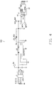


Classifications
-
- A—HUMAN NECESSITIES
- A24—TOBACCO; CIGARS; CIGARETTES; SIMULATED SMOKING DEVICES; SMOKERS' REQUISITES
- A24F—SMOKERS' REQUISITES; MATCH BOXES; SIMULATED SMOKING DEVICES
- A24F40/00—Electrically operated smoking devices; Component parts thereof; Manufacture thereof; Maintenance or testing thereof; Charging means specially adapted therefor
- A24F40/50—Control or monitoring
-
- H—ELECTRICITY
- H02—GENERATION; CONVERSION OR DISTRIBUTION OF ELECTRIC POWER
- H02J—ELECTRIC POWER NETWORKS; CIRCUIT ARRANGEMENTS OR SYSTEMS FOR SUPPLYING OR DISTRIBUTING ELECTRIC POWER; SYSTEMS FOR STORING ELECTRIC ENERGY
- H02J7/00—Circuit arrangements for charging or discharging batteries or for supplying loads from batteries
- H02J7/855—Circuit arrangements for charging or discharging batteries or for supplying loads from batteries with circuits adapted for supplying loads from the battery
-
- H—ELECTRICITY
- H02—GENERATION; CONVERSION OR DISTRIBUTION OF ELECTRIC POWER
- H02J—ELECTRIC POWER NETWORKS; CIRCUIT ARRANGEMENTS OR SYSTEMS FOR SUPPLYING OR DISTRIBUTING ELECTRIC POWER; SYSTEMS FOR STORING ELECTRIC ENERGY
- H02J7/00—Circuit arrangements for charging or discharging batteries or for supplying loads from batteries
- H02J7/90—Regulation of charging or discharging current or voltage
- H02J7/933—Regulation of charging or discharging current or voltage the cycle being controlled or terminated in response to electric parameters
-
- H—ELECTRICITY
- H02—GENERATION; CONVERSION OR DISTRIBUTION OF ELECTRIC POWER
- H02M—APPARATUS FOR CONVERSION BETWEEN AC AND AC, BETWEEN AC AND DC, OR BETWEEN DC AND DC, AND FOR USE WITH MAINS OR SIMILAR POWER SUPPLY SYSTEMS; CONVERSION OF DC OR AC INPUT POWER INTO SURGE OUTPUT POWER; CONTROL OR REGULATION THEREOF
- H02M3/00—Conversion of DC power input into DC power output
- H02M3/02—Conversion of DC power input into DC power output without intermediate conversion into AC
- H02M3/04—Conversion of DC power input into DC power output without intermediate conversion into AC by static converters
- H02M3/10—Conversion of DC power input into DC power output without intermediate conversion into AC by static converters using discharge tubes with control electrode or semiconductor devices with control electrode
- H02M3/145—Conversion of DC power input into DC power output without intermediate conversion into AC by static converters using discharge tubes with control electrode or semiconductor devices with control electrode using devices of a triode or transistor type requiring continuous application of a control signal
- H02M3/155—Conversion of DC power input into DC power output without intermediate conversion into AC by static converters using discharge tubes with control electrode or semiconductor devices with control electrode using devices of a triode or transistor type requiring continuous application of a control signal using semiconductor devices only
- H02M3/156—Conversion of DC power input into DC power output without intermediate conversion into AC by static converters using discharge tubes with control electrode or semiconductor devices with control electrode using devices of a triode or transistor type requiring continuous application of a control signal using semiconductor devices only with automatic control of output voltage or current, e.g. switching regulators
- H02M3/158—Conversion of DC power input into DC power output without intermediate conversion into AC by static converters using discharge tubes with control electrode or semiconductor devices with control electrode using devices of a triode or transistor type requiring continuous application of a control signal using semiconductor devices only with automatic control of output voltage or current, e.g. switching regulators including plural semiconductor devices as final control devices for a single load
-
- A—HUMAN NECESSITIES
- A24—TOBACCO; CIGARS; CIGARETTES; SIMULATED SMOKING DEVICES; SMOKERS' REQUISITES
- A24F—SMOKERS' REQUISITES; MATCH BOXES; SIMULATED SMOKING DEVICES
- A24F40/00—Electrically operated smoking devices; Component parts thereof; Manufacture thereof; Maintenance or testing thereof; Charging means specially adapted therefor
- A24F40/90—Arrangements or methods specially adapted for charging batteries thereof
-
- H—ELECTRICITY
- H02—GENERATION; CONVERSION OR DISTRIBUTION OF ELECTRIC POWER
- H02J—ELECTRIC POWER NETWORKS; CIRCUIT ARRANGEMENTS OR SYSTEMS FOR SUPPLYING OR DISTRIBUTING ELECTRIC POWER; SYSTEMS FOR STORING ELECTRIC ENERGY
- H02J2105/00—Networks for supplying or distributing electric power characterised by their spatial reach or by the load
- H02J2105/40—Networks for supplying or distributing electric power characterised by their spatial reach or by the load characterised by the loads connecting to the networks or being supplied by the networks
- H02J2105/44—Portable electronic devices
Definitions
- the subject matter herein generally relates to an electronic device, particularly relates to a voltage output circuit and an electronic cigarette.
- electronic cigarettes provide several additional functions besides a smoking function, such as a multimedia browsing function, a touch operation function, a navigation function, and a solar charging function, these additional functions are used for promoting a sale of the electronic cigarettes.
- a smoking function such as a multimedia browsing function, a touch operation function, a navigation function, and a solar charging function
- these additional functions are used for promoting a sale of the electronic cigarettes.
- the structure of the voltage output circuit in the current electronic cigarettes is complex and does not provide accurate and suitable driving voltages to different circuits corresponding to different additional functions.
- the present disclosure provided a voltage output circuit and an electronic cigarette, which can solve a problem of the voltage output circuit with a complicated structure, and does not provide accurate and suitable driving voltage.
- the present disclosure provides a voltage output circuit with a control chip and a step-down switch chip.
- the control chip includes a control signal input terminal and a modulation signal output terminal.
- the control signal input terminal of the control chip is connected with a first switch element, and is grounded through an initial ground resistor.
- the first switch element When the first switch element is energized, the first switch element generates an enable signal to the control chip.
- the step-down switch chip includes a first access terminal, a first control terminal, and a second access terminal.
- the first access terminal of the step-down switch chip receives a system power voltage
- the first control terminal of the step-down switch chip is connected with the modulation signal output terminal of the control chip.
- the control chip When the first switch element is energized, the control chip receives the enable signal and the modulation signal output terminal of the control chip outputs a pulse modulation signal to the first control terminal of the step-down switch chip, such that when receiving an effective level of the pulse modulation signal, the first control terminal of the step-down switch chip controls the first access terminal and the second access terminal to be conducted, and the voltage outputted by the second access terminal is less than the system power voltage.
- control signal input terminal receives the system power voltage through a first current limiting resistor and the first switch element, and/or the first control terminal is connected with the modulation signal output terminal of the control chip through a second current limiting resistor.
- control chip further includes a first power receiving terminal and a first ground terminal; the first power receiving terminal receives the system power voltage through a first filter resistor, and is connected with the first ground terminal of the control chip through the first filter capacitor and a second filter capacitor, which are connected with each other in parallel.
- the second access terminal of the step-down switch chip is connected with a thermal wire, and outputs a driving voltage for driving the thermal wire to generate heat.
- the control chip further includes an enable signal detection output terminal, a first current receiving terminal, and a second current receiving terminal;
- the voltage output circuit further includes a resistance detection circuit;
- the enable signal detection output terminal of the control chip is connected with the resistance detection circuit;
- the resistance detection circuit includes a third current limiting resistor, a fourth current limiting resistor, a first detection resistor, a second detection resistor, a third detection resistor, a third filter capacitor, a fourth filter capacitor, and a second switch element;
- the third access terminal of the second switch element receives the system power voltage, and is connected with the enable signal detection output terminal of the control chip through the third current limiting resistor;
- a second control terminal of the second switch element is connected with the enable signal detection output terminal of the control chip through the fourth current limiting resistor;
- a fourth access terminal of the second switch element is connected with the second access terminal of the step-down switch chip through the first detection resistor; one terminal of the second detection resistor is grounded through the third filter capacitor, and is connected with
- control chip further includes at least one indicator light control terminal; each indicator light control terminal is connected with an indicator circuit; the indicator circuit includes at least one fifth current limiting resistor and at least one LED. A cathode of each LED is connected with one indicator light control terminal through a fifth current limiting resistor, and an anode of each LED receives the system power voltage.
- the first switch element is an airflow sensor.
- a power terminal of the airflow sensor receives the system power voltage.
- the control signal input terminal of the first control chip is connected with a signal output terminal of the airflow sensor through the sixth current limiting resistor.
- the signal output terminal of the airflow sensor is grounded through the initial grounded resistor.
- the first control terminal of the step-down switch chip is connected with the modulation signal output terminal of the control chip through the second current limiting resistor.
- control chip further includes a first power receiving terminal and a first ground terminal.
- the first power receiving terminal of the control chip receives the system power voltage, and is grounded through a sixth filter capacitor.
- the first ground terminal is grounded.
- the first control terminal of the step-down switch chip receives the system power voltage through a seventh current limiting resistor.
- the second access terminal of the step-down switch chip is connected with a resistance detection terminal of the control chip through a fourth detection resistor.
- the resistance detection terminal is connected with one terminal of a divider resistor through the fourth detection resistor. Another terminal of the divider resistor is grounded.
- the second access terminal of the step-down switch chip is grounded through the divider resistor.
- the voltage output circuit further includes a voltage stabilizing module.
- a first terminal of the voltage stabilizing module is connected with a voltage output terminal of the control chip through a voltage stabilizing resistor.
- the first terminal of the voltage stabilizing module is connected with a second terminal of the voltage stabilizing module.
- the second terminal of the voltage stabilizing module is connected with a high voltage input terminal of the control chip.
- the present disclosure provides an electronic cigarette.
- the electronic cigarette includes the above recited voltage output circuit.
- the electronic cigarette further includes a chargeable battery.
- the chargeable battery provides the system power voltage.
- the electronic cigarette further includes a charging circuit.
- the charging circuit includes a connector and a charging chip.
- the charging chip includes a second power receiving terminal and a charging voltage output terminal.
- the second power receiving terminal is connected with an external power source through the connector.
- the charging voltage output terminal outputs a charging voltage to a positive terminal of the chargeable battery.
- the charging circuit further includes a charging protection chip.
- the charging protection chip includes a third power receiving terminal, a second ground terminal, a heat dissipation lump terminal, and a charging detection terminal.
- the third power receiving terminal of the charging protection chip is connected with the positive electrode of the chargeable battery.
- the second ground terminal of the charging protection chip is connected with a negative electrode of the chargeable battery.
- the heat dissipation lump terminal of the charging protection chip is connected with the second ground terminal of the charging protection chip.
- the charging detection terminal of the charging protection chip is grounded.
- the charging protection chip further includes a battery protection chip.
- the battery protection chip includes a charging input terminal, a third ground terminal, a fourth ground terminal, a fourth power receiving terminal, and an internal circuit power terminal.
- the charging input terminal is connected with a charging voltage output terminal of the charging chip, and the charging input terminal is grounded through a seventh capacitor.
- the third ground terminal and the fourth ground terminal are grounded.
- the internal circuit power terminal is grounded through an eighth capacitor.
- the fourth power receiving terminal is connected with a positive electrode of the chargeable battery.
- the negative electrode of the chargeable battery is grounded.
- the voltage output circuit and the electronic cigarette in the present disclosure outputs the pulse modulation signal to the step-down switch chip by the control chip, thus the step-down switch chip decreases the voltage based on the pulse modulation signal, and outputs a voltage less than the system power voltage to the load (such as the thermal wire). More flexibility of the voltage output circuit is provided.
- the structure of the voltage output circuit is made simple by using the control chip and the step-down switch chip.
- the present disclosure provides a voltage output circuit with a simple structure providing accurate and suitable voltages to different function circuits.
- FIG. 1 shows a first embodiment of the voltage output circuit 100.
- the voltage output circuit 100 includes a control chip U1 and a step-down switch chip U2.
- control chip U1 includes a control signal input terminal 11 and a modulation signal output terminal 12.
- the control signal input terminal 11 of the control chip U1 is connected with a first switch element, and is grounded through an initial ground resistor R1.
- the first switch element can be a switch element of a key, an airflow sensor, and so on.
- the airflow sensor is used for detecting a suction signal generated by user.
- the control signal input terminal 11 of the control chip U1 receives a system power voltage VCC_BAR through the first switch element SW1.
- the step-down switch chip U2 includes a first access terminal 21, a first control terminal 22, and a second access terminal 23.
- the first access terminal 21 of the step-down switch chip U2 receives the system power voltage VCC_BAR, and the first control terminal 22 of the step-down switch chip U2 is connected with the modulation signal output terminal 12 of the control chip U1.
- control chip U1 can be an N76E003-MSOP10*ICP integrated chip, not being limited thereto.
- the control signal input terminal 11 is one of AIN5/STADC/IC3/PWM3/P0-4 pins.
- the modulation signal output terminal 12 is one of P0-6/TXD/AIN3 pins.
- the step-down switch chip U2 can be a DTQ3205 integrated chip with positive channel metal oxide semiconductors (PMOSs), not being limited thereto.
- PMOSs positive channel metal oxide semiconductors
- the first access terminal 21 of the step-down switch chip U2 is a source electrode.
- the second access terminal 23 of the step-down switch chip U2 is a drain electrode.
- the first control terminal 22 is a gate electrode.
- the step-down switch chip U2 can be other models or other types of the integrated chip.
- the control signal input terminal 11 receives a high voltage level, thus the modulation signal output terminal 12 of the control chip U1 outputs a pulse modulation signal to the first control terminal 22 of the step-down switch chip U2.
- the first control terminal 22 of the step-down switch chip U2 controls the first access terminal 21 and the second access terminal 23 to be conducted.
- the output voltage VOUT outputted by the second access terminal 23 is less than the system power voltage VCC_BAR.
- control signal input terminal 11 of the control chip U1 receives the system power voltage VCC_BAR through a first current limiting resistor R2 and the first switch element SW1, and/or the first control terminal 22 of the step-down switch chip U2 is connected with the modulation signal output terminal 12 through a second current limiting resistor R3.
- control chip U1 can further include a first power receiving terminal 13 and a first ground terminal 14.
- the first power receiving terminal 13 of the control chip U1 receives the system power voltage VCC_BAR through a first filter resistor R4, and is connected with the first ground terminal 14 of the control chip U1 through a first filter capacitor C1 and a second filter capacitor C2, these being interconnected in parallel.
- the first power receiving terminal 13 and the first ground terminal 14 can be respectively a VDD pin and a GND pin of the integrated chip in a N76E003-MSOP10*ICP model, not being limited thereto.
- the second access terminal 23 of the step-down switch chip U2 is connected with a thermal wire (not shown), and outputs a driving voltage VOUT for driving the thermal wire to generate heat, an atomizing function is achieved.
- the voltage output circuit 100 in the embodiment provides the pulse modulation signal by the control chip U1 to the step-down switch chip U2, and the step-down switch chip U2 can adjust the pulse modulation signal for decreasing the voltage.
- the driving voltage VOUT being less than the system power voltage VCC_BAR is provided to a load, such as the thermal wire.
- the voltage output circuit 100 becomes more flexibility.
- the control chip U1 and the step-down switch chip U2 for outputting the driving voltage VOUT and the structure of the voltage output circuit 100 is simple.
- the first limiting resistor R1 and the second limiting resistor R2 for current-limiting protecting the circuit is against from being damage, and a stability of the voltage output circuit 100 is improved.
- FIG. 2 shows a second embodiment of the voltage output circuit 100.
- the voltage output circuit 100 according to the second embodiment is substantially the same as the voltage output circuit 100 according to the first embodiment, and the difference is that the control chip U1 further includes an enable signal detection output terminal 15, a first current receiving terminal 16, and a second current receiving terminal 17.
- the voltage output circuit 100 further includes a resistance detection circuit 110.
- the enable signal detection output terminal 15 of the control chip U1 is connected with the resistance detection circuit 110.
- the enable signal detection output terminal 15, the first current receiving terminal 16, and the second current receiving terminal 17 can be respectively one of AIN7/CLO/IC1/PWM1/P1 pins, one of AIN6/IC5/PWM5/P0-3 pins, and one of P0-6/TXD/AIN3 pins of the integrated chip in an N76E003-MSOP10*ICP model.
- the resistance detection circuit 110 includes a third current limiting resistor R5, a fourth current limiting resistor R6, a first detection resistor R7, a second detection resistor R8, a third detection resistor R9, a third filter capacitor C3, a fourth filter capacitor C4, and a second switch element SW2.
- a third access terminal of the second switch element SW2 receives the system power voltage VCC_BAR and is connected with the enable signal detection output terminal 15 of the control chip U1 through the third current limiting resistor R5.
- a second control terminal of the second switch element SW2 is connected with the enable signal detection output terminal 15 through the fourth current limiting resistor R6.
- a fourth access terminal of the second switch element SW2 is connected with the second access terminal 23 through the first detection resistor R7.
- One terminal of the second detection resistor R8 is grounded through the third filter capacitor C3, and is connected with the first current receiving terminal 16 of the control chip U1.
- the other terminal of the second detection resistor R8 is connected with the second access terminal 23 of the step-down switch chip U2.
- One terminal of the third detection resistor R9 is grounded through the fourth filter capacitor C4, and further is connected with the second current receiving terminal 17 of the control chip U1.
- Another terminal of the third detection resistor R9 is connected with the fourth access terminal of the second switch element SW2.
- the second switch element SW2 can be a PNP type transistor.
- the third access terminal of the second switch element SW2 is an emitter electrode
- the second control terminal of the second switch element SW2 is a base electrode
- the fourth access terminal of the second switch element SW2 is a collector electrode.
- the second switch element SW2 can be other types of transistor, such as a PMOS transistor.
- the enable signal detection output terminal 15 of the control chip U1 outputs a logic low signal
- the second switch element SW2 turns on.
- the first current receiving terminal 16 and the second current receiving terminal 17 of the control chip U1 respectively receive the current passing through the second detection resistor R8 and the third detection resistor R9, and acquire a resistance of the thermal wire based on difference in current between the first current receiving terminal 16 and the second current receiving terminal 17.
- the voltage output circuit 100 includes the resistance detection circuit 110.
- the resistance of the thermal wire is acquired based on a current difference outputted by the resistance detection circuit 110.
- a duty ratio of the pulse modulation signal can be adjusted based on the resistance of the thermal wire for adjusting the driving voltage VOUT provided to the thermal wire, more flexibility of the voltage output circuit 100 is provided.
- FIG. 3 shows a third embodiment of the voltage output circuit 100.
- the voltage output circuit 100 according to the third embodiment is substantially the same as the voltage output circuit 100 according to the second embodiment, and the difference is the control chip U1 further can include at least one indicator light control terminal 18. There are three shown in FIG. 3 . Each indicator light control terminal 18 is connected with an indicator circuit 200.
- the indicator circuit 200 includes at least one fifth current limiting resistor R10 and at least one light emitting diode (LED) D1.
- a cathode of each LED D1 is connected with one indicator light control terminal 18 through a fifth current limiting resistor R10, and an anode of each LED D1 receives the system power voltage VCC_BAR.
- the voltage output circuit 100 in the present embodiment further connects with the indicator circuit 200 and controls the LED D1 to be illuminated through the indicator light control terminal 18 for indicating power of a chargeable battery.
- the present disclosure further provides an electronic cigarette.
- the electronic cigarette includes the voltage output circuit.
- the embodiments of the voltage output circuit can refer FIGS. 1-3 and the corresponding descriptions, no more detailed description is provided.
- the electronic cigarette further includes a charging circuit 300.
- FIG. 4 shows a circuit diagram of the charging circuit 300.
- the charging circuit 300 includes a connector J1 and a charging chip U3.
- the charging chip U3 can include a second power receiving terminal 31 and a charging voltage output terminal 32.
- the second power receiving terminal 31 is connected with an external power source through the connector J1.
- the charging voltage output terminal 32 outputs a charging voltage to a positive terminal BAT+ of the chargeable battery.
- the charging chip U3 can be a BQ24040 integrated chip, not being limited thereto.
- the second power receiving terminal 31 and the charging voltage output terminal are an IN pin and an OUT pin of the BQ24040 integrated chip.
- the charging circuit 300 further includes a charging protection chip U4.
- the charging protection chip U4 includes a third power receiving terminal 41, a second ground terminal 42, a heat dissipation lump terminal 43, and a charging detection terminal 44.
- the third power receiving terminal 41 of the charging protection chip U4 is connected with the positive electrode BAT+ of the chargeable battery.
- the second ground terminal 42 of the charging protection chip U4 is connected with a negative electrode BAT- of the chargeable battery.
- the heat dissipation lump terminal 43 of the charging protection chip U4 is connected with the second ground terminal 42 of the charging protection chip U4.
- the charging detection terminal 44 of the charging protection chip U4 is grounded.
- the heat dissipation lump terminal of the charging protection chip U4 is used for decreasing a temperature of the charging protection chip U4 from being damaged by a high temperature.
- the heat dissipation lump terminal 43 of the charging protection chip U4 is connected with the second ground terminal 42 of the charging protection chip U4 for increasing a size of ground area of the charging protection chip U4, thus an over-current ability of the voltage output circuit 100.
- the charging protection chip U4 in the present disclosure protects the chargeable battery from being overcharged, or being short-circuited, or being over-discharged.
- the second ground terminal 42 of the charging protection chip U4 is connected with the negative electrode BAT- of the chargeable battery, and the charging detection terminal 44 of the charging protection chip U4 is grounded, thus the negative electrode BAR- of the chargeable battery is not connected directly to the ground.
- the charging protection chip U4 is disposed between the ground and the negative electrode BAR- of the chargeable battery. When charging or discharging the chargeable battery, the negative electrode BAR- of the chargeable battery needs to connect with the ground through the conducted charging protection chip U4.
- the charging protection chip U4 in the voltage output circuit 100 can detect the voltage or the current on its own pins or its own elements to determine whether the chargeable battery is in a state of being over-discharged or being overcharged. When in the state of being over-discharge or being overcharged, the connection between the negative electrode BAR- of the chargeable battery and the ground is disconnected for protecting the chargeable battery.
- the second ground terminal 42 of the charging protection chip U4 is connected with one terminal of the fifth filter capacitor C5, and another terminal of the fifth filter capacitor C5 is connected with the negative electrode BAR- of the chargeable battery.
- the fifth filter capacitor C5 filters the system power voltage VCC_BAR from the positive electrode BAR+ of the chargeable battery.
- the charging protection chip U4 is XB6006A2. As shown in FIG. 4 , the third power receiving terminal 41 of the charging protection chip U4 is a VDD terminal, the second ground terminal 42 is a GND terminal, the heat dissipation lump terminal 43 is an EPAD terminal, and the charging detection terminal 44 is a VM terminal.
- the electronic cigarette of the embodiment can automatically disconnect the chargeable battery from the charging chip U3 or a discharging path by the charging protection chip U4. Overcharging and/or over-discharging of the chargeable battery and the electronic cigarette are thus prevented, both the electronic cigarette and the chargeable battery are protected.
- the voltage output circuit 100 and the electronic cigarette outputs the pulse modulation signal to the step-down switch chip U2, and the step-down switch chip U2 decreases the voltage based on the pulse modulation signal and outputs the driving voltage VOUT being less than the system voltage VCC_BAR to the load, such as the thermal wire, more flexibility of the voltage output circuit 100 is provided.
- the control chip U1 and the step-down switch chip U2 the driving voltage VOUT can be outputted, the structure of the voltage output circuit 100 is simplified.
- FIG. 5 is a fourth embodiment of the voltage output circuit 400.
- the control chip U1 includes a control signal input terminal 11 and a modulation signal output terminal 12.
- the control signal input terminal 11 of the control chip U1 is connected with a first switch element, and is grounded through an initial grounded resistor R1.
- the control chip U1 further includes a first power receiving terminal 13 and a first grounding terminal 14.
- the first power receiving terminal 13 is connected with a positive electrode of the battery, and receives the system power voltage.
- the first power receiving terminal 13 is grounded through a sixth filter capacitor C6, and receives a stable voltage. Besides, the first grounding terminal 14 is grounded.
- the step-down switch chip U2 includes a first access terminal 21, a first control terminal 22, and a second access terminal 23.
- the first access terminal 21 of the step-down switch chip U2 receives the system power voltage VCC_BAR, and the first control terminal 22 of the step-down switch chip U2 is connected with the modulation signal output terminal 12 of the control chip U1.
- the first control terminal 22 of the step-down switch chip U2 receives the system power voltage through a seventh current limiting resistor R16.
- the second access terminal 23 of the step-down switch chip U2 is connected with a thermal wire for outputting a driving voltage to the thermal wire, and the thermal wire operates to generate heat.
- the step-down switch chip U2 can be a DTQ3205 integrated chip with positive channel metal oxide semiconductors (PMOSs), not being limited thereto.
- PMOSs positive channel metal oxide semiconductors
- the first access terminal 21 of the step-down switch chip U2 is a source electrode.
- the second access terminal 23 of the step-down switch chip U2 is a drain electrode.
- the first control terminal 22 is a gate electrode.
- the step-down switch chip U2 can be other models or other types of the integrated chip.
- the first switch element is an airflow sensor, such as a microphone.
- the first switch element detects a suction signal generated by user for determining whether the user is drawing on the electronic cigarette.
- the airflow sensor When the suction signal is detected by the airflow sensor, the airflow sensor generates an enable signal to the control chip U1.
- a power terminal 71 of the airflow sensor U7 is connected with a positive electrode of the chargeable battery, and is used for receiving the system power voltage VCC_BAR.
- the control signal input terminal 11 of the control chip U1 is connected with a signal output terminal 72 of the airflow sensor through a sixth current limiting resistor R11, and the signal output terminal 72 of the airflow sensor U7 is grounded through the initial ground resistor R1.
- a grounding terminal 73 of the airflow sensor U7 is grounded.
- the first grounding resistor R1 is used for pulling down and stabilizing the voltage.
- the first control terminal 22 of the step-down switch chip U2 is connected with the modulation signal output terminal 12 of the control chip U1 through a second current limiting resistor R3.
- the first control terminal 22 of the step-down switch chip U2 receives the system power voltage VCC_BAR through a seventh current limiting resistor R16.
- the second access terminal 23 of the step-down switch chip U2 is connected with a resistance detection terminal 19 of the control chip U1 through a fourth detection resistor R13.
- the resistance detection terminal 19 is connected with a terminal of a divider resistor R14 through the fourth detection resistor R13.
- Another terminal of the divider resistor R14 is grounded.
- the second access terminal 23 of the step-down switch chip U2 is grounded through the divider resistor R14.
- the fourth detection resistor R13 and the divider resistor R14 are set for detecting a resistance of the thermal wire, for determining whether the thermal wire is correctly installed.
- the fourth detection resistor R13 and the divider resistor R14 in the voltage output circuit 400 can be omitted, and the second access terminal 23 of the step-down switch unit U2 is directly connected with the resistance detection circuit 110 of the second embodiment, a current difference outputted by the resistance detection circuit 110 is used for acquiring a resistance of the thermal wire, and the duty ratio of the pulse modulation signal is adjusted based on the resistance of the thermal wire, the driving voltage VOUT provided to the thermal wire is adjusted, and more flexibility of the voltage output circuit 400 is improved.
- the voltage output circuit 400 in the embodiment further includes a voltage stabilizing module U5.
- a first terminal 51 of the voltage stabilizing module U5 is connected with a voltage output terminal 111 of the control chip U1 through a stabilizing resistor R15.
- the first terminal of the stabilizing module U5 is connected with a second terminal 52 of the stabilizing module U5.
- the second terminal 52 of the stabilizing module U5 is connected with a high voltage level input terminal 112 of the control chip.
- control chip U1 further includes at least one indicator light control terminal 18. Each indicator light control terminal 18 is connected with an indicator circuit 500.
- the indicator circuit 500 includes at least one fifth current limiting resistor R10 and at least one light emitting diode (LED) D1.
- a cathode of each LED D1 can be connected with one indicator light control terminal 18 through a fifth current limiting resistor R10.
- Cathodes of the LED D1 also can be connected with a single indicator light control terminal 18 through a single fifth current limiting resistor R10.
- each indicator light control terminal 18 is connected with a terminal of the LED D1 through the fifth current limiting resistor R10. Another terminal of the LED D1 is connected with the control signal input terminal 11 of the control chip U1.
- the terminals of the two LEDs D1 are connected with the indicator light control terminal 18 of the control chip U1 through a single fifth current limiting resistor R10, another terminals of the two LEDs D1 are connected with the control signal input terminal 11 of the control chip U1.
- a terminal of a third LED D1 is connected with the adjacent indicator light control terminal 18 of the control chip U1 through a second fifth current limiting resistor R10, another terminal of the third LED D1 is connected with the control signal input terminal 11 of the control chip U1.
- the three LEDs D1 can be illuminated or be dark under the control of the control signal input terminal 11 and the indicator light control terminal 18.
- the voltage output circuit 400 in the embodiment is connected with the indicator circuit 500, and controls the LED D1 to be illuminated through the indicator light control terminal 18, for indicating energy of the chargeable battery, for example, a energy is a green light, and a low energy is red light.
- the indicator circuit 500 also indicates a current power or an output voltage, for example, a high power is red light, and a low power is green light.
- the indicator circuit 500 also indicates a suction state of the user. When the user smokes the electronic cigarette, the LED D1 is illuminated. When the user stops smoking, the LED D1 is dark.
- a color of the indicator of the electronic cigarette is adjusted by controlling one or more of the LEDs D1 with different illuminated colors.
- a display color of the indicator of the electronic cigarette can be yellow by controlling the red LED D1 and the green LED D1 being illuminated.
- the adjusting manner is not limited thereto.
- the second access terminal 23 of the step-down switch chip U2 is connected with the thermal wire S and outputs the driving voltage for driving the thermal wire S to generate heat.
- the present disclosure also provides an electronic cigarette.
- the electronic cigarette includes the voltage output circuit 400.
- the embodiment of the voltage output circuit 400 can refer FIG. 5 and the corresponding description. No more detailed description is provided.
- the electronic cigarette further includes a charging circuit 600.
- FIG. 6 shows a circuit diagram of the charging circuit 600.
- the charging circuit 600 includes a connector J1 and a charging chip U3.
- the charging chip U3 includes a second power receiving terminal 31 and a charging voltage output terminal 32.
- the second power receiving terminal 31 is connected with an external power source through the connector J1.
- the charging voltage output terminal 32 outputs a charging voltage to a positive terminal BAT+ of the chargeable battery.
- the charging chip U3 can be a MP2602 integrated chip, not being limited thereto.
- the second power receiving terminal 31 and the charging voltage output terminal are a VIN pin and a BATT pin of the MP2602 integrated chip.
- the charging circuit 600 further includes a battery protection chip U6.
- the battery protection chip U6 is used for protecting the chargeable battery from being overcharged or being over-discharged.
- the battery protection chip U6 includes a charging input terminal 61, a third ground terminal 62, a fourth ground terminal 63, a fourth power receiving terminal 64, and an internal power supply terminal 65.
- the charging input terminal 61 is connected with charging voltage output terminal 32 of the charging chip U3 and is grounded through a seventh filter capacitor C7 for receiving a stability voltage.
- the third ground terminal 62 and the fourth ground terminal 63 are grounded.
- the internal power supply terminal 65 is grounded through an eighth capacitor C8.
- the fourth power receiving terminal 64 is connected with a positive electrode BAT+ of the chargeable battery.
- the battery protection chip U6 can be a CT2105 chip, but not being limited thereto.
- the charging input terminal 61 of the battery protection chip U6 is a VM pin
- the third ground terminal 62 and the fourth ground terminal 63 are GND pins.
- the fourth power receiving terminal 64 is a VDD pin
- the internal power supply terminal 65 is a VCC pin.
- the battery protection chip U6 detects that the chargeable battery is overcharged or over-discharged, the battery protection chip U6 disconnects a connection between the fourth power receiving terminal 64 and the chargeable battery, for disconnecting the chargeable battery from the voltage output circuit 400 and/or the charging circuit 600.
- the electronic cigarette can include a chargeable battery.
- the chargeable battery can be omitted, but not being limited thereto.
- the types of the chargeable battery can be a chargeable or a battery, such as, a lithium battery, an alkaline dry battery, a nickel metal hydride battery, a lead-acid battery, an iron nickel battery, a metal oxide battery, a zinc-silver battery, a zinc-nickel battery, a hydrogen-oxygen fuel battery, and a solar battery.
Landscapes
- Engineering & Computer Science (AREA)
- Power Engineering (AREA)
- Charge And Discharge Circuits For Batteries Or The Like (AREA)
- Dc-Dc Converters (AREA)
- Control Of Voltage And Current In General (AREA)
Abstract
Description
- The subject matter herein generally relates to an electronic device, particularly relates to a voltage output circuit and an electronic cigarette.
- In order to improve users experience, electronic cigarettes provide several additional functions besides a smoking function, such as a multimedia browsing function, a touch operation function, a navigation function, and a solar charging function, these additional functions are used for promoting a sale of the electronic cigarettes.
- For achieving the additional functions of the electronic cigarette, it is necessary to provide different voltages to different circuits corresponding to the additional functions, especially the atomizing function which is the basic function of the electronic cigarettes and needs to be guaranteed.
- The structure of the voltage output circuit in the current electronic cigarettes is complex and does not provide accurate and suitable driving voltages to different circuits corresponding to different additional functions.
- In view of the above, the present disclosure provided a voltage output circuit and an electronic cigarette, which can solve a problem of the voltage output circuit with a complicated structure, and does not provide accurate and suitable driving voltage.
- The aspects of the present disclosure are as follows:
- The present disclosure provides a voltage output circuit with a control chip and a step-down switch chip. The control chip includes a control signal input terminal and a modulation signal output terminal. The control signal input terminal of the control chip is connected with a first switch element, and is grounded through an initial ground resistor. When the first switch element is energized, the first switch element generates an enable signal to the control chip. The step-down switch chip includes a first access terminal, a first control terminal, and a second access terminal. The first access terminal of the step-down switch chip receives a system power voltage, the first control terminal of the step-down switch chip is connected with the modulation signal output terminal of the control chip. When the first switch element is energized, the control chip receives the enable signal and the modulation signal output terminal of the control chip outputs a pulse modulation signal to the first control terminal of the step-down switch chip, such that when receiving an effective level of the pulse modulation signal, the first control terminal of the step-down switch chip controls the first access terminal and the second access terminal to be conducted, and the voltage outputted by the second access terminal is less than the system power voltage.
- In one embodiment, the control signal input terminal receives the system power voltage through a first current limiting resistor and the first switch element, and/or the first control terminal is connected with the modulation signal output terminal of the control chip through a second current limiting resistor.
- In one embodiment, the control chip further includes a first power receiving terminal and a first ground terminal; the first power receiving terminal receives the system power voltage through a first filter resistor, and is connected with the first ground terminal of the control chip through the first filter capacitor and a second filter capacitor, which are connected with each other in parallel.
- In one embodiment, the second access terminal of the step-down switch chip is connected with a thermal wire, and outputs a driving voltage for driving the thermal wire to generate heat.
- In one embodiment, the control chip further includes an enable signal detection output terminal, a first current receiving terminal, and a second current receiving terminal; the voltage output circuit further includes a resistance detection circuit; the enable signal detection output terminal of the control chip is connected with the resistance detection circuit; the resistance detection circuit includes a third current limiting resistor, a fourth current limiting resistor, a first detection resistor, a second detection resistor, a third detection resistor, a third filter capacitor, a fourth filter capacitor, and a second switch element; the third access terminal of the second switch element receives the system power voltage, and is connected with the enable signal detection output terminal of the control chip through the third current limiting resistor; a second control terminal of the second switch element is connected with the enable signal detection output terminal of the control chip through the fourth current limiting resistor; a fourth access terminal of the second switch element is connected with the second access terminal of the step-down switch chip through the first detection resistor; one terminal of the second detection resistor is grounded through the third filter capacitor, and is connected with the first current receiving terminal of the control chip; another terminal of the second detection resistor is connected with the second access terminal of the step-down switch chip; one terminal of the third detection resistor is grounded through the fourth filter capacitor, and is connected with the second current receiving terminal of the control chip; another terminal of the third detection resistor is connected with the fourth access terminal of the second switch element.
- In one embodiment, the control chip further includes at least one indicator light control terminal; each indicator light control terminal is connected with an indicator circuit; the indicator circuit includes at least one fifth current limiting resistor and at least one LED. A cathode of each LED is connected with one indicator light control terminal through a fifth current limiting resistor, and an anode of each LED receives the system power voltage.
- In one embodiment, the first switch element is an airflow sensor. A power terminal of the airflow sensor receives the system power voltage. The control signal input terminal of the first control chip is connected with a signal output terminal of the airflow sensor through the sixth current limiting resistor. The signal output terminal of the airflow sensor is grounded through the initial grounded resistor. And/or, the first control terminal of the step-down switch chip is connected with the modulation signal output terminal of the control chip through the second current limiting resistor.
- In one embodiment, the control chip further includes a first power receiving terminal and a first ground terminal.
- The first power receiving terminal of the control chip receives the system power voltage, and is grounded through a sixth filter capacitor. The first ground terminal is grounded.
- In one embodiment, the first control terminal of the step-down switch chip receives the system power voltage through a seventh current limiting resistor. The second access terminal of the step-down switch chip is connected with a resistance detection terminal of the control chip through a fourth detection resistor. The resistance detection terminal is connected with one terminal of a divider resistor through the fourth detection resistor. Another terminal of the divider resistor is grounded. The second access terminal of the step-down switch chip is grounded through the divider resistor.
- In one embodiment, the voltage output circuit further includes a voltage stabilizing module. A first terminal of the voltage stabilizing module is connected with a voltage output terminal of the control chip through a voltage stabilizing resistor. The first terminal of the voltage stabilizing module is connected with a second terminal of the voltage stabilizing module. The second terminal of the voltage stabilizing module is connected with a high voltage input terminal of the control chip.
- The present disclosure provides an electronic cigarette. The electronic cigarette includes the above recited voltage output circuit.
- In one embodiment, the electronic cigarette further includes a chargeable battery. The chargeable battery provides the system power voltage.
- In one embodiment, the electronic cigarette further includes a charging circuit. The charging circuit includes a connector and a charging chip. The charging chip includes a second power receiving terminal and a charging voltage output terminal. The second power receiving terminal is connected with an external power source through the connector. The charging voltage output terminal outputs a charging voltage to a positive terminal of the chargeable battery.
- In one embodiment, the charging circuit further includes a charging protection chip. The charging protection chip includes a third power receiving terminal, a second ground terminal, a heat dissipation lump terminal, and a charging detection terminal. The third power receiving terminal of the charging protection chip is connected with the positive electrode of the chargeable battery. The second ground terminal of the charging protection chip is connected with a negative electrode of the chargeable battery. The heat dissipation lump terminal of the charging protection chip is connected with the second ground terminal of the charging protection chip. The charging detection terminal of the charging protection chip is grounded.
- In one embodiment, the charging protection chip further includes a battery protection chip. The battery protection chip includes a charging input terminal, a third ground terminal, a fourth ground terminal, a fourth power receiving terminal, and an internal circuit power terminal.
- The charging input terminal is connected with a charging voltage output terminal of the charging chip, and the charging input terminal is grounded through a seventh capacitor. The third ground terminal and the fourth ground terminal are grounded. The internal circuit power terminal is grounded through an eighth capacitor. The fourth power receiving terminal is connected with a positive electrode of the chargeable battery. The negative electrode of the chargeable battery is grounded.
- The voltage output circuit and the electronic cigarette has the following advantages:
- The voltage output circuit and the electronic cigarette in the present disclosure outputs the pulse modulation signal to the step-down switch chip by the control chip, thus the step-down switch chip decreases the voltage based on the pulse modulation signal, and outputs a voltage less than the system power voltage to the load (such as the thermal wire). More flexibility of the voltage output circuit is provided. The structure of the voltage output circuit is made simple by using the control chip and the step-down switch chip.
- Implementations of the present disclosure will now be described, by way of example only, with reference to the attached figures.
-
FIG. 1 is a circuit diagram illustrating a first embodiment of a voltage output circuit. -
FIG. 2 is a circuit diagram illustrating a second embodiment of a voltage output circuit. -
FIG. 3 is a circuit diagram illustrating a third embodiment of a voltage output circuit. -
FIG. 4 is a circuit diagram illustrating a fourth embodiment of a charging circuit. -
FIG. 5 is a circuit diagram illustrating a fifth embodiment of a voltage output circuit. -
FIG. 6 is a circuit diagram illustrating a sixth embodiment of a charging circuit. - It will be appreciated that for simplicity and clarity of illustration, where appropriate, reference numerals have been repeated among the different figures to indicate corresponding or analogous elements. In addition, numerous specific details are set forth in order to provide a thorough understanding of the embodiments described herein. However, it will be understood by those of ordinary skill in the art that the embodiments described herein can be practiced without these specific details. In other instances, methods, procedures, and components have not been described in detail so as not to obscure the related relevant feature being described. The drawings are not necessarily to scale and the proportions of certain parts may be exaggerated to better illustrate details and features. The description is not to be considered as limiting the scope of the embodiments described herein.
- The term "comprising" means "including, but not necessarily limited to"; it specifically indicates open-ended inclusion or membership in a so-described combination, group, series, and the like. The disclosure is illustrated by way of example and not by way of limitation in the figures of the accompanying drawings in which like references indicate similar elements. It should be noted that references to "an" or "one" embodiment in this disclosure are not necessarily to the same embodiment, and such references can mean "at least one."
- The present disclosure provides a voltage output circuit with a simple structure providing accurate and suitable voltages to different function circuits.
-
FIG. 1 shows a first embodiment of thevoltage output circuit 100. As shown inFIG. 1 , thevoltage output circuit 100 includes a control chip U1 and a step-down switch chip U2. - In detail, the control chip U1 includes a control
signal input terminal 11 and a modulationsignal output terminal 12. The controlsignal input terminal 11 of the control chip U1 is connected with a first switch element, and is grounded through an initial ground resistor R1. In one embodiment, the first switch element can be a switch element of a key, an airflow sensor, and so on. The airflow sensor is used for detecting a suction signal generated by user. When the first switch element is a key, the controlsignal input terminal 11 of the control chip U1 receives a system power voltage VCC_BAR through the first switch element SW1. When the key is pressed, the first switch element SW1 turns on, the system power voltage VCC_BAR is applied to the controlsignal input terminal 11 of the control chip U1, the control chip U1 outputs a modulation signal to the step-down switch chip U2 through the modulationsignal output terminal 12. In detail, the step-down switch chip U2 includes afirst access terminal 21, afirst control terminal 22, and asecond access terminal 23. Thefirst access terminal 21 of the step-down switch chip U2 receives the system power voltage VCC_BAR, and thefirst control terminal 22 of the step-down switch chip U2 is connected with the modulationsignal output terminal 12 of the control chip U1. - In one embodiment, the control chip U1 can be an N76E003-MSOP10*ICP integrated chip, not being limited thereto. When the control chip U1 is N76E003-MSOP10*ICP integrated chip, the control
signal input terminal 11 is one of AIN5/STADC/IC3/PWM3/P0-4 pins. The modulationsignal output terminal 12 is one of P0-6/TXD/AIN3 pins. - In one embodiment, the step-down switch chip U2 can be a DTQ3205 integrated chip with positive channel metal oxide semiconductors (PMOSs), not being limited thereto. When the step-down switch chip U2 is a DTQ3205 integrated chip with PMOSs, the
first access terminal 21 of the step-down switch chip U2 is a source electrode. Thesecond access terminal 23 of the step-down switch chip U2 is a drain electrode. Thefirst control terminal 22 is a gate electrode. In other embodiments, the step-down switch chip U2 can be other models or other types of the integrated chip. - In detail, when the first switch element SW1 turns on, the control
signal input terminal 11 receives a high voltage level, thus the modulationsignal output terminal 12 of the control chip U1 outputs a pulse modulation signal to thefirst control terminal 22 of the step-down switch chip U2. Thus, when receiving an effective voltage level (for example, an effective voltage level of the PMOS is low voltage level), thefirst control terminal 22 of the step-down switch chip U2 controls thefirst access terminal 21 and thesecond access terminal 23 to be conducted. The output voltage VOUT outputted by thesecond access terminal 23 is less than the system power voltage VCC_BAR. - In one embodiment, the control
signal input terminal 11 of the control chip U1 receives the system power voltage VCC_BAR through a first current limiting resistor R2 and the first switch element SW1, and/or thefirst control terminal 22 of the step-down switch chip U2 is connected with the modulationsignal output terminal 12 through a second current limiting resistor R3. - In one embodiment, the control chip U1 can further include a first
power receiving terminal 13 and afirst ground terminal 14. The firstpower receiving terminal 13 of the control chip U1 receives the system power voltage VCC_BAR through a first filter resistor R4, and is connected with thefirst ground terminal 14 of the control chip U1 through a first filter capacitor C1 and a second filter capacitor C2, these being interconnected in parallel. - In one embodiment, the first
power receiving terminal 13 and thefirst ground terminal 14 can be respectively a VDD pin and a GND pin of the integrated chip in a N76E003-MSOP10*ICP model, not being limited thereto. - In one embodiment, the
second access terminal 23 of the step-down switch chip U2 is connected with a thermal wire (not shown), and outputs a driving voltage VOUT for driving the thermal wire to generate heat, an atomizing function is achieved. - The
voltage output circuit 100 in the embodiment provides the pulse modulation signal by the control chip U1 to the step-down switch chip U2, and the step-down switch chip U2 can adjust the pulse modulation signal for decreasing the voltage. The driving voltage VOUT being less than the system power voltage VCC_BAR is provided to a load, such as the thermal wire. Thus, thevoltage output circuit 100 becomes more flexibility. Using the control chip U1 and the step-down switch chip U2 for outputting the driving voltage VOUT, and the structure of thevoltage output circuit 100 is simple. In addition, using the first limiting resistor R1 and the second limiting resistor R2 for current-limiting protecting, the circuit is against from being damage, and a stability of thevoltage output circuit 100 is improved. -
FIG. 2 shows a second embodiment of thevoltage output circuit 100. As shown inFIG. 2 , thevoltage output circuit 100 according to the second embodiment is substantially the same as thevoltage output circuit 100 according to the first embodiment, and the difference is that the control chip U1 further includes an enable signaldetection output terminal 15, a first current receivingterminal 16, and a second current receivingterminal 17. Thevoltage output circuit 100 further includes aresistance detection circuit 110. The enable signaldetection output terminal 15 of the control chip U1 is connected with theresistance detection circuit 110. - In one embodiment, the enable signal
detection output terminal 15, the first current receivingterminal 16, and the second current receivingterminal 17 can be respectively one of AIN7/CLO/IC1/PWM1/P1 pins, one of AIN6/IC5/PWM5/P0-3 pins, and one of P0-6/TXD/AIN3 pins of the integrated chip in an N76E003-MSOP10*ICP model. - The
resistance detection circuit 110 includes a third current limiting resistor R5, a fourth current limiting resistor R6, a first detection resistor R7, a second detection resistor R8, a third detection resistor R9, a third filter capacitor C3, a fourth filter capacitor C4, and a second switch element SW2. A third access terminal of the second switch element SW2 receives the system power voltage VCC_BAR and is connected with the enable signaldetection output terminal 15 of the control chip U1 through the third current limiting resistor R5. A second control terminal of the second switch element SW2 is connected with the enable signaldetection output terminal 15 through the fourth current limiting resistor R6. A fourth access terminal of the second switch element SW2 is connected with thesecond access terminal 23 through the first detection resistor R7. One terminal of the second detection resistor R8 is grounded through the third filter capacitor C3, and is connected with the first current receivingterminal 16 of the control chip U1. The other terminal of the second detection resistor R8 is connected with thesecond access terminal 23 of the step-down switch chip U2. One terminal of the third detection resistor R9 is grounded through the fourth filter capacitor C4, and further is connected with the second current receivingterminal 17 of the control chip U1. Another terminal of the third detection resistor R9 is connected with the fourth access terminal of the second switch element SW2. - In one embodiment, the second switch element SW2 can be a PNP type transistor. The third access terminal of the second switch element SW2 is an emitter electrode, the second control terminal of the second switch element SW2 is a base electrode, and the fourth access terminal of the second switch element SW2 is a collector electrode. In other embodiments, the second switch element SW2 can be other types of transistor, such as a PMOS transistor.
- Using the PNP transistor as the second switch element SW2 as an example for explaining, in detail, when the first switch element SW1 turns off (cuts-off), the enable signal
detection output terminal 15 of the control chip U1 outputs a logic low signal, the second switch element SW2 turns on. The first current receivingterminal 16 and the second current receivingterminal 17 of the control chip U1 respectively receive the current passing through the second detection resistor R8 and the third detection resistor R9, and acquire a resistance of the thermal wire based on difference in current between the first current receivingterminal 16 and the second current receivingterminal 17. - In one embodiment, the
voltage output circuit 100 includes theresistance detection circuit 110. The resistance of the thermal wire is acquired based on a current difference outputted by theresistance detection circuit 110. Thus, a duty ratio of the pulse modulation signal can be adjusted based on the resistance of the thermal wire for adjusting the driving voltage VOUT provided to the thermal wire, more flexibility of thevoltage output circuit 100 is provided. -
FIG. 3 shows a third embodiment of thevoltage output circuit 100. As shown inFIG. 3 , thevoltage output circuit 100 according to the third embodiment is substantially the same as thevoltage output circuit 100 according to the second embodiment, and the difference is the control chip U1 further can include at least one indicatorlight control terminal 18. There are three shown inFIG. 3 . Each indicatorlight control terminal 18 is connected with anindicator circuit 200. - The
indicator circuit 200 includes at least one fifth current limiting resistor R10 and at least one light emitting diode (LED) D1. A cathode of each LED D1 is connected with one indicatorlight control terminal 18 through a fifth current limiting resistor R10, and an anode of each LED D1 receives the system power voltage VCC_BAR. - The
voltage output circuit 100 in the present embodiment further connects with theindicator circuit 200 and controls the LED D1 to be illuminated through the indicatorlight control terminal 18 for indicating power of a chargeable battery. - The present disclosure further provides an electronic cigarette. The electronic cigarette includes the voltage output circuit. The embodiments of the voltage output circuit can refer
FIGS. 1-3 and the corresponding descriptions, no more detailed description is provided. - In the embodiment, the electronic cigarette further includes a charging
circuit 300.FIG. 4 shows a circuit diagram of the chargingcircuit 300. As shown inFIG. 4 , the chargingcircuit 300 includes a connector J1 and a charging chip U3. - In detail, the charging chip U3 can include a second
power receiving terminal 31 and a chargingvoltage output terminal 32. The secondpower receiving terminal 31 is connected with an external power source through the connector J1. The chargingvoltage output terminal 32 outputs a charging voltage to a positive terminal BAT+ of the chargeable battery. - In one embodiment, the charging chip U3 can be a BQ24040 integrated chip, not being limited thereto. The second
power receiving terminal 31 and the charging voltage output terminal are an IN pin and an OUT pin of the BQ24040 integrated chip. - In one embodiment, the charging
circuit 300 further includes a charging protection chip U4. The charging protection chip U4 includes a thirdpower receiving terminal 41, asecond ground terminal 42, a heatdissipation lump terminal 43, and a charging detection terminal 44. - In detail, the third
power receiving terminal 41 of the charging protection chip U4 is connected with the positive electrode BAT+ of the chargeable battery. Thesecond ground terminal 42 of the charging protection chip U4 is connected with a negative electrode BAT- of the chargeable battery. The heatdissipation lump terminal 43 of the charging protection chip U4 is connected with thesecond ground terminal 42 of the charging protection chip U4. The charging detection terminal 44 of the charging protection chip U4 is grounded. The heat dissipation lump terminal of the charging protection chip U4 is used for decreasing a temperature of the charging protection chip U4 from being damaged by a high temperature. The heatdissipation lump terminal 43 of the charging protection chip U4 is connected with thesecond ground terminal 42 of the charging protection chip U4 for increasing a size of ground area of the charging protection chip U4, thus an over-current ability of thevoltage output circuit 100. - In detail, the charging protection chip U4 in the present disclosure protects the chargeable battery from being overcharged, or being short-circuited, or being over-discharged. The
second ground terminal 42 of the charging protection chip U4 is connected with the negative electrode BAT- of the chargeable battery, and the charging detection terminal 44 of the charging protection chip U4 is grounded, thus the negative electrode BAR- of the chargeable battery is not connected directly to the ground. The charging protection chip U4 is disposed between the ground and the negative electrode BAR- of the chargeable battery. When charging or discharging the chargeable battery, the negative electrode BAR- of the chargeable battery needs to connect with the ground through the conducted charging protection chip U4. Thus, the charging protection chip U4 in thevoltage output circuit 100 can detect the voltage or the current on its own pins or its own elements to determine whether the chargeable battery is in a state of being over-discharged or being overcharged. When in the state of being over-discharge or being overcharged, the connection between the negative electrode BAR- of the chargeable battery and the ground is disconnected for protecting the chargeable battery. - In one embodiment, the
second ground terminal 42 of the charging protection chip U4 is connected with one terminal of the fifth filter capacitor C5, and another terminal of the fifth filter capacitor C5 is connected with the negative electrode BAR- of the chargeable battery. The fifth filter capacitor C5 filters the system power voltage VCC_BAR from the positive electrode BAR+ of the chargeable battery. - In one embodiment, the charging protection chip U4 is XB6006A2. As shown in
FIG. 4 , the thirdpower receiving terminal 41 of the charging protection chip U4 is a VDD terminal, thesecond ground terminal 42 is a GND terminal, the heatdissipation lump terminal 43 is an EPAD terminal, and the charging detection terminal 44 is a VM terminal. - The electronic cigarette of the embodiment can automatically disconnect the chargeable battery from the charging chip U3 or a discharging path by the charging protection chip U4. Overcharging and/or over-discharging of the chargeable battery and the electronic cigarette are thus prevented, both the electronic cigarette and the chargeable battery are protected.
- The
voltage output circuit 100 and the electronic cigarette outputs the pulse modulation signal to the step-down switch chip U2, and the step-down switch chip U2 decreases the voltage based on the pulse modulation signal and outputs the driving voltage VOUT being less than the system voltage VCC_BAR to the load, such as the thermal wire, more flexibility of thevoltage output circuit 100 is provided. Using the control chip U1 and the step-down switch chip U2, the driving voltage VOUT can be outputted, the structure of thevoltage output circuit 100 is simplified. -
FIG. 5 is a fourth embodiment of the voltage output circuit 400. The control chip U1 includes a controlsignal input terminal 11 and a modulationsignal output terminal 12. The controlsignal input terminal 11 of the control chip U1 is connected with a first switch element, and is grounded through an initial grounded resistor R1. In detail, the control chip U1 further includes a firstpower receiving terminal 13 and afirst grounding terminal 14. The firstpower receiving terminal 13 is connected with a positive electrode of the battery, and receives the system power voltage. The firstpower receiving terminal 13 is grounded through a sixth filter capacitor C6, and receives a stable voltage. Besides, thefirst grounding terminal 14 is grounded. - In detail, the step-down switch chip U2 includes a
first access terminal 21, afirst control terminal 22, and asecond access terminal 23. Thefirst access terminal 21 of the step-down switch chip U2 receives the system power voltage VCC_BAR, and thefirst control terminal 22 of the step-down switch chip U2 is connected with the modulationsignal output terminal 12 of the control chip U1. Optionally, thefirst control terminal 22 of the step-down switch chip U2 receives the system power voltage through a seventh current limiting resistor R16. Thesecond access terminal 23 of the step-down switch chip U2 is connected with a thermal wire for outputting a driving voltage to the thermal wire, and the thermal wire operates to generate heat. - In one embodiment, the step-down switch chip U2 can be a DTQ3205 integrated chip with positive channel metal oxide semiconductors (PMOSs), not being limited thereto. When the step-down switch chip U2 can be a DTQ3205 integrated chip with PMOSs, the
first access terminal 21 of the step-down switch chip U2 is a source electrode. Thesecond access terminal 23 of the step-down switch chip U2 is a drain electrode. Thefirst control terminal 22 is a gate electrode. In other embodiments, the step-down switch chip U2 can be other models or other types of the integrated chip. - In one embodiment, the first switch element is an airflow sensor, such as a microphone. The first switch element detects a suction signal generated by user for determining whether the user is drawing on the electronic cigarette. When the suction signal is detected by the airflow sensor, the airflow sensor generates an enable signal to the control chip U1.
- As shown in
FIG. 5 , a power terminal 71 of the airflow sensor U7 is connected with a positive electrode of the chargeable battery, and is used for receiving the system power voltage VCC_BAR. The controlsignal input terminal 11 of the control chip U1 is connected with asignal output terminal 72 of the airflow sensor through a sixth current limiting resistor R11, and thesignal output terminal 72 of the airflow sensor U7 is grounded through the initial ground resistor R1. A grounding terminal 73 of the airflow sensor U7 is grounded. The first grounding resistor R1 is used for pulling down and stabilizing the voltage. When the suction action is detected by the airflow sensor U7, the airflow sensor U7 outputs the enable signal to the controlsignal input terminal 11 of the control chip U1 through thesignal output terminal 72. When the control chip U1 receives the enable signal, the pulse modulation signal is outputted to the step-down switch chip U2 through the modulationsignal output terminal 12. - In detail, the
first control terminal 22 of the step-down switch chip U2 is connected with the modulationsignal output terminal 12 of the control chip U1 through a second current limiting resistor R3. Thefirst control terminal 22 of the step-down switch chip U2 receives the system power voltage VCC_BAR through a seventh current limiting resistor R16. - In detail, the
second access terminal 23 of the step-down switch chip U2 is connected with aresistance detection terminal 19 of the control chip U1 through a fourth detection resistor R13. Theresistance detection terminal 19 is connected with a terminal of a divider resistor R14 through the fourth detection resistor R13. Another terminal of the divider resistor R14 is grounded. Thesecond access terminal 23 of the step-down switch chip U2 is grounded through the divider resistor R14. In one embodiment, the fourth detection resistor R13 and the divider resistor R14 are set for detecting a resistance of the thermal wire, for determining whether the thermal wire is correctly installed. Optionally, the fourth detection resistor R13 and the divider resistor R14 in the voltage output circuit 400 can be omitted, and thesecond access terminal 23 of the step-down switch unit U2 is directly connected with theresistance detection circuit 110 of the second embodiment, a current difference outputted by theresistance detection circuit 110 is used for acquiring a resistance of the thermal wire, and the duty ratio of the pulse modulation signal is adjusted based on the resistance of the thermal wire, the driving voltage VOUT provided to the thermal wire is adjusted, and more flexibility of the voltage output circuit 400 is improved. - Optionally, the voltage output circuit 400 in the embodiment further includes a voltage stabilizing module U5. A first terminal 51 of the voltage stabilizing module U5 is connected with a
voltage output terminal 111 of the control chip U1 through a stabilizing resistor R15. The first terminal of the stabilizing module U5 is connected with asecond terminal 52 of the stabilizing module U5. Thesecond terminal 52 of the stabilizing module U5 is connected with a high voltagelevel input terminal 112 of the control chip. By setting the stabilizing module U5, the voltage output circuit 400 in the embodiment stabilizes an internal voltage of the control chip U1 at a predetermined voltage, for preventing the control chip U1 being damaged while operated under an instability voltage. - Optionally, the control chip U1 further includes at least one indicator
light control terminal 18. Each indicatorlight control terminal 18 is connected with an indicator circuit 500. - The indicator circuit 500 includes at least one fifth current limiting resistor R10 and at least one light emitting diode (LED) D1. A cathode of each LED D1 can be connected with one indicator
light control terminal 18 through a fifth current limiting resistor R10. Cathodes of the LED D1 also can be connected with a single indicatorlight control terminal 18 through a single fifth current limiting resistor R10. - As shown in
FIG. 5 , there are two indicatorlight control terminals 18. Each indicatorlight control terminal 18 is connected with a terminal of the LED D1 through the fifth current limiting resistor R10. Another terminal of the LED D1 is connected with the controlsignal input terminal 11 of the control chip U1. Optionally, as shown inFIG. 5 , the terminals of the two LEDs D1 are connected with the indicatorlight control terminal 18 of the control chip U1 through a single fifth current limiting resistor R10, another terminals of the two LEDs D1 are connected with the controlsignal input terminal 11 of the control chip U1. A terminal of a third LED D1 is connected with the adjacent indicatorlight control terminal 18 of the control chip U1 through a second fifth current limiting resistor R10, another terminal of the third LED D1 is connected with the controlsignal input terminal 11 of the control chip U1. The three LEDs D1 can be illuminated or be dark under the control of the controlsignal input terminal 11 and the indicatorlight control terminal 18. - The voltage output circuit 400 in the embodiment is connected with the indicator circuit 500, and controls the LED D1 to be illuminated through the indicator
light control terminal 18, for indicating energy of the chargeable battery, for example, a energy is a green light, and a low energy is red light. Besides, the indicator circuit 500 also indicates a current power or an output voltage, for example, a high power is red light, and a low power is green light. The indicator circuit 500 also indicates a suction state of the user. When the user smokes the electronic cigarette, the LED D1 is illuminated. When the user stops smoking, the LED D1 is dark. In one embodiment, by setting LEDs D1 with different illuminated colors, a color of the indicator of the electronic cigarette is adjusted by controlling one or more of the LEDs D1 with different illuminated colors. For example, a display color of the indicator of the electronic cigarette can be yellow by controlling the red LED D1 and the green LED D1 being illuminated. The adjusting manner is not limited thereto. - In one embodiment, the
second access terminal 23 of the step-down switch chip U2 is connected with the thermal wire S and outputs the driving voltage for driving the thermal wire S to generate heat. - The present disclosure also provides an electronic cigarette. The electronic cigarette includes the voltage output circuit 400. The embodiment of the voltage output circuit 400 can refer
FIG. 5 and the corresponding description. No more detailed description is provided. - In one embodiment, the electronic cigarette further includes a charging circuit 600. Referring to
FIG. 6, FIG. 6 shows a circuit diagram of the charging circuit 600. The charging circuit 600 includes a connector J1 and a charging chip U3. - In detail, the charging chip U3 includes a second
power receiving terminal 31 and a chargingvoltage output terminal 32. The secondpower receiving terminal 31 is connected with an external power source through the connector J1. The chargingvoltage output terminal 32 outputs a charging voltage to a positive terminal BAT+ of the chargeable battery. In one embodiment, the charging chip U3 can be a MP2602 integrated chip, not being limited thereto. The secondpower receiving terminal 31 and the charging voltage output terminal are a VIN pin and a BATT pin of the MP2602 integrated chip. - Optionally, in another embodiment, the charging circuit 600 further includes a battery protection chip U6. The battery protection chip U6 is used for protecting the chargeable battery from being overcharged or being over-discharged. The battery protection chip U6 includes a charging
input terminal 61, a third ground terminal 62, a fourth ground terminal 63, a fourth power receiving terminal 64, and an internalpower supply terminal 65. In one embodiment, the charginginput terminal 61 is connected with chargingvoltage output terminal 32 of the charging chip U3 and is grounded through a seventh filter capacitor C7 for receiving a stability voltage. The third ground terminal 62 and the fourth ground terminal 63 are grounded. The internalpower supply terminal 65 is grounded through an eighth capacitor C8. The fourth power receiving terminal 64 is connected with a positive electrode BAT+ of the chargeable battery. A negative electrode of the chargeable battery is grounded. Optionally, the battery protection chip U6 can be a CT2105 chip, but not being limited thereto. When the battery protection chip U6 is the CT2105 chip, the charginginput terminal 61 of the battery protection chip U6 is a VM pin, the third ground terminal 62 and the fourth ground terminal 63 are GND pins. The fourth power receiving terminal 64 is a VDD pin, and the internalpower supply terminal 65 is a VCC pin. In one embodiment, when the battery protection chip U6 detects that the chargeable battery is overcharged or over-discharged, the battery protection chip U6 disconnects a connection between the fourth power receiving terminal 64 and the chargeable battery, for disconnecting the chargeable battery from the voltage output circuit 400 and/or the charging circuit 600. - Besides, in one embodiment, the electronic cigarette can include a chargeable battery. In other embodiments, the chargeable battery can be omitted, but not being limited thereto. The types of the chargeable battery can be a chargeable or a battery, such as, a lithium battery, an alkaline dry battery, a nickel metal hydride battery, a lead-acid battery, an iron nickel battery, a metal oxide battery, a zinc-silver battery, a zinc-nickel battery, a hydrogen-oxygen fuel battery, and a solar battery.
- While various and preferred embodiments have been described the disclosure is not limited thereto. On the contrary, various modifications and similar arrangements (as would be apparent to those skilled in the art) are also intended to be covered. Therefore, the scope of the appended claims should be accorded the broadest interpretation so as to encompass all such modifications and similar arrangements.
Claims (15)
- A voltage output circuit (100, 400) comprising:a control chip (U1) with a control signal input terminal (11) and a modulation signal output terminal (12), the control signal input terminal (11) of the control chip (U1) receives a system power voltage through a first switch element, and is grounded through an initial ground resistor (R1); the first switch element generates an enable signal to the control chip (U1) when being energized; anda step-down switch chip (U2) with a first access terminal (21), a first control terminal (22), and a second access terminal (23); the first access terminal (21) of the step-down switch chip (U2) receives the system power voltage, the first control terminal (22) of the step-down switch chip (U2) is connected with the modulation signal output terminal (12) of the control chip (U1);wherein when the first switch element is energized, the control chip (U1) receives the enable signal, and the modulation signal output terminal (12) of the control chip (U1) outputs a pulse modulation signal to the first control terminal (22) of the step-down switch chip (U2); when receiving the effective pulse modulation signal at the first control terminal (21) of the step-down switch chip (U1), the first access terminal (21) and the second access terminal (23) are conducted; the output voltage of the second access terminal (23) is less than the system power voltage.
- The voltage output circuit of claim 1, wherein the control signal input terminal (11) of the control chip (U1) receives the system power voltage through a first current limiting resistor (R2) and the first switch element (SW1); and/or the first control terminal (22) of the step-down switch chip (U2) is electrically connected with the modulation signal output terminal (12) of the control chip (U1) through a second current limiting resistor (R3).
- The voltage output circuit of claim 1, wherein the control chip (U1) further comprises a first power receiving terminal (13) and a first ground terminal (14); the first power receiving terminal (13) of the control chip (U1) receives the system power voltage through a first filter resistor (R4), and is further connected with the first ground terminal (14) of the control chip (U1) through a first filter capacitor (C1) and a second filter capacitor (C2), which are connected with each other in parallel.
- The voltage output circuit of claim 1, wherein the second access terminal (23) of the step-down switch chip (U2) is connected with a thermal wire (S) and outputs a driving voltage for driving the thermal wire (S) to generate heat.
- The voltage output circuit of claim 1 or 4, wherein the control chip (U1) further comprises an enable signal detection output terminal (15), a first current receiving terminal (16), and a second current receiving terminal (17); the voltage output circuit (100, 400) further comprises a resistance detection circuit (110); the enable signal detection output terminal (15) of the control chip (U1) is connected with the resistance detection circuit (110); the resistance detection circuit (110) comprises third current limiting resistor (R5), a fourth current limiting resistor (R6), a first detection resistor (R7), a second detection resistor (R8), a third detection resistor (R9), a third filter capacitor (C3), a fourth filter capacitor (C4), and a second switch element; the third access terminal of the second switch element receives the system power voltage, and is connected with the enable signal detection output terminal (15) of the control chip (U1) through the third current limiting resistor (R5); a second control terminal of the second switch element is connected with the enable signal detection output terminal (15) of the control chip (U1) through the fourth current limiting resistor (R6); a fourth access terminal of the second switch element is connected with the second access terminal (23) of the step-down switch chip (U2) through the first detection resistor (R7); one terminal of the second detection resistor (R8) is grounded through the third filter capacitor (C3), and another terminal of the second detection resistor (R8) is connected with the second access terminal (23) of the step-down switch chip (U2); one terminal of the third detection resistor (R9) is grounded through the fourth filter capacitor (C4), and further is connected with the second current receiving terminal (17) of the control chip (U1); another terminal of the third detection resistor (R9) is connected with the fourth access terminal of the second switch element.
- The voltage output circuit of claim 1, wherein the control chip (U1) further comprises at least one indicator light control terminal (18); each indicator light control terminal (18) is connected with an indicator circuit (200); the indicator circuit (200) comprises at least one fifth current limiting resistor (R10) and at least one LED (D1); a cathode of each LED (D1) is connected with one indicator light control terminal (18) through a fifth current limiting resistor (R10), and an anode of each LED (D1) receives the system power voltage.
- The voltage output circuit of claim 1, wherein the first switch element is an airflow sensor; a power terminal of the airflow sensor receives the system voltage; the control signal input terminal (11) of the control chip (U1) is electrically connected with a signal output terminal (72) of the airflow sensor through a sixth current limiting resistor (R12), the signal output terminal (72) of the airflow sensor is grounded through the initial ground resistor (R1); and/or the first control terminal (22) of the step-down switch chip (U2) is connected with the modulation signal output terminal (12) of the control chip (U1).
- The voltage output circuit of claim 7, wherein the control chip (U1) further comprises a first power receiving terminal (13) and a first ground terminal (14); the first power receiving terminal (13) of the control chip (U1) receives the system power voltage, and is grounded through a sixth filter capacitor (C6); the first ground terminal (14) is grounded.
- The voltage output circuit of claim 8, wherein the first control terminal of the step-down switch chip (U2) receives the system power voltage through a seventh current limit resistor (R16), the second access terminal (23) of the step-down switch chip (U2) is connected with a resistance detection terminal (19) of the control chip (U1) through a fourth detection resistor (R13); the resistance detection terminal (19) is connected with a terminal of a divider resistor (R14) through the fourth detection resistor (R13), another terminal of the divider resistor (R14) is grounded; the second access terminal (23) of the step-down switch chip (U2) is grounded through the divider resistor (R14).
- The voltage output circuit of claim 7, wherein the voltage output circuit (100, 400) further comprises a voltage stabilizing module (U5); a first terminal (51) of the voltage stabilizing module (U5) is connected with a voltage output terminal (111) of the control chip (U1) through a stabilizing resistor (R15); the first terminal (51) of the stabilizing module (U5) is connected with a second terminal (52) of the stabilizing module (U5); the second terminal (52) of the stabilizing module (U5) is connected with a high voltage level input terminal (112) of the control chip.
- An electronic cigarette comprising the voltage output circuit of any one of claims 1-10.
- The electronic cigarette of claim 11, wherein the electronic cigarette further comprises a chargeable battery; the chargeable battery provides the system power voltage.
- The electronic cigarette of claim 12, wherein the electronic cigarette further comprises a charging circuit (300); the charging circuit (300) a connector (J1) and a charging chip (U3); the charging chip (U3) comprises a second power receiving terminal (31) and a charging voltage output terminal (32); the second power receiving terminal (31) is connected with an external power source through the connector (J1); the charging voltage output terminal (32) outputs a charging voltage to a positive terminal of the chargeable battery.
- The electronic cigarette of claim 13, wherein the electronic cigarette further comprises a charging protection chip (U4); the charging protection chip (U4) comprises a third power receiving terminal (41), a second ground terminal (42), a heat dissipation lump terminal (43), and a charging detection terminal (44); the third power receiving terminal (41) of the charging protection chip (U4) is connected with the positive electrode of the chargeable battery; the second ground terminal of the charging protection chip (U4) is connected with a negative electrode of the chargeable battery; the heat dissipation lump terminal (43) of the charging protection chip (U4) is connected with the second ground terminal (42) of the charging protection chip (U4); the charging detection terminal (44) of the charging protection chip (U4) is grounded.
- The electronic cigarette of claim 13, wherein the charging circuit (300) further comprises a battery protection chip (U6); the battery protection chip (U6) comprises a charging input terminal (61), a third ground terminal (62), a fourth ground terminal (63), a fourth power receiving terminal (64), and an internal power supply terminal (65); the charging input terminal (61) is connected with charging voltage output terminal (32) of the charging chip (U3), and is grounded through a seventh filter capacitor (C7) for receiving a stability voltage; the third ground terminal (62) and the fourth ground terminal (63) are grounded; the internal power supply terminal (65) is grounded through an eighth capacitor (C8); the fourth power receiving terminal (64) is connected with a positive electrode of the chargeable batter; a negative electrode of the chargeable battery is grounded.
Applications Claiming Priority (2)
| Application Number | Priority Date | Filing Date | Title |
|---|---|---|---|
| CN201820241963.4U CN209132654U (en) | 2018-02-09 | 2018-02-09 | Voltage follower circuit and electronic cigarette |
| PCT/CN2018/096121 WO2019153653A1 (en) | 2018-02-09 | 2018-07-18 | Voltage output circuit and electronic cigarette |
Publications (2)
| Publication Number | Publication Date |
|---|---|
| EP3750419A1 true EP3750419A1 (en) | 2020-12-16 |
| EP3750419A4 EP3750419A4 (en) | 2021-11-24 |
Family
ID=67226728
Family Applications (1)
| Application Number | Title | Priority Date | Filing Date |
|---|---|---|---|
| EP18905764.9A Pending EP3750419A4 (en) | 2018-02-09 | 2018-07-18 | VOLTAGE OUTPUT CIRCUIT AND ELECTRONIC CIGARETTE |
Country Status (4)
| Country | Link |
|---|---|
| US (2) | US11602177B2 (en) |
| EP (1) | EP3750419A4 (en) |
| CN (2) | CN209132654U (en) |
| WO (1) | WO2019153653A1 (en) |
Cited By (1)
| Publication number | Priority date | Publication date | Assignee | Title |
|---|---|---|---|---|
| US12520880B2 (en) | 2021-01-18 | 2026-01-13 | Altria Client Services Llc | Heat-not-burn (HNB) aerosol-generating devices including energy based heater control, and methods of controlling a heater |
Families Citing this family (14)
| Publication number | Priority date | Publication date | Assignee | Title |
|---|---|---|---|---|
| CN207265866U (en) * | 2017-08-21 | 2018-04-20 | 卓尔悦欧洲控股有限公司 | Booster circuit, cell apparatus and electronic cigarette |
| US10959459B2 (en) * | 2018-05-16 | 2021-03-30 | Rai Strategic Holdings, Inc. | Voltage regulator for an aerosol delivery device |
| FR3082071A1 (en) * | 2018-05-29 | 2019-12-06 | Stmicroelectronics S.R.L | ELECTRONIC SUPPLY CIRCUIT |
| CN112438440A (en) * | 2019-08-26 | 2021-03-05 | 常州市派腾电子技术服务有限公司 | Control circuit and control method of electronic cigarette and electronic cigarette |
| CN113067453A (en) * | 2019-12-13 | 2021-07-02 | 常州市派腾电子技术服务有限公司 | Voltage output circuit, electronic cigarette, and control method and device of electronic cigarette |
| CN111109659B (en) * | 2019-12-31 | 2025-09-05 | 深圳雷炎科技有限公司 | Heating wire power control method, heating wire power control circuit and electronic cigarette |
| CN111011936B (en) * | 2019-12-31 | 2025-09-09 | 深圳雷炎科技有限公司 | Heating wire control method, heating wire control circuit and electronic cigarette |
| CN112021666B (en) * | 2020-08-31 | 2023-10-27 | 歌尔微电子股份有限公司 | Electronic cigarette circuit and electronic cigarette |
| US11164431B1 (en) * | 2020-09-15 | 2021-11-02 | Marvin Reid | Facility security system |
| WO2022205825A1 (en) * | 2021-04-02 | 2022-10-06 | 北京航天雷特机电工程有限公司 | Microwave generating circuit and microwave generating device |
| CN117241686A (en) * | 2021-05-10 | 2023-12-15 | 日本烟草产业株式会社 | Power supply unit for aerosol generating device |
| CN114424838B (en) * | 2021-12-15 | 2024-06-28 | 海南摩尔兄弟科技有限公司 | Battery pole and electronic atomization device |
| WO2023246413A1 (en) * | 2022-06-21 | 2023-12-28 | 西安稳先半导体科技有限责任公司 | System control circuit, indication assembly, and electronic atomization apparatus |
| CN116584712A (en) * | 2023-06-20 | 2023-08-15 | 卓尔悦国际控股有限公司 | Aerosol generating device |
Family Cites Families (19)
| Publication number | Priority date | Publication date | Assignee | Title |
|---|---|---|---|---|
| US4771358A (en) * | 1987-11-09 | 1988-09-13 | Walker Magnetics Group, Inc. | Magnetic chuck controller |
| US20090033293A1 (en) * | 2007-08-01 | 2009-02-05 | Intersil Americas Inc. | Voltage converter with combined capacitive voltage divider, buck converter and battery charger |
| CN202303455U (en) * | 2011-09-15 | 2012-07-04 | 夏志强 | Special integrated circuit assembly for electronic cigarette lighter |
| US8820330B2 (en) * | 2011-10-28 | 2014-09-02 | Evolv, Llc | Electronic vaporizer that simulates smoking with power control |
| TW201328150A (en) * | 2011-12-27 | 2013-07-01 | Hon Hai Prec Ind Co Ltd | Buck circuit |
| CN203341005U (en) * | 2013-05-15 | 2013-12-18 | 杭州联声电子有限公司 | Chargeable electronic cigarette controller |
| US10004262B2 (en) * | 2013-06-26 | 2018-06-26 | Huizhou Kimree Technology Co., Ltd. Shenzhen Branch | Electronic cigarette and method for supplying constant power therein |
| KR101549626B1 (en) * | 2013-12-20 | 2015-09-03 | (주)엠에스테크비젼 | Charge cable |
| JP2015128336A (en) * | 2013-12-27 | 2015-07-09 | 株式会社東芝 | Power-supply circuit and electronic apparatus |
| US9968137B2 (en) * | 2014-07-31 | 2018-05-15 | Zhiyong Xiang | Electronic cigarette and charging method therefor |
| WO2016123897A1 (en) * | 2015-02-02 | 2016-08-11 | 佛山市顺德区美的电热电器制造有限公司 | Electromagnetic heating control circuit and electromagnetic heating device |
| CN204790671U (en) * | 2015-07-15 | 2015-11-18 | 深圳市新宜康科技有限公司 | Electron cigarette heating power stable control circuit |
| CN105955094B (en) * | 2015-12-25 | 2019-03-08 | 深圳瀚星翔科技有限公司 | A kind of electronic cigarette power regulation control circuit |
| CN205902801U (en) * | 2016-08-12 | 2017-01-25 | 深圳市海派特光伏科技有限公司 | Voltage step -up and step -down typed integrated circuit and electron cigarette |
| CN205883045U (en) * | 2016-08-12 | 2017-01-11 | 深圳市海派特光伏科技有限公司 | Switch tube drive integrated circuit and electron cigarette |
| CN206371515U (en) * | 2016-11-30 | 2017-08-04 | 广州周立功单片机科技有限公司 | Electronic cigarette |
| CN106343617B (en) * | 2016-11-30 | 2019-04-30 | 广州周立功单片机科技有限公司 | Electronic cigarette control method, device and electronic cigarette |
| US10667554B2 (en) * | 2017-09-18 | 2020-06-02 | Rai Strategic Holdings, Inc. | Smoking articles |
| CN107589608A (en) * | 2017-09-25 | 2018-01-16 | 惠科股份有限公司 | Display device and method for eliminating shutdown ghost |
-
2018
- 2018-02-09 CN CN201820241963.4U patent/CN209132654U/en active Active
- 2018-07-18 WO PCT/CN2018/096121 patent/WO2019153653A1/en not_active Ceased
- 2018-07-18 EP EP18905764.9A patent/EP3750419A4/en active Pending
- 2018-07-18 CN CN201890000106.3U patent/CN210038590U/en active Active
-
2020
- 2020-08-04 US US16/984,902 patent/US11602177B2/en active Active
-
2023
- 2023-02-06 US US18/106,462 patent/US11871796B2/en active Active
Cited By (1)
| Publication number | Priority date | Publication date | Assignee | Title |
|---|---|---|---|---|
| US12520880B2 (en) | 2021-01-18 | 2026-01-13 | Altria Client Services Llc | Heat-not-burn (HNB) aerosol-generating devices including energy based heater control, and methods of controlling a heater |
Also Published As
| Publication number | Publication date |
|---|---|
| CN210038590U (en) | 2020-02-07 |
| EP3750419A4 (en) | 2021-11-24 |
| US20200359700A1 (en) | 2020-11-19 |
| WO2019153653A1 (en) | 2019-08-15 |
| US11871796B2 (en) | 2024-01-16 |
| US11602177B2 (en) | 2023-03-14 |
| CN209132654U (en) | 2019-07-19 |
| US20230180846A1 (en) | 2023-06-15 |
Similar Documents
| Publication | Publication Date | Title |
|---|---|---|
| US11871796B2 (en) | Voltage output circuit for electronic cigarette and electronic cigarette using circuit | |
| CN206432703U (en) | Super-charge super-discharge protection circuit, protection device, battery management system and electric automobile | |
| US11889863B2 (en) | Voltage output circuit and electronic cigarette | |
| US9438049B2 (en) | Control circuit and method for a portable charging carrying case for providing uninterruptible power to charge electronic cigarette batteries | |
| JP3777022B2 (en) | Battery charger | |
| JP4380927B2 (en) | Overcharge protection circuit | |
| US10622819B2 (en) | Rechargeable battery protection integrated circuit, rechargeable battery protection device, and battery pack | |
| JP3665574B2 (en) | Charge / discharge control circuit and rechargeable power supply | |
| CN101465557B (en) | Portable device and battery pack for the same | |
| US20200221780A1 (en) | Overheat protection circuit, electronic cigarette and electronic equipment | |
| JPH08167430A (en) | Battery protection circuit | |
| CN210471028U (en) | Control circuit of electronic cigarette and electronic cigarette thereof | |
| WO2019169968A1 (en) | Battery protection circuit and electronic cigarette | |
| CN220190493U (en) | Lithium battery charging activation circuit and PCM protection board | |
| JP2003174720A (en) | Protection circuit for secondary battery and protection circuit IC | |
| CN112438440A (en) | Control circuit and control method of electronic cigarette and electronic cigarette | |
| CN109922563B (en) | Emergency light device and emergency light control integrated circuit | |
| CN215990263U (en) | Integrated circuit and system for battery charging and discharging protection | |
| CN110198060A (en) | Super-charge super-discharge protects circuit | |
| CN211377872U (en) | Voltage output circuit and electronic cigarette | |
| CN114794588A (en) | Battery protection circuit, battery pack and electron cigarette | |
| CN113839448B (en) | A battery management circuit and energy storage system | |
| CN220605591U (en) | Anti-interference charging awakening circuit based on BMS | |
| CN218183047U (en) | Boost charging circuit | |
| CN119253542A (en) | A battery over-discharge protection circuit and control method thereof |
Legal Events
| Date | Code | Title | Description |
|---|---|---|---|
| STAA | Information on the status of an ep patent application or granted ep patent |
Free format text: STATUS: THE INTERNATIONAL PUBLICATION HAS BEEN MADE |
|
| PUAI | Public reference made under article 153(3) epc to a published international application that has entered the european phase |
Free format text: ORIGINAL CODE: 0009012 |
|
| STAA | Information on the status of an ep patent application or granted ep patent |
Free format text: STATUS: REQUEST FOR EXAMINATION WAS MADE |
|
| 17P | Request for examination filed |
Effective date: 20200909 |
|
| AK | Designated contracting states |
Kind code of ref document: A1 Designated state(s): AL AT BE BG CH CY CZ DE DK EE ES FI FR GB GR HR HU IE IS IT LI LT LU LV MC MK MT NL NO PL PT RO RS SE SI SK SM TR |
|
| AX | Request for extension of the european patent |
Extension state: BA ME |
|
| DAV | Request for validation of the european patent (deleted) | ||
| DAX | Request for extension of the european patent (deleted) | ||
| A4 | Supplementary search report drawn up and despatched |
Effective date: 20211022 |
|
| RIC1 | Information provided on ipc code assigned before grant |
Ipc: A24F 40/90 20200101ALN20211018BHEP Ipc: A24F 40/50 20200101ALI20211018BHEP Ipc: G05F 1/56 20060101ALI20211018BHEP Ipc: H02J 7/00 20060101ALI20211018BHEP Ipc: G05B 19/042 20060101AFI20211018BHEP |