EP3749624B1 - Solar control coatings with quadruple metallic layers - Google Patents
Solar control coatings with quadruple metallic layers Download PDFInfo
- Publication number
- EP3749624B1 EP3749624B1 EP19708914.7A EP19708914A EP3749624B1 EP 3749624 B1 EP3749624 B1 EP 3749624B1 EP 19708914 A EP19708914 A EP 19708914A EP 3749624 B1 EP3749624 B1 EP 3749624B1
- Authority
- EP
- European Patent Office
- Prior art keywords
- layer
- primer
- over
- thickness
- metallic
- Prior art date
- Legal status (The legal status is an assumption and is not a legal conclusion. Google has not performed a legal analysis and makes no representation as to the accuracy of the status listed.)
- Active
Links
- 238000000576 coating method Methods 0.000 title description 55
- XLOMVQKBTHCTTD-UHFFFAOYSA-N Zinc monoxide Chemical compound [Zn]=O XLOMVQKBTHCTTD-UHFFFAOYSA-N 0.000 claims description 62
- 239000011787 zinc oxide Substances 0.000 claims description 31
- 239000000203 mixture Substances 0.000 claims description 20
- 239000000758 substrate Substances 0.000 claims description 18
- 239000010936 titanium Substances 0.000 claims description 18
- 229910052751 metal Inorganic materials 0.000 claims description 13
- 239000002184 metal Substances 0.000 claims description 13
- RYGMFSIKBFXOCR-UHFFFAOYSA-N Copper Chemical compound [Cu] RYGMFSIKBFXOCR-UHFFFAOYSA-N 0.000 claims description 12
- 229910052802 copper Inorganic materials 0.000 claims description 12
- 239000010949 copper Substances 0.000 claims description 12
- 229910052782 aluminium Inorganic materials 0.000 claims description 11
- 229910052709 silver Inorganic materials 0.000 claims description 11
- 239000004332 silver Substances 0.000 claims description 11
- BNEMLSQAJOPTGK-UHFFFAOYSA-N zinc;dioxido(oxo)tin Chemical compound [Zn+2].[O-][Sn]([O-])=O BNEMLSQAJOPTGK-UHFFFAOYSA-N 0.000 claims description 11
- 229910045601 alloy Inorganic materials 0.000 claims description 10
- 239000000956 alloy Substances 0.000 claims description 10
- XAGFODPZIPBFFR-UHFFFAOYSA-N aluminium Chemical compound [Al] XAGFODPZIPBFFR-UHFFFAOYSA-N 0.000 claims description 10
- 230000005540 biological transmission Effects 0.000 claims description 9
- RTAQQCXQSZGOHL-UHFFFAOYSA-N Titanium Chemical group [Ti] RTAQQCXQSZGOHL-UHFFFAOYSA-N 0.000 claims description 8
- 229910052710 silicon Inorganic materials 0.000 claims description 8
- 239000010703 silicon Substances 0.000 claims description 8
- 229910052719 titanium Inorganic materials 0.000 claims description 8
- XUIMIQQOPSSXEZ-UHFFFAOYSA-N Silicon Chemical compound [Si] XUIMIQQOPSSXEZ-UHFFFAOYSA-N 0.000 claims description 7
- PXHVJJICTQNCMI-UHFFFAOYSA-N Nickel Chemical compound [Ni] PXHVJJICTQNCMI-UHFFFAOYSA-N 0.000 claims description 4
- VYZAMTAEIAYCRO-UHFFFAOYSA-N Chromium Chemical compound [Cr] VYZAMTAEIAYCRO-UHFFFAOYSA-N 0.000 claims description 3
- QCWXUUIWCKQGHC-UHFFFAOYSA-N Zirconium Chemical compound [Zr] QCWXUUIWCKQGHC-UHFFFAOYSA-N 0.000 claims description 3
- 229910052804 chromium Inorganic materials 0.000 claims description 3
- 239000011651 chromium Substances 0.000 claims description 3
- 229910052726 zirconium Inorganic materials 0.000 claims description 3
- 229910017052 cobalt Inorganic materials 0.000 claims description 2
- 239000010941 cobalt Substances 0.000 claims description 2
- GUTLYIVDDKVIGB-UHFFFAOYSA-N cobalt atom Chemical compound [Co] GUTLYIVDDKVIGB-UHFFFAOYSA-N 0.000 claims description 2
- 229910052759 nickel Inorganic materials 0.000 claims description 2
- 229910000838 Al alloy Inorganic materials 0.000 claims 1
- 229910000531 Co alloy Inorganic materials 0.000 claims 1
- 229910000990 Ni alloy Inorganic materials 0.000 claims 1
- CSDREXVUYHZDNP-UHFFFAOYSA-N alumanylidynesilicon Chemical compound [Al].[Si] CSDREXVUYHZDNP-UHFFFAOYSA-N 0.000 claims 1
- 229910000623 nickel–chromium alloy Inorganic materials 0.000 claims 1
- 239000010410 layer Substances 0.000 description 236
- 239000011248 coating agent Substances 0.000 description 49
- 239000011521 glass Substances 0.000 description 29
- 239000000463 material Substances 0.000 description 23
- 229910003107 Zn2SnO4 Inorganic materials 0.000 description 16
- 239000011701 zinc Substances 0.000 description 15
- HCHKCACWOHOZIP-UHFFFAOYSA-N Zinc Chemical compound [Zn] HCHKCACWOHOZIP-UHFFFAOYSA-N 0.000 description 14
- ATJFFYVFTNAWJD-UHFFFAOYSA-N Tin Chemical compound [Sn] ATJFFYVFTNAWJD-UHFFFAOYSA-N 0.000 description 12
- 229910052718 tin Inorganic materials 0.000 description 12
- 229910044991 metal oxide Inorganic materials 0.000 description 11
- 150000004706 metal oxides Chemical class 0.000 description 11
- 229910052725 zinc Inorganic materials 0.000 description 11
- VYPSYNLAJGMNEJ-UHFFFAOYSA-N Silicium dioxide Chemical compound O=[Si]=O VYPSYNLAJGMNEJ-UHFFFAOYSA-N 0.000 description 9
- 229910001092 metal group alloy Inorganic materials 0.000 description 9
- 238000000034 method Methods 0.000 description 9
- GWEVSGVZZGPLCZ-UHFFFAOYSA-N Titan oxide Chemical compound O=[Ti]=O GWEVSGVZZGPLCZ-UHFFFAOYSA-N 0.000 description 8
- 230000005855 radiation Effects 0.000 description 7
- KDLHZDBZIXYQEI-UHFFFAOYSA-N Palladium Chemical compound [Pd] KDLHZDBZIXYQEI-UHFFFAOYSA-N 0.000 description 6
- -1 polysiloxane Polymers 0.000 description 6
- 229910001887 tin oxide Inorganic materials 0.000 description 6
- 229910052581 Si3N4 Inorganic materials 0.000 description 5
- BQCADISMDOOEFD-UHFFFAOYSA-N Silver Chemical compound [Ag] BQCADISMDOOEFD-UHFFFAOYSA-N 0.000 description 5
- 239000011247 coating layer Substances 0.000 description 5
- 239000007789 gas Substances 0.000 description 5
- HQVNEWCFYHHQES-UHFFFAOYSA-N silicon nitride Chemical compound N12[Si]34N5[Si]62N3[Si]51N64 HQVNEWCFYHHQES-UHFFFAOYSA-N 0.000 description 5
- XKRFYHLGVUSROY-UHFFFAOYSA-N Argon Chemical compound [Ar] XKRFYHLGVUSROY-UHFFFAOYSA-N 0.000 description 4
- 229910001128 Sn alloy Inorganic materials 0.000 description 4
- 230000005670 electromagnetic radiation Effects 0.000 description 4
- 239000005329 float glass Substances 0.000 description 4
- 238000004519 manufacturing process Methods 0.000 description 4
- 150000004767 nitrides Chemical class 0.000 description 4
- 229910052814 silicon oxide Inorganic materials 0.000 description 4
- 238000004544 sputter deposition Methods 0.000 description 4
- XOLBLPGZBRYERU-UHFFFAOYSA-N tin dioxide Chemical compound O=[Sn]=O XOLBLPGZBRYERU-UHFFFAOYSA-N 0.000 description 4
- 229910001297 Zn alloy Inorganic materials 0.000 description 3
- PNEYBMLMFCGWSK-UHFFFAOYSA-N aluminium oxide Inorganic materials [O-2].[O-2].[O-2].[Al+3].[Al+3] PNEYBMLMFCGWSK-UHFFFAOYSA-N 0.000 description 3
- QVGXLLKOCUKJST-UHFFFAOYSA-N atomic oxygen Chemical compound [O] QVGXLLKOCUKJST-UHFFFAOYSA-N 0.000 description 3
- 238000005229 chemical vapour deposition Methods 0.000 description 3
- 238000000151 deposition Methods 0.000 description 3
- 230000008021 deposition Effects 0.000 description 3
- PCHJSUWPFVWCPO-UHFFFAOYSA-N gold Chemical compound [Au] PCHJSUWPFVWCPO-UHFFFAOYSA-N 0.000 description 3
- 229910052737 gold Inorganic materials 0.000 description 3
- 239000010931 gold Substances 0.000 description 3
- 239000001301 oxygen Substances 0.000 description 3
- 229910052760 oxygen Inorganic materials 0.000 description 3
- 229910052763 palladium Inorganic materials 0.000 description 3
- 238000005240 physical vapour deposition Methods 0.000 description 3
- 239000000377 silicon dioxide Substances 0.000 description 3
- 238000006124 Pilkington process Methods 0.000 description 2
- 229910052786 argon Inorganic materials 0.000 description 2
- 229910052738 indium Inorganic materials 0.000 description 2
- APFVFJFRJDLVQX-UHFFFAOYSA-N indium atom Chemical compound [In] APFVFJFRJDLVQX-UHFFFAOYSA-N 0.000 description 2
- 239000002346 layers by function Substances 0.000 description 2
- 229920000058 polyacrylate Polymers 0.000 description 2
- 229920000139 polyethylene terephthalate Polymers 0.000 description 2
- 239000005020 polyethylene terephthalate Substances 0.000 description 2
- QHGNHLZPVBIIPX-UHFFFAOYSA-N tin(ii) oxide Chemical class [Sn]=O QHGNHLZPVBIIPX-UHFFFAOYSA-N 0.000 description 2
- 238000002834 transmittance Methods 0.000 description 2
- ZOXJGFHDIHLPTG-UHFFFAOYSA-N Boron Chemical compound [B] ZOXJGFHDIHLPTG-UHFFFAOYSA-N 0.000 description 1
- PWHULOQIROXLJO-UHFFFAOYSA-N Manganese Chemical compound [Mn] PWHULOQIROXLJO-UHFFFAOYSA-N 0.000 description 1
- 229910000676 Si alloy Inorganic materials 0.000 description 1
- 229910001347 Stellite Inorganic materials 0.000 description 1
- 230000003667 anti-reflective effect Effects 0.000 description 1
- 229910052787 antimony Inorganic materials 0.000 description 1
- WATWJIUSRGPENY-UHFFFAOYSA-N antimony atom Chemical compound [Sb] WATWJIUSRGPENY-UHFFFAOYSA-N 0.000 description 1
- 229910052797 bismuth Inorganic materials 0.000 description 1
- JCXGWMGPZLAOME-UHFFFAOYSA-N bismuth atom Chemical compound [Bi] JCXGWMGPZLAOME-UHFFFAOYSA-N 0.000 description 1
- 229910000416 bismuth oxide Inorganic materials 0.000 description 1
- 229910052796 boron Inorganic materials 0.000 description 1
- 239000005388 borosilicate glass Substances 0.000 description 1
- 230000015556 catabolic process Effects 0.000 description 1
- 239000000919 ceramic Substances 0.000 description 1
- 238000006243 chemical reaction Methods 0.000 description 1
- AHICWQREWHDHHF-UHFFFAOYSA-N chromium;cobalt;iron;manganese;methane;molybdenum;nickel;silicon;tungsten Chemical compound C.[Si].[Cr].[Mn].[Fe].[Co].[Ni].[Mo].[W] AHICWQREWHDHHF-UHFFFAOYSA-N 0.000 description 1
- 239000008199 coating composition Substances 0.000 description 1
- 238000007796 conventional method Methods 0.000 description 1
- 238000001816 cooling Methods 0.000 description 1
- 229920001577 copolymer Polymers 0.000 description 1
- PMHQVHHXPFUNSP-UHFFFAOYSA-M copper(1+);methylsulfanylmethane;bromide Chemical compound Br[Cu].CSC PMHQVHHXPFUNSP-UHFFFAOYSA-M 0.000 description 1
- 238000006731 degradation reaction Methods 0.000 description 1
- 230000001419 dependent effect Effects 0.000 description 1
- 238000005137 deposition process Methods 0.000 description 1
- TYIXMATWDRGMPF-UHFFFAOYSA-N dibismuth;oxygen(2-) Chemical compound [O-2].[O-2].[O-2].[Bi+3].[Bi+3] TYIXMATWDRGMPF-UHFFFAOYSA-N 0.000 description 1
- 239000003989 dielectric material Substances 0.000 description 1
- 238000005566 electron beam evaporation Methods 0.000 description 1
- 229910052735 hafnium Inorganic materials 0.000 description 1
- VBJZVLUMGGDVMO-UHFFFAOYSA-N hafnium atom Chemical compound [Hf] VBJZVLUMGGDVMO-UHFFFAOYSA-N 0.000 description 1
- 238000010438 heat treatment Methods 0.000 description 1
- 229910001026 inconel Inorganic materials 0.000 description 1
- 229910003437 indium oxide Inorganic materials 0.000 description 1
- RHZWSUVWRRXEJF-UHFFFAOYSA-N indium tin Chemical compound [In].[Sn] RHZWSUVWRRXEJF-UHFFFAOYSA-N 0.000 description 1
- PJXISJQVUVHSOJ-UHFFFAOYSA-N indium(iii) oxide Chemical compound [O-2].[O-2].[O-2].[In+3].[In+3] PJXISJQVUVHSOJ-UHFFFAOYSA-N 0.000 description 1
- 239000004615 ingredient Substances 0.000 description 1
- 229910052743 krypton Inorganic materials 0.000 description 1
- DNNSSWSSYDEUBZ-UHFFFAOYSA-N krypton atom Chemical compound [Kr] DNNSSWSSYDEUBZ-UHFFFAOYSA-N 0.000 description 1
- 230000031700 light absorption Effects 0.000 description 1
- 238000001755 magnetron sputter deposition Methods 0.000 description 1
- 229910052748 manganese Inorganic materials 0.000 description 1
- 239000011572 manganese Substances 0.000 description 1
- 239000007769 metal material Substances 0.000 description 1
- 239000006060 molten glass Substances 0.000 description 1
- 239000000178 monomer Substances 0.000 description 1
- 229910052758 niobium Inorganic materials 0.000 description 1
- 239000010955 niobium Substances 0.000 description 1
- GUCVJGMIXFAOAE-UHFFFAOYSA-N niobium atom Chemical compound [Nb] GUCVJGMIXFAOAE-UHFFFAOYSA-N 0.000 description 1
- 230000003287 optical effect Effects 0.000 description 1
- 230000003647 oxidation Effects 0.000 description 1
- 238000007254 oxidation reaction Methods 0.000 description 1
- TWNQGVIAIRXVLR-UHFFFAOYSA-N oxo(oxoalumanyloxy)alumane Chemical compound O=[Al]O[Al]=O TWNQGVIAIRXVLR-UHFFFAOYSA-N 0.000 description 1
- 239000004033 plastic Substances 0.000 description 1
- 229920003023 plastic Polymers 0.000 description 1
- 229920001483 poly(ethyl methacrylate) polymer Polymers 0.000 description 1
- 229920003229 poly(methyl methacrylate) Polymers 0.000 description 1
- 229920001707 polybutylene terephthalate Polymers 0.000 description 1
- 229920000515 polycarbonate Polymers 0.000 description 1
- 239000004417 polycarbonate Substances 0.000 description 1
- 229920000642 polymer Polymers 0.000 description 1
- 229920001296 polysiloxane Polymers 0.000 description 1
- 229920002635 polyurethane Polymers 0.000 description 1
- 239000004814 polyurethane Substances 0.000 description 1
- 230000001681 protective effect Effects 0.000 description 1
- 239000011241 protective layer Substances 0.000 description 1
- 238000002310 reflectometry Methods 0.000 description 1
- 239000005368 silicate glass Substances 0.000 description 1
- 235000012239 silicon dioxide Nutrition 0.000 description 1
- LIVNPJMFVYWSIS-UHFFFAOYSA-N silicon monoxide Chemical class [Si-]#[O+] LIVNPJMFVYWSIS-UHFFFAOYSA-N 0.000 description 1
- 239000002356 single layer Substances 0.000 description 1
- 125000006850 spacer group Chemical group 0.000 description 1
- 238000001228 spectrum Methods 0.000 description 1
- 238000005118 spray pyrolysis Methods 0.000 description 1
- 239000000126 substance Substances 0.000 description 1
- 238000001771 vacuum deposition Methods 0.000 description 1
- 238000007740 vapor deposition Methods 0.000 description 1
- 238000001429 visible spectrum Methods 0.000 description 1
- XLYOFNOQVPJJNP-UHFFFAOYSA-N water Substances O XLYOFNOQVPJJNP-UHFFFAOYSA-N 0.000 description 1
Images


Classifications
-
- E—FIXED CONSTRUCTIONS
- E06—DOORS, WINDOWS, SHUTTERS, OR ROLLER BLINDS IN GENERAL; LADDERS
- E06B—FIXED OR MOVABLE CLOSURES FOR OPENINGS IN BUILDINGS, VEHICLES, FENCES OR LIKE ENCLOSURES IN GENERAL, e.g. DOORS, WINDOWS, BLINDS, GATES
- E06B3/00—Window sashes, door leaves, or like elements for closing wall or like openings; Layout of fixed or moving closures, e.g. windows in wall or like openings; Features of rigidly-mounted outer frames relating to the mounting of wing frames
- E06B3/66—Units comprising two or more parallel glass or like panes permanently secured together
- E06B3/67—Units comprising two or more parallel glass or like panes permanently secured together characterised by additional arrangements or devices for heat or sound insulation or for controlled passage of light
- E06B3/6715—Units comprising two or more parallel glass or like panes permanently secured together characterised by additional arrangements or devices for heat or sound insulation or for controlled passage of light specially adapted for increased thermal insulation or for controlled passage of light
-
- C—CHEMISTRY; METALLURGY
- C03—GLASS; MINERAL OR SLAG WOOL
- C03C—CHEMICAL COMPOSITION OF GLASSES, GLAZES OR VITREOUS ENAMELS; SURFACE TREATMENT OF GLASS; SURFACE TREATMENT OF FIBRES OR FILAMENTS MADE FROM GLASS, MINERALS OR SLAGS; JOINING GLASS TO GLASS OR OTHER MATERIALS
- C03C17/00—Surface treatment of glass, not in the form of fibres or filaments, by coating
- C03C17/34—Surface treatment of glass, not in the form of fibres or filaments, by coating with at least two coatings having different compositions
- C03C17/36—Surface treatment of glass, not in the form of fibres or filaments, by coating with at least two coatings having different compositions at least one coating being a metal
- C03C17/3602—Surface treatment of glass, not in the form of fibres or filaments, by coating with at least two coatings having different compositions at least one coating being a metal the metal being present as a layer
- C03C17/3639—Multilayers containing at least two functional metal layers
-
- C—CHEMISTRY; METALLURGY
- C03—GLASS; MINERAL OR SLAG WOOL
- C03C—CHEMICAL COMPOSITION OF GLASSES, GLAZES OR VITREOUS ENAMELS; SURFACE TREATMENT OF GLASS; SURFACE TREATMENT OF FIBRES OR FILAMENTS MADE FROM GLASS, MINERALS OR SLAGS; JOINING GLASS TO GLASS OR OTHER MATERIALS
- C03C17/00—Surface treatment of glass, not in the form of fibres or filaments, by coating
- C03C17/34—Surface treatment of glass, not in the form of fibres or filaments, by coating with at least two coatings having different compositions
- C03C17/36—Surface treatment of glass, not in the form of fibres or filaments, by coating with at least two coatings having different compositions at least one coating being a metal
- C03C17/3602—Surface treatment of glass, not in the form of fibres or filaments, by coating with at least two coatings having different compositions at least one coating being a metal the metal being present as a layer
- C03C17/3642—Surface treatment of glass, not in the form of fibres or filaments, by coating with at least two coatings having different compositions at least one coating being a metal the metal being present as a layer the multilayer coating containing a metal layer
-
- C—CHEMISTRY; METALLURGY
- C03—GLASS; MINERAL OR SLAG WOOL
- C03C—CHEMICAL COMPOSITION OF GLASSES, GLAZES OR VITREOUS ENAMELS; SURFACE TREATMENT OF GLASS; SURFACE TREATMENT OF FIBRES OR FILAMENTS MADE FROM GLASS, MINERALS OR SLAGS; JOINING GLASS TO GLASS OR OTHER MATERIALS
- C03C17/00—Surface treatment of glass, not in the form of fibres or filaments, by coating
- C03C17/34—Surface treatment of glass, not in the form of fibres or filaments, by coating with at least two coatings having different compositions
- C03C17/36—Surface treatment of glass, not in the form of fibres or filaments, by coating with at least two coatings having different compositions at least one coating being a metal
- C03C17/3602—Surface treatment of glass, not in the form of fibres or filaments, by coating with at least two coatings having different compositions at least one coating being a metal the metal being present as a layer
- C03C17/3644—Surface treatment of glass, not in the form of fibres or filaments, by coating with at least two coatings having different compositions at least one coating being a metal the metal being present as a layer the metal being silver
-
- C—CHEMISTRY; METALLURGY
- C03—GLASS; MINERAL OR SLAG WOOL
- C03C—CHEMICAL COMPOSITION OF GLASSES, GLAZES OR VITREOUS ENAMELS; SURFACE TREATMENT OF GLASS; SURFACE TREATMENT OF FIBRES OR FILAMENTS MADE FROM GLASS, MINERALS OR SLAGS; JOINING GLASS TO GLASS OR OTHER MATERIALS
- C03C17/00—Surface treatment of glass, not in the form of fibres or filaments, by coating
- C03C17/34—Surface treatment of glass, not in the form of fibres or filaments, by coating with at least two coatings having different compositions
- C03C17/36—Surface treatment of glass, not in the form of fibres or filaments, by coating with at least two coatings having different compositions at least one coating being a metal
- C03C17/3602—Surface treatment of glass, not in the form of fibres or filaments, by coating with at least two coatings having different compositions at least one coating being a metal the metal being present as a layer
- C03C17/3649—Surface treatment of glass, not in the form of fibres or filaments, by coating with at least two coatings having different compositions at least one coating being a metal the metal being present as a layer made of metals other than silver
-
- C—CHEMISTRY; METALLURGY
- C03—GLASS; MINERAL OR SLAG WOOL
- C03C—CHEMICAL COMPOSITION OF GLASSES, GLAZES OR VITREOUS ENAMELS; SURFACE TREATMENT OF GLASS; SURFACE TREATMENT OF FIBRES OR FILAMENTS MADE FROM GLASS, MINERALS OR SLAGS; JOINING GLASS TO GLASS OR OTHER MATERIALS
- C03C17/00—Surface treatment of glass, not in the form of fibres or filaments, by coating
- C03C17/34—Surface treatment of glass, not in the form of fibres or filaments, by coating with at least two coatings having different compositions
- C03C17/36—Surface treatment of glass, not in the form of fibres or filaments, by coating with at least two coatings having different compositions at least one coating being a metal
- C03C17/3602—Surface treatment of glass, not in the form of fibres or filaments, by coating with at least two coatings having different compositions at least one coating being a metal the metal being present as a layer
- C03C17/3652—Surface treatment of glass, not in the form of fibres or filaments, by coating with at least two coatings having different compositions at least one coating being a metal the metal being present as a layer the coating stack containing at least one sacrificial layer to protect the metal from oxidation
-
- C—CHEMISTRY; METALLURGY
- C03—GLASS; MINERAL OR SLAG WOOL
- C03C—CHEMICAL COMPOSITION OF GLASSES, GLAZES OR VITREOUS ENAMELS; SURFACE TREATMENT OF GLASS; SURFACE TREATMENT OF FIBRES OR FILAMENTS MADE FROM GLASS, MINERALS OR SLAGS; JOINING GLASS TO GLASS OR OTHER MATERIALS
- C03C17/00—Surface treatment of glass, not in the form of fibres or filaments, by coating
- C03C17/34—Surface treatment of glass, not in the form of fibres or filaments, by coating with at least two coatings having different compositions
- C03C17/36—Surface treatment of glass, not in the form of fibres or filaments, by coating with at least two coatings having different compositions at least one coating being a metal
- C03C17/3602—Surface treatment of glass, not in the form of fibres or filaments, by coating with at least two coatings having different compositions at least one coating being a metal the metal being present as a layer
- C03C17/3657—Surface treatment of glass, not in the form of fibres or filaments, by coating with at least two coatings having different compositions at least one coating being a metal the metal being present as a layer the multilayer coating having optical properties
- C03C17/366—Low-emissivity or solar control coatings
-
- C—CHEMISTRY; METALLURGY
- C03—GLASS; MINERAL OR SLAG WOOL
- C03C—CHEMICAL COMPOSITION OF GLASSES, GLAZES OR VITREOUS ENAMELS; SURFACE TREATMENT OF GLASS; SURFACE TREATMENT OF FIBRES OR FILAMENTS MADE FROM GLASS, MINERALS OR SLAGS; JOINING GLASS TO GLASS OR OTHER MATERIALS
- C03C17/00—Surface treatment of glass, not in the form of fibres or filaments, by coating
- C03C17/34—Surface treatment of glass, not in the form of fibres or filaments, by coating with at least two coatings having different compositions
- C03C17/36—Surface treatment of glass, not in the form of fibres or filaments, by coating with at least two coatings having different compositions at least one coating being a metal
- C03C17/3602—Surface treatment of glass, not in the form of fibres or filaments, by coating with at least two coatings having different compositions at least one coating being a metal the metal being present as a layer
- C03C17/3681—Surface treatment of glass, not in the form of fibres or filaments, by coating with at least two coatings having different compositions at least one coating being a metal the metal being present as a layer the multilayer coating being used in glazing, e.g. windows or windscreens
-
- C—CHEMISTRY; METALLURGY
- C03—GLASS; MINERAL OR SLAG WOOL
- C03C—CHEMICAL COMPOSITION OF GLASSES, GLAZES OR VITREOUS ENAMELS; SURFACE TREATMENT OF GLASS; SURFACE TREATMENT OF FIBRES OR FILAMENTS MADE FROM GLASS, MINERALS OR SLAGS; JOINING GLASS TO GLASS OR OTHER MATERIALS
- C03C17/00—Surface treatment of glass, not in the form of fibres or filaments, by coating
- C03C17/34—Surface treatment of glass, not in the form of fibres or filaments, by coating with at least two coatings having different compositions
- C03C17/36—Surface treatment of glass, not in the form of fibres or filaments, by coating with at least two coatings having different compositions at least one coating being a metal
- C03C17/3602—Surface treatment of glass, not in the form of fibres or filaments, by coating with at least two coatings having different compositions at least one coating being a metal the metal being present as a layer
- C03C17/3689—Surface treatment of glass, not in the form of fibres or filaments, by coating with at least two coatings having different compositions at least one coating being a metal the metal being present as a layer one oxide layer being obtained by oxidation of a metallic layer
-
- G—PHYSICS
- G02—OPTICS
- G02B—OPTICAL ELEMENTS, SYSTEMS OR APPARATUS
- G02B5/00—Optical elements other than lenses
- G02B5/003—Light absorbing elements
-
- G—PHYSICS
- G02—OPTICS
- G02B—OPTICAL ELEMENTS, SYSTEMS OR APPARATUS
- G02B5/00—Optical elements other than lenses
- G02B5/20—Filters
- G02B5/208—Filters for use with infrared or ultraviolet radiation, e.g. for separating visible light from infrared and/or ultraviolet radiation
-
- C—CHEMISTRY; METALLURGY
- C03—GLASS; MINERAL OR SLAG WOOL
- C03C—CHEMICAL COMPOSITION OF GLASSES, GLAZES OR VITREOUS ENAMELS; SURFACE TREATMENT OF GLASS; SURFACE TREATMENT OF FIBRES OR FILAMENTS MADE FROM GLASS, MINERALS OR SLAGS; JOINING GLASS TO GLASS OR OTHER MATERIALS
- C03C2217/00—Coatings on glass
- C03C2217/20—Materials for coating a single layer on glass
- C03C2217/21—Oxides
- C03C2217/212—TiO2
-
- C—CHEMISTRY; METALLURGY
- C03—GLASS; MINERAL OR SLAG WOOL
- C03C—CHEMICAL COMPOSITION OF GLASSES, GLAZES OR VITREOUS ENAMELS; SURFACE TREATMENT OF GLASS; SURFACE TREATMENT OF FIBRES OR FILAMENTS MADE FROM GLASS, MINERALS OR SLAGS; JOINING GLASS TO GLASS OR OTHER MATERIALS
- C03C2217/00—Coatings on glass
- C03C2217/20—Materials for coating a single layer on glass
- C03C2217/21—Oxides
- C03C2217/216—ZnO
-
- C—CHEMISTRY; METALLURGY
- C03—GLASS; MINERAL OR SLAG WOOL
- C03C—CHEMICAL COMPOSITION OF GLASSES, GLAZES OR VITREOUS ENAMELS; SURFACE TREATMENT OF GLASS; SURFACE TREATMENT OF FIBRES OR FILAMENTS MADE FROM GLASS, MINERALS OR SLAGS; JOINING GLASS TO GLASS OR OTHER MATERIALS
- C03C2217/00—Coatings on glass
- C03C2217/20—Materials for coating a single layer on glass
- C03C2217/25—Metals
- C03C2217/251—Al, Cu, Mg or noble metals
- C03C2217/254—Noble metals
- C03C2217/256—Ag
-
- C—CHEMISTRY; METALLURGY
- C03—GLASS; MINERAL OR SLAG WOOL
- C03C—CHEMICAL COMPOSITION OF GLASSES, GLAZES OR VITREOUS ENAMELS; SURFACE TREATMENT OF GLASS; SURFACE TREATMENT OF FIBRES OR FILAMENTS MADE FROM GLASS, MINERALS OR SLAGS; JOINING GLASS TO GLASS OR OTHER MATERIALS
- C03C2217/00—Coatings on glass
- C03C2217/20—Materials for coating a single layer on glass
- C03C2217/25—Metals
- C03C2217/257—Refractory metals
- C03C2217/258—Ti, Zr, Hf
-
- C—CHEMISTRY; METALLURGY
- C03—GLASS; MINERAL OR SLAG WOOL
- C03C—CHEMICAL COMPOSITION OF GLASSES, GLAZES OR VITREOUS ENAMELS; SURFACE TREATMENT OF GLASS; SURFACE TREATMENT OF FIBRES OR FILAMENTS MADE FROM GLASS, MINERALS OR SLAGS; JOINING GLASS TO GLASS OR OTHER MATERIALS
- C03C2218/00—Methods for coating glass
- C03C2218/10—Deposition methods
- C03C2218/15—Deposition methods from the vapour phase
- C03C2218/154—Deposition methods from the vapour phase by sputtering
- C03C2218/156—Deposition methods from the vapour phase by sputtering by magnetron sputtering
-
- C—CHEMISTRY; METALLURGY
- C03—GLASS; MINERAL OR SLAG WOOL
- C03C—CHEMICAL COMPOSITION OF GLASSES, GLAZES OR VITREOUS ENAMELS; SURFACE TREATMENT OF GLASS; SURFACE TREATMENT OF FIBRES OR FILAMENTS MADE FROM GLASS, MINERALS OR SLAGS; JOINING GLASS TO GLASS OR OTHER MATERIALS
- C03C2218/00—Methods for coating glass
- C03C2218/30—Aspects of methods for coating glass not covered above
- C03C2218/32—After-treatment
- C03C2218/322—Oxidation
Definitions
- This invention relates generally to coated articles having certain solar control coatings with four metallic layers.
- Solar control coatings are known in the fields of architectural and vehicle transparencies. These solar control coatings block or filter selected ranges of electromagnetic radiation, such as in the range of solar infrared or solar ultraviolet radiation, to reduce the amount of solar energy entering the vehicle or building. This reduction of solar energy transmittance helps reduce the load on the cooling units of the vehicle or building.
- WO 2016/126758 A1 relates to a solar control coating including at least four phase adjustment layers and at least four metal functional layers, whereby at least one of the metal functional layers can be a subcritical layer.
- a coated article of the invention includes a coating as defined in appended claim 1 over at least a portion of a substrate.
- the coating includes at least three continuous metallic layers and at least one discontinuous metallic layer.
- the discontinuous metallic layer increases the visible light absorption of the coating and, in combination with dielectric layers of appropriate thickness, can also provide the coated article with asymmetrical reflectance.
- a coating of the invention includes a coating over at least a portion of a substrate, whereby the coating includes at least four metallic layers alternating with at least five dielectric layers wherein the third metallic layer is a discontinuous metallic layer having discontinuous metal regions.
- a coated article of the invention is defined in appended claim 1 and includes a substrate and a coating formed over at least a portion of the substrate.
- the coating inter alia includes a first dielectric layer formed over at least a portion of the substrate; a first metallic layer formed over at least a portion of the first dielectric layer; a first primer layer over at least a portion of the first metallic layer; a second dielectric layer formed over at least a portion of the first primer layer; a second metallic layer formed over at least a portion of the second dielectric layer; a second primer layer over at least a portion of the second metallic layer; a third dielectric layer formed over at least a portion of the second primer layer; a third metallic layer formed over at least a portion of the third dielectric layer; a third primer layer over at least a portion of the third metallic layer; a fourth dielectric layer formed over at least a portion of the third primer layer; a fourth metallic layer formed over at least a portion of the fourth dielectric layer; a fourth primer layer over at least a portion of
- a method of making a coated article of the invention including providing a substrate.
- a first dielectric layer is applied over at least a portion of the substrate.
- a first metallic layer is applied over at least a portion of the first dielectric layer.
- a first primer layer is applied over at least a portion of the first metallic layer.
- a second dielectric layer is applied over at least a portion of the first primer layer.
- a second metallic layer is applied over at least a portion of the second dielectric layer.
- a second primer layer is applied over at least a portion of the second metallic layer.
- a third dielectric layer is applied over at least a portion of the second primer layer.
- a third metallic layer is applied over at least a portion of the third dielectric layer.
- a third primer layer is applied over at least a portion of the third metallic layer.
- a fourth dielectric layer is applied over at least a portion of the third primer layer.
- a fourth metallic layer is applied over at least a portion of the fourth dielectric layer.
- a fourth primer layer is applied over at least a portion of the fourth metallic layer.
- a fifth dielectric layer is applied over at least a portion of the fourth primer layer.
- An overcoat is applied over at least a portion of the firth dielectric layer.
- the third metallic layer is a discontinuous layer having discontinuous metallic regions.
- the coated article of the invention can for example be used in an architectural transparency.
- the transparency has a first ply having a number 1 surface and a number 2 surface and a second ply having a number 3 surface and a number 4 surface.
- a coating, as described herein, is positioned over at least a portion of the number 2 surface or the number 3 surface.
- the method includes providing a first ply having a number 1 surface and a number 2 surface, and a second ply having a number 3 surface and a number 4 surface. Either the number 2 surface of the first ply or the number 3 surface of the second ply have a coating as described herein.
- the first ply and the second ply are assembled so that the number 2 surface faces the number three surface and that there is a space between the number 2 surface and the number 3 surface. The space is filled with a gas.
- each numerical value should at least be construed in light of the number of reported significant digits and by applying ordinary rounding techniques.
- all ranges disclosed herein are to be understood to encompass the beginning and ending range values and any and all subranges subsumed therein.
- a stated range of "1 to 10" should be considered to include any and all subranges between (and inclusive of) the minimum value of 1 and the maximum value of 10; that is, all subranges beginning with a minimum value of 1 or more and ending with a maximum value of 10 or less, e.g., 1 to 3.3, 4.7 to 7.5, 5.5 to 10, and the like.
- the terms “formed over”, “deposited over”, or “provided over” mean formed, deposited, or provided on but not necessarily in contact with the surface.
- a coating layer “formed over” a substrate does not preclude the presence of one or more other coating layers or films of the same or different composition located between the formed coating layer and the substrate.
- visible region or “visible light” refer to electromagnetic radiation having a wavelength in the range of 380 nm to 800 nm.
- infrared region or “infrared radiation” refer to electromagnetic radiation having a wavelength in the range of greater than 800 nm to 100,000 nm.
- the terms “ultraviolet region” or “ultraviolet radiation” mean electromagnetic energy having a wavelength in the range of 300 nm to less than 380 nm.
- the term “film” refers to a coating region of a desired or selected coating composition.
- a “layer” can comprise one or more “films”, and a “coating” or “coating stack” can comprise one or more “layers”.
- asymmetrical reflectivity means that the visible light reflectance of the coating from one side is different than that of the coating from the opposite side.
- critical thickness means a thickness above which a coating material forms a continuous, uninterrupted layer and below which the coating material forms discontinuous regions or islands of the coating material rather than a continuous layer.
- critical thickness means a thickness below the critical thickness such that the coating material forms isolated, non-connected regions of the coating material.
- islanded means that the coating material is not a continuous layer but, rather, that the material is deposited to form isolated regions or islands.
- an architectural transparency such as, but not limited to, an insulating glass unit (IGU).
- architectural transparency refers to any transparency located on a building, such as, but not limited to, windows and sky lights.
- the invention is not limited to use with such architectural transparencies but could be practiced with transparencies in any desired field, such as, but not limited to, laminated or non-laminated residential and/or commercial windows, insulating glass units, and/or transparencies for land, air, space, above water and underwater vehicles.
- the transparency 10 can have any desired visible light, infrared radiation, or ultraviolet radiation transmission and/or reflection.
- the transparency 10 can have a visible light transmission of any desired amount, e.g., greater than 0% up to 100%.
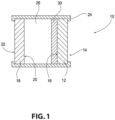
- the exemplary transparency 10 of Fig. 1 is in the form of a conventional insulating glass unit and includes a first ply 12 with a first major surface 14 (No. 1 surface) and an opposed second major surface 16 (No. 2 surface).
- the first major surface 14 faces the building exterior, i.e., is an outer major surface
- the second major surface 16 faces the interior of the building.
- the transparency 10 also includes a second ply 18 having an outer (first) major surface 20 (No. 3 surface) and an inner (second) major surface 22 (No. 4 surface) and spaced from the first ply 12. This numbering of the ply surfaces is in keeping with conventional practice in the fenestration art.
- the first and second plies 12, 18 can be connected together in any suitable manner, such as by being adhesively bonded to a conventional spacer frame 24.
- a gap or chamber 26 is formed between the two plies 12, 18.
- the chamber 26 can be filled with a selected atmosphere, such as air, or a non-reactive gas such as argon or krypton gas.
- a solar control coating 30 (or any of the other coatings described below) is formed over at least a portion of one of the plies 12, 18, such as, but not limited to, over at least a portion of the No. 2 surface 16 or at least a portion of the No. 3 surface 20. Although, the coating could also be on the No. 1 surface or the No. 4 surface, if desired. Examples of insulating glass units are found, for example, in U.S. Patent Nos. 4,193,236 ; 4,464,874 ; 5,088,258 ; and 5,106,663 .
- the plies 12, 18 of the transparency 10 can be of the same or different materials.
- the plies 12, 18 can include any desired material having any desired characteristics.
- one or more of the plies 12, 18 can be transparent or translucent to visible light.
- transparent is meant having visible light transmission of greater than 0% up to 100%.
- one or more of the plies 12, 18 can be translucent.
- translucent is meant allowing electromagnetic energy (e.g., visible light) to pass through but diffusing this energy such that objects on the side opposite the viewer are not clearly visible.
- suitable materials include, but are not limited to, plastic substrates (such as acrylic polymers, such as polyacrylates; polyalkylmethacrylates, such as polymethylmethacrylates, polyethylmethacrylates, polypropylmethacrylates, and the like; polyurethanes; polycarbonates; polyalkylterephthalates, such as polyethyleneterephthalate (PET), polypropyleneterephthalates, polybutyleneterephthalates, and the like; polysiloxane-containing polymers; or copolymers of any monomers for preparing these, or any mixtures thereof); ceramic substrates; glass substrates; or mixtures or combinations of any of the above.
- plastic substrates such as acrylic polymers, such as polyacrylates; polyalkylmethacrylates, such as polymethylmethacrylates, polyethylmethacrylates, polypropylmethacrylates, and the like; polyurethanes; polycarbonates; polyalkylterephthalates, such as polyethyleneterephthal
- one or more of the plies 12, 18 can include conventional soda-lime-silicate glass, borosilicate glass, or leaded glass.
- the glass can be clear glass.
- clear glass is meant non-tinted or non-colored glass.
- the glass can be tinted or otherwise colored glass.
- the glass can be annealed or heat-treated glass.
- heat treated means tempered or at least partially tempered.
- the glass can be of any type, such as conventional float glass, and can be of any composition having any optical properties, e.g., any value of visible transmission, ultraviolet transmission, infrared transmission, and/or total solar energy transmission.
- float glass glass formed by a conventional float process in which molten glass is deposited onto a molten metal bath and controllably cooled to form a float glass ribbon. Examples of float glass processes are disclosed in U.S. Patent Nos. 4,466,562 and 4,671,155 .
- the first and second plies 12, 18 can each be, for example, clear float glass or can be tinted or colored glass or one ply 12, 18 can be clear glass and the other ply 12, 18 colored glass.
- examples of glass suitable for the first ply 12 and/or second ply 18 are described in U.S. Patent Nos. 4,746,347 ; 4,792,536 ; 5,030,593 ; 5,030,594 ; 5,240,886 ; 5,385,872 ; and 5,393,593 .
- the first and second plies 12, 18 can be of any desired dimensions, e.g., length, width, shape, or thickness.
- the first and second plies can each be 1 mm to 10 mm thick, such as 1 mm to 8 mm thick, such as 2 mm to 8 mm, such as 3 mm to 7 mm, such as 5 mm to 7 mm, such as 6 mm thick.
- the solar control coating 30 of the invention is deposited over at least a portion of at least one major surface of one of the glass plies 12, 18. In the example shown in Fig. 1 , the coating 30 is formed over at least a portion of the inner surface 16 of the outboard glass ply 12.
- the term "solar control coating” refers to a coating comprised of one or more layers or films that affect the solar properties of the coated article, such as, but not limited to, the amount of solar radiation, for example, visible, infrared, or ultraviolet radiation, reflected from, absorbed by, or passing through the coated article; shading coefficient; emissivity, etc.
- the solar control coating 30 can block, absorb, or filter selected portions of the solar spectrum, such as, but not limited to, the IR, UV, and/or visible spectrums.
- the solar control coating 30 can be deposited by any conventional method, such as, but not limited to, conventional chemical vapor deposition (CVD) and/or physical vapor deposition (PVD) methods.
- CVD processes include spray pyrolysis.
- PVD processes include electron beam evaporation and vacuum sputtering (such as magnetron sputter vapor deposition (MSVD)).
- Other coating methods could also be used, such as, but not limited to, sol-gel deposition.
- the coating 30 can be deposited by MSVD. Examples of MSVD coating devices and methods will be well understood by one of ordinary skill in the art and are described, for example, in U.S. Patent Nos. 4,379,040 ; 4,861,669 ; 4,898,789 ; 4,898,790 ; 4,900,633 ; 4,920,006 ; 4,938,857 ; 5,328,768 ; and 5,492,750 .
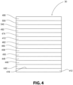
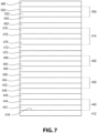
- This exemplary coating 30 includes a base layer or first dielectric layer 440 deposited over at least a portion of a major surface of a substrate (e.g., the No. 2 surface 416 of the first ply 12).
- the first dielectric layer 440 can be a single layer or can comprise more than one film of antireflective materials and/or dielectric materials, such as, but not limited to, metal oxides, oxides of metal alloys, nitrides, oxynitrides, or mixtures thereof.
- the first dielectric layer 440 can be transparent to visible light.
- suitable metal oxides or metal nitrides for the first dielectric layer 440 or any film therein include oxides, nitrides or oxynitrides of titanium, hafnium, zirconium, niobium, zinc, bismuth, lead, indium, tin, aluminum, silicon and mixtures thereof.
- the metal oxides can have small amounts of other materials, such as manganese in bismuth oxide, tin in indium oxide, etc.
- oxides of metal alloys or metal mixtures can be used, such as oxides containing zinc and tin (e.g., zinc stannate, defined below), oxides of indium-tin alloys, silicon nitrides, silicon aluminum nitrides, or aluminum nitrides.
- doped metal oxides such as antimony or indium doped tin oxides or nickel or boron doped silicon oxides, can be used.
- the first dielectric layer 440 can be a substantially single phase film, such as a metal alloy oxide film, e.g., zinc stannate, or can be a mixture of phases composed of zinc and tin oxides or can be composed of a plurality of films.
- the first dielectric layer 440 can comprise a multi-film structure having a first film 442, e.g., a metal alloy oxide film, deposited over at least a portion of a substrate (such as the inner major surface 16 of the first ply 12) and a second film 444, e.g., a metal oxide or oxide mixture film, deposited over the first film 442.
- the first film 442 can be a zinc/tin alloy oxide.
- zinc/tin alloy oxide is meant both true alloys and also mixtures of the oxides.
- the zinc/tin alloy oxide can be that obtained from magnetron sputtering vacuum deposition from a cathode of zinc and tin.
- One non-limiting cathode can comprise zinc and tin in proportions of 5 wt.% to 95 wt.% zinc and 95 wt.% to 5 wt.% tin, such as 10 wt.% to 90 wt.% zinc and 90 wt.% to 10 wt.% tin.
- suitable metal alloy oxide that can be present in the first film 442 is zinc stannate.
- zinc stannate is meant a composition of Zn X Sn 1-X O 2- x (Formula 1) where "x" varies in the range of greater than 0 to less than 1.
- x can be greater than 0 and can be any fraction or decimal between greater than 0 to less than 1.
- Formula 1 is Zn 2/3 Sn 1/3 O 4/3 , which is more commonly described as “Zn 2 SnO 4 ".
- a zinc stannate-containing film has one or more of the forms of Formula 1 in a predominant amount in the film.
- the second film 444 can be a metal oxide film, such as zinc oxide.
- the zinc oxide can be deposited from a zinc cathode that includes other materials to improve the sputtering characteristics of the cathode.
- the zinc cathode can include a small amount (e.g., up to 20 wt.%, up to 15 wt.%, up to 10 wt.%, or up to 5 wt.%) of tin to improve sputtering.
- the resultant zinc oxide film would include a small percentage of tin oxide, e.g., up to 10 wt.% tin oxide, e.g., up to 5 wt.% tin oxide.
- a coating layer deposited from a zinc cathode having up to 10 wt.% tin (added to enhance the conductivity of the cathode) is referred to herein as "a zinc oxide film" even though a small amount of tin may be present.
- the small amount of tin in the cathode e.g., less than or equal to 10 wt.%, such as less than or equal to 5 wt.% is believed to form tin oxide in the predominantly zinc oxide second film 44.
- a first metallic layer 446 is deposited over the first dielectric layer 440.
- the first metallic layer 446 can include a reflective metal, such as, but not limited to, metallic gold, copper, palladium, aluminum, silver, or mixtures, alloys, or combinations thereof.
- the reflective metal is silver or copper.
- the first metallic layer 446 has contains silver and copper.
- the first metallic layer 446 can be a continuous layer.
- the first metallic layer 446 can be a discontinuous layer.
- the first metallic layer 446 has a thickness in the range of 60 to 150 ⁇ ,
- the first metallic layer 446 can have a thickness of preferably less than 125 ⁇ , more preferably less than 100 ⁇ ; and/or preferably greater than 65 ⁇ ; more preferably greater than 70 ⁇ .
- the first metallic layer 446 has a thickness of 78 ⁇ to 121 ⁇ .
- the first metallic layer 446 has a thickness of 70 ⁇ to 99 ⁇ .
- a first primer layer 448 is located over the first metallic layer 446.
- the first primer layer 448 can be a single film or a multiple film layer.
- the first primer layer 448 can include an oxygen-capturing material that can be sacrificial during the deposition process to prevent degradation or oxidation of the first metallic layer 446 during the sputtering process or subsequent heating processes.
- the first primer layer 448 can also absorb at least a portion of electromagnetic radiation, such as visible light, passing through the coating 30.
- first primer layer 448 examples include titanium, silicon, silicon dioxide, silicon nitride, silicon oxynitride, nickel-chrome alloys (such as Inconel), zirconium, aluminum, alloys of silicon and aluminum, alloys containing cobalt and chromium (e.g., Stellite ® ), and mixtures thereof.
- the first primer layer 448 can be titanium or an alloy or mixture of titanium and aluminum.
- a second dielectric layer 450 is located over the first primer layer 448.
- the second dielectric layer 450 can comprise one or more metal oxide or metal alloy oxide-containing films, such as those described above with respect to the first dielectric layer 440.
- the second dielectric layer 450 can include a first film 452, e.g., a zinc oxide film, deposited over first metallic layer 446 or the optional first primer film 448 and a second film 454, e.g., a zinc stannate (Zn 2 SnO 4 ) film, deposited over the first film 452.
- An optional third film 456, e.g., a second zinc oxide film can be deposited over the second film.
- a second metallic layer 458 is located over the second dielectric layer 450 (e.g., over the second zinc oxide film 456, if present, or over the zinc stannate film 454 if not).
- the metallic material can be metallic gold, copper, palladium, aluminum, silver, or mixtures, alloys, or combinations thereof. It can be applied as a continuous layer or as a discontinuous layer such that isolated regions or islands of the material are formed rather than a continuous layer of the material.
- the second metallic layer 458 can have a thickness that is thicker than the first metallic layer 446.
- the second metallic layer 458 has a thickness in the range of 70 to 250 ⁇ , .
- the second metallic layer 458 can have a thickness of preferably at least 100 ⁇ , more preferably at least 125 ⁇ , most preferably at least 128 ⁇ ; and/or preferably at most 225 ⁇ , more preferably at most 200 ⁇ , most preferably at most 191 ⁇ .
- a second primer layer 460 is deposited over the second metallic layer 458.
- the second primer layer 460 can be as described above with respect to the first primer layer 448.
- the second primer layer 460 can be titanium. Any of the primer layers can be sputtered in a non-reactive atmosphere, such a low oxygen or oxygen free atmosphere. Then, the coated article could be subjected to further processing, such as the deposition of further oxide layers in an oxygen containing atmosphere. During this further deposition, the primer would oxidize.
- a third dielectric layer 462 is deposited over the second primer film 460.
- the third dielectric layer 462 can also include one or more metal oxide or metal alloy oxide-containing layers, such as discussed above with respect to the first and second dielectric layers 440, 450.
- the third dielectric layer 462 can include a first film 464, e.g., a zinc oxide film, a second film 466, e.g., a zinc stannate film deposited over the first film 464.
- An optional third film 468 e.g., a second zinc oxide layer, can be deposited over the second film.
- a third metallic layer 470 is deposited over the third dielectric layer 462.
- the third metallic layer 470 can be of any of the materials discussed above with respect to the first metallic layer 446.
- the third metallic layer 470 includes silver, copper, or silver and copper.
- the third metallic layer 470 is a discontinuous layer.
- the third metallic layer 470 is thinner that the second metallic layer 458.
- the third metallic layer has a thickness in the range of 10 to 25 ⁇ .
- a third primer layer 472 is located over the third metallic layer 470.
- the third primer layer 472 can be as described above with respect to the first or second primer layers 448 or 460.
- a fourth dielectric layer 474 is located over the third primer layer 472.
- the fourth dielectric layer 474 can be comprised of one or more metal oxide or metal alloy oxide-containing layers, such as those discussed above with respect to the first, second, or third dielectric layers 440, 450, 462.
- the fourth dielectric layer 474 is a multi-film layer having a first film 476 deposited over the third primer layer 472, and a second film 478 deposited over the first film 476.
- An optional third film 479 can be deposited over the second film.
- a fourth metallic layer 492 is located over the fourth dielectric layer 474.
- the fourth metallic layer 492 can include a reflective metal, such as, but not limited to, metallic gold, copper, palladium, aluminum, silver, or mixtures, alloys, or combinations thereof.
- the reflective metal is silver, copper or a combination of silver and copper.
- the fourth metallic layer 492 has contains silver and copper.
- the fourth metallic layer 492 can be a continuous layer or a discontinuous layer.
- the fourth metallic layer 492 can be thicker than the first metallic layer 446.
- the fourth metallic layer 492 is thicker than the third metallic layer 470.
- the fourth metallic layer has a thickness in the range of 60 to 275 ⁇ .
- the fourth metallic layer can have a thickness of at least 100 ⁇ , preferably at least 150 ⁇ , more preferably at least 175 ⁇ , most preferably at least 181 ⁇ ; and/or preferably at most 250 ⁇ , more preferably at most 240 ⁇ .
- a fourth primer layer 540 is deposited over the fourth metallic layer 492.
- the fourth primer layer 540 can be as described above with respect to the first primer layer 448, second primer layer 460 or third primer layer 472.
- the fourth primer layer 540 can be titanium.
- a fifth dielectric layer 550 is located over the fourth primer layer 540.
- the fifth dielectric layer 550 can be comprised of one or more metal oxide or metal alloy oxide-containing layers, such as those discussed above with respect to the first, second, third or fourth dielectric layers 440, 450, 462, 474.
- the fifth dielectric layer 550 is a multi-film layer having a first film 502 deposited over the fourth primer layer 540, and a second film 504 deposited over the first film 502.
- the fifth dielectric layer 550 has first film 502 and a second film 504.
- the first film comprises zinc oxide.
- the second film comprises silicon nitride.
- the fifth dielectric layer 550 has a first film 502, a second film 504 and a third film (not shown).
- the first film 502 comprises zinc oxide or zinc stannate.
- the second film 504 comprises zinc stannate, silicon oxide, or silicon oxynitride.
- the third film comprises silicon nitride. Silicon oxide, silicon oxynitrides and silicon nitride can contain aluminum, such as aluminum oxide or aluminum nitride, in amounts of up to 5 weight percent, up to 10 weight percent, up to 15 weight percent or up to 20 weight percent.
- the second film 504 and the third film are a gradient layer from silicon oxide or silicon oxynitrides to silicon nitride.
- An overcoat 480 is located over the fifth dielectric layer 550.
- the overcoat 480 can help protect the underlying coating layers from mechanical and chemical attack.
- the overcoat 480 can be, for example, a metal oxide or metal nitride layer.
- the overcoat 480 can be titania, or a mixture of titania and alumina.
- Other materials useful for the overcoat include other oxides, such as silica, alumina, or a mixture of silica and alumina.
- the transparency has a visible light transmittance of greater than 20%, such as greater than 30%, such as greater than 34%.
- the transparency has a solar heat gain coefficient (SHGC) of less than 0.3, such as less than 0.27, such as less than 0.25, such equal to or as less than 0.22, such as less than 0.20, such as less than 0.19; and/or at least 0.10; at least 0.12; at least 0.15; or at least 0.17.
- the transparency has a light to solar gain ratio (LSG) of at least 1.7, at least 1.75, at least 1.8, or at least 1.85; and/or at most 2.25; at most 2.15; at most 2.10; or at most 2.06.
- the coated article can have a total thickness of all the metallic layers (e.g. total thickness being the combine thickness of first, second, third and fourth metallic layers). This total thickness can be in the range of 200 ⁇ to 750 ⁇ , preferably 225 ⁇ to 650 ⁇ , more preferably 250 ⁇ to 600 ⁇ , most preferably 252 ⁇ to 582 ⁇ .
- the coated article can have a total thickness of all of the metallic layers which are continuous layers (i.e. excluding the thickness of the discontinuous layer(s)).
- the total thickness of all of the continuous layers can be in the range of 150 ⁇ to 750 ⁇ , preferably 200 ⁇ to 650 ⁇ , more preferably 225 ⁇ to 575 ⁇ , most preferably 237 ⁇ to 563 ⁇ .
- the coated article can have a single discontinuous metallic layer wherein all other metallic layers are continuous metallic layers.
- a primer such as any of the primers described above, may be positioned over and in direct contact with any of the metallic layers.
- the primer may be a mixture of titanium and aluminum.
- the method includes providing a substrate.
- a first dielectric layer is applied over at least a portion of the substrate.
- a first metallic layer is applied over at least a portion of the first dielectric layer.
- a second dielectric layer is applied over at least a portion of the first metallic layer.
- a second metallic layer is applied over at least a portion of the second dielectric layer.
- a third dielectric layer is applied over at least a portion of the second metallic layer.
- a third metallic layer is applied over at least a portion of the third dielectric layer.
- a fourth dielectric layer is applied over at least a portion of the third metallic layer.
- a fourth metallic layer is applied over at least a portion of the fourth dielectric layer.
- a fifth dielectric layer is applied over at least a portion of the fourth metallic layer.
- the third metallic layer is a discontinuous layer.
- a protective overcoat is applied over the fifth dielectric layer.
- a primer is applied over the first metallic layer, second metallic layer, third metallic layer and fourth metallic layer.
- the method includes providing a first ply having a number 1 surface and a number 2 surface, providing a second ply having a number 3 surface and a number 4 surface. Either the number 2 surface of the first ply or the number 3 surface of the second ply have the coating described herein.
- the first ply and the second ply are assembled in a manner so that the number 2 surface faces the number three surface and that there is a space between the number 2 surface and the number 3 surface.
- the space is filled with a gas.
- the gas can be air or argon.
- the discontinuous metallic layer is the third metallic layer.
- the coating has thickness for each layer as described in Table 1, or for each film as described in Table 2.
- the third dielectric layer is thicker than the first dielectric layer, the second dielectric layer, the fourth dielectric layer and/or the fifth dielectric layer.
- the third dielectric layer also comprises the third film.
- Layer Thickness, Discontinuous Metallic layer is the Third Metallic layer Layer Range ( ⁇ ) Preferred ( ⁇ ) More Preferred ( ⁇ ) 1 st Dielectric 300-525 325-475 353-446 1 st Metallic 60-150 70-125 70-99 or 78-121 1 st Primer 15-45 20-40 25-36 2 nd Dielectric 400-1000 475-900 504-824 2 nd Metallic 70-250 75-200 79-191 2 nd Primer 15-45 20-40 25-36 3 rd Dielectric 100-600 150-450 199-412 3 rd Metallic 10-25 12-22 15-19 3 rd Primer 15-45 17-40 20-36 4 th Dielectric 250-700 300-650 334-603 4 th Metallic 60-275 75-250 80-240 4 th Primer 15-45 20-40 25-36 5 th Dielectric 175-450 225-400 260-340 Overcoat 30-60 35-55 40-50 Table 2: Film Thickness, Discontinuous Metallic Layer Is The Third Metallic Layer Layer Range ( ⁇
- Examples 1-4 were prepared by coating glass with the coating stacks described in Table 5. Table 5: Examples 1-4 Example 1 Example 2 Example 3 Example 4 Material Thickness ( ⁇ ) Thickness ( ⁇ ) Thickness ( ⁇ ) Thickness ( ⁇ ) Glass Zn 2 SnO 4 312 301 262 307 ZnO 109 109 91 109 Ag 78 81 121 78 Ti 35 35 35 35 ZnO 63 63 71 63 Zn 2 SnO 4 524 551 463 490 ZnO 81 85 95 84 Ag 182 191 128 154 Ti 35 36 36 36 ZnO 99 97 105 99 Zn 2 SnO 4 296 315 292 200 Ag 18.8 17.1 15.75 17 Zn 2 SnO 4 296 300 246 340 ZnO 103 102 88 103 Ag 188 197 240 181 Ti 28 28 28 28 ZnO 90 90 107 90 Zn 2 SnO 4 172 170 205 170 TiO 2 44 44 44 44 44 44 44 44 44 44 44
- Example 1 the LTA was 34.0, the SHGC was 0.183 and the LSG was 1.86.
- Example 2 the LTA was 34.3, the SHGC was 0.178 and the LSG was 1.93.
- Example 3 the LTA was 37.3, the SHGC was 0.182 and the LSG was 2.05.
- Example 4 the LTA was 40.1, the SHGC was 0.22, and the LSG was 1.82.
- Examples 5-7 were prepared by coating glass with the coating stacks described in Table 6. Table 6: Examples 5-7 Example 5 Example 6 Example 7 Material Thickness (nm) Thickness (nm) Thickness (nm) Glass Zn 2 SnO 4 30.7 33.7 31.7 ZnO 10.9 10.9 10.9 Ag 11.2 10.7 10.7 Ti 3.5 3.5 3.5 ZnO 6.3 6.3 6.3 Zn 2 SnO 4 42.0 36.0 68.0 ZnO 8.1 8.1 Ag 12.4 7.9 16.4 Ti 3.6 3.6 3.6 ZnO 9.9 9.9 9.9 Zn 2 SnO 4 20.0 10.0 20.0 Ag 1.5 1.9 1.7 Ti 2.0 3.0 3.5 Zn 2 SnO 4 34.0 50.0 35.0 ZnO 10.3 10.3 10.3 Ag 23.8 19.5 10.0 Ti 2.8 2.8 2.8 2.8 2.8 2.8 2.8 2.8 2.8 2.8 2.8 2.8 2.8 2.8 2.8 2.8 2.8 2.8 2.8 2.8 2.8 2.8 2.8 2.8 2.8 2.8 2.8 2.8 2.8
- Example 8 (not according to the invention) was prepared by coating glass with the coating stack described in Table 7. Table 7: Example 8 Example 8 Material Thickness (nm) Glass Zn 2 SnO 4 31.7 ZnO 10.9 Ag 13.2 Ti 3.5 ZnO 9.0 Zn 2 SnO 4 33.0 Ag 1.7 Zn 2 SnO 4 24.0 ZnO 8.0 Ag 16.4 Ti 3.6 ZnO 9.9 Zn 2 SnO 4 57.0 ZnO 5.4 Ag 8.0 Ti 2.8 ZnO 9.0 Zn 2 SnO 4 21.0 TiO 2 4.4
Description
- This invention relates generally to coated articles having certain solar control coatings with four metallic layers.
- Solar control coatings are known in the fields of architectural and vehicle transparencies. These solar control coatings block or filter selected ranges of electromagnetic radiation, such as in the range of solar infrared or solar ultraviolet radiation, to reduce the amount of solar energy entering the vehicle or building. This reduction of solar energy transmittance helps reduce the load on the cooling units of the vehicle or building.
-
WO 2016/126758 A1 relates to a solar control coating including at least four phase adjustment layers and at least four metal functional layers, whereby at least one of the metal functional layers can be a subcritical layer. - The present invention relates to a coated article as defined in appended independent claim 1. Specific variants of the coated article of the present invention are presented in the appended dependent claims. A coated article of the invention includes a coating as defined in appended claim 1 over at least a portion of a substrate. The coating includes at least three continuous metallic layers and at least one discontinuous metallic layer. The discontinuous metallic layer increases the visible light absorption of the coating and, in combination with dielectric layers of appropriate thickness, can also provide the coated article with asymmetrical reflectance.
- A coating of the invention includes a coating over at least a portion of a substrate, whereby the coating includes at least four metallic layers alternating with at least five dielectric layers wherein the third metallic layer is a discontinuous metallic layer having discontinuous metal regions.
- A coated article of the invention is defined in appended claim 1 and includes a substrate and a coating formed over at least a portion of the substrate. The coating inter alia includes a first dielectric layer formed over at least a portion of the substrate; a first metallic layer formed over at least a portion of the first dielectric layer; a first primer layer over at least a portion of the first metallic layer; a second dielectric layer formed over at least a portion of the first primer layer; a second metallic layer formed over at least a portion of the second dielectric layer; a second primer layer over at least a portion of the second metallic layer; a third dielectric layer formed over at least a portion of the second primer layer; a third metallic layer formed over at least a portion of the third dielectric layer; a third primer layer over at least a portion of the third metallic layer; a fourth dielectric layer formed over at least a portion of the third primer layer; a fourth metallic layer formed over at least a portion of the fourth dielectric layer; a fourth primer layer over at least a portion of the fourth metallic layer; a fifth dielectric layer formed over at least a portion of the fourth primer layer; and a protective layer formed over at least a portion of the fifth dielectric layer, whereby the third metallic layer is a discontinuous layer.
- Further disclosed herein is a method of making a coated article of the invention including providing a substrate. A first dielectric layer is applied over at least a portion of the substrate. A first metallic layer is applied over at least a portion of the first dielectric layer. A first primer layer is applied over at least a portion of the first metallic layer. A second dielectric layer is applied over at least a portion of the first primer layer. A second metallic layer is applied over at least a portion of the second dielectric layer. A second primer layer is applied over at least a portion of the second metallic layer. A third dielectric layer is applied over at least a portion of the second primer layer. A third metallic layer is applied over at least a portion of the third dielectric layer. A third primer layer is applied over at least a portion of the third metallic layer. A fourth dielectric layer is applied over at least a portion of the third primer layer. A fourth metallic layer is applied over at least a portion of the fourth dielectric layer. A fourth primer layer is applied over at least a portion of the fourth metallic layer. A fifth dielectric layer is applied over at least a portion of the fourth primer layer. An overcoat is applied over at least a portion of the firth dielectric layer. The third metallic layer is a discontinuous layer having discontinuous metallic regions.
- The coated article of the invention can for example be used in an architectural transparency. The transparency has a first ply having a number 1 surface and a number 2 surface and a second ply having a number 3 surface and a number 4 surface. A coating, as described herein, is positioned over at least a portion of the number 2 surface or the number 3 surface.
- Also disclosed herein is a method of making an architectural transparency as mentioned above. The method includes providing a first ply having a number 1 surface and a number 2 surface, and a second ply having a number 3 surface and a number 4 surface. Either the number 2 surface of the first ply or the number 3 surface of the second ply have a coating as described herein. The first ply and the second ply are assembled so that the number 2 surface faces the number three surface and that there is a space between the number 2 surface and the number 3 surface. The space is filled with a gas.
- The invention will be described with reference to the following drawing figures wherein like reference numbers identify like parts throughout.
-
Fig. 1 is a side view (not to scale) of an insulating glass unit (IGU) having a coating of the invention; -
Fig. 2 is a side, sectional view (not to scale) of a subcritical metal layer with a primer layer; -
Fig. 3 is a side, sectional view (not to scale) of a further coating of the invention. -
Fig. 4 is a sectional view (not to scale) of a coating of the invention. -
Fig. 5 is a sectional view (not to scale) of the coating of the invention. -
Fig. 6 is a sectional view (not to scale) of the coating of the invention. -
Fig. 7 is a sectional view (not to scale) of the coating of the invention. - As used herein, spatial or directional terms, such as "left", "right", "inner", "outer", "above", "below", and the like, relate to the invention as it is shown in the drawing figures. However, it is to be understood that the invention can assume various alternative orientations and, accordingly, such terms are not to be considered as limiting. Further, as used herein, all numbers expressing dimensions, physical characteristics, processing parameters, quantities of ingredients, reaction conditions, and the like, used in the specification and claims are to be understood as being modified in all instances by the term "about". Accordingly, unless indicated to the contrary, the numerical values set forth in the following specification and claims may vary depending upon the desired properties sought to be obtained by the present invention. At the very least, and not as an attempt to limit the application of the doctrine of equivalents to the scope of the claims, each numerical value should at least be construed in light of the number of reported significant digits and by applying ordinary rounding techniques. Moreover, all ranges disclosed herein are to be understood to encompass the beginning and ending range values and any and all subranges subsumed therein. For example, a stated range of "1 to 10" should be considered to include any and all subranges between (and inclusive of) the minimum value of 1 and the maximum value of 10; that is, all subranges beginning with a minimum value of 1 or more and ending with a maximum value of 10 or less, e.g., 1 to 3.3, 4.7 to 7.5, 5.5 to 10, and the like. Further, as used herein, the terms "formed over", "deposited over", or "provided over" mean formed, deposited, or provided on but not necessarily in contact with the surface. For example, a coating layer "formed over" a substrate does not preclude the presence of one or more other coating layers or films of the same or different composition located between the formed coating layer and the substrate. The terms "visible region" or "visible light" refer to electromagnetic radiation having a wavelength in the range of 380 nm to 800 nm. The terms "infrared region" or "infrared radiation" refer to electromagnetic radiation having a wavelength in the range of greater than 800 nm to 100,000 nm. The terms "ultraviolet region" or "ultraviolet radiation" mean electromagnetic energy having a wavelength in the range of 300 nm to less than 380 nm. As used herein, the term "film" refers to a coating region of a desired or selected coating composition. A "layer" can comprise one or more "films", and a "coating" or "coating stack" can comprise one or more "layers". The term "asymmetrical reflectivity" means that the visible light reflectance of the coating from one side is different than that of the coating from the opposite side. The term "critical thickness" means a thickness above which a coating material forms a continuous, uninterrupted layer and below which the coating material forms discontinuous regions or islands of the coating material rather than a continuous layer. The term "subcritical thickness" means a thickness below the critical thickness such that the coating material forms isolated, non-connected regions of the coating material. The term "islanded" means that the coating material is not a continuous layer but, rather, that the material is deposited to form isolated regions or islands.
- For purposes of the following discussion, the invention will be discussed with reference to use with an architectural transparency, such as, but not limited to, an insulating glass unit (IGU). As used herein, the term "architectural transparency" refers to any transparency located on a building, such as, but not limited to, windows and sky lights. However, it is to be understood that the invention is not limited to use with such architectural transparencies but could be practiced with transparencies in any desired field, such as, but not limited to, laminated or non-laminated residential and/or commercial windows, insulating glass units, and/or transparencies for land, air, space, above water and underwater vehicles. Therefore, it is to be understood that the specifically disclosed exemplary embodiments are presented simply to explain the general concepts of the invention, and that the invention is not limited to these specific exemplary embodiments. Additionally, while a typical "transparency" can have sufficient visible light transmission such that materials can be viewed through the transparency, in the practice of the invention, the "transparency" need not be transparent to visible light but may be translucent or opaque.
- A
non-limiting transparency 10 incorporating features of the invention is illustrated inFig. 1 . Thetransparency 10 can have any desired visible light, infrared radiation, or ultraviolet radiation transmission and/or reflection. For example, thetransparency 10 can have a visible light transmission of any desired amount, e.g., greater than 0% up to 100%. - The
exemplary transparency 10 ofFig. 1 is in the form of a conventional insulating glass unit and includes afirst ply 12 with a first major surface 14 (No. 1 surface) and an opposed second major surface 16 (No. 2 surface). In the illustrated non-limiting embodiment, the firstmajor surface 14 faces the building exterior, i.e., is an outer major surface, and the secondmajor surface 16 faces the interior of the building. Thetransparency 10 also includes asecond ply 18 having an outer (first) major surface 20 (No. 3 surface) and an inner (second) major surface 22 (No. 4 surface) and spaced from thefirst ply 12. This numbering of the ply surfaces is in keeping with conventional practice in the fenestration art. The first andsecond plies conventional spacer frame 24. A gap or chamber 26 is formed between the twoplies plies surface 16 or at least a portion of the No. 3surface 20. Although, the coating could also be on the No. 1 surface or the No. 4 surface, if desired. Examples of insulating glass units are found, for example, inU.S. Patent Nos. 4,193,236 ;4,464,874 ;5,088,258 ; and5,106,663 . - In the broad practice of the invention, the
plies transparency 10 can be of the same or different materials. Theplies plies plies plies U.S. Patent Nos. 4,466,562 and4,671,155 . - The first and
second plies ply other ply first ply 12 and/orsecond ply 18 are described inU.S. Patent Nos. 4,746,347 ;4,792,536 ;5,030,593 ;5,030,594 ;5,240,886 ;5,385,872 ; and5,393,593 . The first andsecond plies - The
solar control coating 30 of the invention is deposited over at least a portion of at least one major surface of one of the glass plies 12, 18. In the example shown inFig. 1 , thecoating 30 is formed over at least a portion of theinner surface 16 of theoutboard glass ply 12. As used herein, the term "solar control coating" refers to a coating comprised of one or more layers or films that affect the solar properties of the coated article, such as, but not limited to, the amount of solar radiation, for example, visible, infrared, or ultraviolet radiation, reflected from, absorbed by, or passing through the coated article; shading coefficient; emissivity, etc. Thesolar control coating 30 can block, absorb, or filter selected portions of the solar spectrum, such as, but not limited to, the IR, UV, and/or visible spectrums. - The
solar control coating 30 can be deposited by any conventional method, such as, but not limited to, conventional chemical vapor deposition (CVD) and/or physical vapor deposition (PVD) methods. Examples of CVD processes include spray pyrolysis. Examples of PVD processes include electron beam evaporation and vacuum sputtering (such as magnetron sputter vapor deposition (MSVD)). Other coating methods could also be used, such as, but not limited to, sol-gel deposition. In one non-limiting embodiment, thecoating 30 can be deposited by MSVD. Examples of MSVD coating devices and methods will be well understood by one of ordinary skill in the art and are described, for example, inU.S. Patent Nos. 4,379,040 ;4,861,669 ;4,898,789 ;4,898,790 ;4,900,633 ;4,920,006 ;4,938,857 ;5,328,768 ; and5,492,750 . - An exemplary non-limiting
solar control coating 30 of the invention is shown inFig. 4 . Thisexemplary coating 30 includes a base layer or firstdielectric layer 440 deposited over at least a portion of a major surface of a substrate (e.g., the No. 2surface 416 of the first ply 12). Thefirst dielectric layer 440 can be a single layer or can comprise more than one film of antireflective materials and/or dielectric materials, such as, but not limited to, metal oxides, oxides of metal alloys, nitrides, oxynitrides, or mixtures thereof. Thefirst dielectric layer 440 can be transparent to visible light. Examples of suitable metal oxides or metal nitrides for thefirst dielectric layer 440 or any film therein include oxides, nitrides or oxynitrides of titanium, hafnium, zirconium, niobium, zinc, bismuth, lead, indium, tin, aluminum, silicon and mixtures thereof. The metal oxides can have small amounts of other materials, such as manganese in bismuth oxide, tin in indium oxide, etc. Additionally, oxides of metal alloys or metal mixtures can be used, such as oxides containing zinc and tin (e.g., zinc stannate, defined below), oxides of indium-tin alloys, silicon nitrides, silicon aluminum nitrides, or aluminum nitrides. Further, doped metal oxides, such as antimony or indium doped tin oxides or nickel or boron doped silicon oxides, can be used. Thefirst dielectric layer 440 can be a substantially single phase film, such as a metal alloy oxide film, e.g., zinc stannate, or can be a mixture of phases composed of zinc and tin oxides or can be composed of a plurality of films. - As shown in
Fig. 5 , thefirst dielectric layer 440 can comprise a multi-film structure having afirst film 442, e.g., a metal alloy oxide film, deposited over at least a portion of a substrate (such as the innermajor surface 16 of the first ply 12) and asecond film 444, e.g., a metal oxide or oxide mixture film, deposited over thefirst film 442. In one non-limiting embodiment, thefirst film 442 can be a zinc/tin alloy oxide. By "zinc/tin alloy oxide" is meant both true alloys and also mixtures of the oxides. The zinc/tin alloy oxide can be that obtained from magnetron sputtering vacuum deposition from a cathode of zinc and tin. One non-limiting cathode can comprise zinc and tin in proportions of 5 wt.% to 95 wt.% zinc and 95 wt.% to 5 wt.% tin, such as 10 wt.% to 90 wt.% zinc and 90 wt.% to 10 wt.% tin. However, other ratios of zinc to tin could also be used. One suitable metal alloy oxide that can be present in thefirst film 442 is zinc stannate. By "zinc stannate" is meant a composition of ZnXSn1-XO2-x (Formula 1) where "x" varies in the range of greater than 0 to less than 1. For instance, "x" can be greater than 0 and can be any fraction or decimal between greater than 0 to less than 1. For example, where x = 2/3, Formula 1 is Zn2/3Sn1/3O4/3, which is more commonly described as "Zn2SnO4". A zinc stannate-containing film has one or more of the forms of Formula 1 in a predominant amount in the film. - The
second film 444 can be a metal oxide film, such as zinc oxide. The zinc oxide can be deposited from a zinc cathode that includes other materials to improve the sputtering characteristics of the cathode. For example, the zinc cathode can include a small amount (e.g., up to 20 wt.%, up to 15 wt.%, up to 10 wt.%, or up to 5 wt.%) of tin to improve sputtering. In which case, the resultant zinc oxide film would include a small percentage of tin oxide, e.g., up to 10 wt.% tin oxide, e.g., up to 5 wt.% tin oxide. A coating layer deposited from a zinc cathode having up to 10 wt.% tin (added to enhance the conductivity of the cathode) is referred to herein as "a zinc oxide film" even though a small amount of tin may be present. The small amount of tin in the cathode (e.g., less than or equal to 10 wt.%, such as less than or equal to 5 wt.%) is believed to form tin oxide in the predominantly zinc oxide second film 44. - A first
metallic layer 446 is deposited over thefirst dielectric layer 440. The firstmetallic layer 446 can include a reflective metal, such as, but not limited to, metallic gold, copper, palladium, aluminum, silver, or mixtures, alloys, or combinations thereof. In one embodiment, the reflective metal is silver or copper. In another embodiment, the firstmetallic layer 446 has contains silver and copper. The firstmetallic layer 446 can be a continuous layer. Alternatively, the firstmetallic layer 446 can be a discontinuous layer. The firstmetallic layer 446 has a thickness in the range of 60 to 150 Å, The firstmetallic layer 446 can have a thickness of preferably less than 125 Å, more preferably less than 100 Å; and/or preferably greater than 65 Å; more preferably greater than 70 Å. In one embodiment, the firstmetallic layer 446 has a thickness of 78 Å to 121 Å. In another embodiment, the firstmetallic layer 446 has a thickness of 70 Å to 99 Å. - A
first primer layer 448 is located over the firstmetallic layer 446. Thefirst primer layer 448 can be a single film or a multiple film layer. Thefirst primer layer 448 can include an oxygen-capturing material that can be sacrificial during the deposition process to prevent degradation or oxidation of the firstmetallic layer 446 during the sputtering process or subsequent heating processes. Thefirst primer layer 448 can also absorb at least a portion of electromagnetic radiation, such as visible light, passing through thecoating 30. Examples of materials useful for thefirst primer layer 448 include titanium, silicon, silicon dioxide, silicon nitride, silicon oxynitride, nickel-chrome alloys (such as Inconel), zirconium, aluminum, alloys of silicon and aluminum, alloys containing cobalt and chromium (e.g., Stellite®), and mixtures thereof. For example, thefirst primer layer 448 can be titanium or an alloy or mixture of titanium and aluminum. - A
second dielectric layer 450 is located over thefirst primer layer 448. Thesecond dielectric layer 450 can comprise one or more metal oxide or metal alloy oxide-containing films, such as those described above with respect to thefirst dielectric layer 440. With reference toFig. 5 , for example, thesecond dielectric layer 450 can include afirst film 452, e.g., a zinc oxide film, deposited over firstmetallic layer 446 or the optionalfirst primer film 448 and asecond film 454, e.g., a zinc stannate (Zn2SnO4) film, deposited over thefirst film 452. An optionalthird film 456, e.g., a second zinc oxide film, can be deposited over the second film. - A second
metallic layer 458 is located over the second dielectric layer 450 (e.g., over the secondzinc oxide film 456, if present, or over thezinc stannate film 454 if not). The metallic material can be metallic gold, copper, palladium, aluminum, silver, or mixtures, alloys, or combinations thereof. It can be applied as a continuous layer or as a discontinuous layer such that isolated regions or islands of the material are formed rather than a continuous layer of the material. The secondmetallic layer 458 can have a thickness that is thicker than the firstmetallic layer 446. The secondmetallic layer 458 has a thickness in the range of 70 to 250 Å, . The secondmetallic layer 458 can have a thickness of preferably at least 100 Å, more preferably at least 125 Å, most preferably at least 128 Å; and/or preferably at most 225 Å, more preferably at most 200 Å, most preferably at most 191 Å. - A
second primer layer 460 is deposited over the secondmetallic layer 458. Thesecond primer layer 460 can be as described above with respect to thefirst primer layer 448. In one example, thesecond primer layer 460 can be titanium. Any of the primer layers can be sputtered in a non-reactive atmosphere, such a low oxygen or oxygen free atmosphere. Then, the coated article could be subjected to further processing, such as the deposition of further oxide layers in an oxygen containing atmosphere. During this further deposition, the primer would oxidize. - A
third dielectric layer 462 is deposited over thesecond primer film 460. The thirddielectric layer 462 can also include one or more metal oxide or metal alloy oxide-containing layers, such as discussed above with respect to the first and seconddielectric layers dielectric layer 462 can include afirst film 464, e.g., a zinc oxide film, asecond film 466, e.g., a zinc stannate film deposited over thefirst film 464. An optionalthird film 468, e.g., a second zinc oxide layer, can be deposited over the second film. - A third
metallic layer 470 is deposited over the thirddielectric layer 462. The thirdmetallic layer 470 can be of any of the materials discussed above with respect to the firstmetallic layer 446. In one non-limiting example, the thirdmetallic layer 470 includes silver, copper, or silver and copper. The thirdmetallic layer 470 is a discontinuous layer. The thirdmetallic layer 470 is thinner that the secondmetallic layer 458. The third metallic layer has a thickness in the range of 10 to 25 Å. - A
third primer layer 472 is located over the thirdmetallic layer 470. Thethird primer layer 472 can be as described above with respect to the first or second primer layers 448 or 460. - A
fourth dielectric layer 474 is located over thethird primer layer 472. Thefourth dielectric layer 474 can be comprised of one or more metal oxide or metal alloy oxide-containing layers, such as those discussed above with respect to the first, second, or thirddielectric layers fourth dielectric layer 474 is a multi-film layer having afirst film 476 deposited over thethird primer layer 472, and asecond film 478 deposited over thefirst film 476. An optionalthird film 479 can be deposited over the second film. - A fourth
metallic layer 492 is located over thefourth dielectric layer 474. The fourthmetallic layer 492 can include a reflective metal, such as, but not limited to, metallic gold, copper, palladium, aluminum, silver, or mixtures, alloys, or combinations thereof. In one embodiment, the reflective metal is silver, copper or a combination of silver and copper. In one embodiment, the fourthmetallic layer 492 has contains silver and copper. The fourthmetallic layer 492 can be a continuous layer or a discontinuous layer. The fourthmetallic layer 492 can be thicker than the firstmetallic layer 446. The fourthmetallic layer 492 is thicker than the thirdmetallic layer 470. The fourth metallic layer has a thickness in the range of 60 to 275 Å. The fourth metallic layer can have a thickness of at least 100 Å, preferably at least 150 Å, more preferably at least 175 Å, most preferably at least 181 Å; and/or preferably at most 250 Å, more preferably at most 240 Å. - A
fourth primer layer 540 is deposited over the fourthmetallic layer 492. Thefourth primer layer 540 can be as described above with respect to thefirst primer layer 448,second primer layer 460 orthird primer layer 472. In one example, thefourth primer layer 540 can be titanium. - A
fifth dielectric layer 550 is located over thefourth primer layer 540. Thefifth dielectric layer 550 can be comprised of one or more metal oxide or metal alloy oxide-containing layers, such as those discussed above with respect to the first, second, third or fourthdielectric layers fifth dielectric layer 550 is a multi-film layer having afirst film 502 deposited over thefourth primer layer 540, and asecond film 504 deposited over thefirst film 502. - In another non-limiting example, the
fifth dielectric layer 550 hasfirst film 502 and asecond film 504. The first film comprises zinc oxide. The second film comprises silicon nitride. - In another non-limiting example, the
fifth dielectric layer 550 has afirst film 502, asecond film 504 and a third film (not shown). Thefirst film 502 comprises zinc oxide or zinc stannate. Thesecond film 504 comprises zinc stannate, silicon oxide, or silicon oxynitride. The third film comprises silicon nitride. Silicon oxide, silicon oxynitrides and silicon nitride can contain aluminum, such as aluminum oxide or aluminum nitride, in amounts of up to 5 weight percent, up to 10 weight percent, up to 15 weight percent or up to 20 weight percent. In one embodiment, thesecond film 504 and the third film are a gradient layer from silicon oxide or silicon oxynitrides to silicon nitride. - An
overcoat 480 is located over thefifth dielectric layer 550. Theovercoat 480 can help protect the underlying coating layers from mechanical and chemical attack. Theovercoat 480 can be, for example, a metal oxide or metal nitride layer. For example, theovercoat 480 can be titania, or a mixture of titania and alumina. Other materials useful for the overcoat include other oxides, such as silica, alumina, or a mixture of silica and alumina. - In one non-limiting embodiment, the transparency has a visible light transmittance of greater than 20%, such as greater than 30%, such as greater than 34%. The transparency has a solar heat gain coefficient (SHGC) of less than 0.3, such as less than 0.27, such as less than 0.25, such equal to or as less than 0.22, such as less than 0.20, such as less than 0.19; and/or at least 0.10; at least 0.12; at least 0.15; or at least 0.17. The transparency has a light to solar gain ratio (LSG) of at least 1.7, at least 1.75, at least 1.8, or at least 1.85; and/or at most 2.25; at most 2.15; at most 2.10; or at most 2.06.
- The coated article can have a total thickness of all the metallic layers (e.g. total thickness being the combine thickness of first, second, third and fourth metallic layers). This total thickness can be in the range of 200 Å to 750 Å, preferably 225 Å to 650 Å, more preferably 250 Å to 600 Å, most preferably 252 Å to 582Å. The coated article can have a total thickness of all of the metallic layers which are continuous layers (i.e. excluding the thickness of the discontinuous layer(s)). The total thickness of all of the continuous layers can be in the range of 150 Å to 750 Å, preferably 200 Å to 650 Å, more preferably 225 Å to 575 Å, most preferably 237 Å to 563 Å.
- The coated article can have a single discontinuous metallic layer wherein all other metallic layers are continuous metallic layers.
- A primer, such as any of the primers described above, may be positioned over and in direct contact with any of the metallic layers. The primer may be a mixture of titanium and aluminum.
- Also disclosed herein is a method of making a coated article according to the present invention. The method includes providing a substrate. A first dielectric layer is applied over at least a portion of the substrate. A first metallic layer is applied over at least a portion of the first dielectric layer. A second dielectric layer is applied over at least a portion of the first metallic layer. A second metallic layer is applied over at least a portion of the second dielectric layer. A third dielectric layer is applied over at least a portion of the second metallic layer. A third metallic layer is applied over at least a portion of the third dielectric layer. A fourth dielectric layer is applied over at least a portion of the third metallic layer. A fourth metallic layer is applied over at least a portion of the fourth dielectric layer. A fifth dielectric layer is applied over at least a portion of the fourth metallic layer. The third metallic layer is a discontinuous layer. A protective overcoat is applied over the fifth dielectric layer. A primer is applied over the first metallic layer, second metallic layer, third metallic layer and fourth metallic layer.
- Further disclosed herein is a method of making an architectural transparency. The method includes providing a first ply having a number 1 surface and a number 2 surface, providing a second ply having a number 3 surface and a number 4 surface. Either the number 2 surface of the first ply or the number 3 surface of the second ply have the coating described herein. The first ply and the second ply are assembled in a manner so that the number 2 surface faces the number three surface and that there is a space between the number 2 surface and the number 3 surface. The space is filled with a gas. The gas can be air or argon.
- The discontinuous metallic layer is the third metallic layer. According to the present invention the coating has thickness for each layer as described in Table 1, or for each film as described in Table 2. In this embodiment, the third dielectric layer is thicker than the first dielectric layer, the second dielectric layer, the fourth dielectric layer and/or the fifth dielectric layer. The third dielectric layer also comprises the third film.
Table 1: Layer Thickness, Discontinuous Metallic layer is the Third Metallic layer Layer Range (Å) Preferred (Å) More Preferred (Å) 1st Dielectric 300-525 325-475 353-446 1st Metallic 60-150 70-125 70-99 or 78-121 1st Primer 15-45 20-40 25-36 2nd Dielectric 400-1000 475-900 504-824 2nd Metallic 70-250 75-200 79-191 2nd Primer 15-45 20-40 25-36 3rd Dielectric 100-600 150-450 199-412 3rd Metallic 10-25 12-22 15-19 3rd Primer 15-45 17-40 20-36 4th Dielectric 250-700 300-650 334-603 4th Metallic 60-275 75-250 80-240 4th Primer 15-45 20-40 25-36 5th Dielectric 175-450 225-400 260-340 Overcoat 30-60 35-55 40-50 Table 2: Film Thickness, Discontinuous Metallic Layer Is The Third Metallic Layer Layer Range (Å) Preferred (Å) More Preferred (Å) 1st Dielectric: 1st film 225-375 250-350 262-337 1st Dielectric: 2nd film 75-150 90-125 91-109 1st Metallic 60-150 70-125 70-99 or 78-121 1st Primer 15-45 20-40 25-36 2nd Dielectric: 1st film 50-125 50-100 63-90 2nd Dielectric: 2nd film 300-750 350-700 360-680 2nd Dielectric: 3rd film 50-125 75-100 81-95 2nd Metallic 70-250 75-200 79-191 2nd Primer 15-45 20-40 25-36 3rd Dielectric: 1st film 50-150 75-125 97-105 3rd Dielectric: 2nd film 50-450 75-325 100-315 3rd Metallic 10-25 12-22 15-19 3rd Primer 15-45 17-40 20-36 4th Dielectric: 1st film 200-550 225-525 246-500 4th Dielectric: 2nd film 50-150 75-125 88-103 4th Metallic 60-275 75-250 80-240 4th Primer 15-45 20-40 25-36 5th Dielectric: 1st film 50-150 75-125 90-107 5th Dielectric: 2nd film 125-300 150-275 170-250 Overcoat 30-60 35-55 40-50 - The following Examples illustrate various embodiments of the invention. However, it is to be understood that the invention is not limited to these specific embodiments.
- Examples 1-4 were prepared by coating glass with the coating stacks described in Table 5.
Table 5: Examples 1-4 Example 1 Example 2 Example 3 Example 4 Material Thickness (Å) Thickness (Å) Thickness (Å) Thickness (Å) Glass Zn2SnO4 312 301 262 307 ZnO 109 109 91 109 Ag 78 81 121 78 Ti 35 35 35 35 ZnO 63 63 71 63 Zn2SnO4 524 551 463 490 ZnO 81 85 95 84 Ag 182 191 128 154 Ti 35 36 36 36 ZnO 99 97 105 99 Zn2SnO4 296 315 292 200 Ag 18.8 17.1 15.75 17 Zn2SnO4 296 300 246 340 ZnO 103 102 88 103 Ag 188 197 240 181 Ti 28 28 28 28 ZnO 90 90 107 90 Zn2SnO4 172 170 205 170 TiO2 44 44 44 44 - In Example 1, the LTA was 34.0, the SHGC was 0.183 and the LSG was 1.86. In Example 2, the LTA was 34.3, the SHGC was 0.178 and the LSG was 1.93. In Example 3, the LTA was 37.3, the SHGC was 0.182 and the LSG was 2.05. In Example 4, the LTA was 40.1, the SHGC was 0.22, and the LSG was 1.82.
- Examples 5-7 were prepared by coating glass with the coating stacks described in Table 6.
Table 6: Examples 5-7 Example 5 Example 6 Example 7 Material Thickness (nm) Thickness (nm) Thickness (nm) Glass Zn2SnO4 30.7 33.7 31.7 ZnO 10.9 10.9 10.9 Ag 11.2 10.7 10.7 Ti 3.5 3.5 3.5 ZnO 6.3 6.3 6.3 Zn2SnO4 42.0 36.0 68.0 ZnO 8.1 8.1 8.1 Ag 12.4 7.9 16.4 Ti 3.6 3.6 3.6 ZnO 9.9 9.9 9.9 Zn2SnO4 20.0 10.0 20.0 Ag 1.5 1.9 1.7 Ti 2.0 3.0 3.5 Zn2SnO4 34.0 50.0 35.0 ZnO 10.3 10.3 10.3 Ag 23.8 19.5 10.0 Ti 2.8 2.8 2.8 - Example 8 (not according to the invention) was prepared by coating glass with the coating stack described in Table 7.
Table 7: Example 8 Example 8 Material Thickness (nm) Glass Zn2SnO4 31.7 ZnO 10.9 Ag 13.2 Ti 3.5 ZnO 9.0 Zn2SnO4 33.0 Ag 1.7 Zn2SnO4 24.0 ZnO 8.0 Ag 16.4 Ti 3.6 ZnO 9.9 Zn2SnO4 57.0 ZnO 5.4 Ag 8.0 Ti 2.8 ZnO 9.0 Zn2SnO4 21.0 TiO2 4.4
Claims (8)
- A coated article having a tinted appearance in reflection and/or transmission, comprising:a substrate;a first dielectric layer having a thickness in the range of 300 to 525 Å over at least a portion of the substrate;a first metallic layer having a thickness in the range of 60 to 150 Å over at least a portion of the first dielectric layer;a first primer layer having a thickness in the range of 15 to 45 Å over at least a portion of the first metallic layer;a second dielectric layer having a thickness in the range of 400 to 1,000 Å over at least a portion of the first primer layer;a second metallic layer having a thickness in the range of 70 to 250 Å over at least a portion of the second dielectric layer;a second primer layer having a thickness in the range of 15 to 45 Å over at least a portion of the second metallic layer;a third dielectric layer having a thickness in the range of 100 to 600 Å over at least a portion of the second primer layer;a third metallic layer having a thickness in the range of 10 to 25 Å over at least a portion of the third dielectric layer;a third primer layer having a thickness in the range of 15 to 45 Å over at least a portion of the third metallic layer;a fourth dielectric layer having a thickness in the range of 250 to 700 Å over at least a portion of the third primer layer;a fourth metallic layer having a thickness in the range of 60 to 275 Å over at least a portion of the fourth dielectric layer;a fourth primer layer having a thickness in the range of 15 to 45 Å over at least a portion of the fourth metallic layer;a fifth dielectric layer having a thickness in the range of 175 to 450 Å over at least a portion of the fourth primer layer; andan overcoat having a thickness in the range of 30 to 60 Å over at least a portion of the fifth dielectric layerwherein the third metallic layer is a discontinuous layer.
- The article of claim 1, wherein the first primer, second primer, third primer and/or fourth primer is selected from titanium, silicon-aluminum alloys, nickel alloys, alloys containing nickel and chromium, cobalt alloys, alloys containing cobalt and chromium, copper, aluminum, silicon, nickel-chromium alloy, zirconium, mixtures thereof, and alloys thereof.
- The article of claim 1 or 2 wherein the first primer, second primer, third primer and/or fourth primer is deposited as a metal and subsequently oxidized.
- The article of any of the claims 1-3, wherein the discontinuous layer comprises silver or copper.
- The article of any of the claims 1-4, wherein the second dielectric layer, or the third dielectric layer comprises a zinc oxide layer, and a zinc stannate layer over the zinc oxide layer.
- The article of any of the claims 1-5 wherein the third metallic layer has a thickness of less than 20 Å.
- The article of any of the claims 1-6 wherein the article comprises only one discontinuous layer.
- The article of claim 1 comprising a LTA between 30 and 45; a SHGC of between 0.170 and 0.200; and a LSG between 1.50 and 2.50; preferably between 1.70 and 2.25; more preferably between 1.75 and 2.15; most preferably between 1.82 and 2.05.
Priority Applications (1)
| Application Number | Priority Date | Filing Date | Title |
|---|---|---|---|
| EP23163703.4A EP4219421A1 (en) | 2018-02-05 | 2019-02-04 | Solar control coatings with quadruple metallic layers |
Applications Claiming Priority (3)
| Application Number | Priority Date | Filing Date | Title |
|---|---|---|---|
| US201862626332P | 2018-02-05 | 2018-02-05 | |
| US16/265,878 US11078718B2 (en) | 2018-02-05 | 2019-02-01 | Solar control coatings with quadruple metallic layers |
| PCT/US2019/016524 WO2019152933A1 (en) | 2018-02-05 | 2019-02-04 | Solar control coatings with quadruple metallic layers |
Related Child Applications (2)
| Application Number | Title | Priority Date | Filing Date |
|---|---|---|---|
| EP23163703.4A Division EP4219421A1 (en) | 2018-02-05 | 2019-02-04 | Solar control coatings with quadruple metallic layers |
| EP23163703.4A Division-Into EP4219421A1 (en) | 2018-02-05 | 2019-02-04 | Solar control coatings with quadruple metallic layers |
Publications (2)
| Publication Number | Publication Date |
|---|---|
| EP3749624A1 EP3749624A1 (en) | 2020-12-16 |
| EP3749624B1 true EP3749624B1 (en) | 2023-07-12 |
Family
ID=67475448
Family Applications (2)
| Application Number | Title | Priority Date | Filing Date |
|---|---|---|---|
| EP19708914.7A Active EP3749624B1 (en) | 2018-02-05 | 2019-02-04 | Solar control coatings with quadruple metallic layers |
| EP23163703.4A Pending EP4219421A1 (en) | 2018-02-05 | 2019-02-04 | Solar control coatings with quadruple metallic layers |
Family Applications After (1)
| Application Number | Title | Priority Date | Filing Date |
|---|---|---|---|
| EP23163703.4A Pending EP4219421A1 (en) | 2018-02-05 | 2019-02-04 | Solar control coatings with quadruple metallic layers |
Country Status (15)
| Country | Link |
|---|---|
| US (2) | US11078718B2 (en) |
| EP (2) | EP3749624B1 (en) |
| JP (2) | JP7170734B2 (en) |
| KR (1) | KR20200118069A (en) |
| CN (1) | CN111788162A (en) |
| AU (2) | AU2019215224B2 (en) |
| BR (1) | BR112020015898A2 (en) |
| CA (1) | CA3090380A1 (en) |
| CO (1) | CO2020010834A2 (en) |
| ES (1) | ES2955587T3 (en) |
| HU (1) | HUE063391T2 (en) |
| MX (1) | MX2020008189A (en) |
| PL (1) | PL3749624T3 (en) |
| SG (1) | SG11202007459WA (en) |
| WO (1) | WO2019152933A1 (en) |
Families Citing this family (4)
| Publication number | Priority date | Publication date | Assignee | Title |
|---|---|---|---|---|
| FR3072957B1 (en) * | 2017-10-30 | 2019-10-18 | Saint-Gobain Glass France | SUBSTRATE PROVIDED WITH A STACK WITH THERMAL PROPERTIES |
| JP2022527093A (en) * | 2019-03-28 | 2022-05-30 | ビトロ フラット グラス エルエルシー | Heatable windshield |
| US11835739B2 (en) * | 2020-02-14 | 2023-12-05 | Texas Instruments Incorporated | Dark mirror thin films |
| WO2023064111A1 (en) * | 2021-10-11 | 2023-04-20 | Vitro Flat Glass Llc | Heat-treatable coating having reduced haze |
Family Cites Families (103)
| Publication number | Priority date | Publication date | Assignee | Title |
|---|---|---|---|---|
| US4193236A (en) | 1978-01-30 | 1980-03-18 | Ppg Industries, Inc. | Multiple glazed unit having an adhesive cleat |
| US4379040A (en) | 1981-01-29 | 1983-04-05 | Ppg Industries, Inc. | Method of and apparatus for control of reactive sputtering deposition |
| US4466562A (en) | 1981-12-15 | 1984-08-21 | Ppg Industries, Inc. | Method of and apparatus for severing a glass sheet |
| US4464874A (en) | 1982-11-03 | 1984-08-14 | Hordis Brothers, Inc. | Window unit |
| US4462884A (en) * | 1983-07-25 | 1984-07-31 | Ppg Industries, Inc. | Low reflectance, low emissivity sputtered film |
| US4610771A (en) | 1984-10-29 | 1986-09-09 | Ppg Industries, Inc. | Sputtered films of metal alloy oxides and method of preparation thereof |
| US4671155A (en) | 1985-06-13 | 1987-06-09 | Ppg Industries, Inc. | Positioning apparatus |
| JPS62174189A (en) | 1985-10-21 | 1987-07-30 | Reiko Co Ltd | Insulating transfer material |
| US4898790A (en) | 1986-12-29 | 1990-02-06 | Ppg Industries, Inc. | Low emissivity film for high temperature processing |
| US4806220A (en) | 1986-12-29 | 1989-02-21 | Ppg Industries, Inc. | Method of making low emissivity film for high temperature processing |
| US5059295A (en) | 1986-12-29 | 1991-10-22 | Ppg Industries, Inc. | Method of making low emissivity window |
| CA1331867C (en) | 1986-12-29 | 1994-09-06 | James Joseph Finley | Low emissivity film for high temperature processing |
| US4746347A (en) | 1987-01-02 | 1988-05-24 | Ppg Industries, Inc. | Patterned float glass method |
| US4920006A (en) | 1987-03-26 | 1990-04-24 | Ppg Industries, Inc. | Colored metal alloy/oxynitride coatings |
| US5178966A (en) * | 1987-03-26 | 1993-01-12 | Ppg Industries, Inc. | Composite with sputtered films of bismuth/tin oxide |
| US4938857A (en) | 1987-03-26 | 1990-07-03 | Ppg Industries, Inc. | Method for making colored metal alloy/oxynitride coatings |
| US4861669A (en) | 1987-03-26 | 1989-08-29 | Ppg Industries, Inc. | Sputtered titanium oxynitride films |
| US4900633A (en) | 1987-03-26 | 1990-02-13 | Ppg Industries, Inc. | High performance multilayer coatings |
| US4792536A (en) | 1987-06-29 | 1988-12-20 | Ppg Industries, Inc. | Transparent infrared absorbing glass and method of making |
| US4898789A (en) | 1988-04-04 | 1990-02-06 | Ppg Industries, Inc. | Low emissivity film for automotive heat load reduction |
| US5106663A (en) | 1989-03-07 | 1992-04-21 | Tremco Incorporated | Double-paned window system having controlled sealant thickness |
| US5328768A (en) | 1990-04-03 | 1994-07-12 | Ppg Industries, Inc. | Durable water repellant glass surface |
| US5030593A (en) | 1990-06-29 | 1991-07-09 | Ppg Industries, Inc. | Lightly tinted glass compatible with wood tones |
| US5030594A (en) | 1990-06-29 | 1991-07-09 | Ppg Industries, Inc. | Highly transparent, edge colored glass |
| US5240886A (en) | 1990-07-30 | 1993-08-31 | Ppg Industries, Inc. | Ultraviolet absorbing, green tinted glass |
| US5088258A (en) | 1990-09-07 | 1992-02-18 | Weather Shield Mfg., Inc. | Thermal broken glass spacer |
| US5393593A (en) | 1990-10-25 | 1995-02-28 | Ppg Industries, Inc. | Dark gray, infrared absorbing glass composition and coated glass for privacy glazing |
| US5418039A (en) | 1991-04-01 | 1995-05-23 | Ppg Industries, Inc. | Reflective patterned glass product and coating method |
| US5344718A (en) | 1992-04-30 | 1994-09-06 | Guardian Industries Corp. | High performance, durable, low-E glass |
| US5376455A (en) | 1993-10-05 | 1994-12-27 | Guardian Industries Corp. | Heat-treatment convertible coated glass and method of converting same |
| WO1995026935A1 (en) | 1994-04-05 | 1995-10-12 | The University Of Queensland | Coating of substrates |
| US5521765A (en) | 1994-07-07 | 1996-05-28 | The Boc Group, Inc. | Electrically-conductive, contrast-selectable, contrast-improving filter |
| US5492750A (en) | 1994-09-26 | 1996-02-20 | Ppg Industries, Inc. | Mask for coated glass |
| US5513040B1 (en) | 1994-11-01 | 1998-02-03 | Deposition Technology Inc | Optical device having low visual light transmission and low visual light reflection |
| US5821001A (en) * | 1996-04-25 | 1998-10-13 | Ppg Industries, Inc. | Coated articles |
| US5999315A (en) | 1996-04-26 | 1999-12-07 | Kyocera Corporation | Polarizer and a production method thereof and an optical isolator |
| TW446637B (en) | 1996-05-28 | 2001-07-21 | Mitsui Chemicals Inc | Transparent laminates and optical filters for displays using the same |
| FR2757151B1 (en) | 1996-12-12 | 1999-01-08 | Saint Gobain Vitrage | GLAZING COMPRISING A SUBSTRATE PROVIDED WITH A STACK OF THIN FILMS FOR SUN PROTECTION AND / OR THERMAL INSULATION |
| US6495251B1 (en) * | 1997-06-20 | 2002-12-17 | Ppg Industries Ohio, Inc. | Silicon oxynitride protective coatings |
| US6899953B1 (en) | 1998-05-08 | 2005-05-31 | Ppg Industries Ohio, Inc. | Shippable heat-treatable sputter coated article and zinc cathode sputtering target containing low amounts of tin |
| DE19848751C1 (en) | 1998-10-22 | 1999-12-16 | Ver Glaswerke Gmbh | Transparent substrate coating especially a low emissivity layer system with a silver functional layer for glass panes |
| EP1131268A1 (en) | 1998-11-06 | 2001-09-12 | Glaverbel | Glazing panels |
| EP1008872B1 (en) | 1998-12-11 | 2004-09-29 | Nitto Denko Corporation | Transparent laminate and filter for plasma display panel using the transparent laminate |
| US6398925B1 (en) | 1998-12-18 | 2002-06-04 | Ppg Industries Ohio, Inc. | Methods and apparatus for producing silver based low emissivity coatings without the use of metal primer layers and articles produced thereby |
| US6353501B1 (en) | 1999-01-21 | 2002-03-05 | Viratec Thin Films, Inc. | Display panel filter connection to a display panel |
| KR100424254B1 (en) | 1999-08-06 | 2004-03-22 | 삼성에스디아이 주식회사 | Optical filter for plasma display device |
| US20020136905A1 (en) | 1999-11-24 | 2002-09-26 | Medwick Paul A. | Low shading coefficient and low emissivity coatings and coated articles |
| CN1234107C (en) | 2000-02-01 | 2005-12-28 | 三井化学株式会社 | Filter for displaying, display unit and production method therefor |
| JP2001353810A (en) | 2000-06-12 | 2001-12-25 | Nitto Denko Corp | Transparent laminate and filter for plasma display panel |
| US20030186064A1 (en) | 2000-09-29 | 2003-10-02 | Kenji Murata | Transparent laminate having low emissivity |
| US20030228476A1 (en) | 2001-10-22 | 2003-12-11 | Harry Buhay | Methods of changing the visible light transmittance of coated articles and coated articles made thereby |
| FR2818272B1 (en) | 2000-12-15 | 2003-08-29 | Saint Gobain | GLAZING PROVIDED WITH A STACK OF THIN FILMS FOR SUN PROTECTION AND / OR THERMAL INSULATION |
| US20030049464A1 (en) | 2001-09-04 | 2003-03-13 | Afg Industries, Inc. | Double silver low-emissivity and solar control coatings |
| WO2003093188A1 (en) | 2002-05-03 | 2003-11-13 | Ppg Industries Ohio, Inc. | Substrate having thermal management coating for an insulating glass unit |
| EP1375445A1 (en) | 2002-06-17 | 2004-01-02 | Glaverbel | Process for manufacturing a glazing having a multilayered coating |
| US6818291B2 (en) | 2002-08-17 | 2004-11-16 | 3M Innovative Properties Company | Durable transparent EMI shielding film |
| US7105220B2 (en) | 2003-01-29 | 2006-09-12 | Ppg Industries Ohio, Inc. | Coated article having a sealed layered edge to impede corrosion of a coating at the edge and method of making same |
| WO2004108618A2 (en) | 2003-05-30 | 2004-12-16 | Ppg Industries Ohio, Inc. | Appliance with coated transparency |
| FR2859721B1 (en) | 2003-09-17 | 2006-08-25 | Saint Gobain | TRANSPARENT SUBSTRATE WITH THIN FILM STACK FOR ELECTROMAGNETIC SHIELDING |
| CN100503229C (en) | 2003-09-18 | 2009-06-24 | 上海耀华皮尔金顿玻璃股份有限公司 | Glass for sun-shading of locomotive |
| FR2862961B1 (en) | 2003-11-28 | 2006-02-17 | Saint Gobain | TRANSPARENT SUBSTRATE USED ALTERNATELY OR CUMULATIVELY FOR THERMAL CONTROL, ELECTROMAGNETIC SHIELDING AND HEATED GLAZING. |
| US7217460B2 (en) | 2004-03-11 | 2007-05-15 | Guardian Industries Corp. | Coated article with low-E coating including tin oxide interlayer |
| KR100827401B1 (en) | 2004-10-18 | 2008-05-06 | 삼성코닝정밀유리 주식회사 | EMI Filter, method for fabricating the same and the apparatus employing the same |
| WO2006048463A1 (en) | 2004-11-08 | 2006-05-11 | Glaverbel | Glazing |
| JP2006186309A (en) * | 2004-11-30 | 2006-07-13 | Asahi Glass Co Ltd | Conductive laminate, electromagnetic wave shielding film for plasma display, and protective plate for plasma display |
| KR20070111488A (en) | 2005-02-17 | 2007-11-21 | 아사히 가라스 가부시키가이샤 | Conductive laminated body, electromagnetic wave shielding film for plasma display and protection plate for plasma display |
| US7473471B2 (en) | 2005-03-21 | 2009-01-06 | Ppg Industries Ohio, Inc. | Coating composition with solar properties |
| CN101218185B (en) | 2005-05-11 | 2013-03-13 | 旭硝子欧洲玻璃公司 | Sun blocking stack |
| MX2007014164A (en) | 2005-05-12 | 2008-02-25 | Agc Flat Glass North America | Low emissivity coating with low solar heat gain coefficient, enhanced chemical and mechanical properties and method of making the same. |
| JPWO2007007622A1 (en) | 2005-07-07 | 2009-01-29 | 旭硝子株式会社 | Electromagnetic wave shielding film and protective plate for plasma display panel |
| US7508586B2 (en) | 2006-04-14 | 2009-03-24 | Southwall Technologies, Inc. | Zinc-based film manipulation for an optical filter |
| KR100926233B1 (en) | 2006-05-30 | 2009-11-09 | 삼성코닝정밀유리 주식회사 | Pdp filter having multi-layer thin film and method for manufacturing the same |
| JP5023556B2 (en) | 2006-05-31 | 2012-09-12 | 旭硝子株式会社 | Conductive laminate, electromagnetic wave shielding film for plasma display, and protective plate for plasma display |
| JP4436441B2 (en) | 2007-06-08 | 2010-03-24 | 大日本印刷株式会社 | Electromagnetic wave shielding material and manufacturing method thereof |
| US8728634B2 (en) | 2007-06-13 | 2014-05-20 | Ppg Industries Ohio, Inc. | Appliance transparency |
| US7655280B2 (en) | 2007-10-05 | 2010-02-02 | Innovation & Infinity Global Corp. | Extreme low resistivity light attenuation anti-reflection coating structure and method for manufacturing the same |
| US7901781B2 (en) | 2007-11-23 | 2011-03-08 | Agc Flat Glass North America, Inc. | Low emissivity coating with low solar heat gain coefficient, enhanced chemical and mechanical properties and method of making the same |
| FR2931474B1 (en) | 2008-05-26 | 2011-01-21 | Saint Gobain | TEMPORARY PROTECTION OF GLASS. |
| US7713633B2 (en) | 2008-05-27 | 2010-05-11 | Guardian Industries Corp. | EMI filter for plasma display panel |
| US8147975B2 (en) | 2008-08-21 | 2012-04-03 | Guardian Industries Corp. | Plasma display panel including frameless EMI filter, and/or method of making the same |
| US8592059B2 (en) | 2008-08-21 | 2013-11-26 | Guardian Industries Corp. | Plasma display panel including EMI filter, and/or method of making the same |
| FR2936510B1 (en) * | 2008-09-30 | 2019-08-30 | Saint-Gobain Glass France | SUBSTRATE PROVIDED WITH A STACK WITH THERMAL PROPERTIES, ESPECIALLY FOR REALIZING A HEATED GLAZING. |
| FR2942794B1 (en) | 2009-03-09 | 2011-02-18 | Saint Gobain | SUBSTRATE PROVIDED WITH A STACK WITH THERMAL PROPERTIES HAVING HIGH REFRACTIVE INDEX LAYERS |
| US8734920B2 (en) | 2009-04-29 | 2014-05-27 | Guardian Industries Corp. | Coated article with low-E coating having titanium oxide layer and/or NiCr based layer(s) to improve color values and/or transmission, and method of making same |
| RU2502688C2 (en) | 2009-05-08 | 2013-12-27 | Ппг Индастриз Огайо, Инк. | Solar control coating with high coefficient of solar heat gain |
| CA2763423A1 (en) | 2009-06-12 | 2010-12-16 | Ppg Industries Ohio, Inc. | Aircraft transparency with solar control properties |
| DE102009049056A1 (en) | 2009-10-12 | 2011-04-14 | Osram Gesellschaft mit beschränkter Haftung | Process for coating a silicate phosphor |
| US9932267B2 (en) | 2010-03-29 | 2018-04-03 | Vitro, S.A.B. De C.V. | Solar control coatings with discontinuous metal layer |
| US20140272453A1 (en) * | 2013-03-12 | 2014-09-18 | Ppg Industries Ohio, Inc. | Solar Control Coatings Providing Increased Absorption Or Tint |
| US8865325B2 (en) | 2010-03-29 | 2014-10-21 | Ppg Industries Ohio, Inc. | Tempered and non-tempered glass coatings having similar optical characteristics |
| US8337988B2 (en) | 2010-04-22 | 2012-12-25 | Centre Luxembourgeois De Recherches Pour Le Verre Et La Ceramique S.A. (C.R.V.C.) | Coated article having low-E coating with absorber layer(s) |
| US9028956B2 (en) | 2010-04-22 | 2015-05-12 | Centre Luxembourgeois De Recherches Pour Le Verre Et La Ceramique S.A. (C.R.V.C.) | Coated article having low-E coating with absorber layer(s) |
| GB201106788D0 (en) | 2011-04-21 | 2011-06-01 | Pilkington Group Ltd | Heat treatable coated glass pane |
| FR2985724B1 (en) | 2012-01-16 | 2014-03-07 | Saint Gobain | SUBSTRATE PROVIDED WITH A STACK WITH THERMAL PROPERTIES COMPRISING FOUR METAL FUNCTIONAL LAYERS. |
| BE1020717A3 (en) | 2012-06-19 | 2014-04-01 | Agc Glass Europe | VEHICLE ROOF. |
| FR2998564B1 (en) | 2012-11-23 | 2016-12-23 | Saint Gobain | SUBSTRATE WITH PARTIALLY METALLIC LAYER STACK, GLAZING, USE AND METHOD. |
| WO2014164695A1 (en) | 2013-03-12 | 2014-10-09 | Ppg Industries Ohio, Inc. | Tempered and non-tempered glass coatings having similar optical characteristics |
| US20150185382A1 (en) * | 2013-12-31 | 2015-07-02 | Saint-Gobain Performance Plastics Corporation | Composite film having superior optical and solar performance |
| WO2015129611A1 (en) | 2014-02-26 | 2015-09-03 | 住友大阪セメント株式会社 | Porous semiconductor layer, porous-semiconductor-layer paste, and dye-sensitized solar cell |
| US10345499B2 (en) | 2015-02-03 | 2019-07-09 | Vitro Flat Glass LLC.. | Solar control coating with enhanced solar control performance |
| US10539726B2 (en) * | 2015-09-01 | 2020-01-21 | Vitro Flat Glass Llc | Solar control coating with enhanced solar control performance |
| MX2018014093A (en) | 2016-05-17 | 2019-04-01 | Saint Gobain | Transparent panel. |
| US10562812B2 (en) | 2018-06-12 | 2020-02-18 | Guardian Glass, LLC | Coated article having metamaterial-inclusive layer, coating having metamaterial-inclusive layer, and/or method of making the same |
-
2019
- 2019-02-01 US US16/265,878 patent/US11078718B2/en active Active
- 2019-02-04 BR BR112020015898-4A patent/BR112020015898A2/en unknown
- 2019-02-04 EP EP19708914.7A patent/EP3749624B1/en active Active
- 2019-02-04 KR KR1020207024057A patent/KR20200118069A/en not_active Application Discontinuation
- 2019-02-04 CA CA3090380A patent/CA3090380A1/en active Pending
- 2019-02-04 HU HUE19708914A patent/HUE063391T2/en unknown
- 2019-02-04 SG SG11202007459WA patent/SG11202007459WA/en unknown
- 2019-02-04 MX MX2020008189A patent/MX2020008189A/en unknown
- 2019-02-04 JP JP2020542328A patent/JP7170734B2/en active Active
- 2019-02-04 AU AU2019215224A patent/AU2019215224B2/en active Active
- 2019-02-04 WO PCT/US2019/016524 patent/WO2019152933A1/en active Application Filing
- 2019-02-04 CN CN201980016137.7A patent/CN111788162A/en active Pending
- 2019-02-04 EP EP23163703.4A patent/EP4219421A1/en active Pending
- 2019-02-04 ES ES19708914T patent/ES2955587T3/en active Active
- 2019-02-04 PL PL19708914.7T patent/PL3749624T3/en unknown
-
2020
- 2020-08-31 CO CONC2020/0010834A patent/CO2020010834A2/en unknown
-
2021
- 2021-08-02 US US17/391,334 patent/US11885174B2/en active Active
-
2022
- 2022-11-01 JP JP2022175185A patent/JP2023022003A/en active Pending
-
2024
- 2024-03-13 AU AU2024201648A patent/AU2024201648A1/en active Pending
Also Published As
| Publication number | Publication date |
|---|---|
| AU2024201648A1 (en) | 2024-04-04 |
| RU2020129022A (en) | 2022-03-09 |
| JP2023022003A (en) | 2023-02-14 |
| US11885174B2 (en) | 2024-01-30 |
| WO2019152933A1 (en) | 2019-08-08 |
| EP4219421A1 (en) | 2023-08-02 |
| US11078718B2 (en) | 2021-08-03 |
| SG11202007459WA (en) | 2020-09-29 |
| PL3749624T3 (en) | 2024-01-03 |
| CN111788162A (en) | 2020-10-16 |
| BR112020015898A2 (en) | 2021-02-02 |
| MX2020008189A (en) | 2020-12-11 |
| US20210355746A1 (en) | 2021-11-18 |
| CO2020010834A2 (en) | 2020-11-20 |
| AU2019215224A1 (en) | 2020-09-03 |
| CA3090380A1 (en) | 2019-08-08 |
| EP3749624A1 (en) | 2020-12-16 |
| AU2019215224B2 (en) | 2023-12-14 |
| HUE063391T2 (en) | 2024-01-28 |
| JP2021513494A (en) | 2021-05-27 |
| KR20200118069A (en) | 2020-10-14 |
| JP7170734B2 (en) | 2022-11-14 |
| US20190242178A1 (en) | 2019-08-08 |
| ES2955587T3 (en) | 2023-12-04 |
| RU2020129022A3 (en) | 2022-04-27 |
Similar Documents
| Publication | Publication Date | Title |
|---|---|---|
| US11267752B2 (en) | Solar control coating with discontinuous metal layer | |
| EP1742889B1 (en) | Hybrid coating stack | |
| US10654749B2 (en) | Solar control coatings providing increased absorption or tint | |
| EP2969991B1 (en) | Solar control coatings providing increased absorption or tint | |
| EP3749624B1 (en) | Solar control coatings with quadruple metallic layers | |
| EP2969992B1 (en) | Tempered and non-tempered glass coatings having similar optical characteristics | |
| AU2019222698B2 (en) | Coated article having a protective coating containing silicon nitride and/or silicon oxynitride | |
| KR20180048917A (en) | Solar control coatings with enhanced solar control performance |
Legal Events
| Date | Code | Title | Description |
|---|---|---|---|
| STAA | Information on the status of an ep patent application or granted ep patent |
Free format text: STATUS: UNKNOWN |
|
| STAA | Information on the status of an ep patent application or granted ep patent |
Free format text: STATUS: THE INTERNATIONAL PUBLICATION HAS BEEN MADE |
|
| PUAI | Public reference made under article 153(3) epc to a published international application that has entered the european phase |
Free format text: ORIGINAL CODE: 0009012 |
|
| STAA | Information on the status of an ep patent application or granted ep patent |
Free format text: STATUS: REQUEST FOR EXAMINATION WAS MADE |
|
| 17P | Request for examination filed |
Effective date: 20200805 |
|
| AK | Designated contracting states |
Kind code of ref document: A1 Designated state(s): AL AT BE BG CH CY CZ DE DK EE ES FI FR GB GR HR HU IE IS IT LI LT LU LV MC MK MT NL NO PL PT RO RS SE SI SK SM TR |
|
| AX | Request for extension of the european patent |
Extension state: BA ME |
|
| DAV | Request for validation of the european patent (deleted) | ||
| DAX | Request for extension of the european patent (deleted) | ||
| STAA | Information on the status of an ep patent application or granted ep patent |
Free format text: STATUS: EXAMINATION IS IN PROGRESS |
|
| 17Q | First examination report despatched |
Effective date: 20221012 |
|
| GRAP | Despatch of communication of intention to grant a patent |
Free format text: ORIGINAL CODE: EPIDOSNIGR1 |
|
| STAA | Information on the status of an ep patent application or granted ep patent |
Free format text: STATUS: GRANT OF PATENT IS INTENDED |
|
| INTG | Intention to grant announced |
Effective date: 20230125 |
|
| GRAS | Grant fee paid |
Free format text: ORIGINAL CODE: EPIDOSNIGR3 |
|
| GRAA | (expected) grant |
Free format text: ORIGINAL CODE: 0009210 |
|
| STAA | Information on the status of an ep patent application or granted ep patent |
Free format text: STATUS: THE PATENT HAS BEEN GRANTED |
|
| AK | Designated contracting states |
Kind code of ref document: B1 Designated state(s): AL AT BE BG CH CY CZ DE DK EE ES FI FR GB GR HR HU IE IS IT LI LT LU LV MC MK MT NL NO PL PT RO RS SE SI SK SM TR |
|
| REG | Reference to a national code |
Ref country code: CH Ref legal event code: EP |
|
| P01 | Opt-out of the competence of the unified patent court (upc) registered |
Effective date: 20230615 |
|
| REG | Reference to a national code |
Ref country code: IE Ref legal event code: FG4D |
|
| REG | Reference to a national code |
Ref country code: DE Ref legal event code: R096 Ref document number: 602019032526 Country of ref document: DE |
|
| REG | Reference to a national code |
Ref country code: NL Ref legal event code: FP |
|
| REG | Reference to a national code |
Ref country code: LT Ref legal event code: MG9D |
|
| REG | Reference to a national code |
Ref country code: ES Ref legal event code: FG2A Ref document number: 2955587 Country of ref document: ES Kind code of ref document: T3 Effective date: 20231204 |
|
| REG | Reference to a national code |
Ref country code: AT Ref legal event code: MK05 Ref document number: 1586986 Country of ref document: AT Kind code of ref document: T Effective date: 20230712 |
|
| PG25 | Lapsed in a contracting state [announced via postgrant information from national office to epo] |
Ref country code: GR Free format text: LAPSE BECAUSE OF FAILURE TO SUBMIT A TRANSLATION OF THE DESCRIPTION OR TO PAY THE FEE WITHIN THE PRESCRIBED TIME-LIMIT Effective date: 20231013 |
|
| PG25 | Lapsed in a contracting state [announced via postgrant information from national office to epo] |
Ref country code: IS Free format text: LAPSE BECAUSE OF FAILURE TO SUBMIT A TRANSLATION OF THE DESCRIPTION OR TO PAY THE FEE WITHIN THE PRESCRIBED TIME-LIMIT Effective date: 20231112 |
|
| REG | Reference to a national code |
Ref country code: HU Ref legal event code: AG4A Ref document number: E063391 Country of ref document: HU |
|
| PG25 | Lapsed in a contracting state [announced via postgrant information from national office to epo] |
Ref country code: SE Free format text: LAPSE BECAUSE OF FAILURE TO SUBMIT A TRANSLATION OF THE DESCRIPTION OR TO PAY THE FEE WITHIN THE PRESCRIBED TIME-LIMIT Effective date: 20230712 Ref country code: RS Free format text: LAPSE BECAUSE OF FAILURE TO SUBMIT A TRANSLATION OF THE DESCRIPTION OR TO PAY THE FEE WITHIN THE PRESCRIBED TIME-LIMIT Effective date: 20230712 Ref country code: PT Free format text: LAPSE BECAUSE OF FAILURE TO SUBMIT A TRANSLATION OF THE DESCRIPTION OR TO PAY THE FEE WITHIN THE PRESCRIBED TIME-LIMIT Effective date: 20231113 Ref country code: NO Free format text: LAPSE BECAUSE OF FAILURE TO SUBMIT A TRANSLATION OF THE DESCRIPTION OR TO PAY THE FEE WITHIN THE PRESCRIBED TIME-LIMIT Effective date: 20231012 Ref country code: LV Free format text: LAPSE BECAUSE OF FAILURE TO SUBMIT A TRANSLATION OF THE DESCRIPTION OR TO PAY THE FEE WITHIN THE PRESCRIBED TIME-LIMIT Effective date: 20230712 Ref country code: LT Free format text: LAPSE BECAUSE OF FAILURE TO SUBMIT A TRANSLATION OF THE DESCRIPTION OR TO PAY THE FEE WITHIN THE PRESCRIBED TIME-LIMIT Effective date: 20230712 Ref country code: IS Free format text: LAPSE BECAUSE OF FAILURE TO SUBMIT A TRANSLATION OF THE DESCRIPTION OR TO PAY THE FEE WITHIN THE PRESCRIBED TIME-LIMIT Effective date: 20231112 Ref country code: HR Free format text: LAPSE BECAUSE OF FAILURE TO SUBMIT A TRANSLATION OF THE DESCRIPTION OR TO PAY THE FEE WITHIN THE PRESCRIBED TIME-LIMIT Effective date: 20230712 Ref country code: GR Free format text: LAPSE BECAUSE OF FAILURE TO SUBMIT A TRANSLATION OF THE DESCRIPTION OR TO PAY THE FEE WITHIN THE PRESCRIBED TIME-LIMIT Effective date: 20231013 Ref country code: FI Free format text: LAPSE BECAUSE OF FAILURE TO SUBMIT A TRANSLATION OF THE DESCRIPTION OR TO PAY THE FEE WITHIN THE PRESCRIBED TIME-LIMIT Effective date: 20230712 Ref country code: AT Free format text: LAPSE BECAUSE OF FAILURE TO SUBMIT A TRANSLATION OF THE DESCRIPTION OR TO PAY THE FEE WITHIN THE PRESCRIBED TIME-LIMIT Effective date: 20230712 |
|
| PGFP | Annual fee paid to national office [announced via postgrant information from national office to epo] |
Ref country code: LU Payment date: 20240227 Year of fee payment: 6 |
|
| PGFP | Annual fee paid to national office [announced via postgrant information from national office to epo] |
Ref country code: ES Payment date: 20240301 Year of fee payment: 6 Ref country code: NL Payment date: 20240226 Year of fee payment: 6 |