EP3748772B1 - Low common mode resonance multiband radiating array - Google Patents
Low common mode resonance multiband radiating array Download PDFInfo
- Publication number
- EP3748772B1 EP3748772B1 EP20188138.0A EP20188138A EP3748772B1 EP 3748772 B1 EP3748772 B1 EP 3748772B1 EP 20188138 A EP20188138 A EP 20188138A EP 3748772 B1 EP3748772 B1 EP 3748772B1
- Authority
- EP
- European Patent Office
- Prior art keywords
- multiband antenna
- band
- frequency band
- radiating elements
- operational frequency
- Prior art date
- Legal status (The legal status is an assumption and is not a legal conclusion. Google has not performed a legal analysis and makes no representation as to the accuracy of the status listed.)
- Active
Links
Images


Classifications
-
- H—ELECTRICITY
- H01—ELECTRIC ELEMENTS
- H01Q—ANTENNAS, i.e. RADIO AERIALS
- H01Q9/00—Electrically-short antennas having dimensions not more than twice the operating wavelength and consisting of conductive active radiating elements
- H01Q9/04—Resonant antennas
- H01Q9/16—Resonant antennas with feed intermediate between the extremities of the antenna, e.g. centre-fed dipole
- H01Q9/28—Conical, cylindrical, cage, strip, gauze, or like elements having an extended radiating surface; Elements comprising two conical surfaces having collinear axes and adjacent apices and fed by two-conductor transmission lines
- H01Q9/285—Planar dipole
-
- H—ELECTRICITY
- H01—ELECTRIC ELEMENTS
- H01Q—ANTENNAS, i.e. RADIO AERIALS
- H01Q1/00—Details of, or arrangements associated with, antennas
- H01Q1/52—Means for reducing coupling between antennas; Means for reducing coupling between an antenna and another structure
- H01Q1/521—Means for reducing coupling between antennas; Means for reducing coupling between an antenna and another structure reducing the coupling between adjacent antennas
-
- H—ELECTRICITY
- H01—ELECTRIC ELEMENTS
- H01Q—ANTENNAS, i.e. RADIO AERIALS
- H01Q1/00—Details of, or arrangements associated with, antennas
- H01Q1/50—Structural association of antennas with earthing switches, lead-in devices or lightning protectors
-
- H—ELECTRICITY
- H01—ELECTRIC ELEMENTS
- H01Q—ANTENNAS, i.e. RADIO AERIALS
- H01Q21/00—Antenna arrays or systems
- H01Q21/06—Arrays of individually energised antenna units similarly polarised and spaced apart
- H01Q21/061—Two dimensional planar arrays
- H01Q21/062—Two dimensional planar arrays using dipole aerials
-
- H—ELECTRICITY
- H01—ELECTRIC ELEMENTS
- H01Q—ANTENNAS, i.e. RADIO AERIALS
- H01Q1/00—Details of, or arrangements associated with, antennas
- H01Q1/12—Supports; Mounting means
- H01Q1/22—Supports; Mounting means by structural association with other equipment or articles
- H01Q1/24—Supports; Mounting means by structural association with other equipment or articles with receiving set
- H01Q1/241—Supports; Mounting means by structural association with other equipment or articles with receiving set used in mobile communications, e.g. GSM
- H01Q1/246—Supports; Mounting means by structural association with other equipment or articles with receiving set used in mobile communications, e.g. GSM specially adapted for base stations
-
- H—ELECTRICITY
- H01—ELECTRIC ELEMENTS
- H01Q—ANTENNAS, i.e. RADIO AERIALS
- H01Q1/00—Details of, or arrangements associated with, antennas
- H01Q1/36—Structural form of radiating elements, e.g. cone, spiral, umbrella; Particular materials used therewith
- H01Q1/38—Structural form of radiating elements, e.g. cone, spiral, umbrella; Particular materials used therewith formed by a conductive layer on an insulating support
-
- H—ELECTRICITY
- H01—ELECTRIC ELEMENTS
- H01Q—ANTENNAS, i.e. RADIO AERIALS
- H01Q21/00—Antenna arrays or systems
- H01Q21/24—Combinations of antenna units polarised in different directions for transmitting or receiving circularly and elliptically polarised waves or waves linearly polarised in any direction
- H01Q21/26—Turnstile or like antennas comprising arrangements of three or more elongated elements disposed radially and symmetrically in a horizontal plane about a common centre
Definitions
- Multiband antennas for wireless voice and data communications are known.
- common frequency bands for GSM services include GSM900 and GSM1800.
- a low band of frequencies in a multiband antenna may comprise a GSM900 band, which operates at 880-960MHz.
- the low band may also include Digital Dividend spectrum, which operates at 790-862MHz. Further, it may also cover the 700MHz spectrum at 698-793MHz. Ultra wide band antennas may cover all of these bands.
- a high band of a multiband antenna may comprise a GSM1800 band, which operates in the frequency range of 1710-1880MHZ.
- a high band may also include, for example, the UMTS band, which operates at 1920-2170MHz.
- Additional bands may comprise LTE2.6, which operates at 2.5-2.7GHz and WiMax, which operates at 3.4-3.8GHz. Ultra wide band antennas may cover combinations of these bands.
- the dipole arms are about one quarter wavelength, and the two dipole arms together are about one half the wavelength of the desired band. These are commonly known as "half-wave" dipoles.
- the radiation patterns for a lower frequency band can be distorted by resonances that develop in radiating elements that are designed to radiate at a higher frequency band, typically 2 to 3 times higher in frequency.
- the GSM1800 band is approximately twice the frequency of the GSM900 band.
- Common Mode resonance occurs when a portion of the higher band radiating element structure resonates as if it were a one quarter wave monopole at low band frequencies.
- the higher band radiating element comprises a dipole element coupled to a feed network with an associated matching circuit
- the combination of a high band dipole arm and associated matching circuit may resonate at the low band frequency. This may cause undesirable distortion of low band radiating patterns.
- low band elements in the absence of high band elements, may have a half power beam width (HPBW) of approximately 65 degrees.
- HPBW half power beam width
- Common Mode resonance of the low band signal onto the high band elements may cause an undesirable broadening of the HPBW to 75-80 degrees.
- Approaches for reducing CM resonance include adjusting the dimensions of a high band element to move the CM resonance up or down to move it out of band of the low band element.
- the high band radiators are effectively shortened in length at low band frequencies by including capacitive elements in the feed, thereby tuning the CM resonance to a higher frequency and out of band. See, for example, U.S. Provisional Application Ser. No. 61/987,791 .
- Another approach for reducing CM resonance is to increase the length of the stalk of a high band element by locating it in a "moat". A hole is cut into the reflector around the vertical stalks of the radiating element. A conductive well is inserted into the hole and the stalk is extended to the bottom of the well. This lengthens the stalk, which lowers the resonance of the CM, allowing it to be moved out of band, while at the same time keeping the dipole arms approximately 1!4 wavelength above the reflector. See, U.S. Patent Application Ser. No. 14/479,102 .
- Patent Documents EP 2 736 117 A1 and WO 2009/030041 A1 are considered relevant and each relate to a multiband antenna.
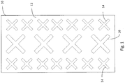
- FIG. 1 schematically diagrams a dual band antenna 10.
- the dual band antenna 10 includes a reflector 12, arrays of high band radiating elements 14, and an array oflow band radiating elements 16 interspersed with the high band elements.
- the high band radiating element 14 and low band element 16 may each comprise a cross dipole.
- Other radiating elements may be used, such as dipole squares, patch elements, single dipoles, etc.
- the present invention is not limited to dual band antennas, and may be used in any multiband application where higher band radiating elements and lower band radiating elements are present.
- the low band element 16 may optionally include a chokes on the dipole arms to reduce undesirable interference from the low band elements on the high band radiation pattern. See, e.g. PCT/CN2012/087300 .
- the dipole arms 15 of the high band element 14 may be supported over the reflector 12 by feed boards 18.
- the high band radiating elements 14 may be arranged in a sub-array.
- feed boards 18 are arranged on a backplane with a portion of a feed network to create a sub array.
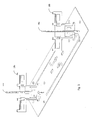
- FIG. 4a and 4b a first example of a feed board 18a for a high band radiating element 14 according to one aspect of the present invention is illustrated.
- the stalk traces capacitively couple signals from the feed network to the dipole arms of radiating elements 14.
- FIG. 4a and 4b two metallization layers of a feed board 18a are illustrated. These metallization layers are on opposite sides of a printed circuit board substrate.
- a first layer is illustrated in Figure 4a and a second layer is illustrated in Figure 4b .
- the first layers implements CM tuning circuits 20, hook balun 22, first capacitor sections 34, inductive elements 32, and second capacitor sections 30.
- the second layer implements stalks 24.
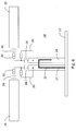
- FIG. 5a-5c Another example of a feed board including CM tuning circuits 20 is illustrated in Figures 5a-5c .
- FIG. 5a A first outer layer is illustrated in Figure 5a an inner layer is illustrated in Figure 5b , and a second outer layer is illustrated in Figure 5c .
- the middle layer implements the stalks 24.
- the first and second outer layers implement the CM tuning circuits 20, first capacitor sections 34, inductive elements 32, and second capacitor sections 30. Additionally, the first outer layer implements hook balun 22.
- FIG. 6 A schematic diagram of a high band radiating element 14 according to either of the examples of Figures 4a- 4b and Figures 5a-5c is illustrated in Figure 6 .
- Hook balun 22 couples with stalks 24 through the substrate of feed board 18 to transform a Radio Frequency (RF) signal in transmit direction from single-ended to balanced. (In the receive direction, the balun couples from balanced to unbalanced signals.)
- Stalks 24 propagate the balanced signals toward the dipole arms 15.
- First capacitor sections 34 capacitively couple to the stalks 24 through the substrate of feed board 18.
- Inductive traces 32 connect first capacitor sections 34 to second capacitor sections 30.
- Second capacitor sections 30 capacitively couple the RF signals to the dipole arms 15.
- the first capacitor section 34 is introduced to couple capacitively from the stalks 24 to the inductive sections 32 at high band frequencies where the dipole is desired to operate and acts to help block some of the low band currents from getting to the inductor sections 32.
- CM tuning circuits 20 provide a direct current (DC) path from first capacitor sections 34 to stalks 24 though a microstrip line and plated through-hole. Because stalks 24 are connected to ground at their lower-most edge, CM tuning circuits 20 provide a DC path to ground.
- the CM tuning circuits 20, in combination with capacitor sections 34, are preferably configured to act differently at low band and high band frequencies, and to suppress CM resonance at low band frequencies.
- the impedance of the CM tuning circuits 20 may be adjusted by varying a length and width of the metallic trace, and/or locating the CM tuning circuits over or to the side of a ground plane (e.g., stalk) on an opposite side of a layer of PCB substrate.
- CM tuning circuit 20 may comprise a narrow, high impedance microstrip line having length lw .
- the CM tuning circuit 20 may be dimensioned with a length to appear as a high impedance element at high band RF frequencies where it connects to capacitor section 34 near inductive section 32.
- the electrical length of 20 inversely proportional to frequency, and appears electrically shorter and lower in impedance at low band frequencies where it connects to capacitor section 34.
- the length lw may therefore be selected such that CM tuning circuit 20 does not adversely affect high band signals.
- CM resonance a plot of CM resonance versus frequency is illustrated.
- the high band radiating element is a dipole with a CLC feed circuit, but no CM tuning circuit 20.
- CM resonance is considerably reduced at low band frequencies, with a deep notch between 700MHz and 800MHz and a CM resonance below 700MHz.
- the CM tuning circuit 20 may be configured to move the CM resonance down below the low band frequency range.
- the CM resonance of the high band radiating element structure may be shifted by adjusting the length of the CM tuning circuit 20. In particular, the CM resonance may be shifted lower by increasing length lw .
- the low band radiating element in the absence of any high band radiating element, has a beamwidth of 58-65 degrees in at low band frequencies.
- the beamwidth undesirably widens to more than 74 degrees at about 840MHz, which is within the low band.
- the widening of the beamwidth is due to the CM resonance in the high band radiating element.
- This in-band CM resonance may also cause additional beam pattern distortions, such as large azimuth beam squint and poor Front/Back ratios.
- the beamwidth is much better above the CM resonance frequency (less than 60 degrees) than below the CM resonance frequency (more than 70 degrees), illustrating the benefit oftuning the CM resonance frequency to down below the low band.
- the CM resonance is indicated where the beamwidth widens to almost 80 degrees, which is at about 720MHz. This is well below 760MHz, which is outside the lower end of the low band frequency range.
- the beamwidth of the low band radiating elements is about 62 degrees, which is an improvement over techniques that tune the CM resonance frequency to be above the low band range, and the HB radiators of the present invention do not require expensive and bulky moats.
- the place where the CM tuning circuit 20 connects to the feed stalk may be varied to move CM resonance lower and out of band without detuning the high band radiating element.
- This solution is advantageous when a desired length lw of the CM tuning circuit 20 degrades or detunes the high band dipole.
- CM tuning circuit 20 depends solely on length lw , whereas the common mode responds is dependent on the total length of the signal path from second capacitor section 30 to stalk 24. Accordingly, the CM tuning circuit 20 attachment point may be adjusted closer to or further away from the second capacitor section 30 to adjust overall length of the CM tuing circuit 20 and to move the CM resonance back to the desired frequency.
Landscapes
- Variable-Direction Aerials And Aerial Arrays (AREA)
- Waveguide Aerials (AREA)
Priority Applications (2)
| Application Number | Priority Date | Filing Date | Title |
|---|---|---|---|
| EP21202123.2A EP3975338B1 (en) | 2015-01-15 | 2015-05-28 | Low common mode resonance multiband radiating array |
| PL20188138T PL3748772T3 (pl) | 2015-01-15 | 2015-05-28 | Rezonansowy, wielopasmowy szyk promieniujący o niskim trybie wspólnym |
Applications Claiming Priority (3)
| Application Number | Priority Date | Filing Date | Title |
|---|---|---|---|
| US201562103799P | 2015-01-15 | 2015-01-15 | |
| PCT/US2015/033013 WO2016114810A1 (en) | 2015-01-15 | 2015-05-28 | Low common mode resonance multiband radiating array |
| EP15727274.1A EP3245691B1 (en) | 2015-01-15 | 2015-05-28 | Low common mode resonance multiband radiating array |
Related Parent Applications (2)
| Application Number | Title | Priority Date | Filing Date |
|---|---|---|---|
| EP15727274.1A Division EP3245691B1 (en) | 2015-01-15 | 2015-05-28 | Low common mode resonance multiband radiating array |
| EP15727274.1A Division-Into EP3245691B1 (en) | 2015-01-15 | 2015-05-28 | Low common mode resonance multiband radiating array |
Related Child Applications (1)
| Application Number | Title | Priority Date | Filing Date |
|---|---|---|---|
| EP21202123.2A Division EP3975338B1 (en) | 2015-01-15 | 2015-05-28 | Low common mode resonance multiband radiating array |
Publications (2)
| Publication Number | Publication Date |
|---|---|
| EP3748772A1 EP3748772A1 (en) | 2020-12-09 |
| EP3748772B1 true EP3748772B1 (en) | 2021-10-13 |
Family
ID=53284675
Family Applications (3)
| Application Number | Title | Priority Date | Filing Date |
|---|---|---|---|
| EP20188138.0A Active EP3748772B1 (en) | 2015-01-15 | 2015-05-28 | Low common mode resonance multiband radiating array |
| EP21202123.2A Active EP3975338B1 (en) | 2015-01-15 | 2015-05-28 | Low common mode resonance multiband radiating array |
| EP15727274.1A Active EP3245691B1 (en) | 2015-01-15 | 2015-05-28 | Low common mode resonance multiband radiating array |
Family Applications After (2)
| Application Number | Title | Priority Date | Filing Date |
|---|---|---|---|
| EP21202123.2A Active EP3975338B1 (en) | 2015-01-15 | 2015-05-28 | Low common mode resonance multiband radiating array |
| EP15727274.1A Active EP3245691B1 (en) | 2015-01-15 | 2015-05-28 | Low common mode resonance multiband radiating array |
Country Status (8)
| Country | Link |
|---|---|
| US (1) | US9698486B2 (pl) |
| EP (3) | EP3748772B1 (pl) |
| DE (1) | DE202015009879U1 (pl) |
| DK (1) | DK3748772T3 (pl) |
| ES (1) | ES2902537T3 (pl) |
| FI (1) | FI3975338T3 (pl) |
| PL (1) | PL3748772T3 (pl) |
| WO (1) | WO2016114810A1 (pl) |
Families Citing this family (33)
| Publication number | Priority date | Publication date | Assignee | Title |
|---|---|---|---|---|
| WO2016081036A1 (en) | 2014-11-18 | 2016-05-26 | CommScope Technologies, LLC | Cloaked low band elements for multiband radiating arrays |
| CN106410396A (zh) * | 2016-10-26 | 2017-02-15 | 华南理工大学 | 一种高低频滤波阵子交织排列的紧凑型多波束天线阵列 |
| CN108155473B (zh) * | 2016-12-06 | 2024-05-14 | 普罗斯通信技术(苏州)有限公司 | 馈电结构及基站天线 |
| CN107359418B (zh) * | 2017-05-31 | 2019-11-29 | 上海华为技术有限公司 | 一种多频天线系统及控制多频天线系统内异频干扰的方法 |
| WO2018218515A1 (zh) * | 2017-05-31 | 2018-12-06 | 华为技术有限公司 | 天线馈电结构和天线辐射系统 |
| CN109149131B (zh) * | 2017-06-15 | 2021-12-24 | 康普技术有限责任公司 | 偶极天线和相关的多频带天线 |
| WO2019010051A1 (en) * | 2017-07-07 | 2019-01-10 | Commscope Technologies Llc | NARROWBAND RADIANT ELEMENTS WITH ULTRA-WIDE BAND WIDTH |
| EP3656017B1 (en) * | 2017-08-04 | 2025-10-08 | Huawei Technologies Co., Ltd. | Multiband antenna |
| WO2019032366A1 (en) * | 2017-08-07 | 2019-02-14 | Commscope Technologies Llc | CABLE CONNECTOR BLOCK ASSEMBLIES FOR BASE STATION ANTENNAS |
| EP3460906B1 (en) * | 2017-09-20 | 2023-05-03 | Alcatel-Lucent Shanghai Bell Co., Ltd. | Wireless telecommunication network antenna |
| KR102804667B1 (ko) * | 2018-05-15 | 2025-05-07 | 존 메짤링구아 어쏘시에이츠, 엘엘씨 | 고주파 대역에서 용이한 제작 및 제어 가능한 성능을 위한 패치 안테나 설계 |
| CN112335120B (zh) * | 2018-06-29 | 2023-09-19 | 上海诺基亚贝尔股份有限公司 | 多频带天线结构 |
| CN110931952B (zh) * | 2018-09-20 | 2021-12-24 | 上海华为技术有限公司 | 多频天线和通信设备 |
| CN111384594B (zh) * | 2018-12-29 | 2021-07-09 | 华为技术有限公司 | 高频辐射体、多频阵列天线和基站 |
| KR102125803B1 (ko) * | 2019-05-10 | 2020-06-23 | 주식회사 에이스테크놀로지 | 불요 공진 억제 기능을 가지는 기지국 안테나 방사체 |
| CN110444870B (zh) * | 2019-10-09 | 2020-01-03 | 华南理工大学 | 基站、宽带双极化滤波磁电偶极子天线及其辐射单元 |
| CN113328233B (zh) * | 2020-02-29 | 2022-11-08 | 华为技术有限公司 | 电子设备 |
| CN111478020A (zh) * | 2020-04-03 | 2020-07-31 | 深圳市大富科技股份有限公司 | 馈电网络以及天线馈电系统 |
| WO2021230922A1 (en) | 2020-05-15 | 2021-11-18 | John Mezzalingua Associates, Llc D/B/A Jma Wireless | Antenna radiator with pre-configured cloaking to enable dense placement of radiators of multiple bands |
| CN112134016B (zh) * | 2020-09-08 | 2025-02-28 | 京信通信技术(广州)有限公司 | 一种巴伦结构及其辐射单元、天线 |
| EP4211751A4 (en) | 2020-09-08 | 2024-10-02 | John Mezzalingua Associates, LLC | HIGH PERFORMANCE FOLDED DIPOLE FOR MULTIBAND ANTENNAS |
| CN112290199B (zh) * | 2020-09-29 | 2022-07-26 | 京信通信技术(广州)有限公司 | 天线及其低频辐射单元、隔离条 |
| GB2601810B (en) * | 2020-12-11 | 2023-07-05 | Alpha Wireless Ltd | High band antenna elements and a multi-band antenna |
| US11817629B2 (en) | 2020-12-21 | 2023-11-14 | John Mezzalingua Associates, LLC | Decoupled dipole configuration for enabling enhanced packing density for multiband antennas |
| CA3211410A1 (en) * | 2021-03-08 | 2022-09-15 | Jiaqiang ZHU | Broadband decoupled midband dipole for a dense multiband antenna |
| CN113270719B (zh) * | 2021-04-01 | 2023-04-11 | 中信科移动通信技术股份有限公司 | 天线隔离装置、阵列天线及基站天线 |
| US12555896B2 (en) * | 2021-12-31 | 2026-02-17 | Beijing Boe Sensor Technology Co., Ltd. | Transparent antenna and communication system |
| EP4483447A1 (en) | 2022-02-25 | 2025-01-01 | Telefonaktiebolaget LM Ericsson (publ) | Antenna and antenna array |
| CN116742317A (zh) * | 2022-03-01 | 2023-09-12 | 康普技术有限责任公司 | 具有包括基于超材料谐振器的偶极臂的宽带去耦辐射元件的基站天线 |
| WO2024132185A1 (en) | 2022-12-23 | 2024-06-27 | Telefonaktiebolaget Lm Ericsson (Publ) | Antenna, mobile communication base station and user device |
| WO2024165151A1 (en) | 2023-02-08 | 2024-08-15 | Telefonaktiebolaget Lm Ericsson (Publ) | Antenna, mobile communication base station and user device |
| WO2024228986A1 (en) * | 2023-05-01 | 2024-11-07 | John Mezzalingua Associates, LLC. | Aperture-fed patch c-band antenna array for ultra-dense multiband antennas |
| WO2026052207A1 (en) * | 2024-09-04 | 2026-03-12 | Telefonaktiebolaget Lm Ericsson (Publ) | A dipole antenna arrangement and array antenna |
Family Cites Families (8)
| Publication number | Priority date | Publication date | Assignee | Title |
|---|---|---|---|---|
| US7639196B2 (en) * | 2001-07-10 | 2009-12-29 | Andrew Llc | Cellular antenna and systems and methods therefor |
| US7173572B2 (en) * | 2002-02-28 | 2007-02-06 | Andrew Corporation | Dual band, dual pole, 90 degree azimuth BW, variable downtilt antenna |
| EP1509969A4 (en) * | 2002-03-26 | 2005-08-31 | Andrew Corp | MULTI-BAND ADJUSTABLE BASE STATION ANTENNA WITH INCLINE BEAM AND DUAL POLARIZATION |
| US20090122847A1 (en) * | 2007-09-04 | 2009-05-14 | Sierra Wireless, Inc. | Antenna Configurations for Compact Device Wireless Communication |
| US8350774B2 (en) | 2007-09-14 | 2013-01-08 | The United States Of America, As Represented By The Secretary Of The Navy | Double balun dipole |
| US8289218B2 (en) * | 2009-08-03 | 2012-10-16 | Venti Group, LLC | Cross-dipole antenna combination |
| US20110063190A1 (en) * | 2009-08-26 | 2011-03-17 | Jimmy Ho | Device and method for controlling azimuth beamwidth across a wide frequency range |
| US9276329B2 (en) * | 2012-11-22 | 2016-03-01 | Commscope Technologies Llc | Ultra-wideband dual-band cellular basestation antenna |
-
2015
- 2015-05-28 EP EP20188138.0A patent/EP3748772B1/en active Active
- 2015-05-28 PL PL20188138T patent/PL3748772T3/pl unknown
- 2015-05-28 ES ES20188138T patent/ES2902537T3/es active Active
- 2015-05-28 FI FIEP21202123.2T patent/FI3975338T3/fi active
- 2015-05-28 WO PCT/US2015/033013 patent/WO2016114810A1/en not_active Ceased
- 2015-05-28 DK DK20188138.0T patent/DK3748772T3/da active
- 2015-05-28 EP EP21202123.2A patent/EP3975338B1/en active Active
- 2015-05-28 EP EP15727274.1A patent/EP3245691B1/en active Active
- 2015-05-28 US US14/768,398 patent/US9698486B2/en active Active
- 2015-05-28 DE DE202015009879.7U patent/DE202015009879U1/de not_active Expired - Lifetime
Also Published As
| Publication number | Publication date |
|---|---|
| EP3748772A1 (en) | 2020-12-09 |
| US9698486B2 (en) | 2017-07-04 |
| PL3748772T3 (pl) | 2022-02-14 |
| FI3975338T3 (fi) | 2026-01-21 |
| DE202015009879U1 (de) | 2021-01-15 |
| EP3245691A1 (en) | 2017-11-22 |
| ES2902537T3 (es) | 2022-03-28 |
| US20160285169A1 (en) | 2016-09-29 |
| WO2016114810A1 (en) | 2016-07-21 |
| EP3975338B1 (en) | 2025-12-03 |
| DK3748772T3 (da) | 2022-01-03 |
| EP3245691B1 (en) | 2020-09-16 |
| EP3975338A1 (en) | 2022-03-30 |
Similar Documents
| Publication | Publication Date | Title |
|---|---|---|
| EP3748772B1 (en) | Low common mode resonance multiband radiating array | |
| US11688945B2 (en) | Method of eliminating resonances in multiband radiating arrays | |
| EP3221925B1 (en) | Cloaked low band elements for multiband radiating arrays | |
| US11196168B2 (en) | Ultra wide band radiators and related antennas arrays | |
| US11271327B2 (en) | Cloaking antenna elements and related multi-band antennas | |
| US10177438B2 (en) | Multi-band antenna arrays with common mode resonance (CMR) and differential mode resonance (DMR) removal | |
| US20190173186A1 (en) | Dipole antenna | |
| CN112768894A (zh) | 具有交叉偶极子辐射元件的多频带基站天线 | |
| WO2016137526A1 (en) | Full wave dipole array having improved squint performance | |
| US20250293441A1 (en) | Base station antennas having broadband decoupling radiating elements including metamaterial resonator based dipole arms | |
| KR100922230B1 (ko) | 다층 안테나 | |
| EP3618185B1 (en) | Radiating element for multi-band antenna and multi-band antenna | |
| KR100553269B1 (ko) | 다중대역 내장형 안테나 | |
| WO2025087548A1 (en) | Radiating element for a multiband antenna |
Legal Events
| Date | Code | Title | Description |
|---|---|---|---|
| PUAI | Public reference made under article 153(3) epc to a published international application that has entered the european phase |
Free format text: ORIGINAL CODE: 0009012 |
|
| STAA | Information on the status of an ep patent application or granted ep patent |
Free format text: STATUS: THE APPLICATION HAS BEEN PUBLISHED |
|
| AC | Divisional application: reference to earlier application |
Ref document number: 3245691 Country of ref document: EP Kind code of ref document: P |
|
| AK | Designated contracting states |
Kind code of ref document: A1 Designated state(s): AL AT BE BG CH CY CZ DE DK EE ES FI FR GB GR HR HU IE IS IT LI LT LU LV MC MK MT NL NO PL PT RO RS SE SI SK SM TR |
|
| STAA | Information on the status of an ep patent application or granted ep patent |
Free format text: STATUS: REQUEST FOR EXAMINATION WAS MADE |
|
| 17P | Request for examination filed |
Effective date: 20210217 |
|
| RBV | Designated contracting states (corrected) |
Designated state(s): AL AT BE BG CH CY CZ DE DK EE ES FI FR GB GR HR HU IE IS IT LI LT LU LV MC MK MT NL NO PL PT RO RS SE SI SK SM TR |
|
| GRAP | Despatch of communication of intention to grant a patent |
Free format text: ORIGINAL CODE: EPIDOSNIGR1 |
|
| STAA | Information on the status of an ep patent application or granted ep patent |
Free format text: STATUS: GRANT OF PATENT IS INTENDED |
|
| RIC1 | Information provided on ipc code assigned before grant |
Ipc: H01Q 1/52 20060101AFI20210414BHEP Ipc: H01Q 21/06 20060101ALI20210414BHEP Ipc: H01Q 1/24 20060101ALN20210414BHEP Ipc: H01Q 1/38 20060101ALN20210414BHEP Ipc: H01Q 21/26 20060101ALN20210414BHEP |
|
| INTG | Intention to grant announced |
Effective date: 20210429 |
|
| GRAS | Grant fee paid |
Free format text: ORIGINAL CODE: EPIDOSNIGR3 |
|
| GRAA | (expected) grant |
Free format text: ORIGINAL CODE: 0009210 |
|
| STAA | Information on the status of an ep patent application or granted ep patent |
Free format text: STATUS: THE PATENT HAS BEEN GRANTED |
|
| AC | Divisional application: reference to earlier application |
Ref document number: 3245691 Country of ref document: EP Kind code of ref document: P |
|
| AK | Designated contracting states |
Kind code of ref document: B1 Designated state(s): AL AT BE BG CH CY CZ DE DK EE ES FI FR GB GR HR HU IE IS IT LI LT LU LV MC MK MT NL NO PL PT RO RS SE SI SK SM TR |
|
| REG | Reference to a national code |
Ref country code: GB Ref legal event code: FG4D |
|
| REG | Reference to a national code |
Ref country code: CH Ref legal event code: EP |
|
| REG | Reference to a national code |
Ref country code: DE Ref legal event code: R096 Ref document number: 602015074206 Country of ref document: DE |
|
| REG | Reference to a national code |
Ref country code: IE Ref legal event code: FG4D |
|
| REG | Reference to a national code |
Ref country code: AT Ref legal event code: REF Ref document number: 1438852 Country of ref document: AT Kind code of ref document: T Effective date: 20211115 |
|
| REG | Reference to a national code |
Ref country code: FI Ref legal event code: FGE |
|
| REG | Reference to a national code |
Ref country code: DK Ref legal event code: T3 Effective date: 20211220 |
|
| REG | Reference to a national code |
Ref country code: SE Ref legal event code: TRGR |
|
| REG | Reference to a national code |
Ref country code: LT Ref legal event code: MG9D |
|
| REG | Reference to a national code |
Ref country code: NL Ref legal event code: MP Effective date: 20211013 |
|
| REG | Reference to a national code |
Ref country code: NO Ref legal event code: T2 Effective date: 20211013 |
|
| REG | Reference to a national code |
Ref country code: ES Ref legal event code: FG2A Ref document number: 2902537 Country of ref document: ES Kind code of ref document: T3 Effective date: 20220328 |
|
| PG25 | Lapsed in a contracting state [announced via postgrant information from national office to epo] |
Ref country code: RS Free format text: LAPSE BECAUSE OF FAILURE TO SUBMIT A TRANSLATION OF THE DESCRIPTION OR TO PAY THE FEE WITHIN THE PRESCRIBED TIME-LIMIT Effective date: 20211013 Ref country code: LT Free format text: LAPSE BECAUSE OF FAILURE TO SUBMIT A TRANSLATION OF THE DESCRIPTION OR TO PAY THE FEE WITHIN THE PRESCRIBED TIME-LIMIT Effective date: 20211013 Ref country code: BG Free format text: LAPSE BECAUSE OF FAILURE TO SUBMIT A TRANSLATION OF THE DESCRIPTION OR TO PAY THE FEE WITHIN THE PRESCRIBED TIME-LIMIT Effective date: 20220113 |
|
| PG25 | Lapsed in a contracting state [announced via postgrant information from national office to epo] |
Ref country code: IS Free format text: LAPSE BECAUSE OF FAILURE TO SUBMIT A TRANSLATION OF THE DESCRIPTION OR TO PAY THE FEE WITHIN THE PRESCRIBED TIME-LIMIT Effective date: 20220213 Ref country code: PT Free format text: LAPSE BECAUSE OF FAILURE TO SUBMIT A TRANSLATION OF THE DESCRIPTION OR TO PAY THE FEE WITHIN THE PRESCRIBED TIME-LIMIT Effective date: 20220214 Ref country code: NL Free format text: LAPSE BECAUSE OF FAILURE TO SUBMIT A TRANSLATION OF THE DESCRIPTION OR TO PAY THE FEE WITHIN THE PRESCRIBED TIME-LIMIT Effective date: 20211013 Ref country code: LV Free format text: LAPSE BECAUSE OF FAILURE TO SUBMIT A TRANSLATION OF THE DESCRIPTION OR TO PAY THE FEE WITHIN THE PRESCRIBED TIME-LIMIT Effective date: 20211013 Ref country code: HR Free format text: LAPSE BECAUSE OF FAILURE TO SUBMIT A TRANSLATION OF THE DESCRIPTION OR TO PAY THE FEE WITHIN THE PRESCRIBED TIME-LIMIT Effective date: 20211013 Ref country code: GR Free format text: LAPSE BECAUSE OF FAILURE TO SUBMIT A TRANSLATION OF THE DESCRIPTION OR TO PAY THE FEE WITHIN THE PRESCRIBED TIME-LIMIT Effective date: 20220114 |
|
| REG | Reference to a national code |
Ref country code: DE Ref legal event code: R097 Ref document number: 602015074206 Country of ref document: DE |
|
| PG25 | Lapsed in a contracting state [announced via postgrant information from national office to epo] |
Ref country code: SM Free format text: LAPSE BECAUSE OF FAILURE TO SUBMIT A TRANSLATION OF THE DESCRIPTION OR TO PAY THE FEE WITHIN THE PRESCRIBED TIME-LIMIT Effective date: 20211013 Ref country code: SK Free format text: LAPSE BECAUSE OF FAILURE TO SUBMIT A TRANSLATION OF THE DESCRIPTION OR TO PAY THE FEE WITHIN THE PRESCRIBED TIME-LIMIT Effective date: 20211013 Ref country code: RO Free format text: LAPSE BECAUSE OF FAILURE TO SUBMIT A TRANSLATION OF THE DESCRIPTION OR TO PAY THE FEE WITHIN THE PRESCRIBED TIME-LIMIT Effective date: 20211013 Ref country code: EE Free format text: LAPSE BECAUSE OF FAILURE TO SUBMIT A TRANSLATION OF THE DESCRIPTION OR TO PAY THE FEE WITHIN THE PRESCRIBED TIME-LIMIT Effective date: 20211013 Ref country code: CZ Free format text: LAPSE BECAUSE OF FAILURE TO SUBMIT A TRANSLATION OF THE DESCRIPTION OR TO PAY THE FEE WITHIN THE PRESCRIBED TIME-LIMIT Effective date: 20211013 |
|
| PLBE | No opposition filed within time limit |
Free format text: ORIGINAL CODE: 0009261 |
|
| STAA | Information on the status of an ep patent application or granted ep patent |
Free format text: STATUS: NO OPPOSITION FILED WITHIN TIME LIMIT |
|
| 26N | No opposition filed |
Effective date: 20220714 |
|
| PG25 | Lapsed in a contracting state [announced via postgrant information from national office to epo] |
Ref country code: AL Free format text: LAPSE BECAUSE OF FAILURE TO SUBMIT A TRANSLATION OF THE DESCRIPTION OR TO PAY THE FEE WITHIN THE PRESCRIBED TIME-LIMIT Effective date: 20211013 |
|
| PG25 | Lapsed in a contracting state [announced via postgrant information from national office to epo] |
Ref country code: SI Free format text: LAPSE BECAUSE OF FAILURE TO SUBMIT A TRANSLATION OF THE DESCRIPTION OR TO PAY THE FEE WITHIN THE PRESCRIBED TIME-LIMIT Effective date: 20211013 |
|
| REG | Reference to a national code |
Ref country code: CH Ref legal event code: PL |
|
| REG | Reference to a national code |
Ref country code: AT Ref legal event code: UEP Ref document number: 1438852 Country of ref document: AT Kind code of ref document: T Effective date: 20211013 |
|
| PG25 | Lapsed in a contracting state [announced via postgrant information from national office to epo] |
Ref country code: MC Free format text: LAPSE BECAUSE OF FAILURE TO SUBMIT A TRANSLATION OF THE DESCRIPTION OR TO PAY THE FEE WITHIN THE PRESCRIBED TIME-LIMIT Effective date: 20211013 Ref country code: LU Free format text: LAPSE BECAUSE OF NON-PAYMENT OF DUE FEES Effective date: 20220528 Ref country code: LI Free format text: LAPSE BECAUSE OF NON-PAYMENT OF DUE FEES Effective date: 20220531 Ref country code: CH Free format text: LAPSE BECAUSE OF NON-PAYMENT OF DUE FEES Effective date: 20220531 |
|
| P01 | Opt-out of the competence of the unified patent court (upc) registered |
Effective date: 20230530 |
|
| PG25 | Lapsed in a contracting state [announced via postgrant information from national office to epo] |
Ref country code: MK Free format text: LAPSE BECAUSE OF FAILURE TO SUBMIT A TRANSLATION OF THE DESCRIPTION OR TO PAY THE FEE WITHIN THE PRESCRIBED TIME-LIMIT Effective date: 20211013 Ref country code: CY Free format text: LAPSE BECAUSE OF FAILURE TO SUBMIT A TRANSLATION OF THE DESCRIPTION OR TO PAY THE FEE WITHIN THE PRESCRIBED TIME-LIMIT Effective date: 20211013 |
|
| PG25 | Lapsed in a contracting state [announced via postgrant information from national office to epo] |
Ref country code: HU Free format text: LAPSE BECAUSE OF FAILURE TO SUBMIT A TRANSLATION OF THE DESCRIPTION OR TO PAY THE FEE WITHIN THE PRESCRIBED TIME-LIMIT; INVALID AB INITIO Effective date: 20150528 |
|
| REG | Reference to a national code |
Ref country code: FI Ref legal event code: PCE Owner name: OUTDOOR WIRELESS NETWORKS LLC |
|
| REG | Reference to a national code |
Ref country code: GB Ref legal event code: 732E Free format text: REGISTERED BETWEEN 20240815 AND 20240821 |
|
| REG | Reference to a national code |
Ref country code: DE Ref legal event code: R081 Ref document number: 602015074206 Country of ref document: DE Owner name: OUTDOOR WIRELESS NETWORKS LLC (A COMPANY ORGAN, US Free format text: FORMER OWNER: COMMSCOPE TECHNOLOGIES LLC, HICKORY, NC, US |
|
| PG25 | Lapsed in a contracting state [announced via postgrant information from national office to epo] |
Ref country code: MT Free format text: LAPSE BECAUSE OF FAILURE TO SUBMIT A TRANSLATION OF THE DESCRIPTION OR TO PAY THE FEE WITHIN THE PRESCRIBED TIME-LIMIT Effective date: 20211013 |
|
| REG | Reference to a national code |
Ref country code: ES Ref legal event code: PC2A Owner name: OUTDOOR WIRELESS NETWORKS LLC. Effective date: 20241111 |
|
| REG | Reference to a national code |
Ref country code: AT Ref legal event code: PC Ref document number: 1438852 Country of ref document: AT Kind code of ref document: T Owner name: OUTDOOR WIRELESS NETWORKS LLC, US Effective date: 20241021 |
|
| REG | Reference to a national code |
Ref country code: BE Ref legal event code: PD Owner name: OUTDOOR WIRELESS NETWORKS LLC; US Free format text: DETAILS ASSIGNMENT: CHANGE OF OWNER(S), ASSIGNMENT; FORMER OWNER NAME: COMMSCOPE TECHNOLOGIES LLC Effective date: 20241209 |
|
| PGFP | Annual fee paid to national office [announced via postgrant information from national office to epo] |
Ref country code: FI Payment date: 20250526 Year of fee payment: 11 |
|
| PGFP | Annual fee paid to national office [announced via postgrant information from national office to epo] |
Ref country code: DE Payment date: 20250529 Year of fee payment: 11 Ref country code: PL Payment date: 20250508 Year of fee payment: 11 |
|
| PGFP | Annual fee paid to national office [announced via postgrant information from national office to epo] |
Ref country code: GB Payment date: 20250527 Year of fee payment: 11 Ref country code: ES Payment date: 20250602 Year of fee payment: 11 Ref country code: DK Payment date: 20250526 Year of fee payment: 11 |
|
| PGFP | Annual fee paid to national office [announced via postgrant information from national office to epo] |
Ref country code: NO Payment date: 20250530 Year of fee payment: 11 |
|
| PGFP | Annual fee paid to national office [announced via postgrant information from national office to epo] |
Ref country code: BE Payment date: 20250527 Year of fee payment: 11 Ref country code: IT Payment date: 20250521 Year of fee payment: 11 |
|
| PGFP | Annual fee paid to national office [announced via postgrant information from national office to epo] |
Ref country code: FR Payment date: 20250526 Year of fee payment: 11 |
|
| PGFP | Annual fee paid to national office [announced via postgrant information from national office to epo] |
Ref country code: AT Payment date: 20250505 Year of fee payment: 11 |
|
| PGFP | Annual fee paid to national office [announced via postgrant information from national office to epo] |
Ref country code: IE Payment date: 20250527 Year of fee payment: 11 |
|
| PGFP | Annual fee paid to national office [announced via postgrant information from national office to epo] |
Ref country code: SE Payment date: 20250527 Year of fee payment: 11 |
|
| PG25 | Lapsed in a contracting state [announced via postgrant information from national office to epo] |
Ref country code: TR Free format text: LAPSE BECAUSE OF FAILURE TO SUBMIT A TRANSLATION OF THE DESCRIPTION OR TO PAY THE FEE WITHIN THE PRESCRIBED TIME-LIMIT Effective date: 20211013 |