EP3748668A1 - Reactive ion etching device - Google Patents
Reactive ion etching device Download PDFInfo
- Publication number
- EP3748668A1 EP3748668A1 EP18902867.3A EP18902867A EP3748668A1 EP 3748668 A1 EP3748668 A1 EP 3748668A1 EP 18902867 A EP18902867 A EP 18902867A EP 3748668 A1 EP3748668 A1 EP 3748668A1
- Authority
- EP
- European Patent Office
- Prior art keywords
- capacitor
- processed substrate
- radio
- etching
- electrodes
- Prior art date
- Legal status (The legal status is an assumption and is not a legal conclusion. Google has not performed a legal analysis and makes no representation as to the accuracy of the status listed.)
- Granted
Links
Images
Classifications
-
- H—ELECTRICITY
- H10—SEMICONDUCTOR DEVICES; ELECTRIC SOLID-STATE DEVICES NOT OTHERWISE PROVIDED FOR
- H10P—GENERIC PROCESSES OR APPARATUS FOR THE MANUFACTURE OR TREATMENT OF DEVICES COVERED BY CLASS H10
- H10P72/00—Handling or holding of wafers, substrates or devices during manufacture or treatment thereof
- H10P72/04—Apparatus for manufacture or treatment
- H10P72/0402—Apparatus for fluid treatment
- H10P72/0418—Apparatus for fluid treatment for etching
- H10P72/0421—Apparatus for fluid treatment for etching for drying etching
-
- H—ELECTRICITY
- H10—SEMICONDUCTOR DEVICES; ELECTRIC SOLID-STATE DEVICES NOT OTHERWISE PROVIDED FOR
- H10P—GENERIC PROCESSES OR APPARATUS FOR THE MANUFACTURE OR TREATMENT OF DEVICES COVERED BY CLASS H10
- H10P50/00—Etching of wafers, substrates or parts of devices
- H10P50/20—Dry etching; Plasma etching; Reactive-ion etching
- H10P50/24—Dry etching; Plasma etching; Reactive-ion etching of semiconductor materials
- H10P50/242—Dry etching; Plasma etching; Reactive-ion etching of semiconductor materials of Group IV materials
-
- H—ELECTRICITY
- H01—ELECTRIC ELEMENTS
- H01J—ELECTRIC DISCHARGE TUBES OR DISCHARGE LAMPS
- H01J37/00—Discharge tubes with provision for introducing objects or material to be exposed to the discharge, e.g. for the purpose of examination or processing thereof
- H01J37/32—Gas-filled discharge tubes
- H01J37/32009—Arrangements for generation of plasma specially adapted for examination or treatment of objects, e.g. plasma sources
- H01J37/32082—Radio frequency generated discharge
- H01J37/32091—Radio frequency generated discharge the radio frequency energy being capacitively coupled to the plasma
-
- H—ELECTRICITY
- H01—ELECTRIC ELEMENTS
- H01J—ELECTRIC DISCHARGE TUBES OR DISCHARGE LAMPS
- H01J37/00—Discharge tubes with provision for introducing objects or material to be exposed to the discharge, e.g. for the purpose of examination or processing thereof
- H01J37/32—Gas-filled discharge tubes
- H01J37/32009—Arrangements for generation of plasma specially adapted for examination or treatment of objects, e.g. plasma sources
- H01J37/32082—Radio frequency generated discharge
- H01J37/32137—Radio frequency generated discharge controlling of the discharge by modulation of energy
- H01J37/32155—Frequency modulation
- H01J37/32165—Plural frequencies
-
- H—ELECTRICITY
- H01—ELECTRIC ELEMENTS
- H01J—ELECTRIC DISCHARGE TUBES OR DISCHARGE LAMPS
- H01J37/00—Discharge tubes with provision for introducing objects or material to be exposed to the discharge, e.g. for the purpose of examination or processing thereof
- H01J37/32—Gas-filled discharge tubes
- H01J37/32009—Arrangements for generation of plasma specially adapted for examination or treatment of objects, e.g. plasma sources
- H01J37/32082—Radio frequency generated discharge
- H01J37/32174—Circuits specially adapted for controlling the RF discharge
-
- H—ELECTRICITY
- H01—ELECTRIC ELEMENTS
- H01J—ELECTRIC DISCHARGE TUBES OR DISCHARGE LAMPS
- H01J37/00—Discharge tubes with provision for introducing objects or material to be exposed to the discharge, e.g. for the purpose of examination or processing thereof
- H01J37/32—Gas-filled discharge tubes
- H01J37/32431—Constructional details of the reactor
- H01J37/32532—Electrodes
- H01J37/32568—Relative arrangement or disposition of electrodes; moving means
-
- H—ELECTRICITY
- H01—ELECTRIC ELEMENTS
- H01J—ELECTRIC DISCHARGE TUBES OR DISCHARGE LAMPS
- H01J37/00—Discharge tubes with provision for introducing objects or material to be exposed to the discharge, e.g. for the purpose of examination or processing thereof
- H01J37/32—Gas-filled discharge tubes
- H01J37/32431—Constructional details of the reactor
- H01J37/32532—Electrodes
- H01J37/32577—Electrical connecting means
-
- H—ELECTRICITY
- H01—ELECTRIC ELEMENTS
- H01J—ELECTRIC DISCHARGE TUBES OR DISCHARGE LAMPS
- H01J37/00—Discharge tubes with provision for introducing objects or material to be exposed to the discharge, e.g. for the purpose of examination or processing thereof
- H01J37/32—Gas-filled discharge tubes
- H01J37/32431—Constructional details of the reactor
- H01J37/32697—Electrostatic control
-
- H—ELECTRICITY
- H01—ELECTRIC ELEMENTS
- H01J—ELECTRIC DISCHARGE TUBES OR DISCHARGE LAMPS
- H01J37/00—Discharge tubes with provision for introducing objects or material to be exposed to the discharge, e.g. for the purpose of examination or processing thereof
- H01J37/32—Gas-filled discharge tubes
- H01J37/32431—Constructional details of the reactor
- H01J37/32697—Electrostatic control
- H01J37/32706—Polarising the substrate
-
- H—ELECTRICITY
- H02—GENERATION; CONVERSION OR DISTRIBUTION OF ELECTRIC POWER
- H02N—ELECTRIC MACHINES NOT OTHERWISE PROVIDED FOR
- H02N13/00—Clutches or holding devices using electrostatic attraction, e.g. using Johnson-Rahbek effect
-
- H—ELECTRICITY
- H05—ELECTRIC TECHNIQUES NOT OTHERWISE PROVIDED FOR
- H05H—PLASMA TECHNIQUE; PRODUCTION OF ACCELERATED ELECTRICALLY-CHARGED PARTICLES OR OF NEUTRONS; PRODUCTION OR ACCELERATION OF NEUTRAL MOLECULAR OR ATOMIC BEAMS
- H05H1/00—Generating plasma; Handling plasma
- H05H1/24—Generating plasma
- H05H1/46—Generating plasma using applied electromagnetic fields, e.g. high frequency or microwave energy
-
- H—ELECTRICITY
- H10—SEMICONDUCTOR DEVICES; ELECTRIC SOLID-STATE DEVICES NOT OTHERWISE PROVIDED FOR
- H10P—GENERIC PROCESSES OR APPARATUS FOR THE MANUFACTURE OR TREATMENT OF DEVICES COVERED BY CLASS H10
- H10P72/00—Handling or holding of wafers, substrates or devices during manufacture or treatment thereof
- H10P72/70—Handling or holding of wafers, substrates or devices during manufacture or treatment thereof for supporting or gripping
- H10P72/72—Handling or holding of wafers, substrates or devices during manufacture or treatment thereof for supporting or gripping using electrostatic chucks
- H10P72/722—Details of electrostatic chucks
Definitions
- the present invention relates to a reactive ion etching apparatus.
- a reactive ion etching apparatus which utilizes vacuum atmosphere in order to selectively remove metallic films and insulating films that are formed on the surface of a substrate such as a silicon wafer and the like.
- This reactive ion etching apparatus generally comprises: a stage on which a substrate to be processed (hereinafter referred to as a "to-be-processed substrate”) is disposed inside a vacuum chamber; a gas introduction means for introducing an etching gas into the vacuum chamber in vacuum atmosphere; a plasma generation means for generating inside the vacuum chamber a plasma which ionizes the introduced etching gas; and a radio-frequency power source which is connected to the stage through an output line so as to apply bias potential to the to-be-processed substrate.
- a stage on which a substrate to be processed hereinafter referred to as a "to-be-processed substrate”
- a gas introduction means for introducing an etching gas into the vacuum chamber in vacuum atmosphere
- a plasma generation means for generating inside the vacuum chamber a plasma which ionizes the introduced etching gas
- a radio-frequency power source which is connected to the stage through an output line so as to apply bias potential to the to-be-processed substrate
- Patent Document 1 in which is disclosed that two sets of radio-frequency power sources are used to thereby respectively supply a first electrode (inside electrode) and a second electrode (outside electrode) with radio-frequency power of different frequencies, the first and the second electrodes being disposed on a stage in a state of being electrically insulated from each other.
- the distribution of the bias potential to be applied to the to-be-processed substrate is changed, thereby obtaining a substantially uniform etching rate over the entire to-be-processed substrate.
- the above-mentioned conventional example employs two radio-frequency power sources (and distributors), there is a problem in that the costs for the apparatus become expensive and also that the arrangement of the apparatus becomes complicated.
- the to-be-processed substrate is subjected to etching processing by using the above-mentioned reactive ion etching apparatus, it sometimes happens that the to-be-processed substrate is controlled at a predetermined temperature.
- Patent Document 1 JP-2011-228436-A
- this invention has a problem of providing a reactive ion etching apparatus which is low in cost and simple in construction and also which is capable of obtaining a substantially uniform etching rate over the entire in-plane direction of the to-be-processed substrate.
- a reactive ion etching apparatus comprises: a stage on which a to-be-processed substrate is disposed inside a vacuum chamber; a gas introduction means for introducing an etching gas into the vacuum chamber in vacuum atmosphere; a plasma generation means for generating inside the vacuum chamber a plasma which ionizes the introduced etching gas; a radio-frequency power source connected to the stage through a first output line so as to apply bias potential to the to-be-processed substrate; the stage being provided with an electrostatic chuck having a pair of electrodes so that, at the time of etching the to-be-processed substrate, DC voltage is applied to the pair of electrodes, whereby the to-be-processed substrate is electrostatically absorbed to the electrostatic chuck.
- the radio-frequency power source is arranged to be connected, through a second output line, to the pair of electrodes so as to apply radio-frequency potential in a manner to be superposed on the DC voltage; both a first capacitor and a second capacitor are interposed respectively in the first output line and the second output line; and a capacitance ratio of the first capacitor to the second capacitor is set to a range of 0.25 to 25.
- the radio-frequency potential is applied in a manner to be superposed on the DC power that is applied in electrostatically absorbing the to-be-processed substrate.
- the capacitance ratio of the first capacitor to the second capacitor is set to a range of 0.25 to 25. Therefore, the distribution of the bias potential that is applied to the to-be-processed substrate is adjusted so that a substantially uniform etching rate comes to be obtainable over the entire surface of the to-be-processed substrate.
- bias potential is applied by a single radio-frequency power source by making use of the pair of electrodes of the electrostatic chuck.
- At least one of the first capacitor and the second capacitor shall preferably be a variable capacitor whose capacitance is variable.
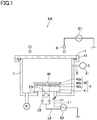
- FIG. 1 is a sectional view to schematically explain the constitution of an embodiment of the etching apparatus of this invention.
- etching apparauts an embodiment of a reactive etching apparatus of this invention
- FIG. 1 the terms referring to the directions shall be based on FIG. 1 .
- reference mark EM denotes an etching apparatus.
- the etching apparatus EM is provided with a vacuum chamber 1 which is capable of forming a vacuum atmosphere by evacuation with a vacuum pump P.
- An upper opening of the vacuum chamber 1 has mounted thereon, through a vacuum seal 11 such as an O-ring and the like, a ceiling plate 12 made of a dielectric material such as quartz and the like.
- the side wall of the vacuum chamber 1 has connected thereto a gas pipe 2 which is in communication with a gas source (not illustrated).
- the gas pipe 2 has interposed therein a mass flow controller 21. It is thus so arranged that an etching gas can be introduced into the vacuum chamber 1 in a predetermined amount.
- the etching gas is appropriately selected depending on the object to be subjected to etching.
- etching gas for example, in case metallic films such as of aluminum, tungsten, and the like, are to be subjected to etching, chlorine gases such as Cl 2 , BCl 3 , CCl 4 and the like are mainly used and, depending on the necessity, inert gas and the like as diluent gas is added.
- the gas pipe 2 and the mass flow controller 21 constitute the "gas introduction means" of this invention.
- the ceiling plate 12 there are provided a plurality of stages (two stages in this embodiment) of loop antenna coils 3. Output from the radio-frequency power source E1 is connected to these antenna coils 3 so that the radio-frequency power for plasma generation can be supplied. These antenna coils 3 and the radio-frequency power source E1 can constitute "plasma generation means" of this invention. At the bottom portion inside the vacuum chamber 1 there is disposed a stage 4.
- the stage 4 is provided with: a base 41 which is disposed, through an insulating body I, at the bottom of the vacuum chamber 1, and which is constituted by a tubular body made of a metallic cylindrical material; and an electrostatic chuck 42 which is disposed on an upper surface of the base 41.
- the base 41 has built therein: a heating means having a heater, and the like; and a cooling means having coolant circulation passages. It is thus so arranged that, at the time of etching, the to-be-processed substrate W can be heated or cooled to a predetermined temperature.
- the base 41 has further connected thereto, through a first output line L1, a radio-frequency power source E2. It is thus so arranged that, at the time of etching, by supplying the radio-frequency power of a predetermined frequency from the radio-frequency power source E2, bias potential can be applied to the to-be-processed substrate W.
- the electrostatic chuck 42 has: a chuck plate 42a which is closely adhered to the upper surface of the base 41 and which is made of a dielectric; and a pair of electrdes 42b, 42c which are buried in the chuck plate 42a. To both the electrodes 42b, 42c there is respectively connected an output cable from a DC power source E3. It is thus so arranged that, by applying predetermined DC voltage across the pair of electrodes 42b, 42c, the to-be-processed substrate W can be electrostatically absorbed to the upper surface of the chuck plate 42a.
- both the electrodes 42b, 42c are respectively constituted by, e.g., metal plates formed into the shape of a comb, and are disposed such that the tooth portions thereof, in a posture of being in mesh with each other, are present substantially over the entire area of the same plane of the chuck plate 42a.
- the shape, the manner of disposing, and the like of each of the electrodes 42b, 42c shall not be limited to the above.
- the radio-frequency power source E2 is connected also to the pair of electrodes 42b, 42c through the second output line L2; and that radio-frequency potential can be applied to the pair of electrodes 42b, 42c in a manner to be superposed on the above-mentioned DC voltage.
- the first and the second output lines L1, L2 have interposed therein a first capacitor C1 and a second capacitor C2, respectively.
- a variable capacitor is used as the first capacitor C1 and a fixed capacitor is used as the second capacitor C2.
- the variable capacitor C1 there may be cited an example whose capacitance is variable, e.g., between 12.5 and 5000 pF and, as the fixed capacitor C2, there may be cited an example having a predetermined capacitance, e.g., between 50 and 200 pF.
- selection may appropriately be made out of an electrolytic capacitor, ceramic capacitor, film capacitor, electric double-layer capactor, and the like.
- the capacitance of the first capacitor C1 is appropriately changed so that the capacitance ratio of the first capacitor C1 to the second capacitor C2 is set to a range of 0.25 to 25.
- the capacitance ratio lies outside the range of 0.25 to 25, there is a possibility of giving rise to a problem in that in-plane uniformity at the desired etching rate cannot be obtained.
- the above-mentioned etching apparatus EM has, although not illustrated, a known control means provided with a microcomputer, sequencer, and the like.
- the control means performes an overall control of: the operation of the above-mentioned respective power sources E1, E2, E3; the operation of the massflow controller 21; the operation of the vacuum pump; and the like.
- the control means also adjusts the capacitance ratio of the variable capacitor C1 to the fixed capacitor C2 by adjusting the capacitance of the variable capacitor C1.
- the to-be-processed substrate W is transferred, by using a transfer robot (not illustrated), onto a chuck plate 42a of the stage 4. Then, DC voltage is applied from the DC power source E3 to the pair of electrodes 42b, 42c of the electrostatic chuck 42. The to-be-processed substrate W is thereby electrostatically absorbed to the upper surface of the chuck plate 42a.
- a desired vacuum degree e.g., 0.5 Pa
- chroline gas is introduced into the vacuum chamber 1 at a flow rate of 20 to 200 sccm and, at the same time, by supplying radio-frequency power of, e.g., 13.56 MHz from the radio-frequency power source E1 to the antenna coil 3 at 100 W to 1000 W, a plasma is caused to be generated inside the vacuum chamber 1.
- radio-frequency power e.g., 13.56 MHz from the radio-frequency power source E1 to the antenna coil 3 at 100 W to 1000 W
- bias potential is applied to the to-be-processed substrate W. According to these operations, the ions that have been dissociated in the plasma are attracted to the surface of the to-be-processed substrate W, thereby performing dry etching of the aluminum film.
- radio-frequency potential is applied from the radio-frequency power source E2 to the pair of electrodes 42b, 42c in a manner to be superposed on the DC voltage.
- the capacitance ratio of the first capacitor C1 to the second capacitor C2 is set to a range of 0.25 to 25.
- the in-plane uniformity of the etching rate of the aluminum film was able to be increased below ⁇ 3.5 %, more preferably below ⁇ 2.0 %.
- the bias potential is applied by a single radio-freuquency power source E2 by making use of the pair of electrodes 42b, 42c of the electrostatic chuck 42. Therefore, as compared with the above-mentioned conventional example in which two bias radio-frequency power sources (and distributors) are used, the apparatus arrangement of this embodiment can be made simpler and the apparatus cost can be reduced.
- the object to be subjected to etching such as metallic films, insulating films, and the like
- etching conditions kind of etching gas, pressure at the time of etching
- the bias potential being the one at which a substantially uniform etching rate can be obtained over the entire surface of the to-be-processed substrate W.
- the distribution of the bias potential can advantageously be adjusted depending on the object to be subjected to etching, or the etching conditions.
- the substrate W is defined to be the one in which an aluminum film was formed, by a sputtering method, to a thickness of about 300 nm on a silicon substrate W.
- This aluminum film was subjected to etching on the following conditions.
- the flow rate of the chlorine gas (e.g., Cl 2 , BCl 3 ) was set at 50 sccm, 50 sccm (the pressure inside the vacuum chamber 1 at this time was 0.5 Pa); the bias power to be supplied to the stage 4 was set to 12.5 MHz, 150 W; power to be supplied to the antenna coil 3 was set to 13.56 MHz, 300 W; and DC volatage to be applied to the electrostatic chuck 42 was set to 1.0 kV.
- the first capacitor C1 a variable capacitor whose capacitance is variable was used as the first capacitor C1 a variable capacitor whose capacitance is variable was used.
- the second capacitor C2 a fixed capacitor whose capacitance is fixed (200 pF) was used, and the capacitance of the variable capacitor C1 was adjusted to 2500 pF (the capacitance ratio of the first capacitor C1 to the second capacitor C2 at this time was 12.5, hereinafter referred to as "Invention Experiment 1").
- the film thicknesses of the aluminum film before and after etching in the Invention Experiment 1 were measured at 7 points, respectively, in the radial direction of the to-be-processed substrate W.
- An average value of the etching rate as obtained from the above-mentioned measured values was 350 nm/min., and the in-plane uniformity was ⁇ 1.8 %.
- etching was performed in a manner similar to that in the above-mentioned Invention Experiment 1, and then average values of the etching rate and the in-plane uniformity were obtained.
- the description was made of an example in which the first capacitor C1 was made to be a variable capacitor and in which the second capacitor C2 was made to be a fixed capacitor.
- the first capacitor C1 and the second capacitor C2 shall be a variable capacitor.
- the first capacitor C1 may be made to be a fixed capacitor and the second capacitor C2 may be made to be a variable capacitor.
- the distribution of the bias potential can appropriately be adjusted depending on the object to be subjected to etching as well as on the etching conditions.
Landscapes
- Physics & Mathematics (AREA)
- Engineering & Computer Science (AREA)
- Plasma & Fusion (AREA)
- Chemical & Material Sciences (AREA)
- Analytical Chemistry (AREA)
- Electromagnetism (AREA)
- Spectroscopy & Molecular Physics (AREA)
- Drying Of Semiconductors (AREA)
- Plasma Technology (AREA)
- Container, Conveyance, Adherence, Positioning, Of Wafer (AREA)
- Crystals, And After-Treatments Of Crystals (AREA)
Abstract
Description
- The present invention relates to a reactive ion etching apparatus.
- In the steps of manufacturing, e.g., a semiconductor device, there has conventionally been used a reactive ion etching apparatus which utilizes vacuum atmosphere in order to selectively remove metallic films and insulating films that are formed on the surface of a substrate such as a silicon wafer and the like. This reactive ion etching apparatus generally comprises: a stage on which a substrate to be processed (hereinafter referred to as a "to-be-processed substrate") is disposed inside a vacuum chamber; a gas introduction means for introducing an etching gas into the vacuum chamber in vacuum atmosphere; a plasma generation means for generating inside the vacuum chamber a plasma which ionizes the introduced etching gas; and a radio-frequency power source which is connected to the stage through an output line so as to apply bias potential to the to-be-processed substrate.
- Now, to-be-processed substrates have recently become larger in area, and it is required that a substantially uniform etching rate be obtainable over the entire in-plane direction of the to-be-processed substrates even with this kind of to-be-processed substrates. There is known conventional art in, e.g.,
Patent Document 1, in which is disclosed that two sets of radio-frequency power sources are used to thereby respectively supply a first electrode (inside electrode) and a second electrode (outside electrode) with radio-frequency power of different frequencies, the first and the second electrodes being disposed on a stage in a state of being electrically insulated from each other. In this arrangement, by varying the power ratio to be applied to the first electrode and the second electrode, the distribution of the bias potential to be applied to the to-be-processed substrate is changed, thereby obtaining a substantially uniform etching rate over the entire to-be-processed substrate. - However, since the above-mentioned conventional example employs two radio-frequency power sources (and distributors), there is a problem in that the costs for the apparatus become expensive and also that the arrangement of the apparatus becomes complicated. By the way, in case the to-be-processed substrate is subjected to etching processing by using the above-mentioned reactive ion etching apparatus, it sometimes happens that the to-be-processed substrate is controlled at a predetermined temperature. In such a case, it is normal practice to build into the stage a heating means and a cooling means, and also to provide the stage with a so-called electrostatic chuck. Since the electrostatic chuck is ordinarily provided with a pair of electrodes for electrostatically absorbing the to-be-processed substrate, they can be used to advantage in order to reduce the apparatus cost and to simplify the apparatus arrangement.
- Patent Document 1:
JP-2011-228436-A - In view of the above-mentioned points, this invention has a problem of providing a reactive ion etching apparatus which is low in cost and simple in construction and also which is capable of obtaining a substantially uniform etching rate over the entire in-plane direction of the to-be-processed substrate.
- In order to solve the above-mentioned problems, a reactive ion etching apparatus comprises: a stage on which a to-be-processed substrate is disposed inside a vacuum chamber; a gas introduction means for introducing an etching gas into the vacuum chamber in vacuum atmosphere; a plasma generation means for generating inside the vacuum chamber a plasma which ionizes the introduced etching gas; a radio-frequency power source connected to the stage through a first output line so as to apply bias potential to the to-be-processed substrate; the stage being provided with an electrostatic chuck having a pair of electrodes so that, at the time of etching the to-be-processed substrate, DC voltage is applied to the pair of electrodes, whereby the to-be-processed substrate is electrostatically absorbed to the electrostatic chuck. In the reactive ion etching apparatus: the radio-frequency power source is arranged to be connected, through a second output line, to the pair of electrodes so as to apply radio-frequency potential in a manner to be superposed on the DC voltage; both a first capacitor and a second capacitor are interposed respectively in the first output line and the second output line; and a capacitance ratio of the first capacitor to the second capacitor is set to a range of 0.25 to 25.
- According to this invention, at the time of etching the to-be-processed substrate, by making use of the pair of electrodes of the electrostatic chuck, the radio-frequency potential is applied in a manner to be superposed on the DC power that is applied in electrostatically absorbing the to-be-processed substrate. At this time, the capacitance ratio of the first capacitor to the second capacitor is set to a range of 0.25 to 25. Therefore, the distribution of the bias potential that is applied to the to-be-processed substrate is adjusted so that a substantially uniform etching rate comes to be obtainable over the entire surface of the to-be-processed substrate. In this manner, according to this invention, while maintaining the function in that a substantially uniform etching rate can be obtained over the entire surface of the to-be-processed substrate, bias potential is applied by a single radio-frequency power source by making use of the pair of electrodes of the electrostatic chuck. Therefor, as compared with the above-mentioned conventional case in which two radio-frequency power sources are used, the arrangement of the apparatus can be simplified and the apparatus costs can be reduced.
- In this invention, in order to enable to appropriately adjust the distribution of the bias potential depending on the to-be-processed object (metallic film and insulating film), at least one of the first capacitor and the second capacitor shall preferably be a variable capacitor whose capacitance is variable.
- [
FIG. 1 ] is a sectional view to schematically explain the constitution of an embodiment of the etching apparatus of this invention. - Hereinbelow, with reference to the drawing, a description will now be made of an embodiment of a reactive etching apparatus of this invention (hereinafter referred to as an "etching apparauts"). In the following description, the terms referring to the directions shall be based on
FIG. 1 . - With reference to
FIG. 1 , reference mark EM denotes an etching apparatus. The etching apparatus EM is provided with avacuum chamber 1 which is capable of forming a vacuum atmosphere by evacuation with a vacuum pump P. An upper opening of thevacuum chamber 1 has mounted thereon, through avacuum seal 11 such as an O-ring and the like, aceiling plate 12 made of a dielectric material such as quartz and the like. The side wall of thevacuum chamber 1 has connected thereto agas pipe 2 which is in communication with a gas source (not illustrated). Thegas pipe 2 has interposed therein amass flow controller 21. It is thus so arranged that an etching gas can be introduced into thevacuum chamber 1 in a predetermined amount. The etching gas is appropriately selected depending on the object to be subjected to etching. For example, in case metallic films such as of aluminum, tungsten, and the like, are to be subjected to etching, chlorine gases such as Cl2, BCl3, CCl4 and the like are mainly used and, depending on the necessity, inert gas and the like as diluent gas is added. Thegas pipe 2 and themass flow controller 21 constitute the "gas introduction means" of this invention. - Above the
ceiling plate 12 there are provided a plurality of stages (two stages in this embodiment) ofloop antenna coils 3. Output from the radio-frequency power source E1 is connected to theseantenna coils 3 so that the radio-frequency power for plasma generation can be supplied. Theseantenna coils 3 and the radio-frequency power source E1 can constitute "plasma generation means" of this invention. At the bottom portion inside thevacuum chamber 1 there is disposed astage 4. - The
stage 4 is provided with: abase 41 which is disposed, through an insulating body I, at the bottom of thevacuum chamber 1, and which is constituted by a tubular body made of a metallic cylindrical material; and anelectrostatic chuck 42 which is disposed on an upper surface of thebase 41. Although not explained in detail in illustration, thebase 41 has built therein: a heating means having a heater, and the like; and a cooling means having coolant circulation passages. It is thus so arranged that, at the time of etching, the to-be-processed substrate W can be heated or cooled to a predetermined temperature. Thebase 41 has further connected thereto, through a first output line L1, a radio-frequency power source E2. It is thus so arranged that, at the time of etching, by supplying the radio-frequency power of a predetermined frequency from the radio-frequency power source E2, bias potential can be applied to the to-be-processed substrate W. - The
electrostatic chuck 42 has: achuck plate 42a which is closely adhered to the upper surface of thebase 41 and which is made of a dielectric; and a pair ofelectrdes chuck plate 42a. To both theelectrodes electrodes chuck plate 42a. Although not explained by particularly illustrating, both theelectrodes chuck plate 42a. However, the shape, the manner of disposing, and the like of each of theelectrodes - Now, when a substantially uniform etching rate must be obtained, with reference to the to-be-processed substrate W, over the entire in-plane direction of the to-be-processed substrate, it is necessary to make substantially uniform the distribution of the bias potential to be applied to the to-be-processed substrate W when radio-frequency power of predetermined frequency is supplied by the radio-frequency power source E2. In this embodiment it is so arranged: that the radio-frequency power source E2 is connected also to the pair of
electrodes electrodes - At the time of etching, taking into consideration, e.g., the object to be subjected to etching (metallic film or insulating film), etching conditions (kind of etching gas and the pressure at the time of etching), as well as the shape and the like of the
electrodes - The above-mentioned etching apparatus EM has, although not illustrated, a known control means provided with a microcomputer, sequencer, and the like. The control means performes an overall control of: the operation of the above-mentioned respective power sources E1, E2, E3; the operation of the
massflow controller 21; the operation of the vacuum pump; and the like. Aside from the above, the control means also adjusts the capacitance ratio of the variable capacitor C1 to the fixed capacitor C2 by adjusting the capacitance of the variable capacitor C1. On condition that the to-be-processed substrate W has formed on the surface of a silicon substrate an aluminum film, descrition will hereinbelow be made of a method of etching the aluminum film by using the above-mentioned etching apparatus EM. - First, in a state in which, by operating the vacuum pump P, the
vacuum chamber 1 has been evacuated to a desired vacuum degree (e.g., 0.5 Pa), the to-be-processed substrate W is transferred, by using a transfer robot (not illustrated), onto achuck plate 42a of thestage 4. Then, DC voltage is applied from the DC power source E3 to the pair ofelectrodes electrostatic chuck 42. The to-be-processed substrate W is thereby electrostatically absorbed to the upper surface of thechuck plate 42a. Thereafter, by controlling themassflow controller 21, chroline gas is introduced into thevacuum chamber 1 at a flow rate of 20 to 200 sccm and, at the same time, by supplying radio-frequency power of, e.g., 13.56 MHz from the radio-frequency power source E1 to theantenna coil 3 at 100 W to 1000 W, a plasma is caused to be generated inside thevacuum chamber 1. Together with the above operations, by supplying radio-frequency power of, e.g., 12.5 MHz from the radio-frequency power source E2 to thestage 4 at 20 to 600 W, bias potential is applied to the to-be-processed substrate W. According to these operations, the ions that have been dissociated in the plasma are attracted to the surface of the to-be-processed substrate W, thereby performing dry etching of the aluminum film. - By the way, even with reference to a to-be-processed substrate W that has become large in area, a subtantially uniform etching rate be sometimes required recently over the entire in-plane direction of the to-be-processed substrate. In order to meet this requirement, in the above-mentioned conventional example, two radio-frequency power sources are used, and radio-frequency power of different frequencies is respectively supplied to two electrodes that are disposed on the stage, thereby adjusting the distribution of the bias potential. This solution, however, is expensive in the apparatus costs and is also complicated in the apparatus arrangement.
- As a solution, according to this embodiment, it is so arranged that, at the time of etching the to-be-processed substrate W, radio-frequency potential is applied from the radio-frequency power source E2 to the pair of
electrodes electrodes electrodes electrodes electrostatic chuck 42. Therefore, as compared with the above-mentioned conventional example in which two bias radio-frequency power sources (and distributors) are used, the apparatus arrangement of this embodiment can be made simpler and the apparatus cost can be reduced. - By the way, if the object to be subjected to etching (such as metallic films, insulating films, and the like) and etching conditions (kind of etching gas, pressure at the time of etching) are different, there is a case in which distribution of the bias potential changes, the bias potential being the one at which a substantially uniform etching rate can be obtained over the entire surface of the to-be-processed substrate W. In this case, by constituting at least one of the first capacitor C1 and the second capacitor C2 by a variable capacitor, the distribution of the bias potential can advantageously be adjusted depending on the object to be subjected to etching, or the etching conditions.
- Next, in order to confirm the above-mentioned effect, the following experiments were carried out using the above-mentioned etching apparatus EM. In these experiments, the substrate W is defined to be the one in which an aluminum film was formed, by a sputtering method, to a thickness of about 300 nm on a silicon substrate W. This aluminum film was subjected to etching on the following conditions. In other words, the flow rate of the chlorine gas (e.g., Cl2, BCl3) was set at 50 sccm, 50 sccm (the pressure inside the
vacuum chamber 1 at this time was 0.5 Pa); the bias power to be supplied to thestage 4 was set to 12.5 MHz, 150 W; power to be supplied to theantenna coil 3 was set to 13.56 MHz, 300 W; and DC volatage to be applied to theelectrostatic chuck 42 was set to 1.0 kV. Here, as the first capacitor C1 a variable capacitor whose capacitance is variable was used. As the second capacitor C2 a fixed capacitor whose capacitance is fixed (200 pF) was used, and the capacitance of the variable capacitor C1 was adjusted to 2500 pF (the capacitance ratio of the first capacitor C1 to the second capacitor C2 at this time was 12.5, hereinafter referred to as "Invention Experiment 1"). The film thicknesses of the aluminum film before and after etching in theInvention Experiment 1 were measured at 7 points, respectively, in the radial direction of the to-be-processed substrate W. An average value of the etching rate as obtained from the above-mentioned measured values was 350 nm/min., and the in-plane uniformity was±1.8 %. - Except for the point that the capacitance of the variable capacitor C1 was changed to 50 pF, 500 pF, 1500 pF, 3000 pF, 4000 pF, and 5000 pF (hereinafter referred to as "
Invention Experiment 2", "Invention Experiment 3", "Invention Experiment 4", "Invention Experiment 5", "Invention Experiment 6", and "Invention Experiment 7" respectively), etching was performed in a manner similar to that in the above-mentionedInvention Experiment 1, and then average values of the etching rate and the in-plane uniformity were obtained. They were found to be 350 nm/min± 3.5 % in Invention Experiment 2 (capacitance ratio = 0.25); 360 nm/min± 2.8 % in Invention Experiment 3 (capacitance ratio = 2.5); 353 nm/min± 2.0 % in Invention Experiment 4 (capacitance ratio = 7.5); 345 nm/min± 2.0 % in Invention Experiment 5 (capacitance ratio = 15); 343 nm/min±2.5 % in Invention Experiment 6 (capacitance ratio = 20); and 339 nm/min±3.4 % in Invention Experiment 7 (capacitance ratio = 25). - For the purpose of comparison with the above-mentioned
Invention Experiments 1 to 7, except for the point that the capacitance of the variable capacitor C1 was changed to 40 pF, 6000 pF (the capacitance ratio at this time = 0.2, 30) (hereinafter referred to as "Comparative Experiment 1", "Comparative Experiment 2"), etching was performed in a manner similar to that in the above-mentionedInvention Experiment 1, and then average values of the etching rate and the in-plane uniformity were obtained. They were found to be 347 nm/min ± 3.7 % in Comparative Experiment 1 (capacitance ratio = 0.2); and 332 nm/min±4.7 % in Comparative Experiment 2 (capacitance ratio = 30). The results of theseInvention Experiments 1 to 7 and ofComparative Experiments TABLE 1 C1 Capacitance (pF) C2 Capacitance (pF) Capacitance Ratio Etching rate Average values (nm/min) In-plane uniformity(%) Comparative Experiment 140 200 0.2 347 ± 3.7 Invention Experiment 250 200 0.25 350 ± 3.5 Invention Experiment 3500 200 2.5 360 ± 2.8 Invention Experiment 41500 200 7.5 353 ± 2.0 Invention Experiment 12500 200 12.5 350 ± 1.8 Invention Experiment 5 3000 200 15 345 ± 2.0 Invention Experiment 6 4000 200 20 343 ± 2.5 Invention Experiment 7 5000 200 25 339 ± 3.4 Comparative Experiment2 6000 200 30 332 ± 4.7 - According to the above-mentioned experiments, the following have been confirmed: that, by making the capacitance ratio of the first capacitor C1 to the second capacitor C2 to the range of 0.25 to 25, the in-plane uniformity was able to lie within ± 3.5 %; and that substantially uniform etching rates were able to be obtained over the entire surface of the to-be-processed substrate W. Further, by making the capacitance ratio to the range of 7.5 to 15, the in-plane uniformity was able to lie within ±2.0 %. It has thus been confirmed that further uniform etching rates were obtained. From these experiments, it has been found that the distribution of the bias potential to be applied to the to-be-processed substrate W can be effectively adjusted.
- A description has so far been made of the embodiment of this invention, but this invention shall not be limited to the above. In the above-mentioned embodiment, the description was made of an example in which the first capacitor C1 was made to be a variable capacitor and in which the second capacitor C2 was made to be a fixed capacitor. Preferably, however, at least one of the first capacitor C1 and the second capacitor C2 shall be a variable capacitor. For example, the first capacitor C1 may be made to be a fixed capacitor and the second capacitor C2 may be made to be a variable capacitor. Also in this case, the distribution of the bias potential can appropriately be adjusted depending on the object to be subjected to etching as well as on the etching conditions.
- In the above-mentioned embodiment, a description was made of an example in which the object to be subjected to etching was a metallic film (aluminum film). This invention can, however, be applicable to a case in which the object to be subjected to etching is an insulating film.
-
- Cl
- variable capacitor (first capacitor)
- C2
- fixed capacitor (second capacitor)
- E2
- radio-frequency power source
- E1
- radio-frequency power source (plasma generation means)
- EM
- reactive ion etching apparatus (plasma processing apparatus)
- L1
- first output line
- L2
- second output line
- 1
- vacuum chamber
- 2
- gas pipe (gas introduction means)
- 21
- mass flow controller (gas introduction means)
- 3
- coil (plasma generation means)
- 4
- stage
- 42
- electrostatic chuck
- 42b, 42c
- a pair of electrodes
Claims (2)
- A reactive ion etching apparatus comprising:a stage on which a to-be-processed substrate is disposed inside a vacuum chamber;a gas introduction means for introducing an etching gas into the vacuum chamber in vacuum atmosphere;a plasma generation means for generating inside the vacuum chamber a plasma which ionizes the introduced etching gas;a radio-frequency power source connected to the stage through a first output line so as to apply bias potential to the to-be-processed substrate;the stage being provided with an electrostatic chuck having a pair of electrodes so that, at the time of etching the to-be-processed substrate, DC voltage is applied to the pair of electrodes, whereby the to-be-processed substrate is electrostatically absorbed to the electrostatic chuck;wherein: the radio-frequency power source is arranged to be connected, through a second output line, to the pair of electrodes so as to apply thereto radio-frequency potential in a manner to be superposed on the DC voltage;both a first capacitor and a second capacitor are interposed respectively in the first output line and the second output line; anda capacitance ratio of the first capacitor to the second capacitor is set to a range of 0.25 to 25.
- The reactive ion etching apparatus according to claim 1, wherein at least one of the first capacitor and the second capacitor is a variable capacitor whose capacitance is variable.
Applications Claiming Priority (2)
| Application Number | Priority Date | Filing Date | Title |
|---|---|---|---|
| JP2018012601 | 2018-01-29 | ||
| PCT/JP2018/044862 WO2019146267A1 (en) | 2018-01-29 | 2018-12-06 | Reactive ion etching device |
Publications (3)
| Publication Number | Publication Date |
|---|---|
| EP3748668A1 true EP3748668A1 (en) | 2020-12-09 |
| EP3748668A4 EP3748668A4 (en) | 2021-10-27 |
| EP3748668B1 EP3748668B1 (en) | 2022-08-24 |
Family
ID=67395336
Family Applications (1)
| Application Number | Title | Priority Date | Filing Date |
|---|---|---|---|
| EP18902867.3A Active EP3748668B1 (en) | 2018-01-29 | 2018-12-06 | Reactive ion etching device |
Country Status (7)
| Country | Link |
|---|---|
| US (1) | US10991591B2 (en) |
| EP (1) | EP3748668B1 (en) |
| JP (1) | JP6852197B2 (en) |
| KR (1) | KR102330944B1 (en) |
| CN (1) | CN111052320B (en) |
| TW (1) | TWI770331B (en) |
| WO (1) | WO2019146267A1 (en) |
Families Citing this family (3)
| Publication number | Priority date | Publication date | Assignee | Title |
|---|---|---|---|---|
| JP7686598B2 (en) * | 2022-04-25 | 2025-06-02 | 日本碍子株式会社 | Wafer placement table |
| US12159765B2 (en) * | 2022-09-02 | 2024-12-03 | Mks Instruments, Inc. | Method and apparatus for plasma generation |
| JP2024048462A (en) * | 2022-09-28 | 2024-04-09 | 芝浦メカトロニクス株式会社 | Plasma processing apparatus and method for manufacturing a microstructure |
Family Cites Families (21)
| Publication number | Priority date | Publication date | Assignee | Title |
|---|---|---|---|---|
| JPH08222555A (en) * | 1994-12-13 | 1996-08-30 | Fuji Electric Co Ltd | Insulating film manufacturing apparatus and manufacturing method |
| TW335517B (en) * | 1996-03-01 | 1998-07-01 | Hitachi Ltd | Apparatus and method for processing plasma |
| JP4463363B2 (en) * | 1998-12-28 | 2010-05-19 | 東京エレクトロン株式会社 | Lower electrode structure and plasma processing apparatus using the same |
| US6492612B1 (en) * | 1998-12-28 | 2002-12-10 | Tokyo Electron Limited | Plasma apparatus and lower electrode thereof |
| US6875927B2 (en) * | 2002-03-08 | 2005-04-05 | Applied Materials, Inc. | High temperature DC chucking and RF biasing cable with high voltage isolation for biasable electrostatic chuck applications |
| JP4753276B2 (en) * | 2002-11-26 | 2011-08-24 | 東京エレクトロン株式会社 | Plasma processing method and plasma processing apparatus |
| JP3905870B2 (en) * | 2003-08-01 | 2007-04-18 | 東京エレクトロン株式会社 | Plasma processing equipment |
| US7359177B2 (en) * | 2005-05-10 | 2008-04-15 | Applied Materials, Inc. | Dual bias frequency plasma reactor with feedback control of E.S.C. voltage using wafer voltage measurement at the bias supply output |
| JP4361045B2 (en) * | 2005-10-12 | 2009-11-11 | パナソニック株式会社 | Plasma processing apparatus and plasma processing method |
| JP5033361B2 (en) * | 2006-06-28 | 2012-09-26 | 株式会社アルバック | Dry etching method |
| JP5295833B2 (en) * | 2008-09-24 | 2013-09-18 | 株式会社東芝 | Substrate processing apparatus and substrate processing method |
| JP5221403B2 (en) * | 2009-01-26 | 2013-06-26 | 東京エレクトロン株式会社 | Plasma etching method, plasma etching apparatus and storage medium |
| JP2011228436A (en) * | 2010-04-19 | 2011-11-10 | Hitachi High-Technologies Corp | Plasma processing apparatus and plasma processing method |
| US9472410B2 (en) * | 2014-03-05 | 2016-10-18 | Applied Materials, Inc. | Pixelated capacitance controlled ESC |
| JP6357436B2 (en) * | 2014-07-25 | 2018-07-11 | 株式会社日立ハイテクノロジーズ | Plasma processing equipment |
| JP6496579B2 (en) * | 2015-03-17 | 2019-04-03 | 東京エレクトロン株式会社 | Substrate processing method and substrate processing apparatus |
| JP6518505B2 (en) * | 2015-05-12 | 2019-05-22 | 株式会社日立ハイテクノロジーズ | Plasma processing apparatus and plasma processing method |
| JP6574737B2 (en) * | 2016-05-31 | 2019-09-11 | 東京エレクトロン株式会社 | Matching device and plasma processing apparatus |
| JP6808596B2 (en) * | 2017-03-10 | 2021-01-06 | キオクシア株式会社 | Sensing system |
| US10510575B2 (en) * | 2017-09-20 | 2019-12-17 | Applied Materials, Inc. | Substrate support with multiple embedded electrodes |
| US11551909B2 (en) * | 2017-10-02 | 2023-01-10 | Tokyo Electron Limited | Ultra-localized and plasma uniformity control in a plasma processing system |
-
2018
- 2018-12-06 WO PCT/JP2018/044862 patent/WO2019146267A1/en not_active Ceased
- 2018-12-06 EP EP18902867.3A patent/EP3748668B1/en active Active
- 2018-12-06 US US16/624,414 patent/US10991591B2/en active Active
- 2018-12-06 CN CN201880058001.8A patent/CN111052320B/en active Active
- 2018-12-06 JP JP2019567888A patent/JP6852197B2/en active Active
- 2018-12-06 KR KR1020207024825A patent/KR102330944B1/en active Active
- 2018-12-17 TW TW107145403A patent/TWI770331B/en active
Also Published As
| Publication number | Publication date |
|---|---|
| KR20200111787A (en) | 2020-09-29 |
| EP3748668A4 (en) | 2021-10-27 |
| EP3748668B1 (en) | 2022-08-24 |
| US20200219729A1 (en) | 2020-07-09 |
| CN111052320A (en) | 2020-04-21 |
| JP6852197B2 (en) | 2021-03-31 |
| CN111052320B (en) | 2023-04-14 |
| TWI770331B (en) | 2022-07-11 |
| JPWO2019146267A1 (en) | 2020-04-09 |
| TW201941296A (en) | 2019-10-16 |
| US10991591B2 (en) | 2021-04-27 |
| KR102330944B1 (en) | 2021-12-01 |
| WO2019146267A1 (en) | 2019-08-01 |
Similar Documents
| Publication | Publication Date | Title |
|---|---|---|
| KR100904361B1 (en) | Method and system for temperature control of a substrate | |
| KR100377582B1 (en) | Plasma processing method | |
| US9368364B2 (en) | Silicon etch process with tunable selectivity to SiO2 and other materials | |
| US7884025B2 (en) | Plasma process uniformity across a wafer by apportioning ground return path impedances among plural VHF sources | |
| JP5129433B2 (en) | Plasma processing chamber | |
| KR102352699B1 (en) | Plasma processing apparatus | |
| KR102218686B1 (en) | Plasma processing apparatus | |
| EP1923901A2 (en) | Plasma confinement baffle and flow equalizer for enhanced magnetic control of plasma radial distribution | |
| US11276601B2 (en) | Apparatus and methods for manipulating power at an edge ring in a plasma processing device | |
| US20050031796A1 (en) | Method and apparatus for controlling spatial distribution of RF power and plasma density | |
| WO1999053120A1 (en) | Reduced impedance chamber | |
| CN112740396A (en) | High temperature RF heater base | |
| US10991591B2 (en) | Reactive ion etching apparatus | |
| WO2022201351A1 (en) | Plasma treatment device and plasma treatment method | |
| US20070209933A1 (en) | Sample holding electrode and a plasma processing apparatus using the same | |
| JPH08115901A (en) | Plasma processing method and plasma processing apparatus | |
| US20250372353A1 (en) | Plasma Processing Apparatus | |
| JPH08162444A (en) | Plasma processing apparatus and control method thereof | |
| JP3150044B2 (en) | Plasma processing apparatus and control method thereof | |
| US20260074159A1 (en) | Plasma processing apparatus | |
| KR101990577B1 (en) | Field control unit and plasma processing apparatus having the same | |
| KR100323598B1 (en) | Plasma etching method | |
| CN116157549A (en) | Pulsed plasma deposition of thin film layers | |
| JP2001144079A (en) | Plasma processing equipment |
Legal Events
| Date | Code | Title | Description |
|---|---|---|---|
| STAA | Information on the status of an ep patent application or granted ep patent |
Free format text: STATUS: THE INTERNATIONAL PUBLICATION HAS BEEN MADE |
|
| PUAI | Public reference made under article 153(3) epc to a published international application that has entered the european phase |
Free format text: ORIGINAL CODE: 0009012 |
|
| STAA | Information on the status of an ep patent application or granted ep patent |
Free format text: STATUS: REQUEST FOR EXAMINATION WAS MADE |
|
| 17P | Request for examination filed |
Effective date: 20200714 |
|
| AK | Designated contracting states |
Kind code of ref document: A1 Designated state(s): AL AT BE BG CH CY CZ DE DK EE ES FI FR GB GR HR HU IE IS IT LI LT LU LV MC MK MT NL NO PL PT RO RS SE SI SK SM TR |
|
| AX | Request for extension of the european patent |
Extension state: BA ME |
|
| DAV | Request for validation of the european patent (deleted) | ||
| DAX | Request for extension of the european patent (deleted) | ||
| A4 | Supplementary search report drawn up and despatched |
Effective date: 20210927 |
|
| RIC1 | Information provided on ipc code assigned before grant |
Ipc: H01L 21/683 20060101ALI20210921BHEP Ipc: H01J 37/32 20060101ALI20210921BHEP Ipc: H05H 1/46 20060101ALI20210921BHEP Ipc: H01L 21/3065 20060101AFI20210921BHEP |
|
| GRAP | Despatch of communication of intention to grant a patent |
Free format text: ORIGINAL CODE: EPIDOSNIGR1 |
|
| STAA | Information on the status of an ep patent application or granted ep patent |
Free format text: STATUS: GRANT OF PATENT IS INTENDED |
|
| INTG | Intention to grant announced |
Effective date: 20220518 |
|
| GRAS | Grant fee paid |
Free format text: ORIGINAL CODE: EPIDOSNIGR3 |
|
| GRAA | (expected) grant |
Free format text: ORIGINAL CODE: 0009210 |
|
| STAA | Information on the status of an ep patent application or granted ep patent |
Free format text: STATUS: THE PATENT HAS BEEN GRANTED |
|
| AK | Designated contracting states |
Kind code of ref document: B1 Designated state(s): AL AT BE BG CH CY CZ DE DK EE ES FI FR GB GR HR HU IE IS IT LI LT LU LV MC MK MT NL NO PL PT RO RS SE SI SK SM TR |
|
| REG | Reference to a national code |
Ref country code: CH Ref legal event code: EP |
|
| REG | Reference to a national code |
Ref country code: DE Ref legal event code: R096 Ref document number: 602018039864 Country of ref document: DE |
|
| REG | Reference to a national code |
Ref country code: IE Ref legal event code: FG4D |
|
| REG | Reference to a national code |
Ref country code: AT Ref legal event code: REF Ref document number: 1514233 Country of ref document: AT Kind code of ref document: T Effective date: 20220915 |
|
| REG | Reference to a national code |
Ref country code: LT Ref legal event code: MG9D |
|
| REG | Reference to a national code |
Ref country code: NL Ref legal event code: MP Effective date: 20220824 |
|
| PG25 | Lapsed in a contracting state [announced via postgrant information from national office to epo] |
Ref country code: SE Free format text: LAPSE BECAUSE OF FAILURE TO SUBMIT A TRANSLATION OF THE DESCRIPTION OR TO PAY THE FEE WITHIN THE PRESCRIBED TIME-LIMIT Effective date: 20220824 Ref country code: RS Free format text: LAPSE BECAUSE OF FAILURE TO SUBMIT A TRANSLATION OF THE DESCRIPTION OR TO PAY THE FEE WITHIN THE PRESCRIBED TIME-LIMIT Effective date: 20220824 Ref country code: PT Free format text: LAPSE BECAUSE OF FAILURE TO SUBMIT A TRANSLATION OF THE DESCRIPTION OR TO PAY THE FEE WITHIN THE PRESCRIBED TIME-LIMIT Effective date: 20221226 Ref country code: NO Free format text: LAPSE BECAUSE OF FAILURE TO SUBMIT A TRANSLATION OF THE DESCRIPTION OR TO PAY THE FEE WITHIN THE PRESCRIBED TIME-LIMIT Effective date: 20221124 Ref country code: NL Free format text: LAPSE BECAUSE OF FAILURE TO SUBMIT A TRANSLATION OF THE DESCRIPTION OR TO PAY THE FEE WITHIN THE PRESCRIBED TIME-LIMIT Effective date: 20220824 Ref country code: LV Free format text: LAPSE BECAUSE OF FAILURE TO SUBMIT A TRANSLATION OF THE DESCRIPTION OR TO PAY THE FEE WITHIN THE PRESCRIBED TIME-LIMIT Effective date: 20220824 Ref country code: LT Free format text: LAPSE BECAUSE OF FAILURE TO SUBMIT A TRANSLATION OF THE DESCRIPTION OR TO PAY THE FEE WITHIN THE PRESCRIBED TIME-LIMIT Effective date: 20220824 Ref country code: FI Free format text: LAPSE BECAUSE OF FAILURE TO SUBMIT A TRANSLATION OF THE DESCRIPTION OR TO PAY THE FEE WITHIN THE PRESCRIBED TIME-LIMIT Effective date: 20220824 |
|
| REG | Reference to a national code |
Ref country code: AT Ref legal event code: MK05 Ref document number: 1514233 Country of ref document: AT Kind code of ref document: T Effective date: 20220824 |
|
| PG25 | Lapsed in a contracting state [announced via postgrant information from national office to epo] |
Ref country code: PL Free format text: LAPSE BECAUSE OF FAILURE TO SUBMIT A TRANSLATION OF THE DESCRIPTION OR TO PAY THE FEE WITHIN THE PRESCRIBED TIME-LIMIT Effective date: 20220824 Ref country code: IS Free format text: LAPSE BECAUSE OF FAILURE TO SUBMIT A TRANSLATION OF THE DESCRIPTION OR TO PAY THE FEE WITHIN THE PRESCRIBED TIME-LIMIT Effective date: 20221224 Ref country code: HR Free format text: LAPSE BECAUSE OF FAILURE TO SUBMIT A TRANSLATION OF THE DESCRIPTION OR TO PAY THE FEE WITHIN THE PRESCRIBED TIME-LIMIT Effective date: 20220824 Ref country code: GR Free format text: LAPSE BECAUSE OF FAILURE TO SUBMIT A TRANSLATION OF THE DESCRIPTION OR TO PAY THE FEE WITHIN THE PRESCRIBED TIME-LIMIT Effective date: 20221125 |
|
| PG25 | Lapsed in a contracting state [announced via postgrant information from national office to epo] |
Ref country code: SM Free format text: LAPSE BECAUSE OF FAILURE TO SUBMIT A TRANSLATION OF THE DESCRIPTION OR TO PAY THE FEE WITHIN THE PRESCRIBED TIME-LIMIT Effective date: 20220824 Ref country code: RO Free format text: LAPSE BECAUSE OF FAILURE TO SUBMIT A TRANSLATION OF THE DESCRIPTION OR TO PAY THE FEE WITHIN THE PRESCRIBED TIME-LIMIT Effective date: 20220824 Ref country code: ES Free format text: LAPSE BECAUSE OF FAILURE TO SUBMIT A TRANSLATION OF THE DESCRIPTION OR TO PAY THE FEE WITHIN THE PRESCRIBED TIME-LIMIT Effective date: 20220824 Ref country code: DK Free format text: LAPSE BECAUSE OF FAILURE TO SUBMIT A TRANSLATION OF THE DESCRIPTION OR TO PAY THE FEE WITHIN THE PRESCRIBED TIME-LIMIT Effective date: 20220824 Ref country code: CZ Free format text: LAPSE BECAUSE OF FAILURE TO SUBMIT A TRANSLATION OF THE DESCRIPTION OR TO PAY THE FEE WITHIN THE PRESCRIBED TIME-LIMIT Effective date: 20220824 Ref country code: AT Free format text: LAPSE BECAUSE OF FAILURE TO SUBMIT A TRANSLATION OF THE DESCRIPTION OR TO PAY THE FEE WITHIN THE PRESCRIBED TIME-LIMIT Effective date: 20220824 |
|
| REG | Reference to a national code |
Ref country code: DE Ref legal event code: R097 Ref document number: 602018039864 Country of ref document: DE |
|
| PG25 | Lapsed in a contracting state [announced via postgrant information from national office to epo] |
Ref country code: SK Free format text: LAPSE BECAUSE OF FAILURE TO SUBMIT A TRANSLATION OF THE DESCRIPTION OR TO PAY THE FEE WITHIN THE PRESCRIBED TIME-LIMIT Effective date: 20220824 Ref country code: EE Free format text: LAPSE BECAUSE OF FAILURE TO SUBMIT A TRANSLATION OF THE DESCRIPTION OR TO PAY THE FEE WITHIN THE PRESCRIBED TIME-LIMIT Effective date: 20220824 |
|
| PG25 | Lapsed in a contracting state [announced via postgrant information from national office to epo] |
Ref country code: AL Free format text: LAPSE BECAUSE OF FAILURE TO SUBMIT A TRANSLATION OF THE DESCRIPTION OR TO PAY THE FEE WITHIN THE PRESCRIBED TIME-LIMIT Effective date: 20220824 |
|
| PLBE | No opposition filed within time limit |
Free format text: ORIGINAL CODE: 0009261 |
|
| STAA | Information on the status of an ep patent application or granted ep patent |
Free format text: STATUS: NO OPPOSITION FILED WITHIN TIME LIMIT |
|
| REG | Reference to a national code |
Ref country code: CH Ref legal event code: PL |
|
| 26N | No opposition filed |
Effective date: 20230525 |
|
| GBPC | Gb: european patent ceased through non-payment of renewal fee |
Effective date: 20221206 |
|
| REG | Reference to a national code |
Ref country code: BE Ref legal event code: MM Effective date: 20221231 |
|
| PG25 | Lapsed in a contracting state [announced via postgrant information from national office to epo] |
Ref country code: SI Free format text: LAPSE BECAUSE OF FAILURE TO SUBMIT A TRANSLATION OF THE DESCRIPTION OR TO PAY THE FEE WITHIN THE PRESCRIBED TIME-LIMIT Effective date: 20220824 Ref country code: LU Free format text: LAPSE BECAUSE OF NON-PAYMENT OF DUE FEES Effective date: 20221206 |
|
| PG25 | Lapsed in a contracting state [announced via postgrant information from national office to epo] |
Ref country code: LI Free format text: LAPSE BECAUSE OF NON-PAYMENT OF DUE FEES Effective date: 20221231 Ref country code: IE Free format text: LAPSE BECAUSE OF NON-PAYMENT OF DUE FEES Effective date: 20221206 Ref country code: GB Free format text: LAPSE BECAUSE OF NON-PAYMENT OF DUE FEES Effective date: 20221206 Ref country code: CH Free format text: LAPSE BECAUSE OF NON-PAYMENT OF DUE FEES Effective date: 20221231 |
|
| PG25 | Lapsed in a contracting state [announced via postgrant information from national office to epo] |
Ref country code: FR Free format text: LAPSE BECAUSE OF NON-PAYMENT OF DUE FEES Effective date: 20221231 Ref country code: BE Free format text: LAPSE BECAUSE OF NON-PAYMENT OF DUE FEES Effective date: 20221231 |
|
| PG25 | Lapsed in a contracting state [announced via postgrant information from national office to epo] |
Ref country code: CY Free format text: LAPSE BECAUSE OF FAILURE TO SUBMIT A TRANSLATION OF THE DESCRIPTION OR TO PAY THE FEE WITHIN THE PRESCRIBED TIME-LIMIT Effective date: 20220824 |
|
| PG25 | Lapsed in a contracting state [announced via postgrant information from national office to epo] |
Ref country code: MK Free format text: LAPSE BECAUSE OF FAILURE TO SUBMIT A TRANSLATION OF THE DESCRIPTION OR TO PAY THE FEE WITHIN THE PRESCRIBED TIME-LIMIT Effective date: 20220824 Ref country code: IT Free format text: LAPSE BECAUSE OF FAILURE TO SUBMIT A TRANSLATION OF THE DESCRIPTION OR TO PAY THE FEE WITHIN THE PRESCRIBED TIME-LIMIT Effective date: 20220824 Ref country code: HU Free format text: LAPSE BECAUSE OF FAILURE TO SUBMIT A TRANSLATION OF THE DESCRIPTION OR TO PAY THE FEE WITHIN THE PRESCRIBED TIME-LIMIT; INVALID AB INITIO Effective date: 20181206 |
|
| PG25 | Lapsed in a contracting state [announced via postgrant information from national office to epo] |
Ref country code: MC Free format text: LAPSE BECAUSE OF FAILURE TO SUBMIT A TRANSLATION OF THE DESCRIPTION OR TO PAY THE FEE WITHIN THE PRESCRIBED TIME-LIMIT Effective date: 20220824 |
|
| PG25 | Lapsed in a contracting state [announced via postgrant information from national office to epo] |
Ref country code: MC Free format text: LAPSE BECAUSE OF FAILURE TO SUBMIT A TRANSLATION OF THE DESCRIPTION OR TO PAY THE FEE WITHIN THE PRESCRIBED TIME-LIMIT Effective date: 20220824 |
|
| PG25 | Lapsed in a contracting state [announced via postgrant information from national office to epo] |
Ref country code: BG Free format text: LAPSE BECAUSE OF FAILURE TO SUBMIT A TRANSLATION OF THE DESCRIPTION OR TO PAY THE FEE WITHIN THE PRESCRIBED TIME-LIMIT Effective date: 20220824 |
|
| PG25 | Lapsed in a contracting state [announced via postgrant information from national office to epo] |
Ref country code: MT Free format text: LAPSE BECAUSE OF FAILURE TO SUBMIT A TRANSLATION OF THE DESCRIPTION OR TO PAY THE FEE WITHIN THE PRESCRIBED TIME-LIMIT Effective date: 20220824 |
|
| REG | Reference to a national code |
Ref country code: DE Ref legal event code: R079 Ref document number: 602018039864 Country of ref document: DE Free format text: PREVIOUS MAIN CLASS: H01L0021306500 Ipc: H10P0050240000 |
|
| PG25 | Lapsed in a contracting state [announced via postgrant information from national office to epo] |
Ref country code: TR Free format text: LAPSE BECAUSE OF FAILURE TO SUBMIT A TRANSLATION OF THE DESCRIPTION OR TO PAY THE FEE WITHIN THE PRESCRIBED TIME-LIMIT Effective date: 20220824 |
|
| PGFP | Annual fee paid to national office [announced via postgrant information from national office to epo] |
Ref country code: DE Payment date: 20251211 Year of fee payment: 8 |