EP3748352A1 - Herstellungsverfahren einer vielzahl von resonatoren - Google Patents
Herstellungsverfahren einer vielzahl von resonatoren Download PDFInfo
- Publication number
- EP3748352A1 EP3748352A1 EP20178063.2A EP20178063A EP3748352A1 EP 3748352 A1 EP3748352 A1 EP 3748352A1 EP 20178063 A EP20178063 A EP 20178063A EP 3748352 A1 EP3748352 A1 EP 3748352A1
- Authority
- EP
- European Patent Office
- Prior art keywords
- membranes
- cavities
- peripheral
- central
- substrate
- Prior art date
- Legal status (The legal status is an assumption and is not a legal conclusion. Google has not performed a legal analysis and makes no representation as to the accuracy of the status listed.)
- Granted
Links
Images


Classifications
-
- G—PHYSICS
- G01—MEASURING; TESTING
- G01N—INVESTIGATING OR ANALYSING MATERIALS BY DETERMINING THEIR CHEMICAL OR PHYSICAL PROPERTIES
- G01N29/00—Investigating or analysing materials by the use of ultrasonic, sonic or infrasonic waves; Visualisation of the interior of objects by transmitting ultrasonic or sonic waves through the object
- G01N29/02—Analysing fluids
- G01N29/022—Fluid sensors based on microsensors, e.g. quartz crystal-microbalance [QCM], surface acoustic wave [SAW] devices, tuning forks, cantilevers, flexural plate wave [FPW] devices
-
- B—PERFORMING OPERATIONS; TRANSPORTING
- B81—MICROSTRUCTURAL TECHNOLOGY
- B81C—PROCESSES OR APPARATUS SPECIALLY ADAPTED FOR THE MANUFACTURE OR TREATMENT OF MICROSTRUCTURAL DEVICES OR SYSTEMS
- B81C1/00—Manufacture or treatment of devices or systems in or on a substrate
- B81C1/00015—Manufacture or treatment of devices or systems in or on a substrate for manufacturing microsystems
- B81C1/00134—Manufacture or treatment of devices or systems in or on a substrate for manufacturing microsystems comprising flexible or deformable structures
- B81C1/00158—Diaphragms, membranes
-
- B—PERFORMING OPERATIONS; TRANSPORTING
- B81—MICROSTRUCTURAL TECHNOLOGY
- B81B—MICROSTRUCTURAL DEVICES OR SYSTEMS, e.g. MICROMECHANICAL DEVICES
- B81B3/00—Devices comprising flexible or deformable elements, e.g. comprising elastic tongues or membranes
- B81B3/0018—Structures acting upon the moving or flexible element for transforming energy into mechanical movement or vice versa, i.e. actuators, sensors, generators
-
- B—PERFORMING OPERATIONS; TRANSPORTING
- B81—MICROSTRUCTURAL TECHNOLOGY
- B81C—PROCESSES OR APPARATUS SPECIALLY ADAPTED FOR THE MANUFACTURE OR TREATMENT OF MICROSTRUCTURAL DEVICES OR SYSTEMS
- B81C1/00—Manufacture or treatment of devices or systems in or on a substrate
- B81C1/00436—Shaping materials, i.e. techniques for structuring the substrate or the layers on the substrate
- B81C1/00523—Etching material
- B81C1/00531—Dry etching
-
- B—PERFORMING OPERATIONS; TRANSPORTING
- B81—MICROSTRUCTURAL TECHNOLOGY
- B81C—PROCESSES OR APPARATUS SPECIALLY ADAPTED FOR THE MANUFACTURE OR TREATMENT OF MICROSTRUCTURAL DEVICES OR SYSTEMS
- B81C1/00—Manufacture or treatment of devices or systems in or on a substrate
- B81C1/00436—Shaping materials, i.e. techniques for structuring the substrate or the layers on the substrate
- B81C1/00523—Etching material
- B81C1/00539—Wet etching
-
- G—PHYSICS
- G01—MEASURING; TESTING
- G01N—INVESTIGATING OR ANALYSING MATERIALS BY DETERMINING THEIR CHEMICAL OR PHYSICAL PROPERTIES
- G01N29/00—Investigating or analysing materials by the use of ultrasonic, sonic or infrasonic waves; Visualisation of the interior of objects by transmitting ultrasonic or sonic waves through the object
- G01N29/22—Details, e.g. general constructional or apparatus details
- G01N29/24—Probes
- G01N29/2406—Electrostatic or capacitive probes, e.g. electret or cMUT-probes
-
- B—PERFORMING OPERATIONS; TRANSPORTING
- B81—MICROSTRUCTURAL TECHNOLOGY
- B81B—MICROSTRUCTURAL DEVICES OR SYSTEMS, e.g. MICROMECHANICAL DEVICES
- B81B2201/00—Specific applications of microelectromechanical systems
- B81B2201/02—Sensors
- B81B2201/0271—Resonators; ultrasonic resonators
-
- B—PERFORMING OPERATIONS; TRANSPORTING
- B81—MICROSTRUCTURAL TECHNOLOGY
- B81B—MICROSTRUCTURAL DEVICES OR SYSTEMS, e.g. MICROMECHANICAL DEVICES
- B81B2203/00—Basic microelectromechanical structures
- B81B2203/01—Suspended structures, i.e. structures allowing a movement
- B81B2203/0127—Diaphragms, i.e. structures separating two media that can control the passage from one medium to another; Membranes, i.e. diaphragms with filtering function
-
- B—PERFORMING OPERATIONS; TRANSPORTING
- B81—MICROSTRUCTURAL TECHNOLOGY
- B81B—MICROSTRUCTURAL DEVICES OR SYSTEMS, e.g. MICROMECHANICAL DEVICES
- B81B2203/00—Basic microelectromechanical structures
- B81B2203/03—Static structures
- B81B2203/0315—Cavities
-
- B—PERFORMING OPERATIONS; TRANSPORTING
- B81—MICROSTRUCTURAL TECHNOLOGY
- B81C—PROCESSES OR APPARATUS SPECIALLY ADAPTED FOR THE MANUFACTURE OR TREATMENT OF MICROSTRUCTURAL DEVICES OR SYSTEMS
- B81C2201/00—Manufacture or treatment of microstructural devices or systems
- B81C2201/01—Manufacture or treatment of microstructural devices or systems in or on a substrate
- B81C2201/0101—Shaping material; Structuring the bulk substrate or layers on the substrate; Film patterning
- B81C2201/0128—Processes for removing material
- B81C2201/013—Etching
- B81C2201/0132—Dry etching, i.e. plasma etching, barrel etching, reactive ion etching [RIE], sputter etching or ion milling
-
- B—PERFORMING OPERATIONS; TRANSPORTING
- B81—MICROSTRUCTURAL TECHNOLOGY
- B81C—PROCESSES OR APPARATUS SPECIALLY ADAPTED FOR THE MANUFACTURE OR TREATMENT OF MICROSTRUCTURAL DEVICES OR SYSTEMS
- B81C2201/00—Manufacture or treatment of microstructural devices or systems
- B81C2201/01—Manufacture or treatment of microstructural devices or systems in or on a substrate
- B81C2201/0101—Shaping material; Structuring the bulk substrate or layers on the substrate; Film patterning
- B81C2201/0128—Processes for removing material
- B81C2201/013—Etching
- B81C2201/0133—Wet etching
Definitions
- the present invention relates to the field of electromechanical micro systems.
- the micro electromechanical systems covered by the present invention can in particular comprise sensors for acoustic transmission and / or reception and exhibiting improved sensitivity with respect to sensors known from the state of the art.
- the present invention also relates to gas sensors.
- the present invention relates to a method of manufacturing, collectively, a plurality of resonators, for example resonators intended for the emission / reception of ultrasound or intended for the detection of gas, even more particularly for gas. gas detection by gravimetric measurement.
- the method according to the present invention proposes to exclude a part of the resonators formed so as to improve the quality factor of the detector formed by the remaining resonators.
- MEMS Micro Electro Mechanical System
- resonators formed by a membrane covering a cavity, are used in a good number of applications and in particular in sensors, and more particularly gas sensors by gravimetric measurement as described in the document. [1] cited at the end of the description.
- These membranes capable of vibrating in a direction perpendicular to the plane formed by said membranes are characterized by their resonant frequency (also associated with the resonant frequency of the sensors).
- micro-fabrication techniques make it possible to envisage the production, collectively, of several hundred, or even several thousand, resonators intended to detect in parallel, within the same sensor, a given gas.
- EP 2 152 024 , US 2017/245035 and EP 3 424 603 each disclose a device provided with a suspended membrane without, however, responding favorably to the problems described above.
- An object of the present invention is therefore to provide a method of forming a plurality of resonators which taken collectively exhibit an improved quality factor.
- Another aim of the present invention is to provide a method for forming a plurality of resonators and the dispersion of which in terms of resonant frequencies is reduced compared to the sensors known from the state of the art.
- step c) comprises a localized etching of the covering film, the localized etching notably comprises a wet etching or a dry etching.
- the cavities are arranged in a matrix manner.
- the cavities are square, or rectangle, or polygon, or disk.
- all of the peripheral membranes are removed during step c).
- the peripheral membranes include the membranes at the edge of the matrix arrangement.
- the peripheral membranes form an outline of several membranes of the same width.
- step c) comprises the removal of the peripheral membranes covering the peripheral cavities at the level of the corners of the matrix arrangement.
- a metal electrode common to all the central membranes is formed to cover said central membranes.
- step b) comprises a step b1) of bonding a substrate, said donor substrate, to the front face, and a step b2) of removal a first part of the donor substrate so as to retain only a second part of said substrate forming the covering film.
- step b1) is preceded by a step of forming a weakening zone separating the first part from the second part, and at which a fracture of the substrate is likely to occur. , during the execution of step b2), under the effect of a heat treatment and / or a mechanical action.
- step b2) is a mechanical thinning step, in particular a mechanical thinning step by abrasion followed by wet etching.
- the first part and the second part are separated by a stop layer at which the wet etching of step b2) stops.
- step a) comprises dry or humic etching of the support substrate.
- the cavities have an essentially square shape.
- the covering film comprises a semiconductor material, advantageously silicon.
- the present invention relates to a method of manufacturing resonators formed by membranes covering cavities.
- the present invention relates to a method of manufacturing resonators intended to operate in parallel in a sensor and collectively exhibiting increased sensitivity compared to sensors also provided with a plurality of resonators, and known from the state of the art.
- the manufacturing method according to the present invention provides for the formation of a plurality of resonators, arranged for example in a matrix manner, followed by removal or etching of the membranes of the peripheral resonators.
- a resonator comprises a membrane suspended above a cavity.
- the membrane can be formed by a layer, called a covering layer, formed on said cavity.
- a covering layer formed over a plurality of cavities thus forms a plurality of membranes suspended above said cavities.
- FIG. 1a-1c, 2a-2c , and 3a-3d illustrate the different steps of the process for manufacturing resonators according to the present invention.
- the method comprises in particular a step a) of forming a plurality of cavities 11 opening out at a front face of a support substrate 10 ( figure 1a ).
- the support substrate 10 can comprise a semiconductor material, and in particular silicon.
- Step a) can in particular comprise a masking step making it possible to delimit the outline of the cavities 11, and an etching step.
- the masking step may involve the formation of a hard mask (“hard mask” according to Anglo-Saxon terminology), and in particular a mask of silicon dioxide.
- the etching step may include dry etching (eg etching involving plasma) or wet etching.
- This step a2) can comprise, and in order, a photolithography step, an etching step.
- the first 12 and the second 13 patterns can for example be of a height of between 500 nm and 2 ⁇ m.
- step a) can also comprise a step of a3) of filling with a dielectric material 15 the volume between the first patterns 12 and the second patterns 13 ( figure 3c ).
- the dielectric material 15 can in particular comprise silicon dioxide deposited by a plasma-assisted chemical vapor deposition technique (“PECVD” or “Plasma Enhanced Chemical Vapor Deposition” according to Anglo-Saxon terminology).
- the filling is carried out in such a way as to leave the tops of the first patterns 12 and of the second patterns 13 exposed to the external environment.
- any excess of dielectric material 15, for example deposited on the tops of the first patterns 12 and of the second patterns 13, can be removed by a polishing process, and in particular mechanical-chemical polishing.
- Step a3) can be followed by a step a4) of partial etching of the first patterns 12 and of the second patterns 13 so as to form, respectively, the cavities 11 and contact zones 14 ( 3d figure ).
- the depth of the cavities 11 (and of the contact zones 14) thus formed can be between 50 nm and 1000 nm.
- the shape of the cavities 11, as specified above, is defined by the shape of the first patterns 12.
- micro-fabrication techniques or technological steps mentioned above make it possible to consider the formation, collectively, of a very large number of cavities, and in particular several hundred, or even several thousand, identical cavities.
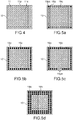
- the cavities 11 can be arranged in a matrix manner ( figure 4 ).
- matrix arrangement is understood to mean a periodic and regular arrangement in two orthogonal directions of cavities 11.
- the matrix arrangement notably comprises n rows and m columns of cavities 11.
- the method according to the present invention also comprises a step b) of forming membranes.
- Step b) of forming membranes 19 comprises in particular the transfer of a covering film 16 on the front face of the support substrate 10.
- the membranes 19 are suspended above the cavities 11.
- the transfer of the covering film may in particular involve a step b1) of bonding a substrate, said donor substrate 17, on the front face 11a, and a step b2) of removing a first part 17a of the donor substrate 17 so donkey keep that a second part 17a of said substrate forming the covering film 16 ( figure 1b, 1c, 2a, 2b, 2c , 3f and 3g ).
- step b1) of bonding can comprise molecular bonding (or direct), bonding by thermocompression.
- the invention should not however be limited to these two types of bonding, and may in particular comprise a bonding involving an intermediate bonding layer (for example a polymer material), an anodic bonding, an eutectic bonding.
- an intermediate bonding layer for example a polymer material
- the bonding step b1) can also be carried out under vacuum or under a controlled atmosphere, in particular to impose a predetermined gas and pressure in the cavities 11 sealed by the covering film 16.
- the sealing of the cavities by the covering film is hermetic.
- hermetic seal is meant a seal which prevents gas exchange between the cavities in question and the external environment.
- Step b1) can be preceded by a step of forming a weakening zone 17c separating the first part 17a from the second part 17b, and at which a fracture of the donor substrate 17 is likely to occur, during of the execution of step b2), under the effect of a heat treatment and / or a mechanical action.
- the weakening zone 17c can be an amorphous zone or an implanted zone, in particular a zone implanted with hydrogen atoms.
- step b2) can include a mechanical thinning step ( figures 2a to 2c ), and in particular a step of mechanical thinning by abrasion (“Grinding” according to Anglo-Saxon terminology) optionally supplemented by chemical etching.
- the first part 17a and the second part 17b are separated by a stopper layer 17d at which the chemical etching of step b2) stops.
- chemical etching is etching selective, and preferably etches the first part 17a with regard to the stop layer 17d.
- the donor substrate 17, according to this alternative, can in particular be a silicon-on-insulator (“SOI”) substrate, the insulating layer being the barrier layer.
- SOI silicon-on-insulator
- the silicon layer of the SOI substrate is advantageously heavily doped.
- the stop layer can be etched by abrasion or by a selective chemical etching step.
- Step b) can be preceded by a step of depositing a passivation layer covering the front face 10a ( figure 3e ).
- the passivation layer 18 may in particular comprise a first deposit of a layer of silicon nitride 18a followed by a second deposit of a layer of silicon dioxide 18b.
- each of these two layers 18a and 18b can be between 30 nm and 300 nm.
- the first layer 18a can be formed by low pressure chemical vapor deposition (“LPCVD” or “Low Pressure Chemical Vapor Deposition” according to Anglo-Saxon terminology).
- LPCVD low pressure chemical vapor deposition
- Low Pressure Chemical Vapor Deposition Low Pressure Chemical Vapor Deposition
- the second layer 18b can be formed by plasma-assisted chemical vapor deposition.
- Step b) can also be followed by a step of depositing a passivation layer 20 on the cover film ( figure 3h ).
- the passivation layer 20 may comprise a layer of silicon nitride 50 nm thick, and formed by LPCVD.
- central resonators formed by central cavities 11c and central membranes 19c on the one hand
- peripheral resonators formed by peripheral cavities 11p and peripheral membranes 19p on the other hand.
- the peripheral resonators are arranged around the assembly formed by the central resonators.
- arranged around is meant forming a closed path around the central resonators.
- the peripheral membranes 19p can comprise the membranes at the edge of the matrix arrangement ( figure 5b ).
- peripheral membranes 19p form an outline of several membranes of width ( figure 5d ).
- the peripheral membranes are, at least in part, removed during a withdrawal step c) carried out after step b).
- Step c) can comprise a localized etching of the covering film, the localized etching comprises in particular a wet etching or a dry etching.
- peripheral membranes 19p are removed during step c). According to this variant, it can be considered to keep at least two adjacent peripheral membranes denoted 19pa ( figure 5c ).
- Step c) of removing the peripheral membranes is also illustrated in figure 3i .
- This removal can in particular take place during a localized etching step of the passivation layer 20, and of the covering film 16 intended to give access to the contact zones 14.
- a contacting step can finally be carried out ( figure 3j ) at the level of the contact zone 14, and at the level of the central membranes.
- This step may in particular involve the formation of openings in the passivation layers 18 and 20, and the formation of contacts 14a and 21, in particular by depositing silicon aluminide by physical vapor deposition.
- the contacts 14 can contact all or part of the membranes 19. All of the membranes 19 can be provided with one or more groups of membranes 19, the contacts 14 of the membranes 19 of a given group forming a common electrode.
- the contacts 14, as soon as they form a common electrode, can be arranged in lines, spirals.
- the invention is not limited to these configurations alone.
- the method of manufacturing a plurality of resonators according to the present invention, and in particular the removal of at least part of the peripheral membranes, makes it possible to increase the quality factor of the resonator.
- the inventors are of the opinion that, in particular during the execution of the bonding step, the pressure in the cavities is different from one cavity to another and consequently induces a deflection of the membranes of a resonator to the other. This difference is notably more marked between the central cavities and the peripheral cavities.
- peripheral membranes as defined in the present invention, and more particularly those closest to the edge of the plurality of membranes are subjected to very stresses (for example due to the internal pressure of the cavity). different from those experienced by the central membranes.
- the central resonators form a more homogeneous set in terms of the stresses undergone, and therefore collectively present a quality factor greater than the quality factor of the same set and for which all the central and peripheral membranes are preserved.
- the improvement in the quality factor then makes it possible to consider the manufacture of gas sensors by gravimetric measurement having better sensitivity.
- Such sensors can in particular be used as odor sensors or else for mass spectroscopy.
- the senor can comprise a capacitive ultrasound micro-transducer (“cMUT” or “capacitive micromachined ultrasound transducer” according to Anglo-Saxon terminology).
- cMUT capacitive ultrasound micro-transducer
- Capacitive micromachined ultrasound transducer according to Anglo-Saxon terminology
Landscapes
- Engineering & Computer Science (AREA)
- Microelectronics & Electronic Packaging (AREA)
- Manufacturing & Machinery (AREA)
- Chemical & Material Sciences (AREA)
- Analytical Chemistry (AREA)
- Physics & Mathematics (AREA)
- Pathology (AREA)
- General Health & Medical Sciences (AREA)
- General Physics & Mathematics (AREA)
- Immunology (AREA)
- Biochemistry (AREA)
- Life Sciences & Earth Sciences (AREA)
- Health & Medical Sciences (AREA)
- Computer Hardware Design (AREA)
- Acoustics & Sound (AREA)
- Micromachines (AREA)
- Piezo-Electric Or Mechanical Vibrators, Or Delay Or Filter Circuits (AREA)
- Pressure Sensors (AREA)
Applications Claiming Priority (1)
| Application Number | Priority Date | Filing Date | Title |
|---|---|---|---|
| FR1906057A FR3097052B1 (fr) | 2019-06-07 | 2019-06-07 | Procédé de fabrication d’une pluralité de résonateurs |
Publications (2)
| Publication Number | Publication Date |
|---|---|
| EP3748352A1 true EP3748352A1 (de) | 2020-12-09 |
| EP3748352B1 EP3748352B1 (de) | 2022-12-14 |
Family
ID=68581863
Family Applications (1)
| Application Number | Title | Priority Date | Filing Date |
|---|---|---|---|
| EP20178063.2A Active EP3748352B1 (de) | 2019-06-07 | 2020-06-03 | Herstellungsverfahren einer vielzahl von resonatoren |
Country Status (3)
| Country | Link |
|---|---|
| US (1) | US11584639B2 (de) |
| EP (1) | EP3748352B1 (de) |
| FR (1) | FR3097052B1 (de) |
Families Citing this family (2)
| Publication number | Priority date | Publication date | Assignee | Title |
|---|---|---|---|---|
| FR3077163B1 (fr) * | 2018-01-22 | 2021-08-27 | Soitec Silicon On Insulator | Procedes de conception et de fabrication d'un dispositif comprenant un reseau d'elements micro-usines, dispositif obtenu a l'issu de tels procedes |
| US20230372970A1 (en) * | 2022-05-18 | 2023-11-23 | Taiwan Semiconductor Manufacturing Co., Ltd. | Transducer device and method of manufacture |
Citations (5)
| Publication number | Priority date | Publication date | Assignee | Title |
|---|---|---|---|---|
| EP2152024A1 (de) | 2007-04-27 | 2010-02-10 | Hitachi Ltd. | Ultraschallwandler und ultraschall-bildgebervorrichtung |
| WO2010073534A1 (en) * | 2008-12-25 | 2010-07-01 | Canon Kabushiki Kaisha | Electromechanical transducer and production method therefor |
| US20130128702A1 (en) * | 2011-05-12 | 2013-05-23 | Georgia Tech Research Corporation | Compact, energy-efficient ultrasound imaging probes using cmut arrays with integrated electronics |
| US20170245035A1 (en) | 2014-09-17 | 2017-08-24 | Intel Corporation | DIE WITH INTEGRATED MICROPHONE DEVICE USING THROUGH-SILICON VIAS (TSVs) |
| EP3424603A1 (de) | 2017-07-07 | 2019-01-09 | Konica Minolta, Inc. | Verfahren zur herstellung eines mems-wandlers, mems-wandler, ultraschallsonde und ultraschalldiagnosevorrichtung |
Family Cites Families (3)
| Publication number | Priority date | Publication date | Assignee | Title |
|---|---|---|---|---|
| US20080121042A1 (en) * | 2006-11-27 | 2008-05-29 | Bioscale, Inc. | Fluid paths in etchable materials |
| EP3169449B1 (de) * | 2014-07-16 | 2018-03-21 | Koninklijke Philips N.V. | Modulare cmut-matrizen mit gleichförmigem abstand |
| WO2021237043A1 (en) * | 2020-05-22 | 2021-11-25 | Bfly Operations, Inc. | Ultrasonic transducer array having varying cavity diameter profile |
-
2019
- 2019-06-07 FR FR1906057A patent/FR3097052B1/fr active Active
-
2020
- 2020-06-03 US US16/891,340 patent/US11584639B2/en active Active
- 2020-06-03 EP EP20178063.2A patent/EP3748352B1/de active Active
Patent Citations (5)
| Publication number | Priority date | Publication date | Assignee | Title |
|---|---|---|---|---|
| EP2152024A1 (de) | 2007-04-27 | 2010-02-10 | Hitachi Ltd. | Ultraschallwandler und ultraschall-bildgebervorrichtung |
| WO2010073534A1 (en) * | 2008-12-25 | 2010-07-01 | Canon Kabushiki Kaisha | Electromechanical transducer and production method therefor |
| US20130128702A1 (en) * | 2011-05-12 | 2013-05-23 | Georgia Tech Research Corporation | Compact, energy-efficient ultrasound imaging probes using cmut arrays with integrated electronics |
| US20170245035A1 (en) | 2014-09-17 | 2017-08-24 | Intel Corporation | DIE WITH INTEGRATED MICROPHONE DEVICE USING THROUGH-SILICON VIAS (TSVs) |
| EP3424603A1 (de) | 2017-07-07 | 2019-01-09 | Konica Minolta, Inc. | Verfahren zur herstellung eines mems-wandlers, mems-wandler, ultraschallsonde und ultraschalldiagnosevorrichtung |
Non-Patent Citations (2)
| Title |
|---|
| HYUNJOO J. LEE ET AL.: "CMUT as a Chemical Sensor for DMMP Detection", 2008, IEEE, pages: 434 - 439 |
| S. FANGET ET AL.: "Gas sensors based on gravimétrie detection-A review", SENSORS AND ACTUATORS B, vol. 160, 2011, pages 804 - 821 |
Also Published As
| Publication number | Publication date |
|---|---|
| US20200385262A1 (en) | 2020-12-10 |
| US11584639B2 (en) | 2023-02-21 |
| EP3748352B1 (de) | 2022-12-14 |
| FR3097052B1 (fr) | 2021-07-02 |
| FR3097052A1 (fr) | 2020-12-11 |
Similar Documents
| Publication | Publication Date | Title |
|---|---|---|
| EP0605302B1 (de) | Herstellungsverfahren für Druckwandler mittels der Silicium auf Isolation Technologie sowie derart hergestellte Wandler | |
| EP3859800B1 (de) | Hybridstruktur für vorrichtung mit oberflächenschallwellen | |
| EP1840582B1 (de) | Resonanter Trägheitsmikrosensor variabler Dicke, der im Bereich der Oberflächentechnologien eingesetzt wird | |
| EP0754953B1 (de) | Verfahren zur Herstellung einer Struktur mit einer mittels Anschlägen auf Abstand von einem Substrat gehaltenen Nutzschicht, sowie Verfahren zur Loslösung einer solchen Schicht | |
| WO2019129979A1 (fr) | Procede de realisation d'un resonateur acoustique a ondes de volume a capacite parasite reduite | |
| FR2925038A1 (fr) | Systeme micromecanique et procede de realisation | |
| EP3975584B1 (de) | Verfahren zur herstellung eines elektroakustischen transducers | |
| EP1155442A1 (de) | Mehrschichtige strukturen mit kontrollierten eigenspannungen und verfahren zur herstellung derselben | |
| EP2144369A1 (de) | Volumenwellenresonator | |
| EP2520900B1 (de) | Gyroskop mit reduzierter parasitärer Kapazität | |
| EP3748352B1 (de) | Herstellungsverfahren einer vielzahl von resonatoren | |
| EP3556114B1 (de) | Akustische mikroelektronische vorrichtung | |
| WO2005061374A1 (fr) | Microcomposant comportant une microcavite hermetique et procede de fabrication d'un tel microcomposant | |
| EP2414276B1 (de) | Herstellung einer ein nems-bauteil aus monokristallinem silizium und einen transistor umfassenden mikroelektronischen vorrichtung, dessen gate in der gleichen schicht wie die bewegliche struktur des bauteils hergestellt ist | |
| EP2949621B1 (de) | Kapazitive mikro- und/ oder nanoelektronische Vorrichtung mit erhöhter Kompaktheit | |
| EP4017832A1 (de) | Verfahren zur abdichtung von hohlräumen mittels membranen | |
| EP3975588B1 (de) | Verfahren zur herstellung eines elektroakustischen transducers | |
| EP3490928B1 (de) | Resonanter chemischer sensor mit einer funktionalisierungsvorrichtung und verfahren zur herstellung davon | |
| FR3097091A1 (fr) | dispositif pourvu d’une pluralité de résonateurs présentant collectivement un facteur de qualité amélioré | |
| EP0864093A1 (de) | Sensor, insbesondere akzelerometer, stellglied und herstellungsverfahren für eine sensor- oder stellgliedstruktur mit stellenweiser elektrischer isolation | |
| EP3944322B1 (de) | Verfahren zur herstellung einer mikroelektronischen vorrichtung | |
| EP4627303A1 (de) | Vorrichtung zur detektion elektromagnetischer strahlung und herstellungsverfahren | |
| EP2747190B1 (de) | Kapazitive Mems-Komponente mit Erdübertragungslinie | |
| FR2973608A1 (fr) | Procede d'ajustement de la frequence de resonance d'un element vibrant micro-usine | |
| EP3386910A1 (de) | Verfahren zur herstellung einer mikroelektromechanischen vorrichtung und zugehörige vorrichtung |
Legal Events
| Date | Code | Title | Description |
|---|---|---|---|
| PUAI | Public reference made under article 153(3) epc to a published international application that has entered the european phase |
Free format text: ORIGINAL CODE: 0009012 |
|
| STAA | Information on the status of an ep patent application or granted ep patent |
Free format text: STATUS: REQUEST FOR EXAMINATION WAS MADE |
|
| 17P | Request for examination filed |
Effective date: 20200603 |
|
| AK | Designated contracting states |
Kind code of ref document: A1 Designated state(s): AL AT BE BG CH CY CZ DE DK EE ES FI FR GB GR HR HU IE IS IT LI LT LU LV MC MK MT NL NO PL PT RO RS SE SI SK SM TR |
|
| AX | Request for extension of the european patent |
Extension state: BA ME |
|
| GRAP | Despatch of communication of intention to grant a patent |
Free format text: ORIGINAL CODE: EPIDOSNIGR1 |
|
| STAA | Information on the status of an ep patent application or granted ep patent |
Free format text: STATUS: GRANT OF PATENT IS INTENDED |
|
| INTG | Intention to grant announced |
Effective date: 20220707 |
|
| GRAS | Grant fee paid |
Free format text: ORIGINAL CODE: EPIDOSNIGR3 |
|
| GRAA | (expected) grant |
Free format text: ORIGINAL CODE: 0009210 |
|
| STAA | Information on the status of an ep patent application or granted ep patent |
Free format text: STATUS: THE PATENT HAS BEEN GRANTED |
|
| AK | Designated contracting states |
Kind code of ref document: B1 Designated state(s): AL AT BE BG CH CY CZ DE DK EE ES FI FR GB GR HR HU IE IS IT LI LT LU LV MC MK MT NL NO PL PT RO RS SE SI SK SM TR |
|
| REG | Reference to a national code |
Ref country code: GB Ref legal event code: FG4D Free format text: NOT ENGLISH |
|
| REG | Reference to a national code |
Ref country code: CH Ref legal event code: EP |
|
| REG | Reference to a national code |
Ref country code: DE Ref legal event code: R096 Ref document number: 602020006874 Country of ref document: DE |
|
| REG | Reference to a national code |
Ref country code: IE Ref legal event code: FG4D Free format text: LANGUAGE OF EP DOCUMENT: FRENCH |
|
| REG | Reference to a national code |
Ref country code: AT Ref legal event code: REF Ref document number: 1537973 Country of ref document: AT Kind code of ref document: T Effective date: 20230115 |
|
| REG | Reference to a national code |
Ref country code: LT Ref legal event code: MG9D |
|
| REG | Reference to a national code |
Ref country code: NL Ref legal event code: MP Effective date: 20221214 |
|
| PG25 | Lapsed in a contracting state [announced via postgrant information from national office to epo] |
Ref country code: SE Free format text: LAPSE BECAUSE OF FAILURE TO SUBMIT A TRANSLATION OF THE DESCRIPTION OR TO PAY THE FEE WITHIN THE PRESCRIBED TIME-LIMIT Effective date: 20221214 Ref country code: NO Free format text: LAPSE BECAUSE OF FAILURE TO SUBMIT A TRANSLATION OF THE DESCRIPTION OR TO PAY THE FEE WITHIN THE PRESCRIBED TIME-LIMIT Effective date: 20230314 Ref country code: LT Free format text: LAPSE BECAUSE OF FAILURE TO SUBMIT A TRANSLATION OF THE DESCRIPTION OR TO PAY THE FEE WITHIN THE PRESCRIBED TIME-LIMIT Effective date: 20221214 Ref country code: FI Free format text: LAPSE BECAUSE OF FAILURE TO SUBMIT A TRANSLATION OF THE DESCRIPTION OR TO PAY THE FEE WITHIN THE PRESCRIBED TIME-LIMIT Effective date: 20221214 |
|
| REG | Reference to a national code |
Ref country code: AT Ref legal event code: MK05 Ref document number: 1537973 Country of ref document: AT Kind code of ref document: T Effective date: 20221214 |
|
| PG25 | Lapsed in a contracting state [announced via postgrant information from national office to epo] |
Ref country code: RS Free format text: LAPSE BECAUSE OF FAILURE TO SUBMIT A TRANSLATION OF THE DESCRIPTION OR TO PAY THE FEE WITHIN THE PRESCRIBED TIME-LIMIT Effective date: 20221214 Ref country code: LV Free format text: LAPSE BECAUSE OF FAILURE TO SUBMIT A TRANSLATION OF THE DESCRIPTION OR TO PAY THE FEE WITHIN THE PRESCRIBED TIME-LIMIT Effective date: 20221214 Ref country code: HR Free format text: LAPSE BECAUSE OF FAILURE TO SUBMIT A TRANSLATION OF THE DESCRIPTION OR TO PAY THE FEE WITHIN THE PRESCRIBED TIME-LIMIT Effective date: 20221214 Ref country code: GR Free format text: LAPSE BECAUSE OF FAILURE TO SUBMIT A TRANSLATION OF THE DESCRIPTION OR TO PAY THE FEE WITHIN THE PRESCRIBED TIME-LIMIT Effective date: 20230315 |
|
| PG25 | Lapsed in a contracting state [announced via postgrant information from national office to epo] |
Ref country code: NL Free format text: LAPSE BECAUSE OF FAILURE TO SUBMIT A TRANSLATION OF THE DESCRIPTION OR TO PAY THE FEE WITHIN THE PRESCRIBED TIME-LIMIT Effective date: 20221214 |
|
| PG25 | Lapsed in a contracting state [announced via postgrant information from national office to epo] |
Ref country code: SM Free format text: LAPSE BECAUSE OF FAILURE TO SUBMIT A TRANSLATION OF THE DESCRIPTION OR TO PAY THE FEE WITHIN THE PRESCRIBED TIME-LIMIT Effective date: 20221214 Ref country code: RO Free format text: LAPSE BECAUSE OF FAILURE TO SUBMIT A TRANSLATION OF THE DESCRIPTION OR TO PAY THE FEE WITHIN THE PRESCRIBED TIME-LIMIT Effective date: 20221214 Ref country code: PT Free format text: LAPSE BECAUSE OF FAILURE TO SUBMIT A TRANSLATION OF THE DESCRIPTION OR TO PAY THE FEE WITHIN THE PRESCRIBED TIME-LIMIT Effective date: 20230414 Ref country code: ES Free format text: LAPSE BECAUSE OF FAILURE TO SUBMIT A TRANSLATION OF THE DESCRIPTION OR TO PAY THE FEE WITHIN THE PRESCRIBED TIME-LIMIT Effective date: 20221214 Ref country code: EE Free format text: LAPSE BECAUSE OF FAILURE TO SUBMIT A TRANSLATION OF THE DESCRIPTION OR TO PAY THE FEE WITHIN THE PRESCRIBED TIME-LIMIT Effective date: 20221214 Ref country code: CZ Free format text: LAPSE BECAUSE OF FAILURE TO SUBMIT A TRANSLATION OF THE DESCRIPTION OR TO PAY THE FEE WITHIN THE PRESCRIBED TIME-LIMIT Effective date: 20221214 Ref country code: AT Free format text: LAPSE BECAUSE OF FAILURE TO SUBMIT A TRANSLATION OF THE DESCRIPTION OR TO PAY THE FEE WITHIN THE PRESCRIBED TIME-LIMIT Effective date: 20221214 |
|
| PG25 | Lapsed in a contracting state [announced via postgrant information from national office to epo] |
Ref country code: SK Free format text: LAPSE BECAUSE OF FAILURE TO SUBMIT A TRANSLATION OF THE DESCRIPTION OR TO PAY THE FEE WITHIN THE PRESCRIBED TIME-LIMIT Effective date: 20221214 Ref country code: PL Free format text: LAPSE BECAUSE OF FAILURE TO SUBMIT A TRANSLATION OF THE DESCRIPTION OR TO PAY THE FEE WITHIN THE PRESCRIBED TIME-LIMIT Effective date: 20221214 Ref country code: IS Free format text: LAPSE BECAUSE OF FAILURE TO SUBMIT A TRANSLATION OF THE DESCRIPTION OR TO PAY THE FEE WITHIN THE PRESCRIBED TIME-LIMIT Effective date: 20230414 Ref country code: AL Free format text: LAPSE BECAUSE OF FAILURE TO SUBMIT A TRANSLATION OF THE DESCRIPTION OR TO PAY THE FEE WITHIN THE PRESCRIBED TIME-LIMIT Effective date: 20221214 |
|
| REG | Reference to a national code |
Ref country code: DE Ref legal event code: R097 Ref document number: 602020006874 Country of ref document: DE |
|
| PLBE | No opposition filed within time limit |
Free format text: ORIGINAL CODE: 0009261 |
|
| STAA | Information on the status of an ep patent application or granted ep patent |
Free format text: STATUS: NO OPPOSITION FILED WITHIN TIME LIMIT |
|
| PG25 | Lapsed in a contracting state [announced via postgrant information from national office to epo] |
Ref country code: DK Free format text: LAPSE BECAUSE OF FAILURE TO SUBMIT A TRANSLATION OF THE DESCRIPTION OR TO PAY THE FEE WITHIN THE PRESCRIBED TIME-LIMIT Effective date: 20221214 |
|
| 26N | No opposition filed |
Effective date: 20230915 |
|
| PG25 | Lapsed in a contracting state [announced via postgrant information from national office to epo] |
Ref country code: SI Free format text: LAPSE BECAUSE OF FAILURE TO SUBMIT A TRANSLATION OF THE DESCRIPTION OR TO PAY THE FEE WITHIN THE PRESCRIBED TIME-LIMIT Effective date: 20221214 |
|
| PG25 | Lapsed in a contracting state [announced via postgrant information from national office to epo] |
Ref country code: MC Free format text: LAPSE BECAUSE OF FAILURE TO SUBMIT A TRANSLATION OF THE DESCRIPTION OR TO PAY THE FEE WITHIN THE PRESCRIBED TIME-LIMIT Effective date: 20221214 |
|
| PG25 | Lapsed in a contracting state [announced via postgrant information from national office to epo] |
Ref country code: MC Free format text: LAPSE BECAUSE OF FAILURE TO SUBMIT A TRANSLATION OF THE DESCRIPTION OR TO PAY THE FEE WITHIN THE PRESCRIBED TIME-LIMIT Effective date: 20221214 |
|
| REG | Reference to a national code |
Ref country code: CH Ref legal event code: PL |
|
| REG | Reference to a national code |
Ref country code: BE Ref legal event code: MM Effective date: 20230630 |
|
| PG25 | Lapsed in a contracting state [announced via postgrant information from national office to epo] |
Ref country code: LU Free format text: LAPSE BECAUSE OF NON-PAYMENT OF DUE FEES Effective date: 20230603 |
|
| REG | Reference to a national code |
Ref country code: IE Ref legal event code: MM4A |
|
| PG25 | Lapsed in a contracting state [announced via postgrant information from national office to epo] |
Ref country code: LU Free format text: LAPSE BECAUSE OF NON-PAYMENT OF DUE FEES Effective date: 20230603 |
|
| PG25 | Lapsed in a contracting state [announced via postgrant information from national office to epo] |
Ref country code: IE Free format text: LAPSE BECAUSE OF NON-PAYMENT OF DUE FEES Effective date: 20230603 |
|
| PG25 | Lapsed in a contracting state [announced via postgrant information from national office to epo] |
Ref country code: IE Free format text: LAPSE BECAUSE OF NON-PAYMENT OF DUE FEES Effective date: 20230603 Ref country code: CH Free format text: LAPSE BECAUSE OF NON-PAYMENT OF DUE FEES Effective date: 20230630 |
|
| PG25 | Lapsed in a contracting state [announced via postgrant information from national office to epo] |
Ref country code: BE Free format text: LAPSE BECAUSE OF NON-PAYMENT OF DUE FEES Effective date: 20230630 |
|
| PG25 | Lapsed in a contracting state [announced via postgrant information from national office to epo] |
Ref country code: BG Free format text: LAPSE BECAUSE OF FAILURE TO SUBMIT A TRANSLATION OF THE DESCRIPTION OR TO PAY THE FEE WITHIN THE PRESCRIBED TIME-LIMIT Effective date: 20221214 |
|
| PG25 | Lapsed in a contracting state [announced via postgrant information from national office to epo] |
Ref country code: BG Free format text: LAPSE BECAUSE OF FAILURE TO SUBMIT A TRANSLATION OF THE DESCRIPTION OR TO PAY THE FEE WITHIN THE PRESCRIBED TIME-LIMIT Effective date: 20221214 |
|
| PGFP | Annual fee paid to national office [announced via postgrant information from national office to epo] |
Ref country code: DE Payment date: 20250618 Year of fee payment: 6 |
|
| PGFP | Annual fee paid to national office [announced via postgrant information from national office to epo] |
Ref country code: GB Payment date: 20250625 Year of fee payment: 6 |
|
| PGFP | Annual fee paid to national office [announced via postgrant information from national office to epo] |
Ref country code: FR Payment date: 20250623 Year of fee payment: 6 |
|
| PG25 | Lapsed in a contracting state [announced via postgrant information from national office to epo] |
Ref country code: CY Free format text: LAPSE BECAUSE OF FAILURE TO SUBMIT A TRANSLATION OF THE DESCRIPTION OR TO PAY THE FEE WITHIN THE PRESCRIBED TIME-LIMIT; INVALID AB INITIO Effective date: 20200603 |
|
| PG25 | Lapsed in a contracting state [announced via postgrant information from national office to epo] |
Ref country code: HU Free format text: LAPSE BECAUSE OF FAILURE TO SUBMIT A TRANSLATION OF THE DESCRIPTION OR TO PAY THE FEE WITHIN THE PRESCRIBED TIME-LIMIT; INVALID AB INITIO Effective date: 20200603 |
|
| PGFP | Annual fee paid to national office [announced via postgrant information from national office to epo] |
Ref country code: IT Payment date: 20250630 Year of fee payment: 6 |
|
| PG25 | Lapsed in a contracting state [announced via postgrant information from national office to epo] |
Ref country code: TR Free format text: LAPSE BECAUSE OF FAILURE TO SUBMIT A TRANSLATION OF THE DESCRIPTION OR TO PAY THE FEE WITHIN THE PRESCRIBED TIME-LIMIT Effective date: 20221214 |