EP3748322A1 - Sensor chip and force sensor device - Google Patents
Sensor chip and force sensor device Download PDFInfo
- Publication number
- EP3748322A1 EP3748322A1 EP19743214.9A EP19743214A EP3748322A1 EP 3748322 A1 EP3748322 A1 EP 3748322A1 EP 19743214 A EP19743214 A EP 19743214A EP 3748322 A1 EP3748322 A1 EP 3748322A1
- Authority
- EP
- European Patent Office
- Prior art keywords
- detecting
- beams
- sensor chip
- disposed
- force
- Prior art date
- Legal status (The legal status is an assumption and is not a legal conclusion. Google has not performed a legal analysis and makes no representation as to the accuracy of the status listed.)
- Granted
Links
Images







Classifications
-
- G—PHYSICS
- G01—MEASURING; TESTING
- G01L—MEASURING FORCE, STRESS, TORQUE, WORK, MECHANICAL POWER, MECHANICAL EFFICIENCY, OR FLUID PRESSURE
- G01L1/00—Measuring force or stress, in general
- G01L1/18—Measuring force or stress, in general using properties of piezo-resistive materials, i.e. materials of which the ohmic resistance varies according to changes in magnitude or direction of force applied to the material
-
- G—PHYSICS
- G01—MEASURING; TESTING
- G01L—MEASURING FORCE, STRESS, TORQUE, WORK, MECHANICAL POWER, MECHANICAL EFFICIENCY, OR FLUID PRESSURE
- G01L1/00—Measuring force or stress, in general
- G01L1/20—Measuring force or stress, in general by measuring variations in ohmic resistance of solid materials or of electrically-conductive fluids; by making use of electrokinetic cells, i.e. liquid-containing cells wherein an electrical potential is produced or varied upon the application of stress
- G01L1/22—Measuring force or stress, in general by measuring variations in ohmic resistance of solid materials or of electrically-conductive fluids; by making use of electrokinetic cells, i.e. liquid-containing cells wherein an electrical potential is produced or varied upon the application of stress using resistance strain gauges
- G01L1/2206—Special supports with preselected places to mount the resistance strain gauges; Mounting of supports
-
- G—PHYSICS
- G01—MEASURING; TESTING
- G01L—MEASURING FORCE, STRESS, TORQUE, WORK, MECHANICAL POWER, MECHANICAL EFFICIENCY, OR FLUID PRESSURE
- G01L1/00—Measuring force or stress, in general
- G01L1/20—Measuring force or stress, in general by measuring variations in ohmic resistance of solid materials or of electrically-conductive fluids; by making use of electrokinetic cells, i.e. liquid-containing cells wherein an electrical potential is produced or varied upon the application of stress
- G01L1/22—Measuring force or stress, in general by measuring variations in ohmic resistance of solid materials or of electrically-conductive fluids; by making use of electrokinetic cells, i.e. liquid-containing cells wherein an electrical potential is produced or varied upon the application of stress using resistance strain gauges
- G01L1/2287—Measuring force or stress, in general by measuring variations in ohmic resistance of solid materials or of electrically-conductive fluids; by making use of electrokinetic cells, i.e. liquid-containing cells wherein an electrical potential is produced or varied upon the application of stress using resistance strain gauges constructional details of the strain gauges
-
- G—PHYSICS
- G01—MEASURING; TESTING
- G01L—MEASURING FORCE, STRESS, TORQUE, WORK, MECHANICAL POWER, MECHANICAL EFFICIENCY, OR FLUID PRESSURE
- G01L5/00—Apparatus for, or methods of, measuring force, work, mechanical power, or torque, specially adapted for specific purposes
- G01L5/16—Apparatus for, or methods of, measuring force, work, mechanical power, or torque, specially adapted for specific purposes for measuring several components of force
- G01L5/161—Apparatus for, or methods of, measuring force, work, mechanical power, or torque, specially adapted for specific purposes for measuring several components of force using variations in ohmic resistance
- G01L5/162—Apparatus for, or methods of, measuring force, work, mechanical power, or torque, specially adapted for specific purposes for measuring several components of force using variations in ohmic resistance of piezoresistors
Definitions
- the present invention relates to a sensor chip and a force sensor device.
- a force sensor device has been known in which a plurality of strain gauges is applied to a strain generator made from a metal, and a strain caused when an external force is applied is converted into an electric signal, thereby detecting a multi-axis direction force.
- this force sensor device has problems in accuracy and productivity because it is necessary to attach strain gauges one by one manually, and it is difficult to downsize the device due to its structure.
- a force sensor device has been proposed in which a strain gauge is replaced with a MEMS sensor chip for a strain detection to solve a problem of lamination accuracy and to achieve miniaturization (see, for example, PTL 1).
- the force sensor can perform a high accuracy.
- the input is a composite input (when the input is a composite input along any two or more of the six axes [Fx, Fy, Fz, Mx, My, Mz]), an error of the force sensor is increased due to an insufficient axial separation property, and the accuracy is reduced.
- the composite input there are combinations of axes of the composite input that does not satisfy an accuracy target value.
- the present invention has been made in view of the above, and is intended to improve the axial separation property and a sensor accuracy for the composite input of the sensor chip.
- the present sensor chip (110) includes a substrate, first supporting portions (111a, 111b, 111c, 111d), a second supporting portion (111e) around which the first support portions are disposed, the second supporting portion being disposed at a center of the substrate, first detecting beams (113a, 113d, 113g, 113j) each connecting the first supporting portions, which are mutually adjacent, second detecting beams (113b, 113e, 113h, 113k) disposed in parallel with the first detecting beams between the first detecting beams and the second supporting portion, force points (114a, 114b, 114c, 114d) disposed in the first detecting beams so as to be applied with force, and a plurality of strain detecting elements disposed a predetermined positions of the first detecting beams and the second detecting beams, wherein the plurality of strain detecting elements includes a first detecting portion having a strain detecting element capable of detecting force in a first direction, and a second detecting portion having
- the disclosed technique can improve an axial separation property and a sensor accuracy for a composite input of a sensor chip.
- FIG. 1 is perspective views illustrating a force sensor device according to a first embodiment.
- FIG. 2 is a perspective view illustrating a sensor chip and a strain generator of a force sensor device according to a first embodiment.
- the force sensor device 1 includes a sensor chip 110, a strain generator 20, and an input/output board 30.
- the force sensor device 1 is, for example, a multi-axis force sensor device mounted on an arm or a finger of a robot used for a machine tool or the like.
- the sensor chip 110 has function of detecting a displacement along predetermined axial directions of up to six axes.
- the strain generator 20 has the function of transferring applied force to the sensor chip 110.
- the sensor chip 110 is bonded to the upper surface side of the strain generator 20 so as not to protrude from the strain generator 20. Also, one end side of the input/output board 30 for providing an input/output signals to and from the sensor chip 110 is appropriately bent on the upper surface and each side of the strain generator 20. Each electrode 31 of the sensor chip 110 and the input/output board 30 is electrically connected by a bonding wire (not illustrated) or the like.
- an active component 32 and a passive component 39 are mounted in a region disposed on the first side of the strain generator 20.
- an active component 33 and a passive component 39 are mounted in a region disposed on the second side of the strain generator 20.
- an active component 34 and the passive component 39 are mounted in a region disposed on the third side of the strain generator 20.
- the active component 35 and the passive component 39 are mounted in a region disposed on the fourth side of the strain generator 20.
- the active component 33 is, for example, an IC (AD converter) that converts an analog electric signal from a bridge circuit that detects an X-axis direction force Fx output from the sensor chip 110 and an analog electric signal from a bridge circuit that detects a Y-axis direction force Fy output from the sensor chip 110 into a digital electric signal.
- the active component 34 is, for example, an IC (AD converter) that converts an analog electric signal from a bridge circuit that detects a Z-axis direction force Fz output from the sensor chip 110 and an analog electric signal from a bridge circuit that detects a moment Mx that rotates around the X-axis output from the sensor chip 110 as an axis to a digital electric signal.
- AD converter AD converter
- the active component 35 is, for example, an IC (AD converter) that converts an analog electric signal from a bridge circuit that detects a moment My that rotates around the Y-axis as an axis output from the sensor chip 110 and an analog electric signal from a bridge circuit that detects a moment Mz that rotates around the Z-axis as an axis output from the sensor chip 110 into a digital electric signal.
- AD converter AD converter
- the active component 32 is, for example, an IC that performs predetermined calculation on digital electric signals output from active components 33, 34, and 35 to generate and output signals indicative of forces Fx, Fy, and Fz as well as moments Mx, My, and Mz.
- a passive component 39 may be a resistor, capacitor, or the like, connected to the active components 32-35.
- the active components 32 to 35 may be mounted on the external circuit side connected to the input/output board 30 without mounting the active components 32 to 35 on the input/output board 30. In this case, an analog electric signal is output from the input/output board 30.
- the input/output board 30 is bent to direct an outside below the first side surface of the strain generator 20 and the other end of the input/output board 30 is drawn outwardly.
- a terminal (not illustrated) capable of electrical input/output with an external circuit (such as a control device) connected to the force sensor device 1 is arranged.
- the side on which the sensor chip 110 is provided is an upper side or one side, and the opposite side is a lower side or the other side.
- the side of each portion of the sensor chip 110 has one or a upper surface, and the other side has the other side or a bottom surface.
- the force sensor device 1 may be used in an inverted state or may be disposed at any angle.
- a plan view refers to viewing an object from the normal direction (Z-axis direction) of the upper surface of the sensor chip 110
- planar shape refers to viewing an object from the normal direction (Z-axis direction) of the upper surface of the sensor chip 110.
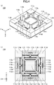
- FIG. 3 illustrates the sensor chip 110 viewed from the upper side in the Z-axis direction, in which (a) is a perspective view and (b) is a plan view.
- FIG. 4 illustrates the sensor chip 110 viewed from the lower side in the Z-axis direction, in which (a) is a perspective view and (b) is a bottom view. In (b) of FIG. 4 , for convenience, surfaces of the same height are indicated by the same texture.
- the direction parallel to one side of the upper surface of the sensor chip 110 is the X-axis direction
- the direction perpendicular to the one side is the Y-axis direction
- the thickness direction (the normal direction of the upper surface of the sensor chip 110) of the sensor chip 110 is the Z-axis direction.
- the X-axis direction, the Y-axis direction, and the Z-axis direction are orthogonal to one another.
- the sensor chip 110 illustrated in FIGS. 3 and 4 is a MEMS (Micro Electro Mechanical Systems) sensor chip capable of detecting up to six axes in one chip and is formed from a semiconductor substrate such as a SOI (Silicon On Insulator) substrate.
- the planar shape of the sensor chip 110 may be, for example, a square of about 3000 ⁇ m square.
- the sensor chip 110 includes five columnar supporting portions 111a-111e.
- the planar shape of the supporting portions 111a-111e may be, for example, a square of about 500 ⁇ m.
- the first supporting portions 111a-111d are disposed at four corners of the sensor chip 110.
- the supporting portion 111e which is a second supporting portion, is disposed at the center of the supporting portions 111a-111d.
- the support portions 111a-111e may be formed, for example, of an active layer, a BOX layer, and a supporting layer of an SOI substrate, each thickness being, for example, about 500 ⁇ m.
- a reinforcing beam 112a is provided between the supporting portion 111a and the supporting portion 111b to reinforce the structure of the supporting portion 111a and the supporting portion 111b fixed at both ends (connecting adjacent supporting portions).
- a reinforcing beam 112b is provided for reinforcing the structure of the supporting portion 111b and the supporting portion 111c (connecting adjacent supporting portions).
- a reinforcing beam 112c is provided for reinforcing the structure (connecting adjacent supporting portions) fixed at both ends to the supporting portion 111c and the supporting portion 111d.
- a reinforcing beam 112d is provided for reinforcing the structure of the supporting portion 111d and the supporting portion 111a (connecting adjacent supports to each other).
- the four reinforcing beam 112a, 112b, 112c, and 112d which are the first reinforcing beam, are formed as frames, and the corners forming the intersections of the respective reinforcing beam are formed as supporting portions 111b, 111c, 111d, and 111a.
- the inner corner of the supporting portion 111a and the corner of the supporting portion 111e facing thereto are connected by a reinforcing beam 112e for reinforcing the structure.
- the inner corner of the supporting portion 111b and the corner of the supporting portion 111e facing thereto are connected by a reinforcing beam 112f for reinforcing the structure.
- the inner corner of the supporting portion 111c and the corner of the supporting portion 111e facing thereto are connected by a reinforcing beam 112g for reinforcing the structure.
- the inner corner of the supporting portion 111d and the corner of the supporting portion 111e facing thereto are connected by a reinforcing beam 112h for reinforcing the structure.
- the second reinforcing beam i.e., the reinforcing beam 112e-112h, is disposed diagonally with respect to the X-axis direction (the Y-axis direction). That is, the reinforcing beams 112e-112h are disposed non-parallel to the reinforcing beams 112a, 112b, 112c, and 112d.
- the reinforcing beams 112a-112h can be formed, for example, from an active layer, a BOX layer, and a support layer each of an SOI substrate.
- the thickness (the width in the short-end direction width) of reinforcing beam 112a-112h may be, for example, about 140 ⁇ m.
- the upper surface of each of the reinforcing beam 112a-112h is arranged on the same plane as that of the upper surface of the supporting portion 111a-111e.
- the lower surfaces respectively of the reinforcing beams 112a-112h are recessed toward the upper surface side by several tens of micrometers from the lower surface of the supporting portions 111a-111e and the lower surfaces of the force points 114a-114d. This is to prevent the lower surfaces of the reinforcing beams 112a-112h from contacting the surface of the strain generator 20 when the sensor chip 110 is bonded to the strain generator 20.
- the rigidity of the sensor chip 110 in its entirety can be made high by disposing the reinforcing beam, which is formed to be thicker than the detecting beam for detecting distortion, in addition to the detecting beam.
- the reinforcing beam which is formed to be thicker than the detecting beam for detecting distortion, in addition to the detecting beam.
- the detecting beam 113a for detecting the distortion is provided for detecting distortion, both ends of which are fixed to the supporting portion 111a and the supporting portion 111b at predetermined intervals in parallel with the reinforcing beam 112a (connecting adjacent supporting portions to each other) .
- the detecting beam 113b is provided in parallel with the detecting beam 113a interposing a predetermined interval with the detecting beam 113a and the supporting portion 111e.
- the detecting beam 113b connects an end of the reinforcing beam 112e on the side of the supporting portion 111e with an end of the reinforcing beam 112f on the side of the supporting portion 111e.
- the generally central longitudinal portion of the detecting beam 113a and the longitudinally central portion of the opposing detecting beam 113b are coupled by a detecting beam 113c positioned perpendicular to the detecting beam 113a and the detecting beam 113b.
- a detecting beam 113d is disposed inside the reinforcing beam 112b between the supporting portion 111b and the supporting portion 111c for detecting distortion (mutually connecting adjacent supporting portions). Both ends of the detecting beam 113d are respectively fixed to the supporting portion 111b and the supporting portion 111c in parallel with the reinforcing beam 112b while interposing a predetermined interval.
- a detecting beam 113e is disposed in parallel with the detecting beam 113d while interposing a predetermined interval between the detecting beam 113d and the supporting portion 111e.
- the detecting beam 113e connects an end of the reinforcing beam 112f on the side of the supporting portion 111e with an end of the reinforcing beam 112g on the side of the supporting portion 111e.
- a substantially central portion in the longitudinal direction of the detecting beam 113d and a substantially central portion in the longitudinal direction of the detecting beam 113e facing the detecting beam 113d are connected by a detecting beam 113f disposed in perpendicular to the detecting beam 113d and the detecting beam 113e.
- a detecting beam 113g is disposed for detecting distortion, wherein both ends of the detecting beam 113g are fixed to the supporting portion 111c and the supporting portion 111d in parallel with the reinforcing beam 112c while interposing a predetermined interval between the detecting beam 113g and the reinforcing beam 112c (adjacent supporting portions are connected to each other).
- the detecting beam 113h is disposed in parallel with the detecting beam 113g while interposing a predetermined interval between the detecting beam 113h and the detecting beam 113g.
- the detecting beam 113h connects an end of the reinforcing beam 112g on the side of the supporting portion 111e with an end of the reinforcing beam 112h on the side of the supporting portion 111e.
- a substantially central portion in the longitudinal direction of the detecting beam 113g and a substantially central portion in the longitudinal direction of the detecting beam 113h facing the detecting beam 113g are connected by a detecting beam 113i disposed in perpendicular to the detecting beam 113g and the detecting beam 113h.
- a detecting beam 113j is disposed for detecting distortion, wherein both ends of the detecting beam 113j are fixed to the supporting portion 111d and the supporting portion 111a in parallel with the reinforcing beam 112d while interposing a predetermined interval between the detecting beam 113j and the reinforcing beam 112d (adjacent supporting portions are connected to each other).
- the detecting beam 113k is disposed in parallel with the detecting beam 113j while interposing a predetermined interval between the detecting beam 113h and the detecting beam 113g.
- the detecting beam 113k connects an end of the reinforcing beam 112h on the side of the supporting portion 111e with an end of the reinforcing beam 112e on the side of the supporting portion 111e.
- a substantially central portion in the longitudinal direction of the detecting beam 113j and a substantially central portion in the longitudinal direction of the detecting beam 113k facing the detecting beam 113i are connected by a detecting beam 1131 disposed in perpendicular to the detecting beam 113j and the detecting beam 113k.
- the detecting beams 113a-113l are disposed on the upper end side in the thickness direction of the supporting portions 111a-111e and can be formed, for example, from the active layer of the SOI substrate.
- the width (connecting beam) of the detecting beams 113a-113l may be, for example, about 75 ⁇ m.
- the width (short-end direction) of the detecting beams 113a-1131 may vary depending on the position.
- the upper surface of each of the detecting beams 113a-113l is substantially on the same plane as that of the upper surface of the supporting portions 111a-111e.
- the thickness of each of the detecting beams 113a-113l may be, for example, about 50 ⁇ m.
- a force point 114a is provided on the lower surface side (an intersection point between the detecting beam 113a and the detecting beam 113c) of the central portion of the detecting beam 113a in the longitudinal direction.
- the detecting beams 113a, 113b, and 113c form a set of detecting blocks with the force points 114a.
- a force point 114b is provided on the lower surface of the central portion of the detecting beam 113d in the longitudinal direction (an intersection point between the detecting beam 113d and the detecting beam 113f).
- the detecting beams 113d, 113e, and 113f and the force point 114b form a set of detecting blocks.
- a force point 114c is provided on the lower surface of the central portion of the detecting beam 113g in the longitudinal direction (an intersection of the detecting beam 113g and the detecting beam 113i).
- the detecting beams 113g, 113h, and 113i and the force point 114c form a set of detecting blocks.
- a force point 114d is provided on the lower surface (an intersection point between the detecting beam 113j and the detecting beam 1131) of the central portion of the detecting beam 113j in the longitudinal direction.
- a set of detecting blocks is formed by the detecting beams 113j, 113k, and 1131 and the force point 114d.
- external force is applied and can be formed, for example, from the BOX layer and the supporting layer of the SOI substrate.
- the lower surface of each of the force points 114a-114d is roughly flush with the bottom surface of the support portions 111a-111e.
- the deformation of the beams differs for each type of force, so that a sensor with a good 6-axis separation property can be implemented.
- a portion forming the inner angle be in a R-like shape.
- FIG. 5 illustrates a reference symbol indicating force and a moment applied to each axis.
- the X-axis direction force is Fx
- the Y-axis direction force is Fy
- the Z-axis direction force is Fz.
- the moment to rotate around the X axis is Mx
- the moment to rotate around the Y axis is My
- the moment to rotate around the Z axis as the axis is Mz.
- FIG. 6 illustrates the arrangement of piezoresistive elements of the sensor chip 110.
- a plurality of strain detecting elements, a piezoresistive element is disposed in a predetermined position of each detecting block corresponding to four force points 114a to 114d.
- the piezoresistive elements MxR3 and MxR4 are disposed at the position symmetric with respect to a line that bisects the detecting beam 113a in the longitudinal direction and are symmetric with respect to a line that bisects the detecting beam 113c in the longitudinal direction (the Y direction) in a region close to the detecting beam 113c.
- the piezoresistive elements FyR3 and FyR4 are positioned on the side of the reinforcing beam 112a relative to the line dividing the detecting beam 113a in the longitudinal direction equally, and at the position symmetric relative to the line dividing the detecting beam 113c in the longitudinal direction at a distance from the detecting beam 113c.
- the piezoresistive elements MzR3' and MzR4' are disposed on a line that bisects the detecting beam 113a in the longitudinal direction and at the position symmetric relative to a line that bisects the detecting beam 113c in the longitudinal direction in a region near the midpoint of the connection between the support portion 111a and the end portion 111b of the detecting beam 113a and the detecting beam 113c.
- the piezoresistive elements MyR3 and MyR4 are arranged on a line that bisects the detecting beam 113d in the longitudinal direction and at the position symmetric relative to a line that bisects the detecting beam 113f in the longitudinal direction (the X direction) in a region near the detecting beam 113f of the detecting beam 113d.
- the piezoresistive elements FxR3 and FxR4 are disposed at a position symmetric to a line that is more than a line that divides the detecting beam 113d equally in the longitudinal direction and a line that divides the detecting beam 113f in the longitudinal direction in a region far from the detecting beam 113f of the detecting beam 113d.
- the piezoresistive elements MzR3 and MzR4 are disposed on a line that bisects the detecting beam 113d in the longitudinal direction and at the position symmetric with respect to a line that bisects the detecting beam 113f in the longitudinal direction in a region near the midpoint of the connecting portion between the end on a side of the supporting portions 111b and 111c of the detecting beam 113d and the detecting beam 113f.
- the piezoresistive elements FzR2 and FzR3 are disposed on a line that bisects the detecting beam 113e in the longitudinal direction and at the position symmetric relative to a line that bisects the beam 113f longitudinal direction in a region close to the detecting beam 113f of the detecting beam 113e.
- the piezoresistive elements FzR1' and FzR4' are arranged on a line that bisects the detecting beam 113e in the longitudinal direction and at the position symmetric relative to a line that bisects the detecting beam 113f in the longitudinal direction in a distance from the detecting beam 113f of the detecting beam 113e.
- the piezoresistive elements MxR1 and MxR2 are disposed on a line that bisects the detecting beam 113g in the longitudinal direction and at the position symmetric relative to a line that bisects the detecting beam 113i in the longitudinal direction (the Y direction) in a region close to the detecting beam 113i.
- the piezoresistive elements FyR1 and FyR2 are disposed on the side of the reinforcing beam 112c relative to the line that bisects the detecting beam 113g in the longitudinal direction equally, and at the position symmetric relative to the line that bisects the detecting beam 113i in the longitudinal direction in a distance from the detecting beam 113i.
- the piezoresistive elements MzR1' and MZR2' are disposed on a line that bisects the detecting beam 113g in the longitudinal direction and at a position symmetric relative to a line that bisects the detecting beam 113i in the longitudinal direction in a region near the midpoint of the connecting portion between the end of the detecting beam 113g on the side of the supporting portions 111c and 111d and the detecting beam 113i.
- the piezoresistive elements MyR1 and MyR2 are arranged on a line that bisects the detecting beam 113j in the longitudinal direction and at the position symmetric relative to a line that bisects the detecting beam 1131 in the longitudinal direction (X direction) in a region close to the detecting beam 1131 of the detecting beam113j.
- the piezoresistive elements FxR1 and FxR2 are disposed at a position symmetric to a line that is more distal to the reinforcing beam 112d than the line that bisects the detecting beam 113j in the longitudinal direction and bisects the detecting beam 1131 in the longitudinal direction in a region far from the detecting beam 1131 of the detecting beam 113j.
- the piezoresistive elements MzR1 and MzR2 are disposed on a line that bisects the detecting beam 113j in the longitudinal direction and at the position symmetric relative to a line that bisects the detecting beam 1131 in the longitudinal direction in a region near the midpoint of the connecting portion between the end on the side of the support portions 111d and 111a of the detecting beam 113j and the detecting beam 1131.
- the piezoresistive elements FzR1 and FzR4 are disposed on a line that bisects the detecting beam 113k in the longitudinal direction and at a position symmetric relative to a line that bisects the detecting beam 1131 in the longitudinal direction in a region far from the detecting beam 1131 of the detecting beam 113k.
- the piezoresistive elements FzR2' and FzR3' are arranged on a line that bisects the detecting beam 113k in the longitudinal direction and at the position symmetric relative to a line that bisects the detecting beam 1131 in the longitudinal direction in a region close to the detecting beam 1131 of the detecting beam 113k.
- a plurality of piezoresistive elements are disposed separately in each detecting block of the sensor chip 110. This allows a predetermined axial displacement of up to six axes to be detected based on a change in the output of a plurality of piezoresistive elements disposed in a predetermined beam according to the direction (axial direction) of the force applied (transmitted) to the force points 114a-114d.
- the sensor chip 110 has a structure such that the detecting beams 113c, 113f, 113i, and 1131 are as short as possible to dispose the detecting beams 113b, 113e, 113h, and 113k closer to the detecting beams 113a, 113d, 113g, and 113j and to secure the lengths of the detecting beams 113b, 113e, 113h, and 113k as long as possible.
- This structure makes the detecting beams 113b, 113e, 113h, and 113k easy to flex in a bow-like fashion, thereby alleviating stress concentration and improving the load resistance.
- a piezoresistive element is not disposed in the detecting beams 113c, 113f, 113i, and 1131. Instead, the piezoresistive element is disposed in the vicinity of a position where the stress of the detecting beams 113a, 113d, 113g, and 113j and the detecting beams 113b, 113e, 113h, and 113k, which are thinner, longer, more flexible like a bow in comparison with the detecting beams 113c, 113f, 113i, and 1131, becomes the maximum. As a result, the sensor chip 110 can efficiently capture stress so as to improve sensitivity (the change in resistance of the piezoresistive element to the same stress).
- a dummy piezoresistive element is disposed in addition to the piezoresistive element used for detecting distortion.
- the dummy piezoresistive element is arranged such that all piezoresistive elements, including the piezoresistive elements used for detecting distortion, are point-symmetric relative to the center of the supporting portion 111e.
- the piezoresistive elements FxR1 to FxR4 detect force Fx
- piezoresistive elements FyR1 to FyR4 detect force Fy
- piezoresistive elements FzR1 to FzR4 detect force Fz
- the piezoresistive elements MxR1-MxR4 detect moment Mx
- the piezoresistive elements MyR1-MyR4 detect moment My
- the piezoresistive elements MzR1-MzR4 and MzR1'-MzR4' detect moment Mz.
- a plurality of piezoresistive elements are separately disposed in each detecting block in the sensor chip 110. This allows a displacement in a predetermined axial direction to be detected up to six axes based on a change in the output of a plurality of piezoresistive elements disposed on a predetermined beam in response to the force applied (transmitted) to or a displacement orientation (axial direction) at the force points 114a-114d.
- a plurality of strain detecting elements of piezoresistive elements include a first detecting portion (R1, R2, R3, R4) having four strain detecting elements capable of detecting force in a first direction in the Fz direction or in the Mz direction, and a second detecting portion (R1', R2', R3', R4') having four strain detecting elements capable of detecting force in the first direction and disposed at a position symmetric relative to the first detecting portion. That is, the moment (Mx, My) in the X-axis direction and Y-axis direction can be detected based on the deformations of the first detecting beam 113a, 113d, 113g, and 113j. The force (Fz) in the Z-axis direction can be detected based on deformation of the detecting beams 113e and 113k, which are the second detecting beam.
- the displacement (Fx, Fy, Mz) in the X-axis direction and the Y-axis direction can be detected based on the deformation of the predetermined detecting beam. That is, the force (Fx, Fy) in the X-axis direction and the Y-axis direction can be detected based on the deformation of the detecting beams 113a, 113d, 113g, and 113j, which are the first detecting beam.
- the moment (Mz) in the Z-axis direction can be detected based on the deformation of the first detecting beam, the detecting beams 113a, 113d, 113g, and 113j.
- a plurality of strain detecting elements of piezoresistive elements include a first detecting portion (R1, R2, R3, R4) having four strain detecting elements capable of detecting force in a first direction in the Fz direction or in the Mz direction, and a second detecting portion (R1', R2', R3', R4') having four strain detecting elements capable of detecting force in the first direction and disposed at a position symmetric relative to the first detecting portion.
- the first direction is the Fz direction
- the first detecting portion is FzR1 to FzR4
- the second detecting portion is FzR1' to FzR4'.
- FzR2 and FzR3, which are a part of the first detecting portion, and FzR1' and FzR4', which are a part of the second detecting portion, are formed in one second detecting beam 113e, and the remainder of the first detecting portion, FzR1 and FzR4, which are a part of the second detecting portion, and the remainder of the second detecting portion, FzR2' and FzR3' are formed in another second detecting beam 113k, which is provided in parallel with the second detecting beam 113e.
- the first direction is the Mz direction
- the first detecting portion is MzR1 to MzR4 and the second detecting portion is MzR1' to MzR4'.
- a first detecting portion MzR1 to MrR4 is formed on a pair of first detecting beam 113d and 113j parallel to each other, and a second detecting portion MzR1' to MzR4' is formed on another pair of first detecting beam 113a and 113g orthogonal to the first detecting beam of one pair.
- the above "symmetry" is line symmetry or rotational symmetry.
- the sum of the number of strain detecting elements of the first detecting portion and the second detecting portion is a multiple of the number of the strain detecting elements that detect force in a direction different from the first direction.
- the first direction is the Fz direction
- the first and second detectors pass through the center of the substrate and are disposed at a position line-symmetric with respect to a line parallel to the Y-axis. That is, piezoresistive elements FzR1-FzR4 and piezoresistive elements FzR1'-FzR4' pass through the center of the substrate and are disposed at a position line-symmetric with respect to a line parallel to the Y-axis, as illustrated in FIGS. 3 and 6 .
- the first direction is the Fz direction
- the first detecting portion and the second detecting portion are disposed at a position rotation-symmetric with respect to the rotation around the Z-axis by 180 degrees. That is, the piezoresistive elements FzR1-FzR4 and the piezoresistive elements FzR1'-FzR4' are disposed at a position rotation-symmetric by 180 degrees relative to the rotation around the Z-axis, as illustrated in FIGS. 3 and 6 .
- the above-described first direction is in the Mz direction, and the first detecting portion and the second detecting portion are disposed at a position rotation-symmetric with respect to the rotation around the Z-axis by 90 degrees. That is, the piezoresistive elements MzR1-MzR4 and the piezoresistive elements MzR1'-MzR4' are disposed at a position rotation-symmetry by 90 degrees with respect to the rotation around the Z-axis, as illustrated in FIGS. 3 and 6 .
- one bridge circuit is provided for one of the axes to be detected.
- the first detecting portion is FzR1 to FzR4
- the second detecting portion is FzR1' to FzR4'
- the bridge circuit corresponding to Fz is formed from eight piezoresistive elements in total of four piezoresistive elements of the first detecting portion and four piezoresistive elements of the second detecting portion.
- the bridge circuit is formed from the first, second, third, and fourth resistance portions by connecting FzR1 and FzR1' in series to form a first resistance portion, FzR2 and FzR2' in series to form a second resistance portion, FzR3 and FzR3' in series to form a third resistance portion, and FzR4 and FzR4' in series to form a fourth resistance portion.
- the bridge circuit corresponding to Mz is formed from a total of eight piezoresistive elements including four piezoresistive elements of the first detecting portion and four piezoresistive elements of the second detecting portion.
- the bridge circuit is formed from a first resistance portion, second resistance portion, third resistance portion, and fourth resistance portion, wherein MzR1 and MzR1' are connected in series to form the first resistance portion, MzR2 and the MzR2' are connected in series to form the second resistance portion, MzR3 and MzR3' are connected in series to form the third resistance portion, and MzR4 and MzR4' are connected in series to form the fourth resistance portion.
- first detecting portion having four strain detecting elements capable of detecting force in the first direction being the Fz direction
- second detecting portion having four strain detecting elements capable of detecting force in the first direction having four strain detecting elements provided at a position symmetric relative to the first detecting portion
- third detecting portion having four strain detecting elements capable of detecting force in the second direction being the Mz direction
- fourth detecting portion having four strain detecting elements provided at a position symmetric relative to the third detecting portion.
- the number of piezoresistive elements corresponding to Fz or Mz increases and the arrangement is symmetrical.
- the piezoresistive element is not disposed symmetrically, a multi-axis interference occurs when a composite input is made to the force sensor device, and an axial separation property is degraded.
- the axis separation property can be improved because the number of the piezoresistive elements is increased and the accuracy of the sensor is enhanced, and the placement of the arrangement of the piezoresistive elements is symmetrical.
- the resistance value of the strain detecting element (piezoresistive element) of the first detecting portion and the second detecting portion is half the resistance value of the strain detecting element other than the first detecting portion and the second detecting portion.
- a composite resistance in which one piezoresistive element of the first detecting portion and a corresponding one piezoresistive element of the second detecting portion are connected in series can be regarded as one resistive element of a bridge circuit.
- the resistance value of the piezoresistive elements of the first detecting portion and the second detecting portion may be about half that of other piezoresistive elements.
- the number of resistance elements is increased by doubling the number of the resistance elements and halving the resistance value of the piezoresistive element related to the conventional Fz or Mz (by dividing the resistive element), and the increased number of the resistance elements is disposed at a position line-symmetric or rotation-symmetric relative to the existing resistive element.
- each detecting beam By varying the thickness and width of each detecting beam, it is possible to equalize the detection sensitivity and improve the detection sensitivity.
- the piezoresistive element by disposing the piezoresistive element so as to be geometrically symmetric according to the shape of the beam, it is possible to accurately detect the six-component force even when the force and moment are input in a composite manner.
- the combined resistance applied to the bridge circuit can be controlled simply by changing the size of the piezoresistive elements, so that the resistance value can be easily adjusted and the load on the circuit design is low.
- the strain gauge is applied to the strain generator and it is almost impossible to increase the number of piezoresistive elements and arrange them symmetrically.
- FIG. 7 is a diagram (first view) illustrating the strain generator 20,
- (a) is a perspective view
- (b) is a side view.
- (a) is a plan view
- (b) is a longitudinal perspective view along the A-A line of (a).
- FIG. 8 (a), for convenience, surfaces of the same height are indicated by the same satin pattern.
- FIG. 9 is a view (third view) illustrating the strain generator 20.
- (a) is a vertical cross-sectional view along a B-B line of FIG. 8
- (a) is a horizontal cross-sectional view along a C-C line of (a).
- the strain generator 20 includes a base 21 which is mounted directly onto a fixture portion, a support column 28 which is a sensor chip mounting portion mounting the sensor chip 110, and columns 22a-22d disposed around the support column while interposing a space in the periphery of the support column 28.
- the strain generator 20 four columns 22a-22d are disposed on the upper surface of the base 21 in a circle-like shape to be even (point-symmetry) relative to the center of the base 21, and four beams 23a-23d, which are the first beams connecting adjacent columns together, are provided so as to be formed like a frame. Then, the support column 28 is disposed above the center of the upper surface of the base 21.
- the planar shape of the base 21 is not limited to the shape like circle, but may be a shape like a polygon (e.g., square).
- the support column 28 is formed to be thicker and shorter than the columns 22a-22d.
- the sensor chip 110 is fixed onto the support column 28 so as not to protrude from the upper surfaces of the columns 22a-22d.
- the support column 28 is not secured directly to the upper surface of the base 21, but is secured to the columns 22a-22d via connecting beams 28a-28d. Therefore, there is space between the upper surface of the base 21 and the lower surface of the support column 28.
- the lower surface of the support column 28 and the lower surfaces of each of the connecting beams 28a-28d may be on a flat surface.
- the cross-sectional shape of the portion to which the connecting beams 28a-28d of the support column 28 is connected is in a, for example, a rectangular shape, with the four corners of the rectangular shape and the columns 22a-22d facing the four corners of the rectangular shape being connected via the connecting beams 28a-28d.
- positions 221-224 at which the connecting beams 28a-28d are connected to the columns 22a-22d are below midway in the height direction of the columns 22a-22d. The reasons for this are described later.
- the cross-sectional shape of a part to which the connecting beams 28a to 28d of the support column 28 are connected is not limited to a rectangular shape, but may be a circular shape or a polygonal shape (for example, a hexagon shape).
- the connecting beams 28a-28d are disposed substantially parallel to the upper surface of the base 21 while interposing predetermined intervals between the upper surface of the base 21 and the connecting beams 28a-28d so as to be equal (point-symmetry) with respect to the center of the base 21.
- the width and thickness (rigidity) of the connecting beams 28a-28d are preferably narrower and thinner than the columns 22a-22d and the beams 23a-23d so as not to prevent the deformation of the strain generator 20.
- the upper surface of the base 21 and the lower surface of the support column 28 are separated by a predetermined distance.
- the predetermined distance may be, for example, on the order of several millimeters.
- a through hole 21x is provided for fastening the strain generator 20 to the fixture portion using a screw or the like.
- the base 21 is provided with four through-holes 21x, but the number of through-holes 21x can be arbitrarily determined.
- the strain generator 20 may have a rectangular shape, for example, about 5000 ⁇ m in length, about 5000 ⁇ m in width, and about 7000 ⁇ m in height.
- the cross-sectional shape of the columns 22a-22d may be, for example, square of about 1000 ⁇ m square.
- the cross-sectional shape of the post 28 may be, for example, a square of about 2000 ⁇ m square.
- the portion forming the inner angle be in a shape like R.
- the central surface of the upper surface of the pedestal 21 of the columns 22a-22d is preferably formed in an R-shape.
- surfaces facing the upper surface of the base 21 of beams 23a-23d are preferably formed in the R-shape on the right and left sides.
- a central portion in the longitudinal direction of each of the upper surfaces of the beams 23a-23d is provided with a protruding portion upwardly protruding from the central portion of the beams 23a-23d in the longitudinal direction, and input portions 24a-24d in a shape like quadrangular prism are provided on the protruding portion.
- the input portions 24a-24d are externally applied with force, and when the force is applied to input portions 24a-24d, the beams 23a-23d and the columns 22a-22d are deformed accordingly.
- the load resistance of the beams 23a-23d can be improved in comparison with, for example, the structure of one input portion.
- sub-columns 25a-25d are disposed in the four corners of the upper surface of the support column 28, and a fourth pillar 25e is disposed in the center of the upper surface of the support column 28.
- the sub-columns 25a-25e are formed so as to have the same height.
- each of the sub-columns 25a-25e are on the same flat plane.
- Each upper surface of the sub-columns 25a-25e is a junction bonded to the lower surface of the sensor chip 110.
- Central portions of inner side surfaces of the beams 23a-23d are provided with sub-beams 26a-26d projecting horizontally inwardly from each of the inner surfaces of the beams 23a-23d.
- the sub-beams 26a-26d are second beams that transmit deformation of the beams 23a-23d and columns 22a-22d to sensor chip 110.
- Front end side of the upper surfaces of the sub-beams 26a-26d are also provided with protruding portions 27a-27d projecting upwardly from the front end side of the upper surfaces of the sub-beams 26a-26d, respectively.
- the protruding portions 27a-27d are formed to have the same height. That is, the upper surfaces of the protruding portions 27a-27d are on the same flat plane. Each upper surface of the protruding portions 27a-27d is a joining portion bonded to the lower surface of the sensor chip 110.
- the sub-beams 26a-26d and protruding portions 27a-27d are connected to the beams 23a-23d as movable portions. Therefore, these are deformed when force is applied to the input portions 24a-24d.
- the respective upper surfaces of the sub-columns 25a-25e and the respective upper surfaces of the protruded portions 27a to 27d are positioned on the same plane.
- the portions of the base 21, columns 22a-22d, support column 28, beams 23a-23d, input portions 24a-24d, sub-columns 25a-25e, sub-beams 26a-26d, and protruding portions 27a-27d are preferably integrally formed from a viewpoint of ensuring rigidity and precisely manufacturing.
- a hard metallic material such as SUS (stainless steel) may be used as the material of the strain generator 20.
- SUS 630 which is particularly rigid and of high mechanical strength.
- the strain generator 20 is also constructed with columns and beams, so that the deformation of each of the six axes is caused by the applied force, so that the deformation of the six axes with good separation can be transmitted to the sensor chip 110.
- the force applied to the input portions 24a-24d of the strain generator 20 is transmitted to the sensor chip 110 via columns 22a-22d, the beams 23a-23d, and the sub-beams 26a-26d, and the displacement is detected by the sensor chip 110. Then, in the sensor chip 110, the output of each axis can be obtained from a bridge circuit formed one by one for each axis.
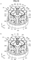
- FIGS. 10 to 12 are diagrams illustrating a manufacturing process of the force sensor device 1.
- the strain generator 20 is made.
- the strain generator 20 can be integrally formed, for example, by molding, cutting, wire discharge, or the like.
- a hard metallic material such as SUS (stainless steel) may be used as the material of the strain generator 20.
- SUS 630 which is particularly hard and of high mechanical strength.
- the strain generator 20 is formed by molding, for example, metal particles and resin as a binder are molded in a metallic mold, and then the resin is sintered to vaporize the resin, thereby forming the strain generator 20 made from metal.
- an adhesive bond 41 is applied to the upper surfaces of the sub-columns 25a-25e and the upper surfaces of the protruding portions 27a-27d.
- an epoxy-based adhesive may be used as the adhesive bond 41. It is preferable that the adhesive bond 41 have a Young's modulus of 1 GPa or more and a thickness of 20 ⁇ m or less from the viewpoint of the resistance to externally applied force.
- a sensor chip 110 is made.
- the sensor chip 110 can be made, for example, by well-known methods of preparing an SOI substrate and etching the prepared substrate (e.g., reactive ion etching, etc.).
- an electrode and/or wiring can be made by, for example, forming a metal film, such as aluminum, on the surface of the substrate by a sputtering method or the like, and then patterning the metal film by photolithography.
- the sensor chip 110 is disposed within the strain generator 20 under pressure so that the lower surface of the sensor chip 110 is in contact with the adhesive bond 41 applied to the upper surface of the sub-columns 25a-25e and the upper surfaces of the protruding portions 27a-27d.
- the adhesive bond 41 is then heated to a predetermined temperature to cure. This secures the sensor chip 110 in the strain generator 20.
- the supporting portions 111a-111d of the sensor chip 110 are secured on the sub-columns 25a-25e
- the supporting portion 111e is secured on the sub-column 25e
- the force points 114a-114d are fixed onto the protruding portions 27a-27d, respectively.
- an adhesive bond 42 is applied to the upper surfaces of the columns 22a-22d.
- an epoxy-based adhesive may be used as the adhesive bond 42.
- the adhesive bond 42 is used to fix the input/output board 30 on the strain generator 20. Since no external force is applied to the adhesive bond 42, a general-purpose adhesive bond can be used.
- the input/output board 30, on which the active components 32-35 and passive component 39 are mounted is prepared and disposed on the strain generator 20 so that the lower surface of the input/output board 30 is in contact with the adhesive bond 42 applied to the upper surfaces of the columns 22a-22d. Then, the input/output board 30 is pressed on the side of the strain generator 20 while the adhesive bond 42 is heated to a predetermined temperature to cure. Thus, the input/output board 30 is fixed to the strain generator 20.
- the input/output board 30 is fixed to the strain generator 20 to outwardly expose the sensor chip 110 and the input portions 24a-24d.
- Each electrode 31 of the input/output board 30 is preferably disposed on the columns 22a-22d of the strain generator 20 with the least strain when force is applied to the input portions 24a-24d.
- the input/output board 30 that extends horizontally from the strain generator 20 (excluding the input terminal side) is bent toward each side surface side of the strain generator 20.
- the corresponding portions of the input/output board 30 and the sensor chip 110 are electrically connected to each other by a bonding wire or the like (not illustrated). With this, the force sensor device 1 is completed.
- the force sensor device 1 can be made of only the three components, namely, the sensor chip 110, the strain generator 20, and the input/output board 30, it is easy to assemble and the number of position registering portions can be minimized, so that the deterioration in accuracy caused by the mounting can be suppressed.
- the strain generator 20 since all the connecting points (the upper surfaces of the sub-columns 25a-25e and the upper surfaces of the protruding portions 27a-27d) with the sensor chip 110 are in the flat plane, the positional registration of the sensor chip 110 relative to the strain generator 20 is sufficient to be only one time, and mounting of the sensor chip 110 onto the strain generator 20 is easy.
- FIG. 13 illustrates the arrangement of piezoresistive elements for detecting the Fz direction force of another example of the sensor chip according to this embodiment.
- the sensor chips illustrated in FIGS. 3 and 6 differ in the shapes of the detecting beams 113a, 113d, 113g, and 113j and the detecting beams 113b, 113e, 113h, and 113k, but eight piezoresistive elements related to Fz are provided in a manner similar to the sensor chips illustrated in FIGS. 3 and 6 .
- the piezoresistive elements FzR2 and FzR3 are disposed at a position that is on a side of the supporting portion 111e relative to a line that bisects the detecting beam 113e and is symmetric with respect to a line that bisects the detecting beam 113f in its longitudinal direction in a region close to the detecting beam 113f of the detecting beam 113e.
- the piezoresistive elements FzR1' and FzR4' are disposed at a position that is on the side of the supporting portion 111e relative to a line bisecting the detecting beam 113e in its longitudinal direction and is symmetric with respect to the line bisecting the detecting beam 113f in its longitudinal direction in regions far from the detecting beam 113f of the detecting beam 113e.
- the piezoresistive elements FzR1 and FzR4 are disposed at a position that is on the side of the supporting portion 111e relative to a line bisecting the detecting beam 113k in its longitudinal direction and is symmetric with respect to the line bisecting the detecting beam 1131 in its longitudinal direction in regions far from the detecting beam 1131 of the detecting beam 113k.
- the piezoresistive elements FzR2' and FzR3' are disposed at a position that is on a side of the supporting portion 111e relative to a line that bisects the detecting beam 113k and is symmetric with respect to a line that bisects the detecting beam 1131 in its longitudinal direction in a region close to the detecting beam 1131 of the detecting beam 113k.
- the sensor chip illustrated in FIG. 13 includes a first detecting portion (R1, R2, R3, and R4) having four strain detecting elements capable of detecting force in a first direction being the Fz direction, and a second detecting portion (R1', R2', R3', and R4') having four strain detecting elements capable of detecting force in the first direction and provided at a position symmetric with respect to the first detecting portion.
- the first detecting portion (R1, R2, R3, and R4) and the second detecting portion (R1', R2', R3', and R4') pass through the center of the substrate and are provided at a position symmetric with respect to a line parallel to the Y-axis.
- the first detecting portion (R1, R2, R3, and R4) and the second detecting portion (R1', R2', R3', and R4') are provided at a position rotation-symmetric with respect to the rotation around the Z-axis by 180 degrees.
- an axis separation property can be improved because of the increased number of the piezoresistive elements and the symmetric arrangement of the piezoresistive elements in addition to the increased accuracy of the sensor.
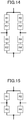
- FIG. 14 illustrates a bridge circuit by a piezoresistive element that detects force in the Fz or Mz direction of the sensor chip according to the embodiment.
- the bridge circuit is formed from a first resistance portion formed by connecting R1 and R1' in series, a second resistance portion formed by connecting R2 and R2' in series, a third resistance portion formed by connecting R3 and R3' in series, and a fourth resistance portion formed by connecting R4 and R4' in series.
- FIG. 15 illustrates the bridge circuit using the piezoresistive element for detecting force in the Fz or Mz direction of the sensor chip in accordance with a reference example.
- the second detecting portion is not provided, and the bridge circuit is formed only by the first detecting portion (R1, R2, R3, and R4).
- the arrangement of the first detecting portion (R1, R2, R3, and R4) are asymmetric, and the axial separation property is not preferable.
- FIG. 16 illustrates a simulation of another axis component of the reference example in which the Fz output is calculated by using only the first detecting portion (R1, R2, R3, and R4) without using the second detecting portion (R1', R2', R3', and R4') in the sensor chip illustrated in FIG. 13 .
- the force of -10N was applied in the Z-axis direction at three locations, where the X-axis coordinates were -15 mm, 0 mm, and +15 mm, and the Fz output at that time was calculated by using a simulation.
- the Fz output is approximately -10 N, but at the positions where the X-axis coordinate is -15 mm and +15 mm, the Fz output is around-12 N and-8 N, respectively, and when only the first detecting portion (R1, R2, R3, and R4) is used, it was confirmed that axis separation in the Fz direction is insufficient.
- FIG. 17 illustrates a simulation of the other axis component according to the embodiment, in which the Fz output is calculated using the first detecting portion (R1, R2, R3, and R4) and the second detecting portion (R1', R2', R3', and R4') in the sensor chip illustrated in FIG. 13 .
- the force of -10N was applied in the Z-axis direction at three locations, where the X-axis coordinates were -15 mm, 0 mm, and +15 mm, and the Fz output at that time was calculated by simulation.
- the Fz output was approximately -10N at all three locations of which the X-axis coordinates were -15 mm, 0 mm, and +15 mm.
Landscapes
- Physics & Mathematics (AREA)
- General Physics & Mathematics (AREA)
- Force Measurement Appropriate To Specific Purposes (AREA)
- Pressure Sensors (AREA)
- Micromachines (AREA)
Abstract
Description
- The present invention relates to a sensor chip and a force sensor device.
- Conventionally, a force sensor device has been known in which a plurality of strain gauges is applied to a strain generator made from a metal, and a strain caused when an external force is applied is converted into an electric signal, thereby detecting a multi-axis direction force. However, this force sensor device has problems in accuracy and productivity because it is necessary to attach strain gauges one by one manually, and it is difficult to downsize the device due to its structure.
- On the other hand, a force sensor device has been proposed in which a strain gauge is replaced with a MEMS sensor chip for a strain detection to solve a problem of lamination accuracy and to achieve miniaturization (see, for example, PTL 1).
- Japanese Patent No.
4011345 - However, in the above-described conventional MEMS force sensor device using the sensor chip, if the input is a single axis (in the direction along any one of six axes [Fx, Fy, Fz, Mx, My, Mz]), the force sensor can perform a high accuracy.
- However, when the input is a composite input (when the input is a composite input along any two or more of the six axes [Fx, Fy, Fz, Mx, My, Mz]), an error of the force sensor is increased due to an insufficient axial separation property, and the accuracy is reduced. In particular, in the case of the composite input, there are combinations of axes of the composite input that does not satisfy an accuracy target value.
- The present invention has been made in view of the above, and is intended to improve the axial separation property and a sensor accuracy for the composite input of the sensor chip.
- The present sensor chip (110) includes a substrate, first supporting portions (111a, 111b, 111c, 111d), a second supporting portion (111e) around which the first support portions are disposed, the second supporting portion being disposed at a center of the substrate, first detecting beams (113a, 113d, 113g, 113j) each connecting the first supporting portions, which are mutually adjacent, second detecting beams (113b, 113e, 113h, 113k) disposed in parallel with the first detecting beams between the first detecting beams and the second supporting portion, force points (114a, 114b, 114c, 114d) disposed in the first detecting beams so as to be applied with force, and a plurality of strain detecting elements disposed a predetermined positions of the first detecting beams and the second detecting beams, wherein the plurality of strain detecting elements includes a first detecting portion having a strain detecting element capable of detecting force in a first direction, and a second detecting portion having a strain detecting element disposed at a position symmetric relative to the first detecting portion.
- The reference numerals in parentheses are appended for ease of understanding and are merely an example and are not limited to the illustrated embodiment.
- The disclosed technique can improve an axial separation property and a sensor accuracy for a composite input of a sensor chip.
-
- [
FIG. 1] FIG. 1 is a perspective view illustrating an example of a force sensor device according to an embodiment. - [
FIG. 2] FIG. 2 is a perspective view illustrating an example of a sensor chip and a strain generator of a force sensor device according to the embodiment. - [
FIG. 3] FIG. 3 is a view illustrating from the upper side in the Z-axis direction of an example of the sensor chip according to the embodiment. - [
FIG. 4] FIG. 4 is a view illustrating from the lower side of the Z-axis direction of an example of the sensor chip according to the embodiment. - [
FIG. 5] FIG. 5 explains reference symbols indicating force and moment applied to each axis according to the embodiment. - [
FIG. 6] FIG. 6 illustrates the arrangement of piezoresistive elements of an example of the sensor chip according to the embodiment. - [
FIG. 7] FIG. 7 is a diagram (1) illustrating an example of the strain generator according to the embodiment. - [
FIG. 8] FIG. 8 is a diagram (2) illustrating an example of the strain generator according to the embodiment. - [
FIG. 9] FIG. 9 is a diagram (3) illustrating an example of the strain generator according to the embodiment. - [
FIG. 10] FIG. 10 is a diagram (1) illustrating an example of a manufacturing process of the force sensor device according to the embodiment. - [
FIG. 11] FIG. 11 is a diagram (2) illustrating an example of the manufacturing process of the force sensor device according to the embodiment. - [
FIG. 12] FIG. 12 is a diagram (3) illustrating an example of the manufacturing process of the force sensor device according to the embodiment. - [
FIG. 13] FIG. 13 illustrates an arrangement of piezoresistive elements for detecting force in the Fz direction of another example of the sensor chip according to the embodiment. - [
FIG. 14] FIG. 14 illustrates a bridge circuit formed by piezoresistive elements that detect force in Fz or Mz direction of the sensor chip according to the embodiment. - [
FIG. 15] FIG. 15 is a diagram illustrating a bridge circuit formed by the piezoresistive elements that detect force in the Fz direction of the sensor chip according to a reference example. - [
FIG. 16] FIG. 16 is a graph explaining a simulation of another axis component for the structure of a reference example. - [
FIG. 17] FIG. 17 is a graph explaining a simulation of another axis component for the structure of the embodiment. - Hereinafter, an embodiment for carrying out the invention with reference to the drawings will be described. In each drawing, the same components are indicated by the same reference numerals and overlapping descriptions may be omitted.
-
FIG. 1 is perspective views illustrating a force sensor device according to a first embodiment.FIG. 2 is a perspective view illustrating a sensor chip and a strain generator of a force sensor device according to a first embodiment. Referring toFIGS. 1 and2 , theforce sensor device 1 includes asensor chip 110, astrain generator 20, and an input/output board 30. Theforce sensor device 1 is, for example, a multi-axis force sensor device mounted on an arm or a finger of a robot used for a machine tool or the like. - The
sensor chip 110 has function of detecting a displacement along predetermined axial directions of up to six axes. Thestrain generator 20 has the function of transferring applied force to thesensor chip 110. - The
sensor chip 110 is bonded to the upper surface side of thestrain generator 20 so as not to protrude from thestrain generator 20. Also, one end side of the input/output board 30 for providing an input/output signals to and from thesensor chip 110 is appropriately bent on the upper surface and each side of thestrain generator 20. Eachelectrode 31 of thesensor chip 110 and the input/output board 30 is electrically connected by a bonding wire (not illustrated) or the like. - In the input/
output board 30, anactive component 32 and apassive component 39 are mounted in a region disposed on the first side of thestrain generator 20. - In the input/
output board 30, anactive component 33 and apassive component 39 are mounted in a region disposed on the second side of thestrain generator 20. In the input/output board 30, anactive component 34 and thepassive component 39 are mounted in a region disposed on the third side of thestrain generator 20. In the input/output board 30, theactive component 35 and thepassive component 39 are mounted in a region disposed on the fourth side of thestrain generator 20. Theactive component 33 is, for example, an IC (AD converter) that converts an analog electric signal from a bridge circuit that detects an X-axis direction force Fx output from thesensor chip 110 and an analog electric signal from a bridge circuit that detects a Y-axis direction force Fy output from thesensor chip 110 into a digital electric signal. - The
active component 34 is, for example, an IC (AD converter) that converts an analog electric signal from a bridge circuit that detects a Z-axis direction force Fz output from thesensor chip 110 and an analog electric signal from a bridge circuit that detects a moment Mx that rotates around the X-axis output from thesensor chip 110 as an axis to a digital electric signal. - The
active component 35 is, for example, an IC (AD converter) that converts an analog electric signal from a bridge circuit that detects a moment My that rotates around the Y-axis as an axis output from thesensor chip 110 and an analog electric signal from a bridge circuit that detects a moment Mz that rotates around the Z-axis as an axis output from thesensor chip 110 into a digital electric signal. - The
active component 32 is, for example, an IC that performs predetermined calculation on digital electric signals output fromactive components passive component 39 may be a resistor, capacitor, or the like, connected to the active components 32-35. - Incidentally, it is optionally possible to determine how many ICs the functions of the
active components 32 to 35 are implemented. Theactive components 32 to 35 may be mounted on the external circuit side connected to the input/output board 30 without mounting theactive components 32 to 35 on the input/output board 30. In this case, an analog electric signal is output from the input/output board 30. - The input/
output board 30 is bent to direct an outside below the first side surface of thestrain generator 20 and the other end of the input/output board 30 is drawn outwardly. On the other end side of the input/output board 30, a terminal (not illustrated) capable of electrical input/output with an external circuit (such as a control device) connected to theforce sensor device 1 is arranged. - In this embodiment, for convenience, in the
force sensor device 1, the side on which thesensor chip 110 is provided is an upper side or one side, and the opposite side is a lower side or the other side. The side of each portion of thesensor chip 110 has one or a upper surface, and the other side has the other side or a bottom surface. However, theforce sensor device 1 may be used in an inverted state or may be disposed at any angle. A plan view refers to viewing an object from the normal direction (Z-axis direction) of the upper surface of thesensor chip 110, and planar shape refers to viewing an object from the normal direction (Z-axis direction) of the upper surface of thesensor chip 110. -
FIG. 3 illustrates thesensor chip 110 viewed from the upper side in the Z-axis direction, in which (a) is a perspective view and (b) is a plan view.FIG. 4 illustrates thesensor chip 110 viewed from the lower side in the Z-axis direction, in which (a) is a perspective view and (b) is a bottom view. In (b) ofFIG. 4 , for convenience, surfaces of the same height are indicated by the same texture. The direction parallel to one side of the upper surface of thesensor chip 110 is the X-axis direction, the direction perpendicular to the one side is the Y-axis direction, and the thickness direction (the normal direction of the upper surface of the sensor chip 110) of thesensor chip 110 is the Z-axis direction. The X-axis direction, the Y-axis direction, and the Z-axis direction are orthogonal to one another. - The
sensor chip 110 illustrated inFIGS. 3 and4 is a MEMS (Micro Electro Mechanical Systems) sensor chip capable of detecting up to six axes in one chip and is formed from a semiconductor substrate such as a SOI (Silicon On Insulator) substrate. The planar shape of thesensor chip 110 may be, for example, a square of about 3000 µm square. - The
sensor chip 110 includes fivecolumnar supporting portions 111a-111e. The planar shape of the supportingportions 111a-111e may be, for example, a square of about 500 µm. The first supportingportions 111a-111d are disposed at four corners of thesensor chip 110. The supportingportion 111e, which is a second supporting portion, is disposed at the center of the supportingportions 111a-111d. - The
support portions 111a-111e may be formed, for example, of an active layer, a BOX layer, and a supporting layer of an SOI substrate, each thickness being, for example, about 500 µm. - Between the supporting
portion 111a and the supportingportion 111b, a reinforcingbeam 112a is provided to reinforce the structure of the supportingportion 111a and the supportingportion 111b fixed at both ends (connecting adjacent supporting portions). Between the supportingportion 111b and the supportingportion 111c, a reinforcingbeam 112b is provided for reinforcing the structure of the supportingportion 111b and the supportingportion 111c (connecting adjacent supporting portions). - Between the supporting
portion 111c and the supportingportion 111d, a reinforcingbeam 112c is provided for reinforcing the structure (connecting adjacent supporting portions) fixed at both ends to the supportingportion 111c and the supportingportion 111d. Between the supportingportion 111d and the supportingportion 111a, a reinforcingbeam 112d is provided for reinforcing the structure of the supportingportion 111d and the supportingportion 111a (connecting adjacent supports to each other). - In other words, the four reinforcing
beam portions - The inner corner of the supporting
portion 111a and the corner of the supportingportion 111e facing thereto are connected by a reinforcingbeam 112e for reinforcing the structure. The inner corner of the supportingportion 111b and the corner of the supportingportion 111e facing thereto are connected by a reinforcingbeam 112f for reinforcing the structure. - The inner corner of the supporting
portion 111c and the corner of the supportingportion 111e facing thereto are connected by a reinforcingbeam 112g for reinforcing the structure. The inner corner of the supportingportion 111d and the corner of the supportingportion 111e facing thereto are connected by a reinforcingbeam 112h for reinforcing the structure. The second reinforcing beam, i.e., the reinforcingbeam 112e-112h, is disposed diagonally with respect to the X-axis direction (the Y-axis direction). That is, the reinforcingbeams 112e-112h are disposed non-parallel to the reinforcingbeams - The reinforcing
beams 112a-112h can be formed, for example, from an active layer, a BOX layer, and a support layer each of an SOI substrate. The thickness (the width in the short-end direction width) of reinforcingbeam 112a-112h may be, for example, about 140 µm. The upper surface of each of the reinforcingbeam 112a-112h is arranged on the same plane as that of the upper surface of the supportingportion 111a-111e. - In contrast, the lower surfaces respectively of the reinforcing
beams 112a-112h are recessed toward the upper surface side by several tens of micrometers from the lower surface of the supportingportions 111a-111e and the lower surfaces of theforce points 114a-114d. This is to prevent the lower surfaces of the reinforcingbeams 112a-112h from contacting the surface of thestrain generator 20 when thesensor chip 110 is bonded to thestrain generator 20. - In this manner, the rigidity of the
sensor chip 110 in its entirety can be made high by disposing the reinforcing beam, which is formed to be thicker than the detecting beam for detecting distortion, in addition to the detecting beam. As a result, because it is difficult to deform other than the detecting beam in response to an input, good sensor characteristics can be obtained. - Inside the reinforcing
beam 112a between the supportingportion 111a and the supportingportion 111b, the detectingbeam 113a for detecting the distortion is provided for detecting distortion, both ends of which are fixed to the supportingportion 111a and the supportingportion 111b at predetermined intervals in parallel with the reinforcingbeam 112a (connecting adjacent supporting portions to each other) . - Between the detecting
beam 113a and the supportingportion 111e, the detectingbeam 113b is provided in parallel with the detectingbeam 113a interposing a predetermined interval with the detectingbeam 113a and the supportingportion 111e. The detectingbeam 113b connects an end of the reinforcingbeam 112e on the side of the supportingportion 111e with an end of the reinforcingbeam 112f on the side of the supportingportion 111e. - The generally central longitudinal portion of the detecting
beam 113a and the longitudinally central portion of the opposing detectingbeam 113b are coupled by a detectingbeam 113c positioned perpendicular to the detectingbeam 113a and the detectingbeam 113b. - Inside the reinforcing
beam 112b between the supportingportion 111b and the supportingportion 111c, a detectingbeam 113d is disposed for detecting distortion (mutually connecting adjacent supporting portions). Both ends of the detectingbeam 113d are respectively fixed to the supportingportion 111b and the supportingportion 111c in parallel with the reinforcingbeam 112b while interposing a predetermined interval. - Between the detecting
beam 113d and the supportingportion 111e, a detectingbeam 113e is disposed in parallel with the detectingbeam 113d while interposing a predetermined interval between the detectingbeam 113d and the supportingportion 111e. The detectingbeam 113e connects an end of the reinforcingbeam 112f on the side of the supportingportion 111e with an end of the reinforcingbeam 112g on the side of the supportingportion 111e. - A substantially central portion in the longitudinal direction of the detecting
beam 113d and a substantially central portion in the longitudinal direction of the detectingbeam 113e facing the detectingbeam 113d are connected by a detectingbeam 113f disposed in perpendicular to the detectingbeam 113d and the detectingbeam 113e. - Inside the reinforcing
beam 112c between the supportingportion 111c and the supportingportion 111d, a detectingbeam 113g is disposed for detecting distortion, wherein both ends of the detectingbeam 113g are fixed to the supportingportion 111c and the supportingportion 111d in parallel with the reinforcingbeam 112c while interposing a predetermined interval between the detectingbeam 113g and the reinforcingbeam 112c (adjacent supporting portions are connected to each other). - Between the detecting
beam 113g and the supportingportion 111e, the detectingbeam 113h is disposed in parallel with the detectingbeam 113g while interposing a predetermined interval between the detectingbeam 113h and the detectingbeam 113g. The detectingbeam 113h connects an end of the reinforcingbeam 112g on the side of the supportingportion 111e with an end of the reinforcingbeam 112h on the side of the supportingportion 111e. - A substantially central portion in the longitudinal direction of the detecting
beam 113g and a substantially central portion in the longitudinal direction of the detectingbeam 113h facing the detectingbeam 113g are connected by a detectingbeam 113i disposed in perpendicular to the detectingbeam 113g and the detectingbeam 113h. - Inside the reinforcing
beam 112d between the supportingportion 111d and the supportingportion 111a, a detectingbeam 113j is disposed for detecting distortion, wherein both ends of the detectingbeam 113j are fixed to the supportingportion 111d and the supportingportion 111a in parallel with the reinforcingbeam 112d while interposing a predetermined interval between the detectingbeam 113j and the reinforcingbeam 112d (adjacent supporting portions are connected to each other). - Between the detecting
beam 113j and the supportingportion 111e, the detectingbeam 113k is disposed in parallel with the detectingbeam 113j while interposing a predetermined interval between the detectingbeam 113h and the detectingbeam 113g. The detectingbeam 113k connects an end of the reinforcingbeam 112h on the side of the supportingportion 111e with an end of the reinforcingbeam 112e on the side of the supportingportion 111e. - A substantially central portion in the longitudinal direction of the detecting
beam 113j and a substantially central portion in the longitudinal direction of the detectingbeam 113k facing the detectingbeam 113i are connected by a detectingbeam 1131 disposed in perpendicular to the detectingbeam 113j and the detectingbeam 113k. - The detecting
beams 113a-113l are disposed on the upper end side in the thickness direction of the supportingportions 111a-111e and can be formed, for example, from the active layer of the SOI substrate. The width (connecting beam) of the detectingbeams 113a-113l may be, for example, about 75 µm. The width (short-end direction) of the detectingbeams 113a-1131 may vary depending on the position. The upper surface of each of the detectingbeams 113a-113l is substantially on the same plane as that of the upper surface of the supportingportions 111a-111e. The thickness of each of the detectingbeams 113a-113l may be, for example, about 50 µm. - A
force point 114a is provided on the lower surface side (an intersection point between the detectingbeam 113a and the detectingbeam 113c) of the central portion of the detectingbeam 113a in the longitudinal direction. The detectingbeams force points 114a. - A
force point 114b is provided on the lower surface of the central portion of the detectingbeam 113d in the longitudinal direction (an intersection point between the detectingbeam 113d and the detectingbeam 113f). The detectingbeams force point 114b form a set of detecting blocks. - A
force point 114c is provided on the lower surface of the central portion of the detectingbeam 113g in the longitudinal direction (an intersection of the detectingbeam 113g and the detectingbeam 113i). The detectingbeams force point 114c form a set of detecting blocks. - A
force point 114d is provided on the lower surface (an intersection point between the detectingbeam 113j and the detecting beam 1131) of the central portion of the detectingbeam 113j in the longitudinal direction. A set of detecting blocks is formed by the detectingbeams force point 114d. - At the
force points 114a-114d, external force is applied and can be formed, for example, from the BOX layer and the supporting layer of the SOI substrate. The lower surface of each of theforce points 114a-114d is roughly flush with the bottom surface of thesupport portions 111a-111e. - Thus, by taking in the force or displacement from the four
force points 114a to 114d, the deformation of the beams differs for each type of force, so that a sensor with a good 6-axis separation property can be implemented. - In the
sensor chip 110, from the viewpoint of suppressing stress concentration, it is preferable that a portion forming the inner angle be in a R-like shape. -
FIG. 5 illustrates a reference symbol indicating force and a moment applied to each axis. As illustrated inFIG. 5 , the X-axis direction force is Fx, the Y-axis direction force is Fy, and the Z-axis direction force is Fz. The moment to rotate around the X axis is Mx, the moment to rotate around the Y axis is My, and the moment to rotate around the Z axis as the axis is Mz. -
FIG. 6 illustrates the arrangement of piezoresistive elements of thesensor chip 110. A plurality of strain detecting elements, a piezoresistive element, is disposed in a predetermined position of each detecting block corresponding to fourforce points 114a to 114d. - Specifically, referring to
FIGS. 3 and6 , in the detecting block corresponding to theforce point 114a, the piezoresistive elements MxR3 and MxR4 are disposed at the position symmetric with respect to a line that bisects the detectingbeam 113a in the longitudinal direction and are symmetric with respect to a line that bisects the detectingbeam 113c in the longitudinal direction (the Y direction) in a region close to the detectingbeam 113c. The piezoresistive elements FyR3 and FyR4 are positioned on the side of the reinforcingbeam 112a relative to the line dividing the detectingbeam 113a in the longitudinal direction equally, and at the position symmetric relative to the line dividing the detectingbeam 113c in the longitudinal direction at a distance from the detectingbeam 113c. The piezoresistive elements MzR3' and MzR4' are disposed on a line that bisects the detectingbeam 113a in the longitudinal direction and at the position symmetric relative to a line that bisects the detectingbeam 113c in the longitudinal direction in a region near the midpoint of the connection between thesupport portion 111a and theend portion 111b of the detectingbeam 113a and the detectingbeam 113c. - In the detecting block corresponding to the
force point 114b, the piezoresistive elements MyR3 and MyR4 are arranged on a line that bisects the detectingbeam 113d in the longitudinal direction and at the position symmetric relative to a line that bisects the detectingbeam 113f in the longitudinal direction (the X direction) in a region near the detectingbeam 113f of the detectingbeam 113d. The piezoresistive elements FxR3 and FxR4 are disposed at a position symmetric to a line that is more than a line that divides the detectingbeam 113d equally in the longitudinal direction and a line that divides the detectingbeam 113f in the longitudinal direction in a region far from the detectingbeam 113f of the detectingbeam 113d. The piezoresistive elements MzR3 and MzR4 are disposed on a line that bisects the detectingbeam 113d in the longitudinal direction and at the position symmetric with respect to a line that bisects the detectingbeam 113f in the longitudinal direction in a region near the midpoint of the connecting portion between the end on a side of the supportingportions beam 113d and the detectingbeam 113f. - The piezoresistive elements FzR2 and FzR3 are disposed on a line that bisects the detecting
beam 113e in the longitudinal direction and at the position symmetric relative to a line that bisects thebeam 113f longitudinal direction in a region close to the detectingbeam 113f of the detectingbeam 113e. The piezoresistive elements FzR1' and FzR4' are arranged on a line that bisects the detectingbeam 113e in the longitudinal direction and at the position symmetric relative to a line that bisects the detectingbeam 113f in the longitudinal direction in a distance from the detectingbeam 113f of the detectingbeam 113e. - In the detecting block corresponding to the
force point 114c, the piezoresistive elements MxR1 and MxR2 are disposed on a line that bisects the detectingbeam 113g in the longitudinal direction and at the position symmetric relative to a line that bisects the detectingbeam 113i in the longitudinal direction (the Y direction) in a region close to the detectingbeam 113i. The piezoresistive elements FyR1 and FyR2 are disposed on the side of the reinforcingbeam 112c relative to the line that bisects the detectingbeam 113g in the longitudinal direction equally, and at the position symmetric relative to the line that bisects the detectingbeam 113i in the longitudinal direction in a distance from the detectingbeam 113i. The piezoresistive elements MzR1' and MZR2' are disposed on a line that bisects the detectingbeam 113g in the longitudinal direction and at a position symmetric relative to a line that bisects the detectingbeam 113i in the longitudinal direction in a region near the midpoint of the connecting portion between the end of the detectingbeam 113g on the side of the supportingportions beam 113i. - In the detecting block corresponding to the
force point 114d, the piezoresistive elements MyR1 and MyR2 are arranged on a line that bisects the detectingbeam 113j in the longitudinal direction and at the position symmetric relative to a line that bisects the detectingbeam 1131 in the longitudinal direction (X direction) in a region close to the detectingbeam 1131 of the detecting beam113j. The piezoresistive elements FxR1 and FxR2 are disposed at a position symmetric to a line that is more distal to the reinforcingbeam 112d than the line that bisects the detectingbeam 113j in the longitudinal direction and bisects the detectingbeam 1131 in the longitudinal direction in a region far from the detectingbeam 1131 of the detectingbeam 113j. The piezoresistive elements MzR1 and MzR2 are disposed on a line that bisects the detectingbeam 113j in the longitudinal direction and at the position symmetric relative to a line that bisects the detectingbeam 1131 in the longitudinal direction in a region near the midpoint of the connecting portion between the end on the side of thesupport portions beam 113j and the detectingbeam 1131. - The piezoresistive elements FzR1 and FzR4 are disposed on a line that bisects the detecting
beam 113k in the longitudinal direction and at a position symmetric relative to a line that bisects the detectingbeam 1131 in the longitudinal direction in a region far from the detectingbeam 1131 of the detectingbeam 113k. The piezoresistive elements FzR2' and FzR3' are arranged on a line that bisects the detectingbeam 113k in the longitudinal direction and at the position symmetric relative to a line that bisects the detectingbeam 1131 in the longitudinal direction in a region close to the detectingbeam 1131 of the detectingbeam 113k. - In this manner, a plurality of piezoresistive elements are disposed separately in each detecting block of the
sensor chip 110.
This allows a predetermined axial displacement of up to six axes to be detected based on a change in the output of a plurality of piezoresistive elements disposed in a predetermined beam according to the direction (axial direction) of the force applied (transmitted) to theforce points 114a-114d. - The
sensor chip 110 has a structure such that the detectingbeams beams beams beams beams - In the
sensor chip 110, a piezoresistive element is not disposed in the detectingbeams beams beams beams sensor chip 110 can efficiently capture stress so as to improve sensitivity (the change in resistance of the piezoresistive element to the same stress). - In the
sensor chip 110, a dummy piezoresistive element is disposed in addition to the piezoresistive element used for detecting distortion. The dummy piezoresistive element is arranged such that all piezoresistive elements, including the piezoresistive elements used for detecting distortion, are point-symmetric relative to the center of the supportingportion 111e. - Here, the piezoresistive elements FxR1 to FxR4 detect force Fx, piezoresistive elements FyR1 to FyR4 detect force Fy, and piezoresistive elements FzR1 to FzR4, and FzR1' to FzR4' detect force Fz. The piezoresistive elements MxR1-MxR4 detect moment Mx, the piezoresistive elements MyR1-MyR4 detect moment My, and the piezoresistive elements MzR1-MzR4 and MzR1'-MzR4' detect moment Mz.
- In this manner, a plurality of piezoresistive elements are separately disposed in each detecting block in the
sensor chip 110. This allows a displacement in a predetermined axial direction to be detected up to six axes based on a change in the output of a plurality of piezoresistive elements disposed on a predetermined beam in response to the force applied (transmitted) to or a displacement orientation (axial direction) at theforce points 114a-114d. - In the sensor chip according to the above embodiment, a plurality of strain detecting elements of piezoresistive elements include a first detecting portion (R1, R2, R3, R4) having four strain detecting elements capable of detecting force in a first direction in the Fz direction or in the Mz direction, and a second detecting portion (R1', R2', R3', R4') having four strain detecting elements capable of detecting force in the first direction and disposed at a position symmetric relative to the first detecting portion. That is, the moment (Mx, My) in the X-axis direction and Y-axis direction can be detected based on the deformations of the first detecting
beam beams - In the
sensor chip 110, the displacement (Fx, Fy, Mz) in the X-axis direction and the Y-axis direction can be detected based on the deformation of the predetermined detecting beam. That is, the force (Fx, Fy) in the X-axis direction and the Y-axis direction can be detected based on the deformation of the detectingbeams beams - In the sensor chip according to the above embodiment, a plurality of strain detecting elements of piezoresistive elements include a first detecting portion (R1, R2, R3, R4) having four strain detecting elements capable of detecting force in a first direction in the Fz direction or in the Mz direction, and a second detecting portion (R1', R2', R3', R4') having four strain detecting elements capable of detecting force in the first direction and disposed at a position symmetric relative to the first detecting portion. Here, when the first direction is the Fz direction, the first detecting portion is FzR1 to FzR4, and the second detecting portion is FzR1' to FzR4'. For example, FzR2 and FzR3, which are a part of the first detecting portion, and FzR1' and FzR4', which are a part of the second detecting portion, are formed in one second detecting
beam 113e, and the remainder of the first detecting portion, FzR1 and FzR4, which are a part of the second detecting portion, and the remainder of the second detecting portion, FzR2' and FzR3' are formed in another second detectingbeam 113k, which is provided in parallel with the second detectingbeam 113e. Alternatively, when the first direction is the Mz direction, the first detecting portion is MzR1 to MzR4 and the second detecting portion is MzR1' to MzR4'. For example, a first detecting portion MzR1 to MrR4 is formed on a pair of first detectingbeam beam - More specifically, the first direction is the Fz direction, and the first and second detectors pass through the center of the substrate and are disposed at a position line-symmetric with respect to a line parallel to the Y-axis. That is, piezoresistive elements FzR1-FzR4 and piezoresistive elements FzR1'-FzR4' pass through the center of the substrate and are disposed at a position line-symmetric with respect to a line parallel to the Y-axis, as illustrated in
FIGS. 3 and6 . - Alternatively, the first direction is the Fz direction, and the first detecting portion and the second detecting portion are disposed at a position rotation-symmetric with respect to the rotation around the Z-axis by 180 degrees. That is, the piezoresistive elements FzR1-FzR4 and the piezoresistive elements FzR1'-FzR4' are disposed at a position rotation-symmetric by 180 degrees relative to the rotation around the Z-axis, as illustrated in
FIGS. 3 and6 . - Alternatively, the above-described first direction is in the Mz direction, and the first detecting portion and the second detecting portion are disposed at a position rotation-symmetric with respect to the rotation around the Z-axis by 90 degrees. That is, the piezoresistive elements MzR1-MzR4 and the piezoresistive elements MzR1'-MzR4' are disposed at a position rotation-symmetry by 90 degrees with respect to the rotation around the Z-axis, as illustrated in
FIGS. 3 and6 . - In the sensor chip of this embodiment, one bridge circuit is provided for one of the axes to be detected. When the above-described first direction is the Fz direction, the first detecting portion is FzR1 to FzR4, and the second detecting portion is FzR1' to FzR4', the bridge circuit corresponding to Fz is formed from eight piezoresistive elements in total of four piezoresistive elements of the first detecting portion and four piezoresistive elements of the second detecting portion. Specifically, the bridge circuit is formed from the first, second, third, and fourth resistance portions by connecting FzR1 and FzR1' in series to form a first resistance portion, FzR2 and FzR2' in series to form a second resistance portion, FzR3 and FzR3' in series to form a third resistance portion, and FzR4 and FzR4' in series to form a fourth resistance portion.
- In addition, when the above-described first direction is in the Mz direction, the first detecting portion is MzR1 to MzR4, and the second detecting portion is the MzR1' to MzR4', the bridge circuit corresponding to Mz is formed from a total of eight piezoresistive elements including four piezoresistive elements of the first detecting portion and four piezoresistive elements of the second detecting portion. Specifically, the bridge circuit is formed from a first resistance portion, second resistance portion, third resistance portion, and fourth resistance portion, wherein MzR1 and MzR1' are connected in series to form the first resistance portion, MzR2 and the MzR2' are connected in series to form the second resistance portion, MzR3 and MzR3' are connected in series to form the third resistance portion, and MzR4 and MzR4' are connected in series to form the fourth resistance portion.
- It is also possible to include a first detecting portion (R1, R2, R3, and R4) having four strain detecting elements capable of detecting force in the first direction being the Fz direction, a second detecting portion (R1', R2', R3', and R4') having four strain detecting elements capable of detecting force in the first direction having four strain detecting elements provided at a position symmetric relative to the first detecting portion, and a third detecting portion (R1, R2, R3, and R4) having four strain detecting elements capable of detecting force in the second direction being the Mz direction, and a fourth detecting portion (R1', R2', R3', and R4') having four strain detecting elements provided at a position symmetric relative to the third detecting portion.
- According to the sensor chip of this embodiment described above, the number of piezoresistive elements corresponding to Fz or Mz increases and the arrangement is symmetrical. When the piezoresistive element is not disposed symmetrically, a multi-axis interference occurs when a composite input is made to the force sensor device, and an axial separation property is degraded. In this embodiment, the axis separation property can be improved because the number of the piezoresistive elements is increased and the accuracy of the sensor is enhanced, and the placement of the arrangement of the piezoresistive elements is symmetrical.
- For example, the resistance value of the strain detecting element (piezoresistive element) of the first detecting portion and the second detecting portion is half the resistance value of the strain detecting element other than the first detecting portion and the second detecting portion. As described above, a composite resistance in which one piezoresistive element of the first detecting portion and a corresponding one piezoresistive element of the second detecting portion are connected in series can be regarded as one resistive element of a bridge circuit. Accordingly, the resistance value of the piezoresistive elements of the first detecting portion and the second detecting portion may be about half that of other piezoresistive elements. In other words, the number of resistance elements is increased by doubling the number of the resistance elements and halving the resistance value of the piezoresistive element related to the conventional Fz or Mz (by dividing the resistive element), and the increased number of the resistance elements is disposed at a position line-symmetric or rotation-symmetric relative to the existing resistive element.
- By varying the thickness and width of each detecting beam, it is possible to equalize the detection sensitivity and improve the detection sensitivity.
- However, it is also possible to reduce the number of piezoresistive elements and provide a sensor chip for detecting predetermined axial displacements of 5 or less axes.
- According to the sensor chip of the present embodiment described above, by disposing the piezoresistive element so as to be geometrically symmetric according to the shape of the beam, it is possible to accurately detect the six-component force even when the force and moment are input in a composite manner. In addition, when the number of piezoresistive elements is increased to make the symmetric arrangement, the combined resistance applied to the bridge circuit can be controlled simply by changing the size of the piezoresistive elements, so that the resistance value can be easily adjusted and the load on the circuit design is low. In addition, even if the number of the piezoresistive elements is increased, the number of steps does not increase and does not lead to an increase in cost, since the piezoresistive elements can be manufactured by a semiconductor process using a photolithographic process. On the other hand, the strain gauge is applied to the strain generator and it is almost impossible to increase the number of piezoresistive elements and arrange them symmetrically. However, it is possible in the force sensor device of this embodiment using the MEMS-type sensor chip.
-
FIG. 7 is a diagram (first view) illustrating thestrain generator 20, InFIG. 7 , (a) is a perspective view, and (b) is a side view. InFIG. 8 , (a) is a plan view and (b) is a longitudinal perspective view along the A-A line of (a). InFIG. 8 , (a), for convenience, surfaces of the same height are indicated by the same satin pattern.FIG. 9 is a view (third view) illustrating thestrain generator 20. InFIG. 9 , (a) is a vertical cross-sectional view along a B-B line ofFIG. 8 , (a), and (b) is a horizontal cross-sectional view along a C-C line of (a). - As illustrated in
FIGS. 7-9 , thestrain generator 20 includes a base 21 which is mounted directly onto a fixture portion, asupport column 28 which is a sensor chip mounting portion mounting thesensor chip 110, andcolumns 22a-22d disposed around the support column while interposing a space in the periphery of thesupport column 28. - More specifically, in the
strain generator 20, fourcolumns 22a-22d are disposed on the upper surface of the base 21 in a circle-like shape to be even (point-symmetry) relative to the center of thebase 21, and fourbeams 23a-23d, which are the first beams connecting adjacent columns together, are provided so as to be formed like a frame. Then, thesupport column 28 is disposed above the center of the upper surface of thebase 21. The planar shape of thebase 21 is not limited to the shape like circle, but may be a shape like a polygon (e.g., square). - The
support column 28 is formed to be thicker and shorter than thecolumns 22a-22d. Thesensor chip 110 is fixed onto thesupport column 28 so as not to protrude from the upper surfaces of thecolumns 22a-22d. - The
support column 28 is not secured directly to the upper surface of thebase 21, but is secured to thecolumns 22a-22d via connectingbeams 28a-28d. Therefore, there is space between the upper surface of thebase 21 and the lower surface of thesupport column 28. The lower surface of thesupport column 28 and the lower surfaces of each of the connectingbeams 28a-28d may be on a flat surface. - The cross-sectional shape of the portion to which the connecting
beams 28a-28d of thesupport column 28 is connected is in a, for example, a rectangular shape, with the four corners of the rectangular shape and thecolumns 22a-22d facing the four corners of the rectangular shape being connected via the connectingbeams 28a-28d. Preferably, positions 221-224 at which the connectingbeams 28a-28d are connected to thecolumns 22a-22d are below midway in the height direction of thecolumns 22a-22d. The reasons for this are described later. The cross-sectional shape of a part to which the connectingbeams 28a to 28d of thesupport column 28 are connected is not limited to a rectangular shape, but may be a circular shape or a polygonal shape (for example, a hexagon shape). - The connecting
beams 28a-28d are disposed substantially parallel to the upper surface of the base 21 while interposing predetermined intervals between the upper surface of thebase 21 and the connectingbeams 28a-28d so as to be equal (point-symmetry) with respect to the center of thebase 21. The width and thickness (rigidity) of the connectingbeams 28a-28d are preferably narrower and thinner than thecolumns 22a-22d and thebeams 23a-23d so as not to prevent the deformation of thestrain generator 20. - Thus, the upper surface of the
base 21 and the lower surface of thesupport column 28 are separated by a predetermined distance. The predetermined distance may be, for example, on the order of several millimeters. - In the
base 21, a throughhole 21x is provided for fastening thestrain generator 20 to the fixture portion using a screw or the like. In this embodiment, thebase 21 is provided with four through-holes 21x, but the number of through-holes 21x can be arbitrarily determined. - Except for the
base 21, thestrain generator 20 may have a rectangular shape, for example, about 5000 µm in length, about 5000 µm in width, and about 7000 µm in height. The cross-sectional shape of thecolumns 22a-22d may be, for example, square of about 1000µm square. The cross-sectional shape of thepost 28 may be, for example, a square of about 2000 µm square. - However, from the viewpoint of suppressing stress concentration in the
strain generator 20, it is preferable that the portion forming the inner angle be in a shape like R. For example, the central surface of the upper surface of thepedestal 21 of thecolumns 22a-22d is preferably formed in an R-shape. Similarly, surfaces facing the upper surface of thebase 21 ofbeams 23a-23d are preferably formed in the R-shape on the right and left sides. - A central portion in the longitudinal direction of each of the upper surfaces of the
beams 23a-23d is provided with a protruding portion upwardly protruding from the central portion of thebeams 23a-23d in the longitudinal direction, andinput portions 24a-24d in a shape like quadrangular prism are provided on the protruding portion. Theinput portions 24a-24d are externally applied with force, and when the force is applied to inputportions 24a-24d, thebeams 23a-23d and thecolumns 22a-22d are deformed accordingly. - Thus, by providing four
input portions 24a-24d, the load resistance of thebeams 23a-23d can be improved in comparison with, for example, the structure of one input portion. - Four
sub-columns 25a-25d are disposed in the four corners of the upper surface of thesupport column 28, and afourth pillar 25e is disposed in the center of the upper surface of thesupport column 28. The sub-columns 25a-25e are formed so as to have the same height. - That is, the upper surfaces of each of the sub-columns 25a-25e are on the same flat plane. Each upper surface of the sub-columns 25a-25e is a junction bonded to the lower surface of the
sensor chip 110. - Central portions of inner side surfaces of the
beams 23a-23d are provided with sub-beams 26a-26d projecting horizontally inwardly from each of the inner surfaces of thebeams 23a-23d. The sub-beams 26a-26d are second beams that transmit deformation of thebeams 23a-23d andcolumns 22a-22d tosensor chip 110. Front end side of the upper surfaces of the sub-beams 26a-26d are also provided with protrudingportions 27a-27d projecting upwardly from the front end side of the upper surfaces of the sub-beams 26a-26d, respectively. - The protruding
portions 27a-27d are formed to have the same height. That is, the upper surfaces of the protrudingportions 27a-27d are on the same flat plane. Each upper surface of the protrudingportions 27a-27d is a joining portion bonded to the lower surface of thesensor chip 110. The sub-beams 26a-26d and protrudingportions 27a-27d are connected to thebeams 23a-23d as movable portions. Therefore, these are deformed when force is applied to theinput portions 24a-24d. - Incidentally, in a state where no force is applied to the
input portions 24a to 24d, the respective upper surfaces of the sub-columns 25a-25e and the respective upper surfaces of the protrudedportions 27a to 27d are positioned on the same plane. - The portions of the
base 21,columns 22a-22d,support column 28,beams 23a-23d,input portions 24a-24d, sub-columns 25a-25e, sub-beams 26a-26d, and protrudingportions 27a-27d are preferably integrally formed from a viewpoint of ensuring rigidity and precisely manufacturing. For example, a hard metallic material such as SUS (stainless steel) may be used as the material of thestrain generator 20. Among them, it is preferable to use SUS 630 which is particularly rigid and of high mechanical strength. - Thus, as with the
sensor chip 110, thestrain generator 20 is also constructed with columns and beams, so that the deformation of each of the six axes is caused by the applied force, so that the deformation of the six axes with good separation can be transmitted to thesensor chip 110. - That is, the force applied to the
input portions 24a-24d of thestrain generator 20 is transmitted to thesensor chip 110 viacolumns 22a-22d, thebeams 23a-23d, and the sub-beams 26a-26d, and the displacement is detected by thesensor chip 110. Then, in thesensor chip 110, the output of each axis can be obtained from a bridge circuit formed one by one for each axis. -
FIGS. 10 to 12 are diagrams illustrating a manufacturing process of theforce sensor device 1. First, as illustrated in (a) ofFIG. 10 , thestrain generator 20 is made. Thestrain generator 20 can be integrally formed, for example, by molding, cutting, wire discharge, or the like. For example, a hard metallic material such as SUS (stainless steel) may be used as the material of thestrain generator 20. Among them, it is preferable to use a SUS 630 which is particularly hard and of high mechanical strength. When thestrain generator 20 is formed by molding, for example, metal particles and resin as a binder are molded in a metallic mold, and then the resin is sintered to vaporize the resin, thereby forming thestrain generator 20 made from metal. - Next, in the process illustrated in (b) of
FIG. 10 anadhesive bond 41 is applied to the upper surfaces of the sub-columns 25a-25e and the upper surfaces of the protrudingportions 27a-27d. For example, an epoxy-based adhesive may be used as theadhesive bond 41. It is preferable that theadhesive bond 41 have a Young's modulus of 1 GPa or more and a thickness of 20 µm or less from the viewpoint of the resistance to externally applied force. - Next, in the step illustrated in (a) of
FIG. 11 , asensor chip 110 is made. Thesensor chip 110 can be made, for example, by well-known methods of preparing an SOI substrate and etching the prepared substrate (e.g., reactive ion etching, etc.). Further, an electrode and/or wiring can be made by, for example, forming a metal film, such as aluminum, on the surface of the substrate by a sputtering method or the like, and then patterning the metal film by photolithography. - Next, in the process illustrated in (b) of
FIG. 11 , thesensor chip 110 is disposed within thestrain generator 20 under pressure so that the lower surface of thesensor chip 110 is in contact with theadhesive bond 41 applied to the upper surface of the sub-columns 25a-25e and the upper surfaces of the protrudingportions 27a-27d. Theadhesive bond 41 is then heated to a predetermined temperature to cure. This secures thesensor chip 110 in thestrain generator 20. Specifically, the supportingportions 111a-111d of thesensor chip 110 are secured on the sub-columns 25a-25e, the supportingportion 111e is secured on thesub-column 25e, and theforce points 114a-114d are fixed onto the protrudingportions 27a-27d, respectively. - Next, in the process illustrated in (a) of
FIG. 12 , anadhesive bond 42 is applied to the upper surfaces of thecolumns 22a-22d. For example, an epoxy-based adhesive may be used as theadhesive bond 42. Theadhesive bond 42 is used to fix the input/output board 30 on thestrain generator 20. Since no external force is applied to theadhesive bond 42, a general-purpose adhesive bond can be used. - Next, in the process illustrated in (b) of
FIG. 12 , the input/output board 30, on which the active components 32-35 andpassive component 39 are mounted, is prepared and disposed on thestrain generator 20 so that the lower surface of the input/output board 30 is in contact with theadhesive bond 42 applied to the upper surfaces of thecolumns 22a-22d. Then, the input/output board 30 is pressed on the side of thestrain generator 20 while theadhesive bond 42 is heated to a predetermined temperature to cure. Thus, the input/output board 30 is fixed to thestrain generator 20. - The input/
output board 30 is fixed to thestrain generator 20 to outwardly expose thesensor chip 110 and theinput portions 24a-24d. Eachelectrode 31 of the input/output board 30 is preferably disposed on thecolumns 22a-22d of thestrain generator 20 with the least strain when force is applied to theinput portions 24a-24d. - Thereafter, a portion of the input/
output board 30 that extends horizontally from the strain generator 20 (excluding the input terminal side) is bent toward each side surface side of thestrain generator 20. The corresponding portions of the input/output board 30 and thesensor chip 110 are electrically connected to each other by a bonding wire or the like (not illustrated). With this, theforce sensor device 1 is completed. - As described above, since the
force sensor device 1 can be made of only the three components, namely, thesensor chip 110, thestrain generator 20, and the input/output board 30, it is easy to assemble and the number of position registering portions can be minimized, so that the deterioration in accuracy caused by the mounting can be suppressed. - In addition, in the
strain generator 20, since all the connecting points (the upper surfaces of the sub-columns 25a-25e and the upper surfaces of the protrudingportions 27a-27d) with thesensor chip 110 are in the flat plane, the positional registration of thesensor chip 110 relative to thestrain generator 20 is sufficient to be only one time, and mounting of thesensor chip 110 onto thestrain generator 20 is easy. -
FIG. 13 illustrates the arrangement of piezoresistive elements for detecting the Fz direction force of another example of the sensor chip according to this embodiment. The sensor chips illustrated inFIGS. 3 and6 differ in the shapes of the detectingbeams beams FIGS. 3 and6 . - In the sensor chip of
FIG. 13 , the piezoresistive elements FzR2 and FzR3 are disposed at a position that is on a side of the supportingportion 111e relative to a line that bisects the detectingbeam 113e and is symmetric with respect to a line that bisects the detectingbeam 113f in its longitudinal direction in a region close to the detectingbeam 113f of the detectingbeam 113e. The piezoresistive elements FzR1' and FzR4' are disposed at a position that is on the side of the supportingportion 111e relative to a line bisecting the detectingbeam 113e in its longitudinal direction and is symmetric with respect to the line bisecting the detectingbeam 113f in its longitudinal direction in regions far from the detectingbeam 113f of the detectingbeam 113e. The piezoresistive elements FzR1 and FzR4 are disposed at a position that is on the side of the supportingportion 111e relative to a line bisecting the detectingbeam 113k in its longitudinal direction and is symmetric with respect to the line bisecting the detectingbeam 1131 in its longitudinal direction in regions far from the detectingbeam 1131 of the detectingbeam 113k. The piezoresistive elements FzR2' and FzR3' are disposed at a position that is on a side of the supportingportion 111e relative to a line that bisects the detectingbeam 113k and is symmetric with respect to a line that bisects the detectingbeam 1131 in its longitudinal direction in a region close to the detectingbeam 1131 of the detectingbeam 113k. - The sensor chip illustrated in
FIG. 13 includes a first detecting portion (R1, R2, R3, and R4) having four strain detecting elements capable of detecting force in a first direction being the Fz direction, and a second detecting portion (R1', R2', R3', and R4') having four strain detecting elements capable of detecting force in the first direction and provided at a position symmetric with respect to the first detecting portion. For example, the first detecting portion (R1, R2, R3, and R4) and the second detecting portion (R1', R2', R3', and R4') pass through the center of the substrate and are provided at a position symmetric with respect to a line parallel to the Y-axis. Alternatively, the first detecting portion (R1, R2, R3, and R4) and the second detecting portion (R1', R2', R3', and R4') are provided at a position rotation-symmetric with respect to the rotation around the Z-axis by 180 degrees. - In the sensor chip described above, an axis separation property can be improved because of the increased number of the piezoresistive elements and the symmetric arrangement of the piezoresistive elements in addition to the increased accuracy of the sensor.
-
FIG. 14 illustrates a bridge circuit by a piezoresistive element that detects force in the Fz or Mz direction of the sensor chip according to the embodiment. When the first detecting portion (R1, R2, R3, R4) and the second detecting portion (R1', R2', R3', R4') are provided, the bridge circuit is formed from a first resistance portion formed by connecting R1 and R1' in series, a second resistance portion formed by connecting R2 and R2' in series, a third resistance portion formed by connecting R3 and R3' in series, and a fourth resistance portion formed by connecting R4 and R4' in series. -
FIG. 15 illustrates the bridge circuit using the piezoresistive element for detecting force in the Fz or Mz direction of the sensor chip in accordance with a reference example. The second detecting portion is not provided, and the bridge circuit is formed only by the first detecting portion (R1, R2, R3, and R4). The arrangement of the first detecting portion (R1, R2, R3, and R4) are asymmetric, and the axial separation property is not preferable. -
FIG. 16 illustrates a simulation of another axis component of the reference example in which the Fz output is calculated by using only the first detecting portion (R1, R2, R3, and R4) without using the second detecting portion (R1', R2', R3', and R4') in the sensor chip illustrated inFIG. 13 . The force of -10N was applied in the Z-axis direction at three locations, where the X-axis coordinates were -15 mm, 0 mm, and +15 mm, and the Fz output at that time was calculated by using a simulation. At the position where the X-axis coordinate is 0 mm, the Fz output is approximately -10 N, but at the positions where the X-axis coordinate is -15 mm and +15 mm, the Fz output is around-12 N and-8 N, respectively, and when only the first detecting portion (R1, R2, R3, and R4) is used, it was confirmed that axis separation in the Fz direction is insufficient. -
FIG. 17 illustrates a simulation of the other axis component according to the embodiment, in which the Fz output is calculated using the first detecting portion (R1, R2, R3, and R4) and the second detecting portion (R1', R2', R3', and R4') in the sensor chip illustrated inFIG. 13 . The force of -10N was applied in the Z-axis direction at three locations, where the X-axis coordinates were -15 mm, 0 mm, and +15 mm, and the Fz output at that time was calculated by simulation. The Fz output was approximately -10N at all three locations of which the X-axis coordinates were -15 mm, 0 mm, and +15 mm. It was confirmed that using the second detecting portion (R1', R2', R3', and R4'), which is symmetrically arranged relative to the first detecting portion (R1, R2, R3, and R4), improves axial separation in the Fz direction and improves the accuracy of the sensor. - Although the preferred embodiments have been described in detail above, various modifications and substitutions can be made to the embodiments described above without departing from the scope of the appended claims.
- This application claims priority to Japanese Patent Application No.
2018-012923 -
- 1: Force sensor device
- 20: Strain generator
- 21: Base
- 22a-22d, 25a-25d, 28: Column
- 23a-23d and 26a-26d: Beam
- 24a-24d: Input portion
- 27a-27d: Protruding portion
- 30; I/O board
- 31: Electrode
- 32-35: Active component
- 39: Passive component
- 40: Force receiving plate
- 40x, 40z: Recess
- 40y: Through hole
- 41, 42: Adhesive bond
- 110: Sensor chip
- 111a-111e: Supporting portion
- 112a-112h: Reinforcing beam
- 113a-1131: Detecting beam
- 114a-114d: Force point
- FzR1-FzR4, FzR1'-FzR4, MzR1'-MzR4, MzR1'-MzR4, FxR1-FxR4, FyR1-FyR4, MxR1-MxR4, MyR1-MyR4: Piezoresistive element
Claims (11)
- A sensor chip comprising:a substrate;first supporting portions;a second supporting portion around which the first support portions are disposed, the second supporting portion being disposed at a center of the substrate;first detecting beams each connecting the first supporting portions, which are mutually adjacent;second detecting beams disposed in parallel with the first detecting beams between the first detecting beams and the second supporting portion;force points disposed in the first detecting beams so as to be applied with force; anda plurality of strain detecting elements disposed a predetermined positions of the first detecting beams and the second detecting beams,wherein
the plurality of strain detecting elements includes a first detecting portion having a strain detecting element capable of detecting force in a first direction, and a second detecting portion having a strain detecting element disposed at a position symmetric relative to the first detecting portion. - The sensor chip according to claim 1, the sensor chip further comprising:third detecting beams connecting the first detecting beams and the second detecting beams in each set, in which one of the first detecting beams and the corresponding second detecting beam are arranged in parallel, whereinthe force point is arranged at an intersection between each of the first detecting beams and the corresponding third detecting beam.
- The sensor chip according to claim 1, wherein
a portion of the first detecting portion and a portion of the second detecting portion are formed in one of the second detecting beams, and
a remainder of the first detecting portion and a remainder of the second detecting portion are formed in another one of the second detecting beams disposed in parallel with the one of the second detecting beams. - The sensor chip according to claim 3, wherein when a thickness direction of the substrate is in a Z-axis direction, a first direction is the Z-axis direction, and
the first detecting portion and the second detecting portion are disposed at a position line-symmetric with respect to a line passing through the center of the substrate and perpendicular to the Z-axis. - The sensor chip according to claim 3, wherein when a thickness direction of the substrate is in a Z-axis direction, a first direction is the Z-axis direction, and
the first detecting portion and the second detecting portion are disposed at a position rotation-symmetric with respect to a rotation around the Z-axis by 180 degrees. - The sensor chip according to claim 1, wherein
the first detecting portions are formed in a pair of the first detecting beams which are mutually parallel, and
the second detecting portion is formed in another pair of the first detecting beams perpendicular to the pair of the first detecting beams. - The sensor chip according to claim 6, wherein when a thickness direction of the substrate is in a Z-axis direction, a first direction is a direction of rotating around a Z-axis, and
the first detecting portion and the second detecting portion are disposed at a position rotation-symmetric with respect to a rotation around the Z-axis by 90 degrees. - The sensor chip according to claim 1, wherein resistance values of the strain detecting elements of the first strain detecting portion and the second detecting portion is half a resistance value of the strain detecting element of other than the first detecting portion and the second detecting portion.
- The sensor chip according to claim 1, wherein a sum of a number of the strain detecting elements of the first detecting portion and the second detecting portion is a multiple of the number of strain detecting elements detecting force in a direction different from the first direction.
- The sensor chip according to claim 1, further comprising:a first reinforcing beam disposed in parallel with the first detecting beam on an outside of the first detecting beam and connecting the adjacent first supporting portions with each other; anda second reinforcing beam connecting the first supporting portions with the second supporting portion, whereinthe second reinforcing beam is disposed in non-parallel with the first reinforcing beam, the first and second reinforcing beams are formed to be thicker than the first and second detecting beams, and the second detecting beams connects ends the second reinforcing beam and an end of an adjacent second reinforcing beam, the ends being present on a side of the second supporting portion.
- A force sensor device comprising:the sensor chip according to claim 1; anda strain generator that transmits applied force to the sensor chip.
Applications Claiming Priority (2)
| Application Number | Priority Date | Filing Date | Title |
|---|---|---|---|
| JP2018012923A JP6919964B2 (en) | 2018-01-29 | 2018-01-29 | Sensor chip and force sensor device |
| PCT/JP2019/002259 WO2019146695A1 (en) | 2018-01-29 | 2019-01-24 | Sensor chip and force sensor device |
Publications (3)
| Publication Number | Publication Date |
|---|---|
| EP3748322A1 true EP3748322A1 (en) | 2020-12-09 |
| EP3748322A4 EP3748322A4 (en) | 2021-03-24 |
| EP3748322B1 EP3748322B1 (en) | 2023-08-02 |
Family
ID=67395468
Family Applications (1)
| Application Number | Title | Priority Date | Filing Date |
|---|---|---|---|
| EP19743214.9A Active EP3748322B1 (en) | 2018-01-29 | 2019-01-24 | Sensor chip and force sensor device |
Country Status (5)
| Country | Link |
|---|---|
| US (1) | US11473987B2 (en) |
| EP (1) | EP3748322B1 (en) |
| JP (1) | JP6919964B2 (en) |
| CN (1) | CN111587368B (en) |
| WO (1) | WO2019146695A1 (en) |
Cited By (3)
| Publication number | Priority date | Publication date | Assignee | Title |
|---|---|---|---|---|
| CN114659695A (en) * | 2020-12-24 | 2022-06-24 | 美蓓亚三美株式会社 | Strain body and force sensor device |
| EP4019922A1 (en) * | 2020-12-24 | 2022-06-29 | MINEBEA MITSUMI Inc. | Sensor chip and force sensor device |
| EP4060302A1 (en) * | 2021-03-19 | 2022-09-21 | MINEBEA MITSUMI Inc. | Strain inducing body and force sensor device |
Families Citing this family (5)
| Publication number | Priority date | Publication date | Assignee | Title |
|---|---|---|---|---|
| JP2020012660A (en) * | 2018-07-13 | 2020-01-23 | 日本電産コパル電子株式会社 | Torque sensor |
| JP2022142118A (en) * | 2021-03-16 | 2022-09-30 | ミネベアミツミ株式会社 | Sensor chip and force sensor device |
| JP2022142116A (en) * | 2021-03-16 | 2022-09-30 | ミネベアミツミ株式会社 | Strain body and force sensor device |
| CN116007819B (en) * | 2022-12-21 | 2025-12-05 | 复旦大学 | A three-dimensional contact force measuring device and method |
| CN119555264B (en) * | 2024-11-26 | 2025-09-16 | 哈尔滨工业大学 | Full-plane six-dimensional force sensor elastomer |
Family Cites Families (31)
| Publication number | Priority date | Publication date | Assignee | Title |
|---|---|---|---|---|
| JPS59130760A (en) | 1983-01-17 | 1984-07-27 | Nissan Motor Co Ltd | Mounting structure for bumper guard |
| US4849730A (en) | 1986-02-14 | 1989-07-18 | Ricoh Company, Ltd. | Force detecting device |
| US4951510A (en) * | 1988-07-14 | 1990-08-28 | University Of Hawaii | Multidimensional force sensor |
| CN2049351U (en) * | 1989-05-30 | 1989-12-13 | 复旦大学 | Silicon force sensing unit for rood-beam island construction |
| US5526700A (en) * | 1995-09-29 | 1996-06-18 | Akeel; Hadi A. | Six component force gage |
| US6555767B1 (en) * | 2000-08-22 | 2003-04-29 | Flintec, Inc. | Composite load cell |
| JP2002131161A (en) * | 2000-10-27 | 2002-05-09 | Denso Corp | Semiconductor pressure sensor |
| US6823744B2 (en) | 2002-01-11 | 2004-11-30 | Honda Giken Kogyo Kabushiki Kaisha | Six-axis force sensor |
| JP4011345B2 (en) | 2002-01-11 | 2007-11-21 | 本田技研工業株式会社 | Multi-axis force sensor chip |
| US6871552B2 (en) * | 2002-04-12 | 2005-03-29 | Deutsches Zentrum für Luft- und Raumfahrt e.V. | Force moment sensor |
| CN1189727C (en) * | 2002-09-28 | 2005-02-16 | 中国科学院电子学研究所 | Beam-film separated arrangement resonant beam pressure sensor |
| JP4654668B2 (en) * | 2004-03-12 | 2011-03-23 | パナソニック電工株式会社 | Gyro sensor and sensor device using the same |
| JP4203051B2 (en) | 2005-06-28 | 2008-12-24 | 本田技研工業株式会社 | Force sensor |
| JP4958501B2 (en) * | 2006-08-30 | 2012-06-20 | 本田技研工業株式会社 | Force sensor chip and external force transmission mechanism |
| CN101153825A (en) * | 2006-09-25 | 2008-04-02 | 中国计量学院 | Structure and manufacturing method of silicon micromechanical resonant micropressure sensor chip |
| CN101034023A (en) * | 2007-04-17 | 2007-09-12 | 燕山大学 | Six dimensional crossing decoupling RSS force sensor |
| JP5604035B2 (en) | 2008-07-18 | 2014-10-08 | 本田技研工業株式会社 | Force sensor unit |
| US8082790B2 (en) * | 2008-08-15 | 2011-12-27 | Sural C.A. | Solid-state inertial sensor on chip |
| WO2011010381A1 (en) * | 2009-07-23 | 2011-01-27 | イビデン株式会社 | Semiconductor pressure sensor and method for manufacturing same |
| JP5507306B2 (en) * | 2010-03-30 | 2014-05-28 | 本田技研工業株式会社 | Force sensor chip and acceleration sensor chip |
| EP2490036B1 (en) * | 2011-02-18 | 2013-08-28 | Melexis Technologies NV | Stress sensor for measuring mechanical stresses in a semiconductor chip and stress compensated Hall sensor |
| JP2013002942A (en) * | 2011-06-16 | 2013-01-07 | Honda Motor Co Ltd | Force sensor chip |
| KR101372308B1 (en) | 2012-07-09 | 2014-03-12 | 경상대학교산학협력단 | Multyaxial force/torque sensor |
| CN103018326A (en) * | 2012-11-29 | 2013-04-03 | 北京理工大学 | Contact type ultrasonic non-destructive testing straight-line automatic scanning device |
| JP6166185B2 (en) * | 2014-01-06 | 2017-07-19 | アルプス電気株式会社 | MEMS sensor |
| WO2016133472A1 (en) * | 2015-02-18 | 2016-08-25 | Koc Universitesi | Multi-axis piezoresistive force sensor |
| JP6697954B2 (en) * | 2016-05-26 | 2020-05-27 | アイシン精機株式会社 | Load detection device |
| JP6760575B2 (en) | 2016-10-07 | 2020-09-23 | ミネベアミツミ株式会社 | Sensor chip, strain generator, force sensor device |
| WO2018066557A1 (en) * | 2016-10-07 | 2018-04-12 | ミツミ電機株式会社 | Sensor chip, strain inducing body, and force sensor device |
| CN206274280U (en) * | 2016-12-09 | 2017-06-23 | 李�诚 | A kind of measurement apparatus of rail truck pressure |
| US10634695B2 (en) | 2017-04-26 | 2020-04-28 | Minebea Mitsumi Inc. | Force sensor |
-
2018
- 2018-01-29 JP JP2018012923A patent/JP6919964B2/en active Active
-
2019
- 2019-01-24 CN CN201980008152.7A patent/CN111587368B/en active Active
- 2019-01-24 US US16/965,107 patent/US11473987B2/en active Active
- 2019-01-24 EP EP19743214.9A patent/EP3748322B1/en active Active
- 2019-01-24 WO PCT/JP2019/002259 patent/WO2019146695A1/en not_active Ceased
Cited By (7)
| Publication number | Priority date | Publication date | Assignee | Title |
|---|---|---|---|---|
| CN114659695A (en) * | 2020-12-24 | 2022-06-24 | 美蓓亚三美株式会社 | Strain body and force sensor device |
| EP4019923A1 (en) * | 2020-12-24 | 2022-06-29 | Minebea Mitsumi Inc. | Strain inducing body and force sensor device |
| EP4019922A1 (en) * | 2020-12-24 | 2022-06-29 | MINEBEA MITSUMI Inc. | Sensor chip and force sensor device |
| US11662261B2 (en) | 2020-12-24 | 2023-05-30 | Minebea Mitsumi Inc. | Sensor chip and force sensor device with increased fracture resistance |
| US11747223B2 (en) | 2020-12-24 | 2023-09-05 | Minebea Mitsumi Inc. | Strain inducing body and force sensor device with improved load bearing |
| EP4060302A1 (en) * | 2021-03-19 | 2022-09-21 | MINEBEA MITSUMI Inc. | Strain inducing body and force sensor device |
| US11835403B2 (en) | 2021-03-19 | 2023-12-05 | Minebea Mitsumi Inc. | Strain inducing body for suppressing displacement of sensor chip mounting site and force sensor device including the same |
Also Published As
| Publication number | Publication date |
|---|---|
| EP3748322B1 (en) | 2023-08-02 |
| CN111587368B (en) | 2021-11-09 |
| US11473987B2 (en) | 2022-10-18 |
| WO2019146695A1 (en) | 2019-08-01 |
| JP2019132613A (en) | 2019-08-08 |
| JP6919964B2 (en) | 2021-08-18 |
| EP3748322A4 (en) | 2021-03-24 |
| CN111587368A (en) | 2020-08-25 |
| US20210033475A1 (en) | 2021-02-04 |
Similar Documents
| Publication | Publication Date | Title |
|---|---|---|
| EP3748322B1 (en) | Sensor chip and force sensor device | |
| EP3404390B1 (en) | Force sensor | |
| TWI719256B (en) | Sensor chip, strain body and force sensor device | |
| JP6940037B2 (en) | Force sensor device | |
| CN112747855A (en) | Force sensor device | |
| WO2018066557A1 (en) | Sensor chip, strain inducing body, and force sensor device | |
| EP3457103B1 (en) | Force sensor device | |
| JP7074407B2 (en) | Force sensor device | |
| CN111670349B (en) | Sensor chip and force sensor device | |
| JP7302780B2 (en) | Force sensor device | |
| JP6957823B2 (en) | Sensor chip and force sensor device | |
| JP7794389B2 (en) | Force sensor device | |
| JP6919965B2 (en) | Sensor chip and force sensor device | |
| JP7589896B2 (en) | Force detector | |
| JP2023023688A (en) | Force sensor device | |
| EP4060303A1 (en) | Sensor chip and force sensor apparatus |
Legal Events
| Date | Code | Title | Description |
|---|---|---|---|
| STAA | Information on the status of an ep patent application or granted ep patent |
Free format text: STATUS: THE INTERNATIONAL PUBLICATION HAS BEEN MADE |
|
| PUAI | Public reference made under article 153(3) epc to a published international application that has entered the european phase |
Free format text: ORIGINAL CODE: 0009012 |
|
| STAA | Information on the status of an ep patent application or granted ep patent |
Free format text: STATUS: REQUEST FOR EXAMINATION WAS MADE |
|
| 17P | Request for examination filed |
Effective date: 20200728 |
|
| AK | Designated contracting states |
Kind code of ref document: A1 Designated state(s): AL AT BE BG CH CY CZ DE DK EE ES FI FR GB GR HR HU IE IS IT LI LT LU LV MC MK MT NL NO PL PT RO RS SE SI SK SM TR |
|
| AX | Request for extension of the european patent |
Extension state: BA ME |
|
| REG | Reference to a national code |
Ref country code: DE Ref legal event code: R079 Free format text: PREVIOUS MAIN CLASS: G01L0005160000 Ipc: G01L0001180000 Ref country code: DE Ref legal event code: R079 Ref document number: 602019034075 Country of ref document: DE Free format text: PREVIOUS MAIN CLASS: G01L0005160000 Ipc: G01L0001180000 |
|
| A4 | Supplementary search report drawn up and despatched |
Effective date: 20210223 |
|
| RIC1 | Information provided on ipc code assigned before grant |
Ipc: G01L 5/162 20200101ALI20210217BHEP Ipc: G01L 1/18 20060101AFI20210217BHEP |
|
| DAV | Request for validation of the european patent (deleted) | ||
| DAX | Request for extension of the european patent (deleted) | ||
| STAA | Information on the status of an ep patent application or granted ep patent |
Free format text: STATUS: EXAMINATION IS IN PROGRESS |
|
| 17Q | First examination report despatched |
Effective date: 20220224 |
|
| GRAP | Despatch of communication of intention to grant a patent |
Free format text: ORIGINAL CODE: EPIDOSNIGR1 |
|
| STAA | Information on the status of an ep patent application or granted ep patent |
Free format text: STATUS: GRANT OF PATENT IS INTENDED |
|
| INTG | Intention to grant announced |
Effective date: 20230403 |
|
| RAP3 | Party data changed (applicant data changed or rights of an application transferred) |
Owner name: MINEBEA MITSUMI INC. |
|
| GRAS | Grant fee paid |
Free format text: ORIGINAL CODE: EPIDOSNIGR3 |
|
| GRAA | (expected) grant |
Free format text: ORIGINAL CODE: 0009210 |
|
| STAA | Information on the status of an ep patent application or granted ep patent |
Free format text: STATUS: THE PATENT HAS BEEN GRANTED |
|
| AK | Designated contracting states |
Kind code of ref document: B1 Designated state(s): AL AT BE BG CH CY CZ DE DK EE ES FI FR GB GR HR HU IE IS IT LI LT LU LV MC MK MT NL NO PL PT RO RS SE SI SK SM TR |
|
| REG | Reference to a national code |
Ref country code: GB Ref legal event code: FG4D |
|
| REG | Reference to a national code |
Ref country code: CH Ref legal event code: EP |
|
| REG | Reference to a national code |
Ref country code: DE Ref legal event code: R096 Ref document number: 602019034075 Country of ref document: DE |
|
| REG | Reference to a national code |
Ref country code: IE Ref legal event code: FG4D |
|
| REG | Reference to a national code |
Ref country code: LT Ref legal event code: MG9D |
|
| REG | Reference to a national code |
Ref country code: NL Ref legal event code: MP Effective date: 20230802 |
|
| REG | Reference to a national code |
Ref country code: AT Ref legal event code: MK05 Ref document number: 1595297 Country of ref document: AT Kind code of ref document: T Effective date: 20230802 |
|
| PG25 | Lapsed in a contracting state [announced via postgrant information from national office to epo] |
Ref country code: GR Free format text: LAPSE BECAUSE OF FAILURE TO SUBMIT A TRANSLATION OF THE DESCRIPTION OR TO PAY THE FEE WITHIN THE PRESCRIBED TIME-LIMIT Effective date: 20231103 |
|
| PG25 | Lapsed in a contracting state [announced via postgrant information from national office to epo] |
Ref country code: IS Free format text: LAPSE BECAUSE OF FAILURE TO SUBMIT A TRANSLATION OF THE DESCRIPTION OR TO PAY THE FEE WITHIN THE PRESCRIBED TIME-LIMIT Effective date: 20231202 |
|
| PG25 | Lapsed in a contracting state [announced via postgrant information from national office to epo] |
Ref country code: SE Free format text: LAPSE BECAUSE OF FAILURE TO SUBMIT A TRANSLATION OF THE DESCRIPTION OR TO PAY THE FEE WITHIN THE PRESCRIBED TIME-LIMIT Effective date: 20230802 Ref country code: RS Free format text: LAPSE BECAUSE OF FAILURE TO SUBMIT A TRANSLATION OF THE DESCRIPTION OR TO PAY THE FEE WITHIN THE PRESCRIBED TIME-LIMIT Effective date: 20230802 Ref country code: PT Free format text: LAPSE BECAUSE OF FAILURE TO SUBMIT A TRANSLATION OF THE DESCRIPTION OR TO PAY THE FEE WITHIN THE PRESCRIBED TIME-LIMIT Effective date: 20231204 Ref country code: NO Free format text: LAPSE BECAUSE OF FAILURE TO SUBMIT A TRANSLATION OF THE DESCRIPTION OR TO PAY THE FEE WITHIN THE PRESCRIBED TIME-LIMIT Effective date: 20231102 Ref country code: NL Free format text: LAPSE BECAUSE OF FAILURE TO SUBMIT A TRANSLATION OF THE DESCRIPTION OR TO PAY THE FEE WITHIN THE PRESCRIBED TIME-LIMIT Effective date: 20230802 Ref country code: LV Free format text: LAPSE BECAUSE OF FAILURE TO SUBMIT A TRANSLATION OF THE DESCRIPTION OR TO PAY THE FEE WITHIN THE PRESCRIBED TIME-LIMIT Effective date: 20230802 Ref country code: LT Free format text: LAPSE BECAUSE OF FAILURE TO SUBMIT A TRANSLATION OF THE DESCRIPTION OR TO PAY THE FEE WITHIN THE PRESCRIBED TIME-LIMIT Effective date: 20230802 Ref country code: IS Free format text: LAPSE BECAUSE OF FAILURE TO SUBMIT A TRANSLATION OF THE DESCRIPTION OR TO PAY THE FEE WITHIN THE PRESCRIBED TIME-LIMIT Effective date: 20231202 Ref country code: HR Free format text: LAPSE BECAUSE OF FAILURE TO SUBMIT A TRANSLATION OF THE DESCRIPTION OR TO PAY THE FEE WITHIN THE PRESCRIBED TIME-LIMIT Effective date: 20230802 Ref country code: GR Free format text: LAPSE BECAUSE OF FAILURE TO SUBMIT A TRANSLATION OF THE DESCRIPTION OR TO PAY THE FEE WITHIN THE PRESCRIBED TIME-LIMIT Effective date: 20231103 Ref country code: FI Free format text: LAPSE BECAUSE OF FAILURE TO SUBMIT A TRANSLATION OF THE DESCRIPTION OR TO PAY THE FEE WITHIN THE PRESCRIBED TIME-LIMIT Effective date: 20230802 Ref country code: AT Free format text: LAPSE BECAUSE OF FAILURE TO SUBMIT A TRANSLATION OF THE DESCRIPTION OR TO PAY THE FEE WITHIN THE PRESCRIBED TIME-LIMIT Effective date: 20230802 |
|
| PG25 | Lapsed in a contracting state [announced via postgrant information from national office to epo] |
Ref country code: PL Free format text: LAPSE BECAUSE OF FAILURE TO SUBMIT A TRANSLATION OF THE DESCRIPTION OR TO PAY THE FEE WITHIN THE PRESCRIBED TIME-LIMIT Effective date: 20230802 |
|
| PG25 | Lapsed in a contracting state [announced via postgrant information from national office to epo] |
Ref country code: ES Free format text: LAPSE BECAUSE OF FAILURE TO SUBMIT A TRANSLATION OF THE DESCRIPTION OR TO PAY THE FEE WITHIN THE PRESCRIBED TIME-LIMIT Effective date: 20230802 |
|
| PG25 | Lapsed in a contracting state [announced via postgrant information from national office to epo] |
Ref country code: SM Free format text: LAPSE BECAUSE OF FAILURE TO SUBMIT A TRANSLATION OF THE DESCRIPTION OR TO PAY THE FEE WITHIN THE PRESCRIBED TIME-LIMIT Effective date: 20230802 Ref country code: RO Free format text: LAPSE BECAUSE OF FAILURE TO SUBMIT A TRANSLATION OF THE DESCRIPTION OR TO PAY THE FEE WITHIN THE PRESCRIBED TIME-LIMIT Effective date: 20230802 Ref country code: ES Free format text: LAPSE BECAUSE OF FAILURE TO SUBMIT A TRANSLATION OF THE DESCRIPTION OR TO PAY THE FEE WITHIN THE PRESCRIBED TIME-LIMIT Effective date: 20230802 Ref country code: EE Free format text: LAPSE BECAUSE OF FAILURE TO SUBMIT A TRANSLATION OF THE DESCRIPTION OR TO PAY THE FEE WITHIN THE PRESCRIBED TIME-LIMIT Effective date: 20230802 Ref country code: DK Free format text: LAPSE BECAUSE OF FAILURE TO SUBMIT A TRANSLATION OF THE DESCRIPTION OR TO PAY THE FEE WITHIN THE PRESCRIBED TIME-LIMIT Effective date: 20230802 Ref country code: CZ Free format text: LAPSE BECAUSE OF FAILURE TO SUBMIT A TRANSLATION OF THE DESCRIPTION OR TO PAY THE FEE WITHIN THE PRESCRIBED TIME-LIMIT Effective date: 20230802 Ref country code: SK Free format text: LAPSE BECAUSE OF FAILURE TO SUBMIT A TRANSLATION OF THE DESCRIPTION OR TO PAY THE FEE WITHIN THE PRESCRIBED TIME-LIMIT Effective date: 20230802 |
|
| REG | Reference to a national code |
Ref country code: DE Ref legal event code: R097 Ref document number: 602019034075 Country of ref document: DE |
|
| PG25 | Lapsed in a contracting state [announced via postgrant information from national office to epo] |
Ref country code: IT Free format text: LAPSE BECAUSE OF FAILURE TO SUBMIT A TRANSLATION OF THE DESCRIPTION OR TO PAY THE FEE WITHIN THE PRESCRIBED TIME-LIMIT Effective date: 20230802 |
|
| PLBE | No opposition filed within time limit |
Free format text: ORIGINAL CODE: 0009261 |
|
| STAA | Information on the status of an ep patent application or granted ep patent |
Free format text: STATUS: NO OPPOSITION FILED WITHIN TIME LIMIT |
|
| 26N | No opposition filed |
Effective date: 20240503 |
|
| PG25 | Lapsed in a contracting state [announced via postgrant information from national office to epo] |
Ref country code: SI Free format text: LAPSE BECAUSE OF FAILURE TO SUBMIT A TRANSLATION OF THE DESCRIPTION OR TO PAY THE FEE WITHIN THE PRESCRIBED TIME-LIMIT Effective date: 20230802 |
|
| PG25 | Lapsed in a contracting state [announced via postgrant information from national office to epo] |
Ref country code: MC Free format text: LAPSE BECAUSE OF FAILURE TO SUBMIT A TRANSLATION OF THE DESCRIPTION OR TO PAY THE FEE WITHIN THE PRESCRIBED TIME-LIMIT Effective date: 20230802 |
|
| PG25 | Lapsed in a contracting state [announced via postgrant information from national office to epo] |
Ref country code: MC Free format text: LAPSE BECAUSE OF FAILURE TO SUBMIT A TRANSLATION OF THE DESCRIPTION OR TO PAY THE FEE WITHIN THE PRESCRIBED TIME-LIMIT Effective date: 20230802 |
|
| REG | Reference to a national code |
Ref country code: CH Ref legal event code: PL |
|
| PG25 | Lapsed in a contracting state [announced via postgrant information from national office to epo] |
Ref country code: LU Free format text: LAPSE BECAUSE OF NON-PAYMENT OF DUE FEES Effective date: 20240124 |
|
| GBPC | Gb: european patent ceased through non-payment of renewal fee |
Effective date: 20240124 |
|
| PG25 | Lapsed in a contracting state [announced via postgrant information from national office to epo] |
Ref country code: LU Free format text: LAPSE BECAUSE OF NON-PAYMENT OF DUE FEES Effective date: 20240124 |
|
| PG25 | Lapsed in a contracting state [announced via postgrant information from national office to epo] |
Ref country code: GB Free format text: LAPSE BECAUSE OF NON-PAYMENT OF DUE FEES Effective date: 20240124 |
|
| PG25 | Lapsed in a contracting state [announced via postgrant information from national office to epo] |
Ref country code: BE Free format text: LAPSE BECAUSE OF NON-PAYMENT OF DUE FEES Effective date: 20240131 |
|
| PG25 | Lapsed in a contracting state [announced via postgrant information from national office to epo] |
Ref country code: FR Free format text: LAPSE BECAUSE OF NON-PAYMENT OF DUE FEES Effective date: 20240131 |
|
| PG25 | Lapsed in a contracting state [announced via postgrant information from national office to epo] |
Ref country code: CH Free format text: LAPSE BECAUSE OF NON-PAYMENT OF DUE FEES Effective date: 20240131 |
|
| PG25 | Lapsed in a contracting state [announced via postgrant information from national office to epo] |
Ref country code: GB Free format text: LAPSE BECAUSE OF NON-PAYMENT OF DUE FEES Effective date: 20240124 Ref country code: FR Free format text: LAPSE BECAUSE OF NON-PAYMENT OF DUE FEES Effective date: 20240131 Ref country code: CH Free format text: LAPSE BECAUSE OF NON-PAYMENT OF DUE FEES Effective date: 20240131 Ref country code: BE Free format text: LAPSE BECAUSE OF NON-PAYMENT OF DUE FEES Effective date: 20240131 |
|
| REG | Reference to a national code |
Ref country code: BE Ref legal event code: MM Effective date: 20240131 |
|
| PG25 | Lapsed in a contracting state [announced via postgrant information from national office to epo] |
Ref country code: BG Free format text: LAPSE BECAUSE OF FAILURE TO SUBMIT A TRANSLATION OF THE DESCRIPTION OR TO PAY THE FEE WITHIN THE PRESCRIBED TIME-LIMIT Effective date: 20230802 |
|
| PG25 | Lapsed in a contracting state [announced via postgrant information from national office to epo] |
Ref country code: BG Free format text: LAPSE BECAUSE OF FAILURE TO SUBMIT A TRANSLATION OF THE DESCRIPTION OR TO PAY THE FEE WITHIN THE PRESCRIBED TIME-LIMIT Effective date: 20230802 |
|
| PG25 | Lapsed in a contracting state [announced via postgrant information from national office to epo] |
Ref country code: IE Free format text: LAPSE BECAUSE OF NON-PAYMENT OF DUE FEES Effective date: 20240124 |
|
| PG25 | Lapsed in a contracting state [announced via postgrant information from national office to epo] |
Ref country code: IE Free format text: LAPSE BECAUSE OF NON-PAYMENT OF DUE FEES Effective date: 20240124 |
|
| PG25 | Lapsed in a contracting state [announced via postgrant information from national office to epo] |
Ref country code: CY Free format text: LAPSE BECAUSE OF FAILURE TO SUBMIT A TRANSLATION OF THE DESCRIPTION OR TO PAY THE FEE WITHIN THE PRESCRIBED TIME-LIMIT; INVALID AB INITIO Effective date: 20190124 |
|
| PG25 | Lapsed in a contracting state [announced via postgrant information from national office to epo] |
Ref country code: HU Free format text: LAPSE BECAUSE OF FAILURE TO SUBMIT A TRANSLATION OF THE DESCRIPTION OR TO PAY THE FEE WITHIN THE PRESCRIBED TIME-LIMIT; INVALID AB INITIO Effective date: 20190124 |
|
| PG25 | Lapsed in a contracting state [announced via postgrant information from national office to epo] |
Ref country code: TR Free format text: LAPSE BECAUSE OF FAILURE TO SUBMIT A TRANSLATION OF THE DESCRIPTION OR TO PAY THE FEE WITHIN THE PRESCRIBED TIME-LIMIT Effective date: 20230802 |
|
| PGFP | Annual fee paid to national office [announced via postgrant information from national office to epo] |
Ref country code: DE Payment date: 20260121 Year of fee payment: 8 |