EP3745829A1 - Expansion card interfaces for high-frequency signals and methods of making the same - Google Patents
Expansion card interfaces for high-frequency signals and methods of making the same Download PDFInfo
- Publication number
- EP3745829A1 EP3745829A1 EP20158570.0A EP20158570A EP3745829A1 EP 3745829 A1 EP3745829 A1 EP 3745829A1 EP 20158570 A EP20158570 A EP 20158570A EP 3745829 A1 EP3745829 A1 EP 3745829A1
- Authority
- EP
- European Patent Office
- Prior art keywords
- pads
- signal
- expansion card
- pad
- ground
- Prior art date
- Legal status (The legal status is an assumption and is not a legal conclusion. Google has not performed a legal analysis and makes no representation as to the accuracy of the status listed.)
- Pending
Links
Images






Classifications
-
- H—ELECTRICITY
- H05—ELECTRIC TECHNIQUES NOT OTHERWISE PROVIDED FOR
- H05K—PRINTED CIRCUITS; CASINGS OR CONSTRUCTIONAL DETAILS OF ELECTRIC APPARATUS; MANUFACTURE OF ASSEMBLAGES OF ELECTRICAL COMPONENTS
- H05K1/00—Printed circuits
- H05K1/02—Details
- H05K1/0213—Electrical arrangements not otherwise provided for
- H05K1/0216—Reduction of cross-talk, noise or electromagnetic interference
-
- H—ELECTRICITY
- H05—ELECTRIC TECHNIQUES NOT OTHERWISE PROVIDED FOR
- H05K—PRINTED CIRCUITS; CASINGS OR CONSTRUCTIONAL DETAILS OF ELECTRIC APPARATUS; MANUFACTURE OF ASSEMBLAGES OF ELECTRICAL COMPONENTS
- H05K1/00—Printed circuits
- H05K1/02—Details
- H05K1/0213—Electrical arrangements not otherwise provided for
- H05K1/0237—High frequency adaptations
-
- G—PHYSICS
- G06—COMPUTING OR CALCULATING; COUNTING
- G06F—ELECTRIC DIGITAL DATA PROCESSING
- G06F13/00—Interconnection of, or transfer of information or other signals between, memories, input/output devices or central processing units
- G06F13/38—Information transfer, e.g. on bus
- G06F13/42—Bus transfer protocol, e.g. handshake; Synchronisation
- G06F13/4282—Bus transfer protocol, e.g. handshake; Synchronisation on a serial bus, e.g. I2C bus, SPI bus
-
- H—ELECTRICITY
- H05—ELECTRIC TECHNIQUES NOT OTHERWISE PROVIDED FOR
- H05K—PRINTED CIRCUITS; CASINGS OR CONSTRUCTIONAL DETAILS OF ELECTRIC APPARATUS; MANUFACTURE OF ASSEMBLAGES OF ELECTRICAL COMPONENTS
- H05K1/00—Printed circuits
- H05K1/02—Details
- H05K1/0213—Electrical arrangements not otherwise provided for
- H05K1/0237—High frequency adaptations
- H05K1/0242—Structural details of individual signal conductors, e.g. related to the skin effect
-
- H—ELECTRICITY
- H05—ELECTRIC TECHNIQUES NOT OTHERWISE PROVIDED FOR
- H05K—PRINTED CIRCUITS; CASINGS OR CONSTRUCTIONAL DETAILS OF ELECTRIC APPARATUS; MANUFACTURE OF ASSEMBLAGES OF ELECTRICAL COMPONENTS
- H05K1/00—Printed circuits
- H05K1/02—Details
- H05K1/0213—Electrical arrangements not otherwise provided for
- H05K1/0237—High frequency adaptations
- H05K1/0245—Lay-out of balanced signal pairs, e.g. differential lines or twisted lines
-
- H—ELECTRICITY
- H05—ELECTRIC TECHNIQUES NOT OTHERWISE PROVIDED FOR
- H05K—PRINTED CIRCUITS; CASINGS OR CONSTRUCTIONAL DETAILS OF ELECTRIC APPARATUS; MANUFACTURE OF ASSEMBLAGES OF ELECTRICAL COMPONENTS
- H05K1/00—Printed circuits
- H05K1/02—Details
- H05K1/11—Printed elements for providing electric connections to or between printed circuits
- H05K1/117—Pads along the edge of rigid circuit boards, e.g. for pluggable connectors
-
- H—ELECTRICITY
- H05—ELECTRIC TECHNIQUES NOT OTHERWISE PROVIDED FOR
- H05K—PRINTED CIRCUITS; CASINGS OR CONSTRUCTIONAL DETAILS OF ELECTRIC APPARATUS; MANUFACTURE OF ASSEMBLAGES OF ELECTRICAL COMPONENTS
- H05K3/00—Apparatus or processes for manufacturing printed circuits
- H05K3/02—Apparatus or processes for manufacturing printed circuits in which the conductive material is applied to the surface of the insulating support and is thereafter removed from such areas of the surface which are not intended for current conducting or shielding
- H05K3/04—Apparatus or processes for manufacturing printed circuits in which the conductive material is applied to the surface of the insulating support and is thereafter removed from such areas of the surface which are not intended for current conducting or shielding the conductive material being removed mechanically, e.g. by punching
- H05K3/043—Apparatus or processes for manufacturing printed circuits in which the conductive material is applied to the surface of the insulating support and is thereafter removed from such areas of the surface which are not intended for current conducting or shielding the conductive material being removed mechanically, e.g. by punching by using a moving tool for milling or cutting the conductive material
-
- H—ELECTRICITY
- H05—ELECTRIC TECHNIQUES NOT OTHERWISE PROVIDED FOR
- H05K—PRINTED CIRCUITS; CASINGS OR CONSTRUCTIONAL DETAILS OF ELECTRIC APPARATUS; MANUFACTURE OF ASSEMBLAGES OF ELECTRICAL COMPONENTS
- H05K3/00—Apparatus or processes for manufacturing printed circuits
- H05K3/02—Apparatus or processes for manufacturing printed circuits in which the conductive material is applied to the surface of the insulating support and is thereafter removed from such areas of the surface which are not intended for current conducting or shielding
- H05K3/06—Apparatus or processes for manufacturing printed circuits in which the conductive material is applied to the surface of the insulating support and is thereafter removed from such areas of the surface which are not intended for current conducting or shielding the conductive material being removed chemically or electrolytically, e.g. by photo-etch process
-
- H—ELECTRICITY
- H05—ELECTRIC TECHNIQUES NOT OTHERWISE PROVIDED FOR
- H05K—PRINTED CIRCUITS; CASINGS OR CONSTRUCTIONAL DETAILS OF ELECTRIC APPARATUS; MANUFACTURE OF ASSEMBLAGES OF ELECTRICAL COMPONENTS
- H05K3/00—Apparatus or processes for manufacturing printed circuits
- H05K3/40—Forming printed elements for providing electric connections to or between printed circuits
- H05K3/4007—Surface contacts, e.g. bumps
-
- H—ELECTRICITY
- H05—ELECTRIC TECHNIQUES NOT OTHERWISE PROVIDED FOR
- H05K—PRINTED CIRCUITS; CASINGS OR CONSTRUCTIONAL DETAILS OF ELECTRIC APPARATUS; MANUFACTURE OF ASSEMBLAGES OF ELECTRICAL COMPONENTS
- H05K3/00—Apparatus or processes for manufacturing printed circuits
- H05K3/40—Forming printed elements for providing electric connections to or between printed circuits
- H05K3/403—Edge contacts; Windows or holes in the substrate having plural connections on the walls thereof
-
- H—ELECTRICITY
- H05—ELECTRIC TECHNIQUES NOT OTHERWISE PROVIDED FOR
- H05K—PRINTED CIRCUITS; CASINGS OR CONSTRUCTIONAL DETAILS OF ELECTRIC APPARATUS; MANUFACTURE OF ASSEMBLAGES OF ELECTRICAL COMPONENTS
- H05K2201/00—Indexing scheme relating to printed circuits covered by H05K1/00
- H05K2201/09—Shape and layout
- H05K2201/09209—Shape and layout details of conductors
- H05K2201/09654—Shape and layout details of conductors covering at least two types of conductors provided for in H05K2201/09218 - H05K2201/095
- H05K2201/09663—Divided layout, i.e. conductors divided in two or more parts
-
- H—ELECTRICITY
- H05—ELECTRIC TECHNIQUES NOT OTHERWISE PROVIDED FOR
- H05K—PRINTED CIRCUITS; CASINGS OR CONSTRUCTIONAL DETAILS OF ELECTRIC APPARATUS; MANUFACTURE OF ASSEMBLAGES OF ELECTRICAL COMPONENTS
- H05K2201/00—Indexing scheme relating to printed circuits covered by H05K1/00
- H05K2201/09—Shape and layout
- H05K2201/09209—Shape and layout details of conductors
- H05K2201/09654—Shape and layout details of conductors covering at least two types of conductors provided for in H05K2201/09218 - H05K2201/095
- H05K2201/09781—Dummy conductors, i.e. not used for normal transport of current; Dummy electrodes of components
Definitions
- the present invention relates to connectors for computer systems and more specifically, to expansion card interfaces within computer systems for high-frequency signals.
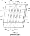
- FIG. 2 illustrates an interface region 200 of a conventional expansion card, such as the expansion card 100 of FIG. 1 .
- the interface region 200 includes four electrical pads, including two signal pads 202 and two ground pads 204 (collectively referred to as "contact pads” or “pads”).
- the signal pads 202 and the ground pads 204 are formed on a substrate 206 of a printed circuit board (PCB) having the interface region 200.
- the signal pads 202 and the ground pads 204 extend to the edge 206a of the substrate 206.
- the signal pads 202 carry one or more signals to and from the electrical circuit 205 on the printed circuit board and the corresponding bus (e.g., bus 102 of FIG. 1 ), within which the interface region 200 is inserted.
- Connector pins (e.g., connector pins 104 of FIG. 1 ) of the bus are configured to contact the signal pads 202 and the ground pads 204 at contact points 208 (represented by the dotted circles). Based on the lengths of the signal pads 202 and the ground pads 204, and the depth of the corresponding bus (e.g., bus 102 of FIG. 1 ), the contact points 208 are generally in the middle 214 of the signal pads 202 and the ground pads 204 (represented approximately by the dotted line).
- the electrical stubs are narrower than the signal electrical contacts.
- the ground electrical contacts have ends that longitudinally correspond with contact points of connector pins of a bus, with the expansion card interface fully inserted into the bus.
- the expansion card interface also includes ground stubs conductively isolated from the ground electrical contacts, with each of the ground stubs being aligned with a separate one of the ground electrical contacts.
- the signal pads 402 and the ground pads 404 can be formed initially by any conventional printed circuit board forming techniques, similar to the interface region 200 discussed above. Indeed, in one or more embodiments, the interface region 400 can be identical to the interface region 200, but the subsequent processing distinguishes the interface regions 200 and 400.
- the pads 402 and 404 can be divided into the respective electrical contacts 416 and 418, and the contact stubs 410 and 412, according to one or more processing steps.
- the dividing can be accomplished by mechanically modifying the pads 402 and 404 to form the first portions, corresponding to the electrical contacts 416 and 418, respectively, and the second portions, corresponding to the stubs 420 and 422, respectively.
- the mechanical modification can be any one or more mechanical processes that divide the pads 402 and 404 into conductively isolated first and second portions.
- the mechanical modification can be accomplished by drilling, such as back-drilling the pads 402 and 404.
- the mechanical modification can be accomplished by cutting the pads 402 and 404.
- the mechanical modification can be any other mechanical process(es) that can conductively separate the electrical contacts 416 and 418 from the stubs 410 and 412.
- the mechanical modification such as drilling or cutting
- the mechanical modification can modify only the pads 402 and 404 and not the substrate 406.
- the cutting may cut into and through the pads 402, pads 404, or both without cutting into the substrate 406.
- the mechanical modification can include partially modifying the substrate 406.
- the cutting can include partially cutting into the substrate 406.
- the pads 402 and 404 are divided into first and second portions, in one or more embodiments, less than all of the pads 402 and 404 can be divided into the first and second portions. For example, in one or more embodiments, only the signal pads 402 may be divided into the first and second portions. Alternatively, in one or more embodiments, only the ground pads 404 may be divided into the first and second portions. In one or more embodiments, less than all of the signal pads 402, ground pads 404, or both, may be divided into the respective first and second portions. Accordingly, the processes disclosed herein for dividing the pads can be applied to one or more signal pads, one or more ground pads, or both, to achieve better performance in signal margin by reducing or eliminating the effects of the contact stubs.
- FIG. 11 illustrates that sections 1002c and 1004c of the narrow portions 1002b and 1004b, respectively, can remain touching the wide portions 1002a and 1004a after dividing the pads 1002 and 1004.
- the sections 1002c and 1004c can remain touching the wide portions 1002a and 1004a. This can occur if, for example, the amounts of the pads 1002 and 1004 that are removed, or the locations where the pads 602 and 604 are divided, result in remaining portions of the sections 1002c and 1004c from the narrow portions 1002b and 1004b.
- such a high-frequency signal can be between 4-10 GHz, 4-20 GHz, or higher, including signals with frequencies at or greater than approximately 4 GHz, 5 GHz, 6 GHz, 7 GHz, 8 GHz, 9 GHz, 10 GHz, 11 GHz, 12 GHz, 13 GHz, 14 GHz, 15 GHz, 16 GHz, 17 GHz, 18 GHz, 19 GHz, and/or 20GHz.
- the divided contacts disclosed herein can be configured for use with such high-frequency signals.
Landscapes
- Engineering & Computer Science (AREA)
- Microelectronics & Electronic Packaging (AREA)
- Manufacturing & Machinery (AREA)
- Physics & Mathematics (AREA)
- Theoretical Computer Science (AREA)
- General Engineering & Computer Science (AREA)
- General Physics & Mathematics (AREA)
- Electromagnetism (AREA)
- Structure Of Printed Boards (AREA)
- Semiconductor Integrated Circuits (AREA)
Abstract
Description
- The present invention relates to connectors for computer systems and more specifically, to expansion card interfaces within computer systems for high-frequency signals.
- Expansion cards and other add-on cards can have interfaces, hereinafter expansion card interfaces. These expansion card interfaces are used extensively in computer systems. For example, many expansion cards (daughter cards) use expansion card interfaces for connecting to a bus on a main board (motherboard) of a computer system. One specific type of connector that can receive an expansion card is a peripheral component interconnect express (PCIe) connector, such as a
PCIe Gen 4 orGen 5 connector. -
FIG. 1 illustrates a conventional connection of anexpansion card 100 with abus 102, such as a PCIe bus. Thebus 102 includesconnector pins 104 within aslot 106 defined by ahousing 108. The connector pins 104 contact both sides of theexpansion card 100, when theexpansion card 100 is inserted into theslot 106. At least one side of theexpansion card 100 includes electrical pads (FIG. 2 ), which are commonly referred to as golden fingers. Theconnector pins 104 contact the electrical pads, which forms an electrical connection between theexpansion card 100 and thebus 102. -
FIG. 2 illustrates aninterface region 200 of a conventional expansion card, such as theexpansion card 100 ofFIG. 1 . Theinterface region 200 includes four electrical pads, including twosignal pads 202 and two ground pads 204 (collectively referred to as "contact pads" or "pads"). Thesignal pads 202 and theground pads 204 are formed on asubstrate 206 of a printed circuit board (PCB) having theinterface region 200. Thesignal pads 202 and theground pads 204 extend to theedge 206a of thesubstrate 206. Thesignal pads 202 carry one or more signals to and from theelectrical circuit 205 on the printed circuit board and the corresponding bus (e.g.,bus 102 ofFIG. 1 ), within which theinterface region 200 is inserted. - Connector pins (e.g.,
connector pins 104 ofFIG. 1 ) of the bus (e.g.,bus 102 ofFIG. 1 ) are configured to contact thesignal pads 202 and theground pads 204 at contact points 208 (represented by the dotted circles). Based on the lengths of thesignal pads 202 and theground pads 204, and the depth of the corresponding bus (e.g.,bus 102 ofFIG. 1 ), thecontact points 208 are generally in themiddle 214 of thesignal pads 202 and the ground pads 204 (represented approximately by the dotted line). - The lengths of the
signal pads 202 and theground pads 204, from generally thecontact points 208 to thedistal ends form signal stubs 210 andground stubs 212, respectively (collectively referred to as contact stubs or stubs). The lengths of thesignal pads 202 from generally thecontact points 208 to theproximal ends 202b, opposite from thedistal ends 202a, form signalelectrical contacts 216. The lengths of theground pads 204 from generally thecontact points 208 to theproximal ends 204b, opposite from thedistal ends 204a, form groundelectrical contacts 218. The signalelectrical contacts 216 and the groundelectrical contacts 218 are collectively referred to as electrical contacts. - The
signal stubs 210, theground stubs 212, or both can cause reflections in the signalelectrical contacts 216, the groundelectrical contacts 218, or both; thereby potentially reducing signal margins. For connections of high-frequency signals using the conventional expansion card withinterface region 200, the longer thesignal stubs 210, theground stubs 212, or both; the greater the reduction in the signal margin. -
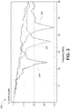
FIG. 3 illustrates aplot 300 of signal loss measurements for different lengths ofsignal stubs 210 and ground stubs 212 (both fromFIG. 2 ) as a function of signal frequency. Theline 302 represents an 80 millimeter (mm) stub; theline 304 represents a 110 mm stub; and theline 306 represents a 160 mm stub. As shown, the increase of signal loss measurements coincides with the increase in the length of the contact stubs. - Accordingly, there is a need for expansion card interfaces for use in connections of high-frequency signals that do not suffer from a reduction in signal margin, and methods for making such expansion card interfaces.
- According to one embodiment, the method of forming an expansion card interface for a printed circuit board is disclosed. The method includes forming electrical pads of the expansion card interface on a substrate. The method further includes dividing at least one electrical pad into a first portion and a second portion. The first portion is formed to be conductively coupled to a circuit on the printed circuit board, and the second portion is formed to be conductively isolated from the first portion.
- Another aspect of the embodiment includes the first portion being configured to contact a connector pin of a bus with the expansion card interface inserted into the bus. Still another aspect of the embodiment includes the dividing that occurs about 0.1 millimeters from a contact point between the connector pin and the at least one pad. Yet another aspect includes the dividing being accomplished by a mechanical modification of the least one pad to form the first portion and the second portion. The mechanical modification can include back-drilling of the at least one pad. The mechanical modification can alternatively include the cutting of the at least one pad. The cutting of the at least one pad can occur without cutting the printed circuit board. The dividing alternatively can be accomplished by a chemical modification of the at least one pad to form the first portion and the second portion. The chemical modification can include chemically etching the at least one pad. In still a further aspect, the forming of the at least one pad can include forming the at least one pad to include a narrow portion and a wide portion. In an additional aspect, the dividing of the at least one pad can occur on the narrow portion adjacent to the wide portion. In another aspect, the forming of the at least one pad includes providing an indicator, and the dividing of the at least one pad occurs at the indicator. In another aspect, the first portion can correspond substantially to the wide portion, and the second portion can correspond substantially to the narrow portion. In another aspect, the expansion card interface includes ground pads and signal pads. In still another aspect, the at least one pad includes all of the signal pads. In still another aspect, the at least one pad includes at least one of the signal pads.
- According to another embodiment, an expansion card interface for a printed circuit board is disclosed. The expansion card interface includes substrates having an edge, and signal electrical contacts configured to communicate one or more signals to and from the printed circuit board. The signal electrical contacts have ends that longitudinally correspond with contact points of connector pins of a bus, with the expansion card interface fully inserted into the bus. The expansion card interface also includes electrical stubs conductively isolated from the signal electrical contacts, with each of the electrical stubs being aligned with a separate one of the signal electrical contacts.
- According to another aspect, the electrical stubs are narrower than the signal electrical contacts. According to yet another aspect, the ground electrical contacts have ends that longitudinally correspond with contact points of connector pins of a bus, with the expansion card interface fully inserted into the bus. According to another aspect, the expansion card interface also includes ground stubs conductively isolated from the ground electrical contacts, with each of the ground stubs being aligned with a separate one of the ground electrical contacts.
- The above summary is not intended to represent each embodiment or every aspect of the present disclosure. Rather, the foregoing summary merely provides an example of some of the novel aspects and features set forth herein. The above features and advantages, and other features and advantages of the present disclosure, will be readily apparent from the following detailed description of representative embodiments and modes for carrying out the present invention, when taken in connection with the accompanying drawings and the appended claims.
- The disclosure, and its advantages and drawings, will be better understood from the following description of exemplary embodiments together with reference to the accompanying drawings. These drawings depict only exemplary embodiments and are, therefore, not to be considered as limitations on the scope of the various embodiments or claims.
-
FIG. 1 (PRIORART) illustrates a cross section of a conventional expansion card inserted into a bus. -
FIG. 2 (PRIORART) illustrates an interface region of a conventional expansion card. -
FIG. 3 illustrates signal loss measurements for different lengths of contact stubs of a conventional expansion card for a PCIe bus, as a function of signal frequency. -
FIG. 4 illustrates an interface region of an expansion card prior to dividing the contact pads, according to aspects of the present disclosure. -
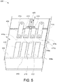
FIG. 5 illustrates the interface region of the expansion card ofFIG. 4 after dividing the contact pads, according to aspects of the present disclosure. -
FIG. 6 illustrates another interface region of an expansion card prior to dividing the contact pads, according to aspects of the present disclosure. -
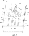
FIG. 7 illustrates the interface region of the expansion card ofFIG. 6 after dividing the contact pads, according to aspects of the present disclosure. -
FIG. 8 illustrates a plot of signal loss measurements of expansion card interfaces formed from the interface regions illustrated inFIG. 2 andFIG. 7 , according to aspects of the present disclosure. -
FIG. 9 illustrates a portion of the plot ofFIG. 8 , according to aspects of the present disclosure. -
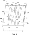
FIG. 10 illustrates another interface region of an expansion card prior to dividing the contact pads, according to aspects of the present disclosure. -
FIG. 11 illustrates the interface region of the expansion card ofFIG. 10 after dividing the contact pads, according to aspects of the present disclosure. - The various embodiments are described with reference to the attached figures, where like reference numerals are used throughout the figures to designate similar or equivalent elements. The figures are not drawn to scale, and they are provided merely to illustrate the instant invention. It should be understood that numerous specific details, relationships, and methods are set forth to provide a full understanding. One having ordinary skill in the relevant art, however, will readily recognize that the various embodiments can be practiced without one or more of the specific details, or with other methods. In other instances, well-known structures or operations are not shown in detail to avoid obscuring certain aspects of the various embodiments. The various embodiments are not limited by the illustrated ordering of acts or events, as some acts may occur in different orders and/or concurrently with other acts or events. Furthermore, not all illustrated acts or events are required to implement a methodology in accordance with the present invention.
- Elements and limitations that are disclosed, for example, in the Abstract, Summary, and Detailed Description sections, but not explicitly set forth in the claims, should not be incorporated into the claims, singly, or collectively, by implication, inference, or otherwise. For purposes of the present detailed description, unless specifically disclaimed, the singular includes the plural and vice versa. The word "including" means "including without limitation." Moreover, words of approximation, such as "about," "almost," "substantially," "approximately," and the like, can be used herein to mean "at," "near," or "nearly at," or "within 3-5% of," or "within acceptable manufacturing tolerances," or any logical combination thereof, for example.
- With regards to the present disclosure, the terms "computing device" or "computing system" or "computer system" refer to any electronically-powered or battery-powered equipment that has hardware, software, and/or firmware components, where the software and/or firmware components can be configured for operating features on the device. The term "operating environment" can refer to any operating system or environment that functions to allow software to run on a computer system.
- To solve the above-identified issue of the reduction in signal margin, electrical contacts and contact stubs are formed such that the contact stubs are conductively isolated from the electrical contacts. Pads are formed and subsequently divided into the electrical contacts and the contact stubs such that the contact stubs and the electrical contacts are conductively isolated. Because the electrical contacts are conductively isolated from the contact stubs, the contact stubs have no effect, or a reduced effect, on the signal margin.
-
FIG. 4 illustrates aninterface region 400 of an expansion card prior to dividing the contacts pads, according to aspects of the present disclosure. Theinterface region 400 includes four pads, which include twosignal pads 402 and twoground pads 404. Although only twosignal pads 402 and twoground pads 404 are shown inFIG. 4 , any expansion card formed withinterface region 400 can havemore signal pads 402, and can havemore ground pads 404. Thus, the twosignal pads 402 and the twoground pads 404 are shown for convenience only. - The
signal pads 402 and theground pads 404 are conventional golden fingers on asubstrate 406 of a printed circuit board. Thesignal pads 402 and theground pads 404 extend parallel to each other towards theedge 406a of thesubstrate 406. Thesignal pads 402 carry one or more signals to and from theelectrical circuit 405 on thesubstrate 406 and the corresponding bus (e.g.,bus 102 ofFIG. 1 ), within which theinterface region 400 is configured to be inserted. Theground pads 404 establish the ground between theinterface region 400 and the corresponding bus (e.g.,bus 102 ofFIG. 1 ). Thesignal pads 402 havedistal ends 402a andproximal ends 402b. Similarly, theground pads 404 havedistal ends 404a andproximal ends 404b. Thesignal pads 402 and theground pads 404 can be formed initially by any conventional printed circuit board forming techniques, similar to theinterface region 200 discussed above. Indeed, in one or more embodiments, theinterface region 400 can be identical to theinterface region 200, but the subsequent processing distinguishes theinterface regions - The
contact point 408 correspond to the locations at which connector pins (e.g., connector pins 104 ofFIG. 1 ) of a corresponding bus (e.g.,bus 102 ofFIG. 1 ) contact thesignal pads 402 and theground pads 404. Accordingly, the portions of thesignal pads 402 and theground pads 404 below the dottedline 414 correspond to the contact stubs. To remove the effects of such contact stubs, thesignal pads 402 and theground pads 404 are divided into two portions, as described in detail below. -
FIG. 5 illustrates theinterface region 400 of the expansion card ofFIG. 4 after dividing thecontact pads signal pads 402 and theground pads 404 are divided into two portions. The first portions correspond to the signalelectrical contacts 416 and the groundelectrical contacts 418, respectively. The second portions correspond to thesignal stubs 410 and the ground stubs 412, respectively. Because the signalelectrical contacts 416 are divided from the signal stubs 410, the signalelectrical contacts 416 are conductively isolated from the signal stubs 410. Similarly, because the groundelectrical contacts 418 are divided from the ground stubs 412, the groundelectrical contacts 418 are conductively isolated from the ground stubs 412. The signal stubs 410 and the ground stubs 412 also are conductively isolated from thecircuit 405 of the printed circuit board. The conductive isolation prevents or prohibits thesignal stubs 410 and the ground stubs 412 from affecting the signal margins. The connector pins (e.g., connector pins 104 ofFIG. 1 ) of the bus (e.g.,bus 102 ofFIG. 1 ) can still contact the signalelectrical contacts 416 and the groundelectrical contacts 418 with the expansion card inserted into the bus, as illustrated by thecontact point 408 still being aligned with the signalelectrical contacts 416 and the groundelectrical contacts 418. Indeed, the distal ends 416a of the signalelectrical contacts 416, and the distal ends 418a of the groundelectrical contacts 418, longitudinally correspond with the contact points 408 of the connector pins (e.g., connector pins 104 ofFIG. 1 ) of the bus (e.g.,bus 102 ofFIG. 1 ), with theinterface region 400 of the expansion card fully inserted into the bus. - The
pads electrical contacts contact stubs pads electrical contacts pads pads pads electrical contacts stubs - In one or more embodiments, the mechanical modification, such as drilling or cutting, can modify only the
pads substrate 406. For example, the cutting may cut into and through thepads 402,pads 404, or both without cutting into thesubstrate 406. However, in one or more alternative embodiments, the mechanical modification can include partially modifying thesubstrate 406. For example, the cutting can include partially cutting into thesubstrate 406. - In one or more embodiments, the dividing can be accomplished by chemically modifying the
pads electrical contacts stubs pads electrical contacts - Similar to the mechanical modification, in one or more embodiments, the chemical modification can modify only the
pads substrate 406. For example, the etching may etch into and through thepads 402,pads 404, or both; without etching into thesubstrate 406. This may occur based on thepads substrate 406. However, in one or more alternative embodiments, the chemical modification can include partially modifying thesubstrate 406. - In one or more embodiments, the dividing can be generally about 0.1 millimeters below the contact point 408 (i.e., towards the
ends FIG. 1 ) and thesignal pads 402 and theground pads 404, although other distances can be used. - Although all four of the
pads pads signal pads 402 may be divided into the first and second portions. Alternatively, in one or more embodiments, only theground pads 404 may be divided into the first and second portions. In one or more embodiments, less than all of thesignal pads 402,ground pads 404, or both, may be divided into the respective first and second portions. Accordingly, the processes disclosed herein for dividing the pads can be applied to one or more signal pads, one or more ground pads, or both, to achieve better performance in signal margin by reducing or eliminating the effects of the contact stubs. - Although the process of dividing the pads into first and second portions, described above with respect to
FIGS. 4 and5 , begins with a conventional configuration for thepads -
FIG. 6 illustrates aninterface region 600 of another expansion card prior to dividing the contact pads, according to aspects of the present disclosure. Theinterface region 600 includes four pads, which include twosignal pads 602 and twoground pads 604. Although only twosignal pads 602 and twoground pads 604 are shown inFIG. 6 , theinterface region 600 of the expansion card can havemore signal pads 602 andmore ground pads 604. Thus, the twosignal pads 602 and the twoground pads 604 are shown for convenience only. - Unlike the
signal pads 402 and theground pads 404 of theinterface region 400 inFIG. 4 , thesignal pads 602 and theground pads 604 havewide portions narrow portions wide portions signal pads 602 and theground pads 604 can be formed according to any conventional printed circuit board forming techniques, but withnarrow portions - The
narrow portions pads narrow portions narrow portions wide portions narrow portions pads -
FIG. 7 illustrates theinterface region 600 after dividing theelectrical pads 602 and 604 (both inFIG. 6 ), according to aspects of the present disclosure. Specifically, thesignal pads 602 are divided into two portions that correspond to the signalelectrical contacts 616 and thesignal stubs 610 generally, at where the widths transition from thenarrow portions 602b to thewide portions 602a. Theground pads 604 are divided into two portions that correspond to the groundelectrical contacts 618 and the ground stubs 612 generally, at where the widths transition from thenarrow portions 604b to thewide portions 604a. - The dividing can occur as disclosed above. Further, the dividing can similarly be generally about 0.1 millimeters below the
contact point 608 between the connector pin (FIG. 1 ) and the signalelectrical pads 602 and the groundelectrical pads 604, although other distances can be used. - Because the signal
electrical contacts 616 are divided from the signal stubs 610, the signalelectrical contacts 616 are conductively isolated from the signal stubs 610. Similarly, because the groundelectrical contacts 618 are divided from the ground stubs 612, the groundelectrical contacts 618 are conductively isolated from the ground stubs 612. The signal stubs 610 and the ground stubs 612 also are conductively isolated from thecircuit 605 of the printed circuit board. The conductive isolation prevents or prohibits the signal stubs 610, the ground stubs 612, or both, from affecting the signal margins. - The connector pins (e.g., connector pins 104 of
FIG. 1 ) of the bus (e.g.,bus 102 ofFIG. 1 ) can still connect to the signalelectrical contacts 616 and the groundelectrical contacts 618, as illustrated by thecontact point 608 still being aligned with the signalelectrical contacts 616 and the groundelectrical contacts 618. -
FIG. 8 illustrates aplot 800 comparing the signal loss measurements of theinterface region 600 ofFIG. 7 , after dividing the contact pads, versus theinterface region 200 ofFIG. 2 , according to aspects of the present disclosure.FIG. 9 illustrates aplot 900 of signal loss measurements fromFIG. 8 focused on the 0 to -10 dB range on the y-axis. Thelines 802 and 902 inFIGS. 8 and9 , respectively, illustrate the signal loss measurements of theinterface region 200. In contrast, thelines FIGS. 8 and9 , respectively, illustrate the signal loss measurements of theinterface region 600. Theplots interface region 600 versus theinterface region 200. Specifically, theline 802 shows a substantial amount of signal loss at higher frequencies for theinterface region 200. However, after dividing the contact pads, theline 804 shows that there is much less signal loss at those higher frequencies for theinterface region 600. -
FIG. 10 illustrates aninterface region 1000 of another expansion card prior to dividing the contact pads, according to aspects of the present disclosure. Theinterface region 1000 includes four pads, which include twosignal pads 1002 and twoground pads 1004. Although only twosignal pads 1002 and twoground pads 1004 are shown inFIG. 10 , theinterface region 1000 of the expansion card can havemore signal pads 1002 andmore ground pads 1004. Thus, the twosignal pads 1002 and the twoground pads 1004 are shown for convenience only. - Similar to the
signal pads 602 and theground pads 604 of theinterface region 600 inFIG. 6 , thesignal pads 1002 and theground pads 1004 havewide portions narrow portions wide portions signal pads 1002 and theground pads 1004 can be formed according to any conventional printed circuit board forming techniques, but with the change of having thenarrow portions - Further, the
narrow portions indicators 1020, or otherwise include theindicators 1020. Theindicators 1020 visually mark where to divide thepads narrow portions indicators 1020 can be any type of visual indicia that marks where to divide thepads indicators 1020 can instead be plus signs, the letter X, etc., printed or otherwise provided on thepads pads Indicators 1020 can be formed from the same material aspads FIG. 10 ; or can be formed of another material, such as an ink that can be applied topads substrate 1006. Further, although illustrated in reference to thepads narrow portions wide portions indicators 1020 can be present on any type of contact pads, such as on thecontact pads interface region 400 ofFIG. 4 . -
FIG. 11 illustrates theinterface region 1000 after dividing thepads indicators 1020, according to aspects of the present disclosure. Specifically, thesignal pads 1002 are divided into two portions that correspond to the signalelectrical contacts 1016 and thesignal stubs 1010, generally at where the widths transition from thenarrow portions 1002b to thewide portions 1002a. Similarly, theground pads 1004 are divided into two portions that correspond to the groundelectrical contacts 1018 and theground stubs 1012, generally at where the widths transition from thenarrow portions 1004b to thewide portions 1004a. - The dividing can occur as disclosed above. Further, the dividing can similarly be generally about 0.1 millimeters below the
contact point 1008, i.e., the points where the connector pins (e.g.,connector pin 104 ofFIG. 1 ) contact thesignal pads 1002 and the ground pads 1004-although other distances can be used. - Further,
FIG. 11 illustrates thatsections narrow portions wide portions pads sections wide portions pads pads sections narrow portions - Because the signal
electrical contacts 1016 are divided from thesignal stubs 1010, the signalelectrical contacts 1016 are conductively isolated from thesignal stubs 1010. Similarly, because the groundelectrical contacts 1018 are divided from theground stubs 1012, the groundelectrical contacts 1018 are conductively isolated from theground stubs 1012. Thesignal stubs 1010 and theground stubs 1012 also are conductively isolated from thecircuit 1005 of the printed circuit board. The conductive isolation prevents or prohibits thesignal stubs 1010, theground stubs 1012, or both from affecting the signal margins. - The benefits described herein with reference to divided contacts, such as those described with reference to
FIGS. 8 ,9 , and11 , can be especially pronounced when high frequency signals are being used. In some cases, such a high-frequency signal can be between 4-10 GHz, 4-20 GHz, or higher, including signals with frequencies at or greater than approximately 4 GHz, 5 GHz, 6 GHz, 7 GHz, 8 GHz, 9 GHz, 10 GHz, 11 GHz, 12 GHz, 13 GHz, 14 GHz, 15 GHz, 16 GHz, 17 GHz, 18 GHz, 19 GHz, and/or 20GHz. In some cases, the divided contacts disclosed herein can be configured for use with such high-frequency signals. - While various embodiments of the present invention have been described above, it should be understood that they have been presented by way of example only, and not limitation. Numerous changes to the disclosed embodiments can be made in accordance with the disclosure herein without departing from the spirit or scope. Thus, the breadth and scope of the present invention should not be limited by any of the above described embodiments. Rather, the scope of the invention should be defined in accordance with the following claims and their equivalents.
- Although the invention has been illustrated and described with respect to one or more implementations, equivalent alterations, and modifications will occur to others skilled in the art upon the reading and understanding of this specification and the annexed drawings. In addition, while a particular feature of the invention may have been disclosed with respect to only one of several implementations, such feature may be combined with one or more other features of the other implementations as may be desired and advantageous for any given or particular application.
- The terminology used herein is for the purpose of describing particular embodiments only and is not intended to be limiting. As used herein, the singular forms "a," "an," and "the" are intended to include the plural forms as well, unless the context clearly indicates otherwise. Furthermore, to the extent that the terms "including," "includes," "having," "has," "with," or variants thereof are used in either the detailed description and/or the claims, such terms are intended to be inclusive in a manner similar to the term "comprising."
- Unless otherwise defined, all terms (including technical and scientific terms) used herein have the same meaning as commonly understood by one of ordinary skill in the art to which this invention belongs. Furthermore, terms, such as those defined in commonly used dictionaries, should be interpreted as having a meaning that is consistent with their meaning in the context of the relevant art and will not be interpreted in an idealized or overly formal sense unless expressly so defined herein.
Claims (15)
- A method of forming an expansion card interface for a printed circuit board, the method comprising:forming pads of the expansion card interface on a substrate (406); anddividing at least one pad into a first portion and a second portion, with the first portion conductively coupled to a circuit (405) on the printed circuit board, and the second portion conductively isolated from the first portion.
- The method of claim 1, wherein the first portion is configured to contact a connector pin (104) of a bus (102) with the expansion card interface inserted into the bus (102), and the dividing occurs about 0.1 millimeters from a contact point (408) between the connector pin (104) and the at least one pad.
- The method of claim 1 or 2, wherein the dividing comprises mechanically modifying the at least one pad to form the first portion and the second portion.
- The method of claim 3, wherein the mechanical modification is back-drilling the at least one pad.
- The method of claim 3, wherein the mechanical modification is cutting the at least one pad, and the cutting of the at least one pad occurs without cutting the printed circuit board.
- The method of anyone of the claims 1 to 5, wherein the dividing comprises chemically modifying the at least one pad to form the first portion and the second portion, and the chemical modification is chemically etching the at least one pad.
- The method of anyone of the claims 1 to 6, wherein the forming of the at least one pad includes forming the at least one pad to include a narrow portion (602b) and a wide portion (602a).
- The method of claim 7, wherein the dividing of the at least one pad occurs on the narrow portion (602b) adjacent to the wide portion (602a).
- The method of claim 7 or 8, wherein the forming of the at least one pad includes providing an indicator (1020), and the dividing of the at least one pad occurs as the indicator (1020).
- The method of anyone of the claims 7 to 9, wherein the first portion corresponds substantially to the wide portion (602a), and the second portion corresponds substantially to the narrow portion (602b).
- The method of anyone of the claims 1 to 10, wherein the expansion card interface includes ground pads (404) and signal pads (402), and the at least one pad is all of the signal pads (402).
- The method of claim 11, wherein the at least one pad comprises at least one of the signal pads (402).
- An expansion card interface for a printed circuit board, the expansion card interface comprising:a substrate (406) having an edge (406a);signal electrical contacts (416) configured to communicate one or more signals to and from a circuit (405) on the printed circuit board, the signal electrical contacts (416) having ends that longitudinally correspond with contact points (408) of connector pins (104) of a bus (102) when the expansion card interface is fully inserted into a slot (106); andelectrical stubs conductively isolated from the signal electrical contacts (416), with each of the electrical stubs being aligned with a separate one of the signal electrical contacts (416).
- The expansion card interface of claim 13, wherein the electrical stubs are narrower than the signal electrical contacts (416).
- The expansion card interface of claim 13 or 14, further comprising:ground electrical contacts (418) having ends that longitudinally correspond with the contact points (408) of the connector pins (104) of the bus (102), with the expansion card interface fully inserted into the bus (102); andground stubs (412) conductively isolated from the ground electrical contacts (418), with each of the ground stubs (412) being aligned with a separate one of the ground electrical contacts (418).
Applications Claiming Priority (2)
| Application Number | Priority Date | Filing Date | Title |
|---|---|---|---|
| US201962853956P | 2019-05-29 | 2019-05-29 | |
| US16/714,181 US10999929B2 (en) | 2019-05-29 | 2019-12-13 | Expansion card interfaces for high-frequency signals and methods of making the same |
Publications (1)
| Publication Number | Publication Date |
|---|---|
| EP3745829A1 true EP3745829A1 (en) | 2020-12-02 |
Family
ID=69804433
Family Applications (1)
| Application Number | Title | Priority Date | Filing Date |
|---|---|---|---|
| EP20158570.0A Pending EP3745829A1 (en) | 2019-05-29 | 2020-02-20 | Expansion card interfaces for high-frequency signals and methods of making the same |
Country Status (5)
| Country | Link |
|---|---|
| US (1) | US10999929B2 (en) |
| EP (1) | EP3745829A1 (en) |
| JP (1) | JP6929400B2 (en) |
| CN (1) | CN112020201B (en) |
| TW (1) | TWI776119B (en) |
Citations (3)
| Publication number | Priority date | Publication date | Assignee | Title |
|---|---|---|---|---|
| US5492478A (en) * | 1991-07-05 | 1996-02-20 | Mod-Tap W Corp. | Electrical connection system with alternatively positionable connector |
| US6115260A (en) * | 1998-10-01 | 2000-09-05 | Mitsubishi Denki Kabushiki Kaisha | Memory module with obstacle removing terminal structure |
| US20180138637A1 (en) * | 2016-11-11 | 2018-05-17 | Tyco Electronics (Shanghai) Co. Ltd. | Connector and Connector Assembly |
Family Cites Families (46)
| Publication number | Priority date | Publication date | Assignee | Title |
|---|---|---|---|---|
| JPH0652941A (en) | 1992-07-31 | 1994-02-25 | Pfu Ltd | Connector |
| JPH0654133U (en) | 1992-12-28 | 1994-07-22 | ニスカ株式会社 | Connection cable |
| JPH09321165A (en) * | 1996-05-27 | 1997-12-12 | Toshiba Corp | Semiconductor device substrate, semiconductor device, card type module, and information storage device |
| JP3815936B2 (en) * | 2000-01-25 | 2006-08-30 | 株式会社ルネサステクノロジ | IC card |
| US20030112613A1 (en) * | 2002-10-22 | 2003-06-19 | Hitachi, Ltd. | IC card |
| KR100335716B1 (en) * | 2000-05-23 | 2002-05-08 | 윤종용 | Memory Card |
| JP2002245997A (en) | 2001-02-15 | 2002-08-30 | Taiyo Yuden Co Ltd | Hybrid module connection adapter and battery pack |
| DE10208737B4 (en) * | 2002-02-28 | 2008-08-14 | Qimonda Ag | Adapter device for memory modules |
| US6589061B1 (en) * | 2002-03-07 | 2003-07-08 | Hon Hai Precision Ind. Co., Ltd. | Printed circuit board for straddle mount electrical connector and method for pasting the same |
| JP4094394B2 (en) * | 2002-09-30 | 2008-06-04 | 株式会社ルネサステクノロジ | IC card and manufacturing method thereof |
| TWI220931B (en) * | 2003-04-23 | 2004-09-11 | Toppoly Optoelectronics Corp | Method of testing FPC bonding yield and FPC having testing pads thereon |
| KR100541544B1 (en) * | 2003-05-06 | 2006-01-10 | 삼성전자주식회사 | Memory system with improved signal fidelity |
| JP2005122657A (en) * | 2003-10-20 | 2005-05-12 | Renesas Technology Corp | IC card |
| JP4651332B2 (en) * | 2004-04-26 | 2011-03-16 | ルネサスエレクトロニクス株式会社 | Memory card |
| US20050281010A1 (en) * | 2004-06-18 | 2005-12-22 | Super Talent Electronics, Inc. | Contact pad arrangement for integrated SD/MMC system |
| US7032827B2 (en) * | 2004-06-18 | 2006-04-25 | Super Talent Electronics, Inc. | Combination SD/MMC flash memory card with thirteen contact pads |
| US7009846B1 (en) * | 2004-07-30 | 2006-03-07 | Super Talent Electronics, Inc. | 13-Pin socket for combination SD/MMC flash memory system |
| JPWO2006033156A1 (en) * | 2004-09-24 | 2008-05-15 | 株式会社ルネサステクノロジ | Semiconductor device |
| KR100590477B1 (en) * | 2004-12-22 | 2006-06-19 | 삼성전자주식회사 | Memory module and motherboard connection structure using the edge of motherboard and memory module |
| JP2006236261A (en) * | 2005-02-28 | 2006-09-07 | Renesas Technology Corp | Memory card adapter and memory card |
| CN2796303Y (en) * | 2005-03-29 | 2006-07-12 | 亿光电子工业股份有限公司 | Printed Circuit Board Pad Structure |
| JP4864346B2 (en) * | 2005-05-18 | 2012-02-01 | ソニー株式会社 | Memory card and card adapter |
| JP2007128812A (en) | 2005-11-07 | 2007-05-24 | Matsushita Electric Works Ltd | Connector assembly for connecting substrate |
| JP4843447B2 (en) * | 2006-03-31 | 2011-12-21 | 株式会社東芝 | Semiconductor device and memory card using the same |
| JP2008004380A (en) | 2006-06-22 | 2008-01-10 | Sumitomo Wiring Syst Ltd | Connector for circuit board |
| CN101512559A (en) * | 2006-09-27 | 2009-08-19 | 株式会社瑞萨科技 | IC card and IC card socket |
| JP4930021B2 (en) * | 2006-12-06 | 2012-05-09 | ソニー株式会社 | Memory card |
| TWI334320B (en) * | 2007-07-16 | 2010-12-01 | Nanya Technology Corp | Fabricating method of gold finger of circuit board |
| US7845985B2 (en) * | 2008-03-04 | 2010-12-07 | Molex Incorporated | Co-edge connector |
| US7862381B2 (en) * | 2008-09-26 | 2011-01-04 | Sandisk Corporation | Connector block feature |
| US7909611B2 (en) * | 2008-09-26 | 2011-03-22 | Sandisk Corporation | Method for preventing damage to a memory card |
| CN103025082B (en) * | 2011-09-21 | 2015-08-05 | 英业达股份有限公司 | A method of manufacturing a printed circuit board and a printed circuit board structure |
| US20170197239A1 (en) * | 2012-01-10 | 2017-07-13 | Seoul Laser Dieboard System Co., Ltd. | Multiple broaching marks on rules |
| TWI616134B (en) * | 2013-03-20 | 2018-02-21 | Ground pattern structure of circuit board high frequency pad area | |
| US20150257316A1 (en) * | 2014-03-07 | 2015-09-10 | Bridge Semiconductor Corporation | Method of making thermally enhanced wiring board having isolator incorporated therein |
| KR102168170B1 (en) * | 2014-06-30 | 2020-10-20 | 삼성전자주식회사 | Memory card |
| KR102284654B1 (en) * | 2014-07-02 | 2021-08-03 | 삼성전자 주식회사 | Memory card |
| US10157678B2 (en) * | 2014-08-12 | 2018-12-18 | Samsung Electronics Co., Ltd. | Memory card |
| CA2941284C (en) * | 2015-09-08 | 2022-04-05 | Ross Video Limited | Circuit board pad layout and mechanical retainer |
| US9929511B2 (en) * | 2016-03-18 | 2018-03-27 | Intel Corporation | Shielded high density card connector |
| JP2017174641A (en) * | 2016-03-24 | 2017-09-28 | 株式会社ジャパンディスプレイ | Manufacturing method of display device |
| KR102646895B1 (en) * | 2016-09-29 | 2024-03-12 | 삼성전자주식회사 | Memory cards and storage systems including the same |
| CN106455343B (en) | 2016-11-30 | 2019-02-05 | 深圳市景旺电子股份有限公司 | A kind of minimizing technology of gold finger lead |
| KR102444234B1 (en) * | 2018-01-03 | 2022-09-16 | 삼성전자주식회사 | Memory Cards and Electronic Systems |
| KR102440366B1 (en) * | 2018-01-04 | 2022-09-05 | 삼성전자주식회사 | Memory card and electronic apparatus including the same |
| JP2020003875A (en) * | 2018-06-25 | 2020-01-09 | キオクシア株式会社 | Semiconductor storage device |
-
2019
- 2019-12-13 US US16/714,181 patent/US10999929B2/en active Active
-
2020
- 2020-01-17 TW TW109101699A patent/TWI776119B/en active
- 2020-02-20 EP EP20158570.0A patent/EP3745829A1/en active Pending
- 2020-02-25 JP JP2020029182A patent/JP6929400B2/en active Active
- 2020-02-25 CN CN202010116560.9A patent/CN112020201B/en active Active
Patent Citations (3)
| Publication number | Priority date | Publication date | Assignee | Title |
|---|---|---|---|---|
| US5492478A (en) * | 1991-07-05 | 1996-02-20 | Mod-Tap W Corp. | Electrical connection system with alternatively positionable connector |
| US6115260A (en) * | 1998-10-01 | 2000-09-05 | Mitsubishi Denki Kabushiki Kaisha | Memory module with obstacle removing terminal structure |
| US20180138637A1 (en) * | 2016-11-11 | 2018-05-17 | Tyco Electronics (Shanghai) Co. Ltd. | Connector and Connector Assembly |
Also Published As
| Publication number | Publication date |
|---|---|
| TW202044966A (en) | 2020-12-01 |
| JP6929400B2 (en) | 2021-09-01 |
| US20200383205A1 (en) | 2020-12-03 |
| CN112020201A (en) | 2020-12-01 |
| JP2020194526A (en) | 2020-12-03 |
| US10999929B2 (en) | 2021-05-04 |
| CN112020201B (en) | 2022-04-12 |
| TWI776119B (en) | 2022-09-01 |
Similar Documents
| Publication | Publication Date | Title |
|---|---|---|
| US6966784B2 (en) | Flexible cable interconnect assembly | |
| US3973817A (en) | Interconnection of circuit boards | |
| US6152742A (en) | Surface mounted electrical connector | |
| CN104871654B (en) | The structure of the electronic substrate and its joint connection | |
| WO2001093375A2 (en) | Connector with terminals having increased capacitance | |
| US7048585B2 (en) | High speed connector assembly | |
| CN109831871B (en) | Chip on film packaged flexible circuit board, flexible circuit board and manufacturing method thereof | |
| US7666001B2 (en) | Circuit connection structure and printed circuit board | |
| US20140285280A1 (en) | Grounding pattern structure for high-frequency connection pad of circuit board | |
| EP3675605A1 (en) | Golden finger connector for high speed differential signal interconnections | |
| CN219874136U (en) | High-frequency signal transmission device | |
| US6000950A (en) | Connector for flexible printed cards | |
| US7390193B2 (en) | Printed circuit board assembly | |
| JP6765640B2 (en) | Connector and cable with connector | |
| US10999929B2 (en) | Expansion card interfaces for high-frequency signals and methods of making the same | |
| EP3469862A1 (en) | Electrical contact pad for electrically contacting a connector | |
| US20110294356A1 (en) | Connector | |
| CN111628318B (en) | Expansion card interface for high frequency signals | |
| JP2003178827A (en) | Multi-connector for high-speed communication apparatus and mounting method of multi-connector for high-speed communication apparatus and printed circuit board | |
| US11394146B2 (en) | Treated connection pins for high speed expansion sockets | |
| JPH11204204A (en) | connector | |
| CN109546389A (en) | Back panel connector | |
| US20060121798A1 (en) | One-piece multi-shank contact spring for miniature plug connectors | |
| JP2004039405A (en) | Contact module | |
| JPH08315891A (en) | Connector for inserting/extracting hot-line |
Legal Events
| Date | Code | Title | Description |
|---|---|---|---|
| PUAI | Public reference made under article 153(3) epc to a published international application that has entered the european phase |
Free format text: ORIGINAL CODE: 0009012 |
|
| STAA | Information on the status of an ep patent application or granted ep patent |
Free format text: STATUS: THE APPLICATION HAS BEEN PUBLISHED |
|
| STAA | Information on the status of an ep patent application or granted ep patent |
Free format text: STATUS: REQUEST FOR EXAMINATION WAS MADE |
|
| AK | Designated contracting states |
Kind code of ref document: A1 Designated state(s): AL AT BE BG CH CY CZ DE DK EE ES FI FR GB GR HR HU IE IS IT LI LT LU LV MC MK MT NL NO PL PT RO RS SE SI SK SM TR |
|
| AX | Request for extension of the european patent |
Extension state: BA ME |
|
| 17P | Request for examination filed |
Effective date: 20201110 |
|
| RBV | Designated contracting states (corrected) |
Designated state(s): AL AT BE BG CH CY CZ DE DK EE ES FI FR GB GR HR HU IE IS IT LI LT LU LV MC MK MT NL NO PL PT RO RS SE SI SK SM TR |
|
| STAA | Information on the status of an ep patent application or granted ep patent |
Free format text: STATUS: EXAMINATION IS IN PROGRESS |
|
| 17Q | First examination report despatched |
Effective date: 20210204 |