EP3745171B1 - A temperature compensation module mounted in arrayed waveguide grating and a method of manufacturing an athermal arrayed waveguide grating - Google Patents
A temperature compensation module mounted in arrayed waveguide grating and a method of manufacturing an athermal arrayed waveguide grating Download PDFInfo
- Publication number
- EP3745171B1 EP3745171B1 EP19743607.4A EP19743607A EP3745171B1 EP 3745171 B1 EP3745171 B1 EP 3745171B1 EP 19743607 A EP19743607 A EP 19743607A EP 3745171 B1 EP3745171 B1 EP 3745171B1
- Authority
- EP
- European Patent Office
- Prior art keywords
- awg
- fixing part
- waveguide
- temperature compensation
- compensation module
- Prior art date
- Legal status (The legal status is an assumption and is not a legal conclusion. Google has not performed a legal analysis and makes no representation as to the accuracy of the status listed.)
- Active
Links
Images







Classifications
-
- G—PHYSICS
- G02—OPTICS
- G02B—OPTICAL ELEMENTS, SYSTEMS OR APPARATUS
- G02B6/00—Light guides; Structural details of arrangements comprising light guides and other optical elements, e.g. couplings
- G02B6/10—Light guides; Structural details of arrangements comprising light guides and other optical elements, e.g. couplings of the optical waveguide type
- G02B6/12—Light guides; Structural details of arrangements comprising light guides and other optical elements, e.g. couplings of the optical waveguide type of the integrated circuit kind
- G02B6/12007—Light guides; Structural details of arrangements comprising light guides and other optical elements, e.g. couplings of the optical waveguide type of the integrated circuit kind forming wavelength selective elements, e.g. multiplexer, demultiplexer
- G02B6/12009—Light guides; Structural details of arrangements comprising light guides and other optical elements, e.g. couplings of the optical waveguide type of the integrated circuit kind forming wavelength selective elements, e.g. multiplexer, demultiplexer comprising arrayed waveguide grating [AWG] devices, i.e. with a phased array of waveguides
- G02B6/12026—Light guides; Structural details of arrangements comprising light guides and other optical elements, e.g. couplings of the optical waveguide type of the integrated circuit kind forming wavelength selective elements, e.g. multiplexer, demultiplexer comprising arrayed waveguide grating [AWG] devices, i.e. with a phased array of waveguides characterised by means for reducing the temperature dependence
- G02B6/1203—Light guides; Structural details of arrangements comprising light guides and other optical elements, e.g. couplings of the optical waveguide type of the integrated circuit kind forming wavelength selective elements, e.g. multiplexer, demultiplexer comprising arrayed waveguide grating [AWG] devices, i.e. with a phased array of waveguides characterised by means for reducing the temperature dependence using mounting means, e.g. by using a combination of materials having different thermal expansion coefficients
-
- G—PHYSICS
- G02—OPTICS
- G02B—OPTICAL ELEMENTS, SYSTEMS OR APPARATUS
- G02B6/00—Light guides; Structural details of arrangements comprising light guides and other optical elements, e.g. couplings
- G02B6/10—Light guides; Structural details of arrangements comprising light guides and other optical elements, e.g. couplings of the optical waveguide type
- G02B6/12—Light guides; Structural details of arrangements comprising light guides and other optical elements, e.g. couplings of the optical waveguide type of the integrated circuit kind
- G02B6/12007—Light guides; Structural details of arrangements comprising light guides and other optical elements, e.g. couplings of the optical waveguide type of the integrated circuit kind forming wavelength selective elements, e.g. multiplexer, demultiplexer
- G02B6/12009—Light guides; Structural details of arrangements comprising light guides and other optical elements, e.g. couplings of the optical waveguide type of the integrated circuit kind forming wavelength selective elements, e.g. multiplexer, demultiplexer comprising arrayed waveguide grating [AWG] devices, i.e. with a phased array of waveguides
- G02B6/12033—Light guides; Structural details of arrangements comprising light guides and other optical elements, e.g. couplings of the optical waveguide type of the integrated circuit kind forming wavelength selective elements, e.g. multiplexer, demultiplexer comprising arrayed waveguide grating [AWG] devices, i.e. with a phased array of waveguides characterised by means for configuring the device, e.g. moveable element for wavelength tuning
-
- G—PHYSICS
- G02—OPTICS
- G02B—OPTICAL ELEMENTS, SYSTEMS OR APPARATUS
- G02B6/00—Light guides; Structural details of arrangements comprising light guides and other optical elements, e.g. couplings
- G02B6/10—Light guides; Structural details of arrangements comprising light guides and other optical elements, e.g. couplings of the optical waveguide type
- G02B6/12—Light guides; Structural details of arrangements comprising light guides and other optical elements, e.g. couplings of the optical waveguide type of the integrated circuit kind
- G02B6/13—Integrated optical circuits characterised by the manufacturing method
-
- G—PHYSICS
- G02—OPTICS
- G02B—OPTICAL ELEMENTS, SYSTEMS OR APPARATUS
- G02B6/00—Light guides; Structural details of arrangements comprising light guides and other optical elements, e.g. couplings
- G02B6/10—Light guides; Structural details of arrangements comprising light guides and other optical elements, e.g. couplings of the optical waveguide type
- G02B6/12—Light guides; Structural details of arrangements comprising light guides and other optical elements, e.g. couplings of the optical waveguide type of the integrated circuit kind
- G02B2006/12083—Constructional arrangements
- G02B2006/12107—Grating
-
- G—PHYSICS
- G02—OPTICS
- G02B—OPTICAL ELEMENTS, SYSTEMS OR APPARATUS
- G02B6/00—Light guides; Structural details of arrangements comprising light guides and other optical elements, e.g. couplings
- G02B6/10—Light guides; Structural details of arrangements comprising light guides and other optical elements, e.g. couplings of the optical waveguide type
- G02B6/12—Light guides; Structural details of arrangements comprising light guides and other optical elements, e.g. couplings of the optical waveguide type of the integrated circuit kind
Definitions
- the present disclosure relates to athermal arrayed waveguide grating (AWG) using a precise parallel movement module and a manufacturing method therefor, and more particularly, to athermal arrayed waveguide grating (AWG) with a temperature compensation module capable of precise horizontal movement to uniformly maintain the wavelength irrespective of outside temperature changes and a manufacturing method therefor.
- WDM wavelength division multiplexing
- planar lightwave circuits having optical waveguides on a plate of silica by a combination of optical fiber technology and large scale integration (LSI) technology are used as wavelength division multiplexers/demultiplexers.
- the PLC e.g., arrayed waveguide gratings (AWGs), splitters
- AWGs arrayed waveguide gratings
- the changes in refractive index n lead to changes in the path L of light that determines the wavelength, and changes in wavelength ⁇ occur in the channel of each output port.
- AWGs arrayed waveguide gratings
- FIG. 1 a general AWG will be described with reference to FIG. 1 .
- FIG. 1 illustrates the structure of the general AWG.
- the AWG includes an input waveguide 1, an input slab waveguide 2, an array waveguide 3, an output slab waveguide 4 and an output waveguide 5.
- An optical signal inputted to the input waveguide 1 is split at each wavelength ⁇ 1, ⁇ 2, ..., ⁇ n and outputted to the output waveguide 5. That is, when wavelength ⁇ 1 is allocated to #1 channel, it is necessary that the wavelength ⁇ 1 is outputted to the output waveguide 5 despite changes in the surrounding environment.
- the refractive index changes with temperature, and as the refractive index changes, the wavelength of the AWG changes as well.
- the wavelength ⁇ 1 is allocated to #1 channel, as the temperature changes, an error may occur, for example, wavelength ⁇ 2 may be outputted.
- a cutting plane 6 for dividing a substrate into two parts 10a, 10b is included to compensate for temperature changes.
- the AWG of FIG. 1 compensates for wavelength with the changes in temperature to prevent the changes in wavelength at the output port by allowing the first sub chip 10a including the input waveguide 1 to move along the cutting plane 6.
- a material having the coefficient of thermal expansion that matches the change in wavelength is machined and used, and such a material is referred to as a temperature compensation material or a thermal compensation material and primarily includes metals having a high coefficient of thermal expansion.
- the PLC that is one of optical communication components requires very precise alignment with the alignment tolerance of 0.5micrometers. Re-aligning the first sub chip 10a and the second sub chip 10b of the AWG cut to achieve temperature insensitivity within the tolerance causes a challenging technical problem.
- KR 2006 0025984 A discloses an optical integrated circuits having a gap traversing the lens or the waveguide grating and an actuator that controllably positions the optical integrated circuit on each side of the gap. As a result, the thermal sensitivity of the optical integrated circuits, for example, arrayed waveguide gratings, is mitigated.
- US 2008/135169 A1 discloses a method to compensate temperature dependency of center wavelength by adjusting optical input position passively by cutting the interface between the input slap waveguide of AWG and the stripe waveguide circuit connected to the input slab on a AWG chip, followed by attaching the lateral sliding rod which has the larger CTE (Coefficient of Thermal Expansion) than AWG chip substrate.
- CTE Coefficient of Thermal Expansion
- US 2002/181871 A1 discloses an arrayed waveguide grating, in which at least one of two slab waveguides constituting the arrayed waveguide grating is cut and separated together with a substrate on a cross separating face, a slide moving member is arranged over a waveguide forming area formed on the substrate including the separating slab waveguide and a waveguide forming area formed on the substrate including the separating slab waveguide.
- the athermal arrayed wavelength grating comprises a base plate, an arrayed wavelength grating chip and a temperature compensation component, wherein the base plate comprises a first base plate part and a second base plate part; the temperature compensation component enables the first base plate part and the second base plate part which form the base plate to relatively move in parallel in a plane where the base plate is located; the arrayed wavelength grating chip is cut into a first chip part and a second chip part which move relative to each other; the first chip part and the second chip part are respectively fixed on the first base plate part and the second base plate part.
- the present invention as defined by claim 1 is directed to a temperature compensation module mounted in an arrayed waveguide grating (AWG) in which a cutting plane is aligned within the tolerance using the temperature compensation module capable of precise horizontal movement to facilitate the alignment of the cutting plane of the athermal AWG and a manufacturing method of an athermal AWG using the temperature compensation module as defined by claim 11.
- AWG arrayed waveguide grating
- the present disclosure provides athermal arrayed waveguide grating (AWG) that facilitates the alignment of the cutting plane of the AWG and achieves precise horizontal movement without a change in vertical gap and difference of the cutting plane through the temperature compensation module capable of precise horizontal movement.
- AWG athermal arrayed waveguide grating
- first means first, second, and the like.
- the athermal AWG is cut between an input waveguide 1 and an input slab waveguide 2 or into the input slab waveguide 2 to compensate for changes in the center wavelength by changing the location of incoming light with the changes in temperature.
- a temperature compensation module for easy alignment of the cutting plane of the athermal AWG and precise horizontal movement with the expansion/contraction of a thermal compensation material is shown in FIGS. 2 to 5 below.
- FIG. 2 illustrates the basic structure of the temperature compensation module 20 according to an embodiment of the present disclosure.
- the basic structure of the temperature compensation module 20 includes a base 21 and a moving member 25.
- the base 21 is attached to an AWG substrate to facilitate the alignment between the cut parts of the AWG and assist the precise horizontal movement of the cut part of the AWG with the expansion and contraction of the moving member 25 attached to a portion of the base 21.
- the base 21 includes a first fixing part 22, a second fixing part 23 and an elastic part 24 connecting the first fixing part 22 and the second fixing part 23.
- the base 21 may be integrally formed by machining such that the base 21 includes the first fixing part 22, the second fixing part 23 and the elastic part 24 from one raw material, and is easy to machine in order to change the shape.
- the base 21 is made of a material having a large difference in coefficient of thermal expansion from the moving member 25 of the thermal compensation material, it is possible to maximize the temperature compensation effect.
- the moving member 25 uses a metal having a high coefficient of thermal expansion.
- the base 21 may be made of, for example, metal, plastic, silicon and silica-based materials having a lower coefficient of thermal expansion.
- the base 21 may be made of the same material as the AWG substrate. Through this, it is possible to prevent twists due to different coefficients of thermal expansion when the base 21 and the AWG substrate are attached.
- the first fixing part 22 and the second fixing part 23 may be fixed and attached to the AWG.
- an adhesive such as epoxy may be used to fix and attach the first fixing part 22 and the second fixing part 23 to the AWG chip, but fixing is not necessarily conducted only by the adhesive.
- Various types of members may be used to fix and attach the first fixing part 22 and the second fixing part 23 to the AWG chip.
- the moving member 25 is attached to the first fixing part 22 to cause linear movements of the separated part of the AWG through expansion/contraction with temperature, and through this, to compensate for changes in the optical properties with temperature.
- the elastic part 24 is formed with elasticity such that the elastic part 24 deforms to make linear movements as the moving member 25 expands/contracts, but restores to the original shape.
- the elastic part 24 is in the shape of a leaf spring, and includes a support 26 machined in a very small thickness and a leg 27 connecting two ends of the support 26 to the first fixing part 22 and the second fixing part 23 respectively.
- the support 26 and the horizontal portion of the leg 27 parallel to the support 26 may be machined in a very small thickness such that they have the width of a few mm or less according to the required elasticity.
- the upper and lower plates (the first and second fixing parts) with the ' ' shaped elastic part 24 connected on the left and right sides in a symmetrical structure achieve precise horizontal movements due to offset of two circular movements.
- the elastic part 24 of vertically thick structure suppresses vertical movements, so there is almost no change in vertical difference when the upper and lower plates make horizontal movements. That is, the elastic part 24 may be about a few mm in thickness, thereby suppressing vertical movements.
- FIG. 3 illustrates the alignment of the temperature compensation module 20 and the AWG according to an embodiment of the present disclosure.
- the first fixing part 22 is attached to the first sub chip 10a
- the second fixing part 23 is attached to the second sub chip 10b.
- an adhesive such as epoxy may be used to fix and attach the first fixing part 22 and the second fixing part 23 to the AWG chip, but fixing is not necessarily conducted only by the adhesive.
- the base 21 of the temperature compensation module 20 may be attached on or below the AWG.
- the cutting plane 6 of the AWG may be formed by cutting between the input waveguide 1 and the input slab waveguide 2, or may be formed inside the input slab waveguide 2, and accordingly, the first sub chip 10a of the AWG includes the input waveguide 1, and the second sub chip 10b includes the input slab waveguide 2.
- the base 21 of the temperature compensation module 20 includes a hole 31 between the first fixing part 22 and the second fixing part 23 to allow the first fixing part 22 and the second fixing part 23 to move separately from each other.
- the temperature compensation module 20 and the AWG are placed in alignment such that the cutting plane 6 of the AWG is included in the hole 31 to allow the first sub chip 10a to move separately from the second sub chip 10b.
- the base 21 may be integrally formed by machining from one raw material, and for this reason, may be a structure in which the height of the first sub chip 10a, i.e., a region including the input waveguide 1 accurately matches the height of the second sub chip 10b, i.e., a region including the input slab waveguide 2.
- the first fixing part 22 when the center line of the hole 31 and the cutting plane 6 of the AWG are placed in alignment, and the first fixing part 22 is fixed to the first sub chip 10a and the second fixing part 23 is fixed to the second sub chip 10b, the first sub chip 10a fixed to the first fixing part 22 horizontally moves with the expansion/contraction of the moving member 25 attached to the first fixing part 22.
- the horizontal movements are assisted by the elastic part 24, and it is possible to manufacture the athermal AWG that can move within the alignment tolerance (for example, 0.0005 mm).
- the first and second fixing parts with the '' shaped elastic part 24 connected on the left and right sides in a symmetrical structure achieve precise horizontal movements due to offset of two circular movements.
- the elastic part 24 of vertically thick structure (for example, a few mm) suppresses vertical movements, so it is possible to achieve precise horizontal movements with almost no change in vertical difference when the upper and lower plates make horizontal movements.
- the step of cutting the AWG into the first sub chip 10a and the second sub chip 10b in the process of manufacturing the athermal AWG may be performed before attaching the temperature compensation module 20 to the AWG.
- the manufacturing process is not necessarily performed in such an order, and the athermal AWG may be manufactured in a simple manner by attaching the temperature compensation module 20 to the AWG and cutting the AWG such that the cutting plane 6 is disposed in the hole of the temperature compensation module 20.
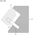
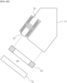
- FIGS. 4A and 4B illustrate the upper and lower plate structure of a first modified form of the temperature compensation module 20 according to an embodiment of the present disclosure.
- the first modified form of the temperature compensation module 20 is formed with a structure in which the second fixing part 23 extends from the basic form of the base and two ends of the moving member 25 are fixed and attached to the integrally formed upper base plate 41.
- the upper base plate 41 may be attached on or below the AWG, and the lower base plate 42 may be attached to a surface opposite the upper base plate 41 where the AWG is attached.
- One end of the moving member 25 is fixed to the first fixing part 22, and the other end is fixed to the lower base plate 42.
- the lower base plate 42 may further include a guide hole 43 to guide the horizontal movement of the moving member 25.
- the thickness of the lower base plate 42 may be larger than the thickness of the moving member 25, and the two ends of the moving member 25 may be fixed to the upper base plate 41 and the lower base plate 42 respectively to prevent the contact with the ground in the guide hole 43.
- the upper and lower base plates may be integrally formed as shown in FIGS. 4A and 4B .
- FIG. 4C illustrates a variation of the first modified form of the temperature compensation module 20 including the upper base plate 41 alone.
- the moving member 25 may be directly fixed to the upper base plate 41 without separately fabricating a lower base plate of a different shape from the upper base plate 41.
- the moving member 25 may be mounted in a first position 1 where the two ends of the moving member 25 are fixed to the first fixing part 22 and the upper base plate 41 parallel to the first fixing part 22 respectively, or a second position 2 where the two ends of the moving member 25 are fixed to an extension 44 of the first fixing part 22 and an extension 45 at the lower end of the upper base plate 41 respectively.
- FIGS. 4D to 4F illustrate other variations of the first modified form of the temperature compensation module 20 including the upper base plate 41 alone.
- the moving member 25 is directly fixed to the upper base plate 41 without separately fabricating a lower base plate of a different shape from the upper base plate 41.
- the first fixing part 22 and the upper base plate 41 may be machined with a structure for mounting the moving member 25 such that the two ends of the moving member 25 may be fixed and mounted in a recessed area of the first fixing part 22 and a recessed area at the lower end of the upper base plate 41 respectively.
- the moving member 25 may be formed with a structure in which the moving member 25 is fixed with screws at two ends, or the moving member 25 itself may be fabricated in the shape of a large screw.
- the moving member 25 may be fixed to the base in a simple manner by tightening the screw, and the chip may be aligned to a desired location.
- the first fixing part 22 and the upper base plate 41 may be fabricated in a linear shape as conventional without separately machining adhesion regions for the moving member 25.
- the two ends of the moving member 25 may be fixed and mounted to the end of the first fixing part 22 and the lower end of the upper base plate 41 parallel thereto, respectively.
- the moving member 25 may be a moving member 25 that is made of only a thermal compensation material and is attached, or a moving member 25' with attaching parts of different materials connected to the two ends of the thermal compensation material.
- the attaching parts of different materials at the two ends of the thermal compensation material may be the same material as the first fixing part 22 and the upper base plate 41, and may be made of metal, plastic, silicon or silica-based materials.
- the first fixing part 22 and the upper base plate 41 may be fabricated in a linear shape as conventional without separately machining adhesion regions for the moving member 25, but the moving member 25 may have a different shape.
- the moving member 25 may include a first attaching part 25-1 connected to one end of the thermal compensation material for attaching with the first fixing part 22, and a second attaching part 25-2 at the other end of the thermal compensation material for attaching to the upper base plate 41.
- the second attaching part may be extended to reduce the adhesion gap with the first attaching part 25-1.
- the width of the upper base plate 41 may be reduced by adjusting the distance between the first attaching part 25-1 and the second attaching part 25-2 rather than forming the attaching parts at the two ends of the thermal compensation material. Through this, it is possible to fabricate the temperature compensation module 20 with economic efficiency.
- the first attaching part 25-1 and the second attaching part 25-2 may be the same material as the first fixing part 22 and the upper base plate 41, and may be made of metal, plastic, silicon or silica-based materials.
- the first modified form of the temperature compensation module 20 is an extension integrated form, and it may be fabricated by simply cutting the planar substrate and may be a plate-type horizontal movement module that is easy to machine in order to change the shape.
- the base of the temperature compensation module 20 may be fabricated in a sufficient size to receive the entire AWG substrate, and through this, it is possible to assist the alignment and horizontal movement of the AWG substrate more precisely.
- FIG. 5 illustrates the structure of a second modified form of the temperature compensation module 20 according to an embodiment of the present disclosure.
- the second modified form of the temperature compensation module 20 includes an upper base plate 41' that is the same as the basic form of the base, and a lower base plate 42' that is fixed and attached to one surface of the second fixing part 23.
- the upper base plate 41' may be attached on or below the AWG
- the lower base plate 42' may be attached to a surface opposite the second fixing part 23 of the upper base plate 41' where the AWG is attached.
- One end of the moving member 25 is fixed to the first fixing part 22, and the other end is fixed to the lower base plate 42'.
- the upper and lower base plates may be integrally formed as shown in FIG. 5 .
- FIGS. 6A to 6C illustrate the top and side structure of the temperature compensation module 20 according to an embodiment of the present disclosure.
- the base 21 may further include a slit 51 and a dam 52 structure on the upper surface to assist the attachment of the AWG substrate.
- the first fixing part 22 and the second fixing part 23 of the base 21 may be fixed and attached to the first sub chip 10a including the input waveguide 1 of the AWG and the second sub chip 10b including the slab waveguide 2 respectively, and in this instance, a variety of fixing methods may be used.
- a liquid adhesive material such as epoxy
- the slit 51 and the dam 52 structure may be included on the upper surface of the base 21 to prevent the liquid adhesive material from flowing.
- the present disclosure does not necessarily include the slit 51 and the dam 52 structure, and the same goal may be achieved by precisely applying the adhesive material.
- a slit 53 structure may be included on the lower surface of the base 21, and the lower base plate 42, 42' structure may be attached to prevent the liquid adhesive material from flowing.
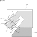
- FIGS. 7A to 7C illustrate examples of the AWGs with the temperature compensation modules 20 of various structures according to an embodiment of the present disclosure.
- the AWG with the basic form of the temperature compensation module 20 is shown.
- the first fixing part 22 of the base 21 is fixed to the first sub chip 10a of the AWG, and the second fixing part 23 is fixed to the second sub chip 10b of the AWG.
- the cutting plane 6 of the AWG for cutting into the two parts 10a, 10b is disposed in the hole 31 of the base 21 so that the first sub chip 10a is horizontally moved along the cutting plane 6 by the moving member 25 made of the thermal compensation material.
- the AWG with the basic form of the temperature compensation module 20 compensates for changes in the center wavelength with the changes in temperature, thereby achieving the athermal AWG.
- the AWG with the first modified form of the temperature compensation module 20 is shown.
- the first fixing part 22 of the upper base plate 41 is fixed to the first sub chip 10a of the AWG, and the second fixing part 23 is fixed to the second sub chip 10b of the AWG.
- the cutting plane 6 of the AWG for cutting into the two parts 10a, 10b is disposed in the hole 31 of the upper base plate 41 so that the first sub chip 10a is horizontally moved along the cutting plane 6 by the moving member 25 made of the thermal compensation material.
- the moving member 25 may be disposed in the guide hole 43 to achieve linear expansion/contraction without interruption.
- the AWG with the second modified form of the temperature compensation module 20 is shown.
- the first fixing part 22 of the upper base plate 41' is fixed to the first sub chip 10a of the AWG
- the second fixing part 23 is fixed to the second sub chip 10b of the AWG.
- the cutting plane 6 of the AWG for cutting into the two parts 10a, 10b is disposed in the hole 31 of the upper base plate 41' so that the first sub chip 10a is horizontally moved along the cutting plane 6 by the moving member 25 made of the thermal compensation material.
- the temperature compensation module 20 of FIGS. 7A to 7C is an extension integrated form, and it may be fabricated by simply cutting the planar substrate and may be a plate-type horizontal movement module that is easy to machine in order to change the shape.
- the base of the temperature compensation module 20 may be fabricated in a sufficient size to receive the entire AWG substrate, and through this, it is possible to assist the alignment and horizontal movement of the AWG substrate more precisely.
- the moving member 25 may be formed with a structure in which the moving member 25 is fixed with screws at two ends, or the moving member 25 itself may be fabricated in the shape of a large screw. Through the screw shape of the moving member 25, the moving member 25 may be fixed to the base in a simple manner, and the chip may be aligned to a desired location by adjusting the screw.
Landscapes
- Physics & Mathematics (AREA)
- Engineering & Computer Science (AREA)
- Microelectronics & Electronic Packaging (AREA)
- General Physics & Mathematics (AREA)
- Optics & Photonics (AREA)
- Optical Integrated Circuits (AREA)
Description
- The present disclosure relates to athermal arrayed waveguide grating (AWG) using a precise parallel movement module and a manufacturing method therefor, and more particularly, to athermal arrayed waveguide grating (AWG) with a temperature compensation module capable of precise horizontal movement to uniformly maintain the wavelength irrespective of outside temperature changes and a manufacturing method therefor.
- Recently, with the dramatic increase in different types of data services including the Internet, transmission capacity expansion of the backbone network is required. To meet the demand, one of solutions is to increase the transmission capacity of optical fibers through wavelength division multiplexing (WDM) optical communication systems that receive and transmit multiple channels of information through a single optical fiber.
- In the WDM, planar lightwave circuits (PLCs) having optical waveguides on a plate of silica by a combination of optical fiber technology and large scale integration (LSI) technology are used as wavelength division multiplexers/demultiplexers. The PLC (e.g., arrayed waveguide gratings (AWGs), splitters) changes in refractive index n with the changes in temperature T, and in the case of AWGs for wavelength division, the changes in refractive index n lead to changes in the path L of light that determines the wavelength, and changes in wavelength λ occur in the channel of each output port. Hereinafter, a general AWG will be described with reference to
FIG. 1 . -
FIG. 1 illustrates the structure of the general AWG. As shown inFIG. 1 , the AWG includes an input waveguide 1, aninput slab waveguide 2, anarray waveguide 3, an output slab waveguide 4 and anoutput waveguide 5. Actually, there is one input waveguide 1 defining an optical path, but at least one input waveguide 1 may be included to monitor the performance in the fabrication process. An optical signal inputted to the input waveguide 1 is split at each wavelength λ1, λ2, ..., λn and outputted to theoutput waveguide 5. That is, when wavelength λ1 is allocated to #1 channel, it is necessary that the wavelength λ1 is outputted to theoutput waveguide 5 despite changes in the surrounding environment. However, the refractive index changes with temperature, and as the refractive index changes, the wavelength of the AWG changes as well. Although the wavelength λ1 is allocated to #1 channel, as the temperature changes, an error may occur, for example, wavelength λ2 may be outputted. - In the use of the AWG as a wavelength division multiplexer, to prevent the error caused by the temperature change, packaging has been used to maintain uniform temperature at high temperature above the operating temperature using a precision heater. However, due to the problems with power consumption, outdoor power supply and high temperature-induced product's short life, studies have been made on athermal AWG structures for uniformly maintaining the wavelength irrespective of the temperature of the AWG itself.
- Referring to
FIG. 1 , acutting plane 6 for dividing a substrate into twoparts FIG. 1 compensates for wavelength with the changes in temperature to prevent the changes in wavelength at the output port by allowing thefirst sub chip 10a including the input waveguide 1 to move along thecutting plane 6. To move the position of the input waveguide 1 cut in a straight line, a material having the coefficient of thermal expansion that matches the change in wavelength is machined and used, and such a material is referred to as a temperature compensation material or a thermal compensation material and primarily includes metals having a high coefficient of thermal expansion. - The PLC that is one of optical communication components requires very precise alignment with the alignment tolerance of 0.5micrometers. Re-aligning the
first sub chip 10a and thesecond sub chip 10b of the AWG cut to achieve temperature insensitivity within the tolerance causes a challenging technical problem. -
KR 2006 0025984 A -
US 2008/135169 A1 discloses a method to compensate temperature dependency of center wavelength by adjusting optical input position passively by cutting the interface between the input slap waveguide of AWG and the stripe waveguide circuit connected to the input slab on a AWG chip, followed by attaching the lateral sliding rod which has the larger CTE (Coefficient of Thermal Expansion) than AWG chip substrate. -
US 2002/181871 A1 discloses an arrayed waveguide grating, in which at least one of two slab waveguides constituting the arrayed waveguide grating is cut and separated together with a substrate on a cross separating face, a slide moving member is arranged over a waveguide forming area formed on the substrate including the separating slab waveguide and a waveguide forming area formed on the substrate including the separating slab waveguide. -
CN 106 154 411 A discloses an athermal arrayed wavelength grating with a temperature compensation function and a manufacturing method thereof. The athermal arrayed wavelength grating comprises a base plate, an arrayed wavelength grating chip and a temperature compensation component, wherein the base plate comprises a first base plate part and a second base plate part; the temperature compensation component enables the first base plate part and the second base plate part which form the base plate to relatively move in parallel in a plane where the base plate is located; the arrayed wavelength grating chip is cut into a first chip part and a second chip part which move relative to each other; the first chip part and the second chip part are respectively fixed on the first base plate part and the second base plate part. - The present invention as defined by claim 1 is directed to a temperature compensation module mounted in an arrayed waveguide grating (AWG) in which a cutting plane is aligned within the tolerance using the temperature compensation module capable of precise horizontal movement to facilitate the alignment of the cutting plane of the athermal AWG and a manufacturing method of an athermal AWG using the temperature compensation module as defined by claim 11.
- The invention is set out in the appended set of claims.
- The present disclosure provides athermal arrayed waveguide grating (AWG) that facilitates the alignment of the cutting plane of the AWG and achieves precise horizontal movement without a change in vertical gap and difference of the cutting plane through the temperature compensation module capable of precise horizontal movement. Through this, it is possible to easily apply the thermal compensation material to both the upper and lower ends in motion, and uniformly maintain the center wavelength of the AWG device irrespective of temperature changes. Additionally, it is possible to simplify the fabrication process by simply attaching one modularized temperature compensation module to the chip, and ultimately, increase the reliability and productivity of products.
- The effects that can be obtained from the present disclosure are not limited to the above-mentioned effects, and other effects not mentioned herein will be clearly understood by those having ordinary skill in the art from the following description.
-
-
FIG. 1 illustrates a general arrayed waveguide grating (AWG) structure according to an embodiment of the present disclosure. -
FIG. 2 illustrates the basic structure of a temperature compensation module according to an embodiment of the present disclosure. -
FIG. 3 illustrates the alignment of a temperature compensation module and AWG according to an embodiment of the present disclosure. -
FIGS. 4A to 4F illustrate the structure of a first modified form of a temperature compensation module according to an embodiment of the present disclosure. -
FIG. 5 illustrates the structure of a second modified form of a temperature compensation module according to an embodiment of the present disclosure. -
FIGS. 6A to 6C illustrate the top and side structure of a temperature compensation module according to an embodiment of the present disclosure. -
FIGS. 7A to 7C illustrate examples of AWGs with temperature compensation modules of various structures according to an embodiment of the present disclosure. - These and other advantages and features of the present disclosure and methods for achieving them will be apparent by referring to the embodiments described in detail below together with the accompanying drawings. However, the present disclosure is not limited to the following disclosed embodiments and will be embodied in many different forms, and these embodiments are only provided to make the disclosure complete and help those having ordinary skill in the technical field pertaining to the present disclosure to understand the scope of the invention fully, and the present disclosure is only defined by the scope of the appended claims.
- The shape, size, proportion, angle and number shown in the drawings to describe the embodiments of the present disclosure are provided by way of illustration, and the present disclosure is not limited thereto. Additionally, in describing the present disclosure, when it is deemed that a certain detailed description of well-known related technology renders the key subject matter of the present disclosure unnecessarily ambiguous, the detailed description is omitted herein. The term 'comprises' or 'includes' as used herein does not preclude the presence or addition of other components unless 'only' is used. The singular forms as used herein include the plural forms as well unless the context clearly indicates otherwise.
- In interpreting the components, unless the context clearly indicates otherwise, it is interpreted that an error range is included.
- In the description of the positional relationship, for example, when the positional relationship of two components is described using 'on', 'above', 'below', 'next to', unless 'immediately' or 'directly' is used, at least one intervening component may be present.
- When an element or layer is referred to as being "on" another element or layer, the element or layer may be immediately on another element or layer, or intervening element(s) or layer(s) may be present. Like reference symbols indicate like components throughout the specification.
- The terms "first", "second", and the like are used to describe various components, but it is obvious that these components are not limited by the terms. These terms are used to distinguish one component from another. Accordingly, it is obvious that a first component as used herein may be a second component.
- The size and thickness of each component in the drawings is shown for convenience of description, and the present disclosure is not necessarily limited to the size and thickness of the components shown in the drawings.
- Each feature of the embodiments of the present disclosure may be united or combined together in part or in whole, and as sufficiently understood by those having ordinary skill in the art, a variety of technical connection and cooperation are possible, and each embodiment may be carried out independently of each other or in conjunction with each other.
- The athermal AWG is cut between an input waveguide 1 and an
input slab waveguide 2 or into theinput slab waveguide 2 to compensate for changes in the center wavelength by changing the location of incoming light with the changes in temperature. To this end, the structure of a temperature compensation module for easy alignment of the cutting plane of the athermal AWG and precise horizontal movement with the expansion/contraction of a thermal compensation material is shown inFIGS. 2 to 5 below. -
FIG. 2 illustrates the basic structure of thetemperature compensation module 20 according to an embodiment of the present disclosure. - Referring to
FIG. 2 , the basic structure of thetemperature compensation module 20 according to an embodiment of the present disclosure includes abase 21 and a movingmember 25. - The
base 21 is attached to an AWG substrate to facilitate the alignment between the cut parts of the AWG and assist the precise horizontal movement of the cut part of the AWG with the expansion and contraction of the movingmember 25 attached to a portion of thebase 21. To this end, thebase 21 includes a first fixingpart 22, a second fixingpart 23 and anelastic part 24 connecting the first fixingpart 22 and the second fixingpart 23. According to an embodiment of the present disclosure, preferably, thebase 21 may be integrally formed by machining such that thebase 21 includes the first fixingpart 22, the second fixingpart 23 and theelastic part 24 from one raw material, and is easy to machine in order to change the shape. When thebase 21 is made of a material having a large difference in coefficient of thermal expansion from the movingmember 25 of the thermal compensation material, it is possible to maximize the temperature compensation effect. For example, in general, the movingmember 25 uses a metal having a high coefficient of thermal expansion. The base 21 may be made of, for example, metal, plastic, silicon and silica-based materials having a lower coefficient of thermal expansion. According to an embodiment of the present disclosure, thebase 21 may be made of the same material as the AWG substrate. Through this, it is possible to prevent twists due to different coefficients of thermal expansion when thebase 21 and the AWG substrate are attached. - The first fixing
part 22 and the second fixingpart 23 may be fixed and attached to the AWG. For example, an adhesive such as epoxy may be used to fix and attach the first fixingpart 22 and the second fixingpart 23 to the AWG chip, but fixing is not necessarily conducted only by the adhesive. Various types of members may be used to fix and attach the first fixingpart 22 and the second fixingpart 23 to the AWG chip. According to an embodiment of the present disclosure, the movingmember 25 is attached to the first fixingpart 22 to cause linear movements of the separated part of the AWG through expansion/contraction with temperature, and through this, to compensate for changes in the optical properties with temperature. - The
elastic part 24 is formed with elasticity such that theelastic part 24 deforms to make linear movements as the movingmember 25 expands/contracts, but restores to the original shape. For example, theelastic part 24 is in the shape of a leaf spring, and includes asupport 26 machined in a very small thickness and aleg 27 connecting two ends of thesupport 26 to the first fixingpart 22 and the second fixingpart 23 respectively. Thesupport 26 and the horizontal portion of theleg 27 parallel to thesupport 26 may be machined in a very small thickness such that they have the width of a few mm or less according to the required elasticity.FIG. 2 only shows a structure in which theleg 27 connects the fixingparts support 26 at a right angle in the shape of '', but this is provided by way of illustration, any shape that assists the linear movement of the fixing part with elasticity is possible. For example, the upper and lower plates (the first and second fixing parts) with the ' ' shaped
elastic part 24 connected on the left and right sides in a symmetrical structure achieve precise horizontal movements due to offset of two circular movements. At the same time, theelastic part 24 of vertically thick structure suppresses vertical movements, so there is almost no change in vertical difference when the upper and lower plates make horizontal movements. That is, theelastic part 24 may be about a few mm in thickness, thereby suppressing vertical movements. -
FIG. 3 illustrates the alignment of thetemperature compensation module 20 and the AWG according to an embodiment of the present disclosure. - Referring to
FIG. 3 , when thebase 21 of thetemperature compensation module 20 is fixed and attached to the AWG, the first fixingpart 22 is attached to thefirst sub chip 10a, and the second fixingpart 23 is attached to thesecond sub chip 10b. For example, an adhesive such as epoxy may be used to fix and attach the first fixingpart 22 and the second fixingpart 23 to the AWG chip, but fixing is not necessarily conducted only by the adhesive. In this instance, thebase 21 of thetemperature compensation module 20 may be attached on or below the AWG. The cuttingplane 6 of the AWG may be formed by cutting between the input waveguide 1 and theinput slab waveguide 2, or may be formed inside theinput slab waveguide 2, and accordingly, thefirst sub chip 10a of the AWG includes the input waveguide 1, and thesecond sub chip 10b includes theinput slab waveguide 2. - The
base 21 of thetemperature compensation module 20 includes ahole 31 between the first fixingpart 22 and the second fixingpart 23 to allow the first fixingpart 22 and the second fixingpart 23 to move separately from each other. According to an embodiment of the present disclosure, thetemperature compensation module 20 and the AWG are placed in alignment such that the cuttingplane 6 of the AWG is included in thehole 31 to allow thefirst sub chip 10a to move separately from thesecond sub chip 10b. The base 21 may be integrally formed by machining from one raw material, and for this reason, may be a structure in which the height of thefirst sub chip 10a, i.e., a region including the input waveguide 1 accurately matches the height of thesecond sub chip 10b, i.e., a region including theinput slab waveguide 2. - For example, as shown in
FIG. 3 , when the center line of thehole 31 and the cuttingplane 6 of the AWG are placed in alignment, and the first fixingpart 22 is fixed to thefirst sub chip 10a and the second fixingpart 23 is fixed to thesecond sub chip 10b, thefirst sub chip 10a fixed to the first fixingpart 22 horizontally moves with the expansion/contraction of the movingmember 25 attached to the first fixingpart 22. In this instance, the horizontal movements are assisted by theelastic part 24, and it is possible to manufacture the athermal AWG that can move within the alignment tolerance (for example, 0.0005 mm). For example, the first and second fixing partswith the '' shaped
elastic part 24 connected on the left and right sides in a symmetrical structure achieve precise horizontal movements due to offset of two circular movements. Additionally, theelastic part 24 of vertically thick structure (for example, a few mm) suppresses vertical movements, so it is possible to achieve precise horizontal movements with almost no change in vertical difference when the upper and lower plates make horizontal movements. - According to an embodiment of the present disclosure, the step of cutting the AWG into the
first sub chip 10a and thesecond sub chip 10b in the process of manufacturing the athermal AWG may be performed before attaching thetemperature compensation module 20 to the AWG. However, the manufacturing process is not necessarily performed in such an order, and the athermal AWG may be manufactured in a simple manner by attaching thetemperature compensation module 20 to the AWG and cutting the AWG such that the cuttingplane 6 is disposed in the hole of thetemperature compensation module 20. -
FIGS. 4A and4B illustrate the upper and lower plate structure of a first modified form of thetemperature compensation module 20 according to an embodiment of the present disclosure. - Referring to
FIGS. 4A and4B , the first modified form of thetemperature compensation module 20 is formed with a structure in which the second fixingpart 23 extends from the basic form of the base and two ends of the movingmember 25 are fixed and attached to the integrally formedupper base plate 41. According to an embodiment of the present disclosure, theupper base plate 41 may be attached on or below the AWG, and thelower base plate 42 may be attached to a surface opposite theupper base plate 41 where the AWG is attached. One end of the movingmember 25 is fixed to the first fixingpart 22, and the other end is fixed to thelower base plate 42. Thelower base plate 42 may further include aguide hole 43 to guide the horizontal movement of the movingmember 25. Even though thelower base plate 42 is placed in contact with the ground, to prevent the expansion/contraction of the movingmember 25 from being interrupted, the thickness of thelower base plate 42 may be larger than the thickness of the movingmember 25, and the two ends of the movingmember 25 may be fixed to theupper base plate 41 and thelower base plate 42 respectively to prevent the contact with the ground in theguide hole 43. According to another embodiment, the upper and lower base plates may be integrally formed as shown inFIGS. 4A and4B . - According to various embodiments of the present disclosure,
FIG. 4C illustrates a variation of the first modified form of thetemperature compensation module 20 including theupper base plate 41 alone. Referring toFIG. 4C , the movingmember 25 may be directly fixed to theupper base plate 41 without separately fabricating a lower base plate of a different shape from theupper base plate 41. The movingmember 25 may be mounted in a first position ① where the two ends of the movingmember 25 are fixed to the first fixingpart 22 and theupper base plate 41 parallel to the first fixingpart 22 respectively, or asecond position ② where the two ends of the movingmember 25 are fixed to anextension 44 of the first fixingpart 22 and anextension 45 at the lower end of theupper base plate 41 respectively. - According to various embodiments of the present disclosure,
FIGS. 4D to 4F illustrate other variations of the first modified form of thetemperature compensation module 20 including theupper base plate 41 alone. - Referring to
FIG. 4D , the movingmember 25 is directly fixed to theupper base plate 41 without separately fabricating a lower base plate of a different shape from theupper base plate 41. Particularly, the first fixingpart 22 and theupper base plate 41 may be machined with a structure for mounting the movingmember 25 such that the two ends of the movingmember 25 may be fixed and mounted in a recessed area of the first fixingpart 22 and a recessed area at the lower end of theupper base plate 41 respectively. For example, the movingmember 25 may be formed with a structure in which the movingmember 25 is fixed with screws at two ends, or the movingmember 25 itself may be fabricated in the shape of a large screw. The movingmember 25 may be fixed to the base in a simple manner by tightening the screw, and the chip may be aligned to a desired location. - Referring to
FIG. 4E , as shown inFIG. 4D , the first fixingpart 22 and theupper base plate 41 may be fabricated in a linear shape as conventional without separately machining adhesion regions for the movingmember 25. The two ends of the movingmember 25 may be fixed and mounted to the end of the first fixingpart 22 and the lower end of theupper base plate 41 parallel thereto, respectively. In this instance, the movingmember 25 may be a movingmember 25 that is made of only a thermal compensation material and is attached, or a moving member 25' with attaching parts of different materials connected to the two ends of the thermal compensation material. The attaching parts of different materials at the two ends of the thermal compensation material may be the same material as the first fixingpart 22 and theupper base plate 41, and may be made of metal, plastic, silicon or silica-based materials. - Referring to
FIG. 4F , as shown inFIG. 4E , the first fixingpart 22 and theupper base plate 41 may be fabricated in a linear shape as conventional without separately machining adhesion regions for the movingmember 25, but the movingmember 25 may have a different shape. In this instance, the movingmember 25 may include a first attaching part 25-1 connected to one end of the thermal compensation material for attaching with the first fixingpart 22, and a second attaching part 25-2 at the other end of the thermal compensation material for attaching to theupper base plate 41. As shown inFIG. 4F , the second attaching part may be extended to reduce the adhesion gap with the first attaching part 25-1. Due to the required minimum length for the thermal compensation material, the width of theupper base plate 41 may be reduced by adjusting the distance between the first attaching part 25-1 and the second attaching part 25-2 rather than forming the attaching parts at the two ends of the thermal compensation material. Through this, it is possible to fabricate thetemperature compensation module 20 with economic efficiency. The first attaching part 25-1 and the second attaching part 25-2 may be the same material as the first fixingpart 22 and theupper base plate 41, and may be made of metal, plastic, silicon or silica-based materials. - For example, the first modified form of the
temperature compensation module 20 is an extension integrated form, and it may be fabricated by simply cutting the planar substrate and may be a plate-type horizontal movement module that is easy to machine in order to change the shape. According to an embodiment, the base of thetemperature compensation module 20 may be fabricated in a sufficient size to receive the entire AWG substrate, and through this, it is possible to assist the alignment and horizontal movement of the AWG substrate more precisely. -
FIG. 5 illustrates the structure of a second modified form of thetemperature compensation module 20 according to an embodiment of the present disclosure. - Referring to
FIG. 5 , the second modified form of thetemperature compensation module 20 includes an upper base plate 41' that is the same as the basic form of the base, and a lower base plate 42' that is fixed and attached to one surface of the second fixingpart 23. According to an embodiment of the present disclosure, the upper base plate 41' may be attached on or below the AWG, and the lower base plate 42' may be attached to a surface opposite the second fixingpart 23 of the upper base plate 41' where the AWG is attached. One end of the movingmember 25 is fixed to the first fixingpart 22, and the other end is fixed to the lower base plate 42'. According to another embodiment, the upper and lower base plates may be integrally formed as shown inFIG. 5 . -
FIGS. 6A to 6C illustrate the top and side structure of thetemperature compensation module 20 according to an embodiment of the present disclosure. - Referring to
FIG. 6A , thebase 21 may further include aslit 51 and adam 52 structure on the upper surface to assist the attachment of the AWG substrate. According to an embodiment of the present disclosure, the first fixingpart 22 and the second fixingpart 23 of the base 21 may be fixed and attached to thefirst sub chip 10a including the input waveguide 1 of the AWG and thesecond sub chip 10b including theslab waveguide 2 respectively, and in this instance, a variety of fixing methods may be used. For example, when a liquid adhesive material such as epoxy is used, it is necessary to prevent the liquid adhesive material from flowing in regions other than the first fixingpart 22 and the second fixingpart 23. It is to prevent the problem that theelastic part 24 cannot perform the intrinsic function when attached to the AWG. To this end, as shown inFIGS. 6A and6C , theslit 51 and thedam 52 structure may be included on the upper surface of the base 21 to prevent the liquid adhesive material from flowing. The present disclosure does not necessarily include theslit 51 and thedam 52 structure, and the same goal may be achieved by precisely applying the adhesive material. Referring toFIGS. 6B and 6C , aslit 53 structure may be included on the lower surface of thebase 21, and thelower base plate 42, 42' structure may be attached to prevent the liquid adhesive material from flowing. -
FIGS. 7A to 7C illustrate examples of the AWGs with thetemperature compensation modules 20 of various structures according to an embodiment of the present disclosure. - Referring to
FIG. 7A , the AWG with the basic form of thetemperature compensation module 20 is shown. The first fixingpart 22 of thebase 21 is fixed to thefirst sub chip 10a of the AWG, and the second fixingpart 23 is fixed to thesecond sub chip 10b of the AWG. The cuttingplane 6 of the AWG for cutting into the twoparts hole 31 of the base 21 so that thefirst sub chip 10a is horizontally moved along the cuttingplane 6 by the movingmember 25 made of the thermal compensation material. Through this, the AWG with the basic form of thetemperature compensation module 20 compensates for changes in the center wavelength with the changes in temperature, thereby achieving the athermal AWG. - Referring to
FIG. 7B , the AWG with the first modified form of thetemperature compensation module 20 is shown. The first fixingpart 22 of theupper base plate 41 is fixed to thefirst sub chip 10a of the AWG, and the second fixingpart 23 is fixed to thesecond sub chip 10b of the AWG. The cuttingplane 6 of the AWG for cutting into the twoparts hole 31 of theupper base plate 41 so that thefirst sub chip 10a is horizontally moved along the cuttingplane 6 by the movingmember 25 made of the thermal compensation material. As shown inFIG. 4B , the movingmember 25 may be disposed in theguide hole 43 to achieve linear expansion/contraction without interruption. - Referring to
FIG. 7C , the AWG with the second modified form of thetemperature compensation module 20 is shown. The first fixingpart 22 of the upper base plate 41' is fixed to thefirst sub chip 10a of the AWG, and the second fixingpart 23 is fixed to thesecond sub chip 10b of the AWG. The cuttingplane 6 of the AWG for cutting into the twoparts hole 31 of the upper base plate 41' so that thefirst sub chip 10a is horizontally moved along the cuttingplane 6 by the movingmember 25 made of the thermal compensation material. - According to an embodiment of the present disclosure, the
temperature compensation module 20 ofFIGS. 7A to 7C is an extension integrated form, and it may be fabricated by simply cutting the planar substrate and may be a plate-type horizontal movement module that is easy to machine in order to change the shape. According to an embodiment, the base of thetemperature compensation module 20 may be fabricated in a sufficient size to receive the entire AWG substrate, and through this, it is possible to assist the alignment and horizontal movement of the AWG substrate more precisely. In this instance, for example, the movingmember 25 may be formed with a structure in which the movingmember 25 is fixed with screws at two ends, or the movingmember 25 itself may be fabricated in the shape of a large screw. Through the screw shape of the movingmember 25, the movingmember 25 may be fixed to the base in a simple manner, and the chip may be aligned to a desired location by adjusting the screw. - In the specific embodiments described above, the components included in the present disclosure are represented in singular or plural forms according to the presented specific embodiments. However, the singular or plural forms are selected suitably for the presented context for convenience of description, and the above-described embodiments are not limited to the components in singular or plural forms, and the component represented in plural form may be singular and the component in singular form may be plural.
- While the specific embodiments have been described in the detailed description, various modifications may be made without departing from the scope of the appended claims. Therefore, the scope of the present disclosure should not be limited to the disclosed embodiments and should be defined by the appended claims.
Claims (15)
- A temperature compensation module (20) mounted in arrayed waveguide grating (AWG) to manually compensate for outside temperature changes, the temperature compensation module (20) comprising:a base (21) that is attached to the AWG; anda moving member (25) that is attached to the base (21),wherein the base (21) includes:a first fixing part (22) that is attached to a first sub chip (10a) including an input waveguide of the AWG;a second fixing part (23) that is attached to a second sub chip (10b) including an input slab waveguide of the AWG;a hole (31) being a gap between the first fixing part (22) and the second fixing part (23), the hole (31) disposed to include a cutting plane (6) within the gap, the cutting plane (6) for separating the AWG into the first sub chip (10a) and the second sub chip (10b); andan elastic part (24) to assist a linear movement of the first fixing part (22) and connect the first fixing part (22) and the second fixing part (23), characterized in,the elastic part (24) is in a shape of a leaf spring and includes a support (26) and a leg (27) connecting two ends of the support (26) to the first fixing part (22) and the second fixing part (23), respectively, and a horizontal portion of the leg (27) is parallel to the support (26), and a vertical structure of the elastic part (24) suppresses vertical movements, andthe moving member (25) is attached to the first fixing part (22) to horizontally move the first sub chip (10a) of the AWG along the cutting plane (6) by the moving member (25) made of a thermal compensation material, thereby arranged for reducing a change in center wavelength with a change in temperature.
- The temperature compensation module according to claim 1, wherein the base (21) is extended to a sufficient size to receive the entire AWG chip.
- The temperature compensation module according to claim 1 or 2, wherein each of the first fixing part (22) and the second fixing part (23) includes:a slit (51) being a protruding plane to apply an adhesive for fixing the AWG; anda dam (52) having a recessed shape to isolate the slit (51) to prevent the adhesive from flowing.
- The temperature compensation module according to claim 1 or 2, wherein the base includes:an upper base plate (41) that is attached to the AWG; anda lower base plate (42) formed on a surface opposite a surface of the upper base plate (41) where the AWG is attached, one end of the moving member (25) being attached to the lower base plate (42).
- The temperature compensation module according to claim 4, wherein the upper base plate (41) and the lower base plate (42) are integrally formed.
- The temperature compensation module according to claim 4, wherein the lower base plate (42) includes a guide hole (43) for guiding a linear movement of the moving member (25).
- The temperature compensation module according to claim 1 or 2, wherein the moving member (25) is made of a material having a higher coefficient of thermal expansion than the base, and
the base (21) is made of one of metal, plastic, silicon and silica-based materials having a lower coefficient of thermal expansion than the moving member (25). - An athermal arrayed waveguide grating (AWG) comprising a temperature compensation module of claim 1, the athermal arrayed waveguide grating comprising:an AWG planar substrate including an input waveguide (1), an input slab waveguide (2), an array waveguide (3), an output slab waveguide (4) and an output waveguide (5),wherein the temperature compensation module is mounted on or below the planar substrate.
- The athermal AWG according to claim 8, wherein the planar substrate is separated into a first sub chip (10a) including the input waveguide (1) and a second sub chip (10b) including the input slab waveguide (2) by a cutting plane (6) formed between the input waveguide (1) and the input slab waveguide (2) or inside the input slab waveguide (2).
- The athermal AWG according to claim 9, wherein the first fixing part (22) is attached to the first sub chip (10a), and the second fixing part (23) is attached to the second sub chip (10b), and
the moving member (25) is attached to the first fixing part (22) to allow the first sub chip (10a) to make a parallel movement along the cutting plane (6). - A method for manufacturing an athermal arrayed waveguide grating (AWG) as defined by claim 8, comprising:preparing an AWG planar substrate including an input waveguide (1), an input slab waveguide (2), an array waveguide (3), an output slab waveguide (4) and an output waveguide (5);placing the temperature compensation module (20) on or below the AWG; andattaching the temperature compensation module to the AWG.
- The method for manufacturing an athermal AWG according to claim 11, wherein placing the temperature compensation module (20) on or below the AWG comprises:
placing a cutting plane (6) within the hole (31), the cutting plane for separating the AWG into a first sub chip (10a) including the input waveguide (1) and a second sub chip (10b) including the input slab waveguide (2). - The method for manufacturing an athermal AWG according to claim 11, further comprising:
cutting between the input waveguide (1) and the input slab waveguide (2) or into the input slab waveguide (2) to separate the AWG into a first sub chip (10a) including the input waveguide (1) and a second sub chip (10b) including the input slab waveguide (2). - The method for manufacturing an athermal AWG according to claim 13, wherein attaching the temperature compensation module to the AWG comprises:
attaching the first fixing part (22) to the first sub chip (10a) and the second fixing part (23) to the second sub chip (10b). - The method for manufacturing an athermal AWG according to claim 13, wherein attaching the temperature compensation module (20) to the AWG comprises:applying an adhesive to a slit (51), wherein the slit (51) is a protruding plane from each of the first fixing part (22) and the second fixing part (23); andattaching the slit (51) of the first fixing part (22) to the first sub chip (10a) and the slit (51) of the second fixing part (23) to the second sub chip (10b),wherein each of the first fixing part (22) and the second fixing part (23) includes a dam (52) having a recessed shape to isolate the slit (51) to prevent the adhesive from flowing.
Applications Claiming Priority (2)
| Application Number | Priority Date | Filing Date | Title |
|---|---|---|---|
| KR1020180008858A KR101885498B1 (en) | 2018-01-24 | 2018-01-24 | Athermal arrayed waveguide grating using precision parallel movement module and manufacturing method thereof |
| PCT/KR2019/000648 WO2019146953A1 (en) | 2018-01-24 | 2019-01-16 | Athermal arrayed waveguide grating using precise parallel movement module, and manufacturing method therefor |
Publications (4)
| Publication Number | Publication Date |
|---|---|
| EP3745171A1 EP3745171A1 (en) | 2020-12-02 |
| EP3745171A4 EP3745171A4 (en) | 2021-12-08 |
| EP3745171B1 true EP3745171B1 (en) | 2025-04-23 |
| EP3745171C0 EP3745171C0 (en) | 2025-04-23 |
Family
ID=63250336
Family Applications (1)
| Application Number | Title | Priority Date | Filing Date |
|---|---|---|---|
| EP19743607.4A Active EP3745171B1 (en) | 2018-01-24 | 2019-01-16 | A temperature compensation module mounted in arrayed waveguide grating and a method of manufacturing an athermal arrayed waveguide grating |
Country Status (5)
| Country | Link |
|---|---|
| US (1) | US11092741B2 (en) |
| EP (1) | EP3745171B1 (en) |
| KR (1) | KR101885498B1 (en) |
| CN (1) | CN111630421B (en) |
| WO (1) | WO2019146953A1 (en) |
Families Citing this family (5)
| Publication number | Priority date | Publication date | Assignee | Title |
|---|---|---|---|---|
| CN109471219B (en) * | 2018-11-28 | 2020-06-30 | 武汉光迅科技股份有限公司 | AWG chip, manufacturing method and adjusting method thereof |
| CN113474703B (en) * | 2019-02-28 | 2023-10-20 | 莫列斯有限公司 | New and improved variable bidirectional thermal compensator for arrayed waveguide grating (AWG) modules |
| KR102952201B1 (en) * | 2020-07-31 | 2026-04-15 | 몰렉스 엘엘씨 | New and improved variable dual-directional thermal compensator for array waveguide grating (AWG) modules |
| JP7381174B2 (en) * | 2021-05-21 | 2023-11-15 | 三菱電機株式会社 | optical module |
| CN117092742A (en) * | 2022-05-11 | 2023-11-21 | 珠海保税区光联通讯技术有限公司 | Array waveguide grating device |
Family Cites Families (23)
| Publication number | Priority date | Publication date | Assignee | Title |
|---|---|---|---|---|
| JP2002071994A (en) * | 1999-12-27 | 2002-03-12 | Furukawa Electric Co Ltd:The | Array waveguide diffraction grating type optical multiplexer / demultiplexer and method of manufacturing the same |
| EP1148362A1 (en) * | 2000-04-20 | 2001-10-24 | JDS Uniphase Inc. | Arrayed waveguide grating having a reflective input coupling |
| JP3448551B2 (en) * | 2000-06-14 | 2003-09-22 | 古河電気工業株式会社 | Array waveguide type diffraction grating |
| EP1260837A4 (en) * | 2000-10-13 | 2005-11-09 | Furukawa Electric Co Ltd | Array waveguide type diffraction grating and light transmitting center wavelength correcting method |
| US6735364B2 (en) * | 2001-08-27 | 2004-05-11 | The Furukawa Electric Co., Ltd. | Arrayed waveguide grating optical multiplexer/demultiplexer and method for manufacturing the same |
| US6738545B1 (en) * | 2002-03-18 | 2004-05-18 | Lightwave Microsystems Corporation | Athermal AWG and AWG with low power consumption using groove of changeable width |
| US6954566B2 (en) * | 2002-07-25 | 2005-10-11 | Intel Corporation | Apparatus for thermal compensation of an arrayed waveguide grating |
| WO2005114288A1 (en) | 2004-05-05 | 2005-12-01 | Lightwave Microsystems Corporation | Athermal awg and awg with low power consumption using groove of changeable width |
| KR100795736B1 (en) * | 2004-11-03 | 2008-01-21 | 라이트웨이브 마이크로시스템스 코오포레이션 | Keep heatless and maintain low power consumption with variable grooves |
| KR100763790B1 (en) | 2005-01-07 | 2007-10-08 | (주)포인테크 | Temperature-independent optical waveguide grating and its manufacturing method |
| WO2008044838A1 (en) | 2006-10-10 | 2008-04-17 | Yun-Heum Park | Tiltable suspension |
| KR20060112697A (en) * | 2006-10-11 | 2006-11-01 | (주)포인테크 | Temperature-independent thermal grating waveguide module and its manufacturing method |
| CN100538414C (en) * | 2007-11-26 | 2009-09-09 | 武汉光迅科技股份有限公司 | Method and fine-tuning device for fabricating athermal arrayed waveguide grating based on slab waveguide movement |
| JP2010152177A (en) * | 2008-12-25 | 2010-07-08 | Furukawa Electric Co Ltd:The | Athermal awg module |
| WO2010099251A2 (en) * | 2009-02-26 | 2010-09-02 | Aidi Corporation | Arrayed waveguide grating (awg) with different radii in the input and output slab regions |
| JP2012014071A (en) * | 2010-07-02 | 2012-01-19 | Furukawa Electric Co Ltd:The | Array waveguide diffraction grating type optical multiplexer/demultiplexer |
| KR101338963B1 (en) | 2012-08-06 | 2013-12-09 | 주식회사 피피아이 | Athermal arrayed waveguide grating |
| CN103926654B (en) * | 2014-04-25 | 2017-06-06 | 珠海保税区光联通讯技术有限公司 | Afebrile array waveguide grating wavelength division multiplexer |
| CN104090339B (en) * | 2014-07-03 | 2017-03-29 | 深圳市易飞扬通信技术有限公司 | Arrayed waveguide grating multiplexer |
| CN104280821B (en) * | 2014-10-31 | 2017-11-10 | 武汉光迅科技股份有限公司 | A kind of temperature insensitive arrayed waveguide grating (AAWG) of temperature section compensation |
| CN105866882B (en) * | 2016-05-31 | 2019-04-09 | 武汉光迅科技股份有限公司 | A temperature-insensitive arrayed waveguide grating with temperature compensation |
| CN106154411B (en) * | 2016-08-26 | 2019-08-13 | 武汉光迅科技股份有限公司 | An athermal arrayed waveguide grating with temperature compensation and its manufacturing method |
| CN206863273U (en) * | 2017-09-22 | 2018-01-09 | 武汉驿路通科技股份有限公司 | A kind of afebrile array waveguide grating wavelength division multiplexer |
-
2018
- 2018-01-24 KR KR1020180008858A patent/KR101885498B1/en active Active
-
2019
- 2019-01-16 EP EP19743607.4A patent/EP3745171B1/en active Active
- 2019-01-16 CN CN201980009220.1A patent/CN111630421B/en active Active
- 2019-01-16 WO PCT/KR2019/000648 patent/WO2019146953A1/en not_active Ceased
- 2019-01-16 US US16/964,310 patent/US11092741B2/en active Active
Also Published As
| Publication number | Publication date |
|---|---|
| WO2019146953A1 (en) | 2019-08-01 |
| EP3745171C0 (en) | 2025-04-23 |
| US20210041626A1 (en) | 2021-02-11 |
| EP3745171A1 (en) | 2020-12-02 |
| CN111630421A (en) | 2020-09-04 |
| US11092741B2 (en) | 2021-08-17 |
| EP3745171A4 (en) | 2021-12-08 |
| KR101885498B1 (en) | 2018-08-03 |
| CN111630421B (en) | 2023-04-04 |
Similar Documents
| Publication | Publication Date | Title |
|---|---|---|
| US11092741B2 (en) | Athermal arrayed waveguide grating using precise parallel movement module, and manufacturing method therefor | |
| US6738545B1 (en) | Athermal AWG and AWG with low power consumption using groove of changeable width | |
| US6954566B2 (en) | Apparatus for thermal compensation of an arrayed waveguide grating | |
| CA2320538C (en) | Arrayed waveguide grating and method for compensating optical transmitting center wavelength of light travelling through the same | |
| CN101419313B (en) | Fabrication method of athermal arrayed waveguide grating based on slab waveguide movement | |
| EP2074453B1 (en) | Stable center wavelength performance in non-rectilinearly shaped optical integrated circuit chip | |
| RU2596176C2 (en) | Temperature-compensated grating units based on set of waveguides | |
| JP4688869B2 (en) | Low power AWG using athermal AWG and variable width grooves | |
| CN102985858A (en) | Arrayed waveguide grating type optical multiplexer/demultiplexer | |
| WO2006073229A1 (en) | Packaging method of temperature insensitive arrayed waveguide grating | |
| JP5351522B2 (en) | Temperature-independent arrayed waveguide grating multiplexer / demultiplexer and its fabrication method for optical property compensation | |
| US6735364B2 (en) | Arrayed waveguide grating optical multiplexer/demultiplexer and method for manufacturing the same | |
| CN101414030B (en) | Temperature compensation rod and method for manufacturing multiplexing and de-multiplexing non-heat array wave guide grating | |
| CN101458364A (en) | Optimized making method based on flat-plate wave guide mobile afebrile array wave guide grating | |
| US20120195552A1 (en) | Arrayed waveguide grating type optical multiplexer and demultiplexer | |
| KR101885497B1 (en) | Arrayed waveguide grating with temperature compensation module suitable for uv curing assembly and method thereof | |
| JP5075048B2 (en) | Alignment method for arrayed waveguide grating and alignment device for arrayed waveguide grating | |
| KR20060112697A (en) | Temperature-independent thermal grating waveguide module and its manufacturing method | |
| KR100795736B1 (en) | Keep heatless and maintain low power consumption with variable grooves | |
| JP2010204696A (en) | Method of manufacturing array waveguide diffraction grating | |
| KR101341940B1 (en) | Athermal arrayed waveguide grating module | |
| HK1110396B (en) | Athermal awg and awg with low power consumption using groove of changeable width |
Legal Events
| Date | Code | Title | Description |
|---|---|---|---|
| STAA | Information on the status of an ep patent application or granted ep patent |
Free format text: STATUS: THE INTERNATIONAL PUBLICATION HAS BEEN MADE |
|
| PUAI | Public reference made under article 153(3) epc to a published international application that has entered the european phase |
Free format text: ORIGINAL CODE: 0009012 |
|
| STAA | Information on the status of an ep patent application or granted ep patent |
Free format text: STATUS: REQUEST FOR EXAMINATION WAS MADE |
|
| 17P | Request for examination filed |
Effective date: 20200728 |
|
| AK | Designated contracting states |
Kind code of ref document: A1 Designated state(s): AL AT BE BG CH CY CZ DE DK EE ES FI FR GB GR HR HU IE IS IT LI LT LU LV MC MK MT NL NO PL PT RO RS SE SI SK SM TR |
|
| AX | Request for extension of the european patent |
Extension state: BA ME |
|
| DAV | Request for validation of the european patent (deleted) | ||
| DAX | Request for extension of the european patent (deleted) | ||
| A4 | Supplementary search report drawn up and despatched |
Effective date: 20211105 |
|
| RIC1 | Information provided on ipc code assigned before grant |
Ipc: G02B 6/12 20060101AFI20211029BHEP |
|
| STAA | Information on the status of an ep patent application or granted ep patent |
Free format text: STATUS: EXAMINATION IS IN PROGRESS |
|
| 17Q | First examination report despatched |
Effective date: 20230329 |
|
| GRAP | Despatch of communication of intention to grant a patent |
Free format text: ORIGINAL CODE: EPIDOSNIGR1 |
|
| STAA | Information on the status of an ep patent application or granted ep patent |
Free format text: STATUS: GRANT OF PATENT IS INTENDED |
|
| INTG | Intention to grant announced |
Effective date: 20250117 |
|
| GRAS | Grant fee paid |
Free format text: ORIGINAL CODE: EPIDOSNIGR3 |
|
| GRAA | (expected) grant |
Free format text: ORIGINAL CODE: 0009210 |
|
| STAA | Information on the status of an ep patent application or granted ep patent |
Free format text: STATUS: THE PATENT HAS BEEN GRANTED |
|
| AK | Designated contracting states |
Kind code of ref document: B1 Designated state(s): AL AT BE BG CH CY CZ DE DK EE ES FI FR GB GR HR HU IE IS IT LI LT LU LV MC MK MT NL NO PL PT RO RS SE SI SK SM TR |
|
| REG | Reference to a national code |
Ref country code: GB Ref legal event code: FG4D |
|
| REG | Reference to a national code |
Ref country code: CH Ref legal event code: EP |
|
| REG | Reference to a national code |
Ref country code: DE Ref legal event code: R096 Ref document number: 602019068998 Country of ref document: DE |
|
| REG | Reference to a national code |
Ref country code: IE Ref legal event code: FG4D |
|
| U01 | Request for unitary effect filed |
Effective date: 20250424 |
|
| U07 | Unitary effect registered |
Designated state(s): AT BE BG DE DK EE FI FR IT LT LU LV MT NL PT RO SE SI Effective date: 20250430 |
|
| PG25 | Lapsed in a contracting state [announced via postgrant information from national office to epo] |
Ref country code: ES Free format text: LAPSE BECAUSE OF FAILURE TO SUBMIT A TRANSLATION OF THE DESCRIPTION OR TO PAY THE FEE WITHIN THE PRESCRIBED TIME-LIMIT Effective date: 20250423 |
|
| PG25 | Lapsed in a contracting state [announced via postgrant information from national office to epo] |
Ref country code: NO Free format text: LAPSE BECAUSE OF FAILURE TO SUBMIT A TRANSLATION OF THE DESCRIPTION OR TO PAY THE FEE WITHIN THE PRESCRIBED TIME-LIMIT Effective date: 20250723 Ref country code: GR Free format text: LAPSE BECAUSE OF FAILURE TO SUBMIT A TRANSLATION OF THE DESCRIPTION OR TO PAY THE FEE WITHIN THE PRESCRIBED TIME-LIMIT Effective date: 20250724 |
|
| PG25 | Lapsed in a contracting state [announced via postgrant information from national office to epo] |
Ref country code: PL Free format text: LAPSE BECAUSE OF FAILURE TO SUBMIT A TRANSLATION OF THE DESCRIPTION OR TO PAY THE FEE WITHIN THE PRESCRIBED TIME-LIMIT Effective date: 20250423 |
|
| PG25 | Lapsed in a contracting state [announced via postgrant information from national office to epo] |
Ref country code: HR Free format text: LAPSE BECAUSE OF FAILURE TO SUBMIT A TRANSLATION OF THE DESCRIPTION OR TO PAY THE FEE WITHIN THE PRESCRIBED TIME-LIMIT Effective date: 20250423 |
|
| PG25 | Lapsed in a contracting state [announced via postgrant information from national office to epo] |
Ref country code: RS Free format text: LAPSE BECAUSE OF FAILURE TO SUBMIT A TRANSLATION OF THE DESCRIPTION OR TO PAY THE FEE WITHIN THE PRESCRIBED TIME-LIMIT Effective date: 20250723 |
|
| PG25 | Lapsed in a contracting state [announced via postgrant information from national office to epo] |
Ref country code: IS Free format text: LAPSE BECAUSE OF FAILURE TO SUBMIT A TRANSLATION OF THE DESCRIPTION OR TO PAY THE FEE WITHIN THE PRESCRIBED TIME-LIMIT Effective date: 20250823 |
|
| PG25 | Lapsed in a contracting state [announced via postgrant information from national office to epo] |
Ref country code: SM Free format text: LAPSE BECAUSE OF FAILURE TO SUBMIT A TRANSLATION OF THE DESCRIPTION OR TO PAY THE FEE WITHIN THE PRESCRIBED TIME-LIMIT Effective date: 20250423 |
|
| PG25 | Lapsed in a contracting state [announced via postgrant information from national office to epo] |
Ref country code: CZ Free format text: LAPSE BECAUSE OF FAILURE TO SUBMIT A TRANSLATION OF THE DESCRIPTION OR TO PAY THE FEE WITHIN THE PRESCRIBED TIME-LIMIT Effective date: 20250423 |
|
| PG25 | Lapsed in a contracting state [announced via postgrant information from national office to epo] |
Ref country code: SK Free format text: LAPSE BECAUSE OF FAILURE TO SUBMIT A TRANSLATION OF THE DESCRIPTION OR TO PAY THE FEE WITHIN THE PRESCRIBED TIME-LIMIT Effective date: 20250423 |
|
| U20 | Renewal fee for the european patent with unitary effect paid |
Year of fee payment: 8 Effective date: 20260121 |
|
| PLBE | No opposition filed within time limit |
Free format text: ORIGINAL CODE: 0009261 |
|
| STAA | Information on the status of an ep patent application or granted ep patent |
Free format text: STATUS: NO OPPOSITION FILED WITHIN TIME LIMIT |
|
| REG | Reference to a national code |
Ref country code: CH Ref legal event code: L10 Free format text: ST27 STATUS EVENT CODE: U-0-0-L10-L00 (AS PROVIDED BY THE NATIONAL OFFICE) Effective date: 20260304 |
|
| 26N | No opposition filed |
Effective date: 20260126 |