EP3745113A1 - Inspection device, ptp packaging machine, and calibration method of inspection device - Google Patents
Inspection device, ptp packaging machine, and calibration method of inspection device Download PDFInfo
- Publication number
- EP3745113A1 EP3745113A1 EP18902271.8A EP18902271A EP3745113A1 EP 3745113 A1 EP3745113 A1 EP 3745113A1 EP 18902271 A EP18902271 A EP 18902271A EP 3745113 A1 EP3745113 A1 EP 3745113A1
- Authority
- EP
- European Patent Office
- Prior art keywords
- pixel
- image data
- inspection
- regard
- spectroscopic image
- Prior art date
- Legal status (The legal status is an assumption and is not a legal conclusion. Google has not performed a legal analysis and makes no representation as to the accuracy of the status listed.)
- Granted
Links
Images


Classifications
-
- B—PERFORMING OPERATIONS; TRANSPORTING
- B29—WORKING OF PLASTICS; WORKING OF SUBSTANCES IN A PLASTIC STATE IN GENERAL
- B29C—SHAPING OR JOINING OF PLASTICS; SHAPING OF MATERIAL IN A PLASTIC STATE, NOT OTHERWISE PROVIDED FOR; AFTER-TREATMENT OF THE SHAPED PRODUCTS, e.g. REPAIRING
- B29C51/00—Shaping by thermoforming, i.e. shaping sheets or sheet like preforms after heating, e.g. shaping sheets in matched moulds or by deep-drawing; Apparatus therefor
- B29C51/26—Component parts, details or accessories; Auxiliary operations
- B29C51/266—Auxiliary operations after the thermoforming operation
-
- G—PHYSICS
- G01—MEASURING; TESTING
- G01N—INVESTIGATING OR ANALYSING MATERIALS BY DETERMINING THEIR CHEMICAL OR PHYSICAL PROPERTIES
- G01N21/00—Investigating or analysing materials by the use of optical means, i.e. using sub-millimetre waves, infrared, visible or ultraviolet light
- G01N21/84—Systems specially adapted for particular applications
- G01N21/86—Investigating moving sheets
-
- B—PERFORMING OPERATIONS; TRANSPORTING
- B65—CONVEYING; PACKING; STORING; HANDLING THIN OR FILAMENTARY MATERIAL
- B65B—MACHINES, APPARATUS OR DEVICES FOR, OR METHODS OF, PACKAGING ARTICLES OR MATERIALS; UNPACKING
- B65B5/00—Packaging individual articles in containers or receptacles, e.g. bags, sacks, boxes, cartons, cans, jars
- B65B5/02—Machines characterised by incorporation of means for making the containers or receptacles
-
- B—PERFORMING OPERATIONS; TRANSPORTING
- B65—CONVEYING; PACKING; STORING; HANDLING THIN OR FILAMENTARY MATERIAL
- B65B—MACHINES, APPARATUS OR DEVICES FOR, OR METHODS OF, PACKAGING ARTICLES OR MATERIALS; UNPACKING
- B65B5/00—Packaging individual articles in containers or receptacles, e.g. bags, sacks, boxes, cartons, cans, jars
- B65B5/10—Filling containers or receptacles progressively or in stages by introducing successive articles, or layers of articles
- B65B5/101—Filling containers or receptacles progressively or in stages by introducing successive articles, or layers of articles by gravity
- B65B5/103—Filling containers or receptacles progressively or in stages by introducing successive articles, or layers of articles by gravity for packaging pills or tablets
-
- B—PERFORMING OPERATIONS; TRANSPORTING
- B65—CONVEYING; PACKING; STORING; HANDLING THIN OR FILAMENTARY MATERIAL
- B65B—MACHINES, APPARATUS OR DEVICES FOR, OR METHODS OF, PACKAGING ARTICLES OR MATERIALS; UNPACKING
- B65B57/00—Automatic control, checking, warning, or safety devices
-
- B—PERFORMING OPERATIONS; TRANSPORTING
- B65—CONVEYING; PACKING; STORING; HANDLING THIN OR FILAMENTARY MATERIAL
- B65B—MACHINES, APPARATUS OR DEVICES FOR, OR METHODS OF, PACKAGING ARTICLES OR MATERIALS; UNPACKING
- B65B57/00—Automatic control, checking, warning, or safety devices
- B65B57/10—Automatic control, checking, warning, or safety devices responsive to absence, presence, abnormal feed, or misplacement of articles or materials to be packaged
-
- G—PHYSICS
- G01—MEASURING; TESTING
- G01N—INVESTIGATING OR ANALYSING MATERIALS BY DETERMINING THEIR CHEMICAL OR PHYSICAL PROPERTIES
- G01N21/00—Investigating or analysing materials by the use of optical means, i.e. using sub-millimetre waves, infrared, visible or ultraviolet light
- G01N21/17—Systems in which incident light is modified in accordance with the properties of the material investigated
- G01N21/25—Colour; Spectral properties, i.e. comparison of effect of material on the light at two or more different wavelengths or wavelength bands
- G01N21/31—Investigating relative effect of material at wavelengths characteristic of specific elements or molecules, e.g. atomic absorption spectrometry
- G01N21/35—Investigating relative effect of material at wavelengths characteristic of specific elements or molecules, e.g. atomic absorption spectrometry using infrared light
- G01N21/3563—Investigating relative effect of material at wavelengths characteristic of specific elements or molecules, e.g. atomic absorption spectrometry using infrared light for analysing solids; Preparation of samples therefor
-
- G—PHYSICS
- G01—MEASURING; TESTING
- G01N—INVESTIGATING OR ANALYSING MATERIALS BY DETERMINING THEIR CHEMICAL OR PHYSICAL PROPERTIES
- G01N21/00—Investigating or analysing materials by the use of optical means, i.e. using sub-millimetre waves, infrared, visible or ultraviolet light
- G01N21/17—Systems in which incident light is modified in accordance with the properties of the material investigated
- G01N21/25—Colour; Spectral properties, i.e. comparison of effect of material on the light at two or more different wavelengths or wavelength bands
- G01N21/31—Investigating relative effect of material at wavelengths characteristic of specific elements or molecules, e.g. atomic absorption spectrometry
- G01N21/35—Investigating relative effect of material at wavelengths characteristic of specific elements or molecules, e.g. atomic absorption spectrometry using infrared light
- G01N21/359—Investigating relative effect of material at wavelengths characteristic of specific elements or molecules, e.g. atomic absorption spectrometry using infrared light using near infrared light
-
- G—PHYSICS
- G01—MEASURING; TESTING
- G01N—INVESTIGATING OR ANALYSING MATERIALS BY DETERMINING THEIR CHEMICAL OR PHYSICAL PROPERTIES
- G01N21/00—Investigating or analysing materials by the use of optical means, i.e. using sub-millimetre waves, infrared, visible or ultraviolet light
- G01N21/84—Systems specially adapted for particular applications
- G01N21/88—Investigating the presence of flaws or contamination
- G01N21/93—Detection standards; Calibrating baseline adjustment, drift correction
-
- G—PHYSICS
- G01—MEASURING; TESTING
- G01N—INVESTIGATING OR ANALYSING MATERIALS BY DETERMINING THEIR CHEMICAL OR PHYSICAL PROPERTIES
- G01N21/00—Investigating or analysing materials by the use of optical means, i.e. using sub-millimetre waves, infrared, visible or ultraviolet light
- G01N21/84—Systems specially adapted for particular applications
- G01N21/88—Investigating the presence of flaws or contamination
- G01N21/95—Investigating the presence of flaws or contamination characterised by the material or shape of the object to be examined
- G01N21/9508—Capsules; Tablets
-
- G—PHYSICS
- G06—COMPUTING OR CALCULATING; COUNTING
- G06T—IMAGE DATA PROCESSING OR GENERATION, IN GENERAL
- G06T7/00—Image analysis
- G06T7/0002—Inspection of images, e.g. flaw detection
- G06T7/0004—Industrial image inspection
-
- B—PERFORMING OPERATIONS; TRANSPORTING
- B29—WORKING OF PLASTICS; WORKING OF SUBSTANCES IN A PLASTIC STATE IN GENERAL
- B29C—SHAPING OR JOINING OF PLASTICS; SHAPING OF MATERIAL IN A PLASTIC STATE, NOT OTHERWISE PROVIDED FOR; AFTER-TREATMENT OF THE SHAPED PRODUCTS, e.g. REPAIRING
- B29C2793/00—Shaping techniques involving a cutting or machining operation
- B29C2793/0009—Cutting out
-
- B—PERFORMING OPERATIONS; TRANSPORTING
- B29—WORKING OF PLASTICS; WORKING OF SUBSTANCES IN A PLASTIC STATE IN GENERAL
- B29C—SHAPING OR JOINING OF PLASTICS; SHAPING OF MATERIAL IN A PLASTIC STATE, NOT OTHERWISE PROVIDED FOR; AFTER-TREATMENT OF THE SHAPED PRODUCTS, e.g. REPAIRING
- B29C2793/00—Shaping techniques involving a cutting or machining operation
- B29C2793/009—Shaping techniques involving a cutting or machining operation after shaping
-
- B—PERFORMING OPERATIONS; TRANSPORTING
- B29—WORKING OF PLASTICS; WORKING OF SUBSTANCES IN A PLASTIC STATE IN GENERAL
- B29C—SHAPING OR JOINING OF PLASTICS; SHAPING OF MATERIAL IN A PLASTIC STATE, NOT OTHERWISE PROVIDED FOR; AFTER-TREATMENT OF THE SHAPED PRODUCTS, e.g. REPAIRING
- B29C51/00—Shaping by thermoforming, i.e. shaping sheets or sheet like preforms after heating, e.g. shaping sheets in matched moulds or by deep-drawing; Apparatus therefor
- B29C51/18—Thermoforming apparatus
-
- B—PERFORMING OPERATIONS; TRANSPORTING
- B29—WORKING OF PLASTICS; WORKING OF SUBSTANCES IN A PLASTIC STATE IN GENERAL
- B29C—SHAPING OR JOINING OF PLASTICS; SHAPING OF MATERIAL IN A PLASTIC STATE, NOT OTHERWISE PROVIDED FOR; AFTER-TREATMENT OF THE SHAPED PRODUCTS, e.g. REPAIRING
- B29C51/00—Shaping by thermoforming, i.e. shaping sheets or sheet like preforms after heating, e.g. shaping sheets in matched moulds or by deep-drawing; Apparatus therefor
- B29C51/26—Component parts, details or accessories; Auxiliary operations
- B29C51/46—Measuring, controlling or regulating
-
- B—PERFORMING OPERATIONS; TRANSPORTING
- B29—WORKING OF PLASTICS; WORKING OF SUBSTANCES IN A PLASTIC STATE IN GENERAL
- B29L—INDEXING SCHEME ASSOCIATED WITH SUBCLASS B29C, RELATING TO PARTICULAR ARTICLES
- B29L2031/00—Other particular articles
- B29L2031/712—Containers; Packaging elements or accessories, Packages
-
- B—PERFORMING OPERATIONS; TRANSPORTING
- B65—CONVEYING; PACKING; STORING; HANDLING THIN OR FILAMENTARY MATERIAL
- B65B—MACHINES, APPARATUS OR DEVICES FOR, OR METHODS OF, PACKAGING ARTICLES OR MATERIALS; UNPACKING
- B65B9/00—Enclosing successive articles, or quantities of material, e.g. liquids or semiliquids, in flat, folded, or tubular webs of flexible sheet material; Subdividing filled flexible tubes to form packages
- B65B9/02—Enclosing successive articles, or quantities of material between opposed webs
- B65B9/04—Enclosing successive articles, or quantities of material between opposed webs one or both webs being formed with pockets for the reception of the articles, or of the quantities of material
- B65B9/045—Enclosing successive articles, or quantities of material between opposed webs one or both webs being formed with pockets for the reception of the articles, or of the quantities of material for single articles, e.g. tablets
-
- G—PHYSICS
- G01—MEASURING; TESTING
- G01N—INVESTIGATING OR ANALYSING MATERIALS BY DETERMINING THEIR CHEMICAL OR PHYSICAL PROPERTIES
- G01N21/00—Investigating or analysing materials by the use of optical means, i.e. using sub-millimetre waves, infrared, visible or ultraviolet light
- G01N21/84—Systems specially adapted for particular applications
- G01N21/86—Investigating moving sheets
- G01N2021/869—Plastics or polymeric material, e.g. polymers orientation in plastic, adhesive imprinted band
-
- G—PHYSICS
- G01—MEASURING; TESTING
- G01N—INVESTIGATING OR ANALYSING MATERIALS BY DETERMINING THEIR CHEMICAL OR PHYSICAL PROPERTIES
- G01N2201/00—Features of devices classified in G01N21/00
- G01N2201/12—Circuits of general importance; Signal processing
- G01N2201/127—Calibration; base line adjustment; drift compensation
Definitions
- the present disclosure relates to an inspection device configured to perform inspection for inclusion of any different type of object and the like by taking advantage of spectral analysis, a PTP packaging machine equipped with the inspection device, and a calibration method of the inspection device.
- a PTP sheet is generally comprised of a container film that has pocket portions filled with objects, such as tablets, and a cover film that is mounted to the container film such as to seal openings of the pocket portions.
- a different type inclusion inspection is performed to inspect for inclusion of any different type of object.
- a method that takes advantage of spectral analysis has conventionally been known as a technique for such inspection.
- this technique irradiates an object 83 filled in a pocket portion 82 of a container film 81 with near-infrared light L 1 emitted from a light source, such as a halogen lamp in the manufacturing process of the PTP sheet.
- a light source such as a halogen lamp in the manufacturing process of the PTP sheet.
- Reflected light L 2 that is reflected from the object 83 or the like is focused by an optical lens 85 to parallel light L 3 .
- Light passing through a slit 86 out of the parallel light L 3 forms slit light L 4 in a strip form and enters a spectroscope (prism) 87 serving as a spectroscopic unit.
- the slit light L 4 entering the spectroscope 87 is dispersed into lights of respective wavelength components, which are projected as an optical spectrum (optical spectral image) L 5 onto a light receiving surface 89 of an imaging element 88.
- optical spectrum optical spectral image
- near-infrared light in a wavelength band is dispersed into several ten to several hundred bands in a wavelength resolution of 1 nm to 10 nm intervals.
- the respective wavelength components of the optical spectrum L 5 are projected at different positions on the light receiving surface 89 of the imaging element 88 according to the difference of the wavelength components. Inclusion of a different type of object is detectable by principal component analysis of spectral data obtained by taking an image of this optical spectrum L5.
- a recently proposed configuration of an inspection device uses an imaging element such as a CCD area sensor to simultaneously inspect objects that are respectively filled in a plurality of pocket portions arranged in a line in a width direction of a container film conveyed (as described in, for example, Patent Literature 1).
- the imaging element such as the CCD area sensor is comprised of a plurality of light receiving elements arranged in a matrix arrangement. There is accordingly a need to correct a variation in the sensitivity based on the characteristics of the individual light receiving elements.
- a conventionally known method of correcting a variation in the sensitivity of the light receiving elements is, for example, a method that divides a luminance value of each pixel of image data obtained by taking an image of a standard plate irradiated with light of uniform intensity (uniform light) by an average luminance value of all pixels to calculate a sensitivity value at a coordinate position corresponding to the pixel and that divides a luminance value of each pixel of obtained inspection image data by the sensitivity value with regard to the pixel to correct the luminance value of the inspection image data in the process of inspection (as described in, for example, Background of Patent Literature 2).
- the intensities of the respective wavelength components included in the near-infrared light emitted from the light source such as the halogen lamp are, however, not uniform.
- the sensitivity of the imaging element is thus significantly changed by the respective wavelength components in the case of imaging the optical spectrum.
- an object of the present disclosure is to provide an inspection device configured to improve the inspection accuracy in an inspection that is performed by taking advantage of spectral analysis, as well as a PTP packaging machine and a calibration method of the inspection device.
- an inspection device comprising an irradiation unit configured to irradiate an object with near-infrared light; a spectral unit configured to disperse reflected light that is reflected from the object irradiated with the near-infrared light; and an imaging unit provided with an imaging element that includes a plurality of light-receiving elements arranged in a matrix arrangement and configured to take an image of an optical spectrum of the reflected light dispersed by the spectral unit.
- the inspection device is configured to perform a predetermined inspection (for example, different type inclusion inspection) by taking advantage of spectral analysis, based on spectroscopic image data obtained by the imaging unit.
- the inspection device further comprises a wavelength sensitivity characteristic grasping module configured to perform a predetermined arithmetic operation (for example, an addition process, an averaging process or a normalization process), with regard to each pixel row that is perpendicular to a wavelength dispersion direction of the optical spectrum and/or each pixel column that is parallel to the wavelength dispersion direction in standard spectroscopic image data obtained by taking an image of an optical spectrum of a predetermined standard object (for example, a standard plate) by the imaging unit, by using luminance values of pixels belonging to the pixel row or belonging to the pixel column (part or all of the pixels), so as to determine a characteristic of each pixel row and thereby grasp a wavelength sensitivity characteristic of the imaging element under the near-infrared light emitted from the irradiation unit; a correction value calculation module configured to calculate a correction value with regard to each coordinate position corresponding to each pixel of the standard spectroscopic image data, based on a luminance value of each pixel of the standard spect
- the inspection device of the aspect 1 described above performs the predetermined arithmetic operation of the standard spectroscopic image data to determine the characteristic with regard to each pixel row (each wavelength component) and accordingly grasp the average wavelength sensitivity characteristic of the imaging element.
- the inspection device of the aspect 1 subsequently calculates the correction value with regard to the coordinate position corresponding to each pixel of the standard spectroscopic image data, based on the luminance value of each pixel of the standard spectroscopic image data and the characteristic (wavelength sensitivity characteristic) with regard to the pixel row which the pixel belongs to.
- This configuration accordingly reduces such a problem that the respective pixels have no significant change in the magnitude of the correction value but have significant differences of the noise level according to the wavelength components. As a result, this configuration enhances the inspection accuracy in the inspection that is performed by taking advantage of spectral analysis.
- the output level of the imaging unit (light-receiving element) is varied with a variation in environment, a variation in temperature, a difference in the light source and the like. It is accordingly difficult to set in advance appropriate correction values in the process of manufacturing the inspection device.
- an inspection device comprising an irradiation unit configured to irradiate an object with near-infrared light; a spectral unit configured to disperse reflected light that is reflected from the object irradiated with the near-infrared light; and an imaging unit provided with an imaging element that includes a plurality of light-receiving elements arranged in a matrix arrangement and configured to take an image of an optical spectrum of the reflected light dispersed by the spectral unit.
- the inspection device is configured to perform a predetermined inspection (for example, different type inclusion inspection) by taking advantage of spectral analysis, based on spectroscopic image data obtained by the imaging unit.
- the inspection device further comprises a wavelength sensitivity characteristic grasping module configured to perform a predetermined arithmetic operation (for example, an addition process, an averaging process, or a normalization process), with regard to each pixel row that is perpendicular to a wavelength dispersion direction of the optical spectrum and/or each pixel column that is parallel to the wavelength dispersion direction in standard spectroscopic image data obtained by taking an image of an optical spectrum of a predetermined standard object (for example, a standard plate) by the imaging unit, by using luminance values of pixels belonging to the pixel row or belonging to the pixel column (part or all of the pixels), so as to determine a characteristic of each pixel row and thereby grasp a wavelength sensitivity characteristic of the imaging element under the near-infrared light emitted from the irradiation unit; an imaging area luminance characteristic grasping module configured to perform a predetermined arithmetic operation (for example, an addition process, an averaging process, or a normalization process), with regard to each pixel column that
- the inspection device of the aspect 2 described above performs the predetermined arithmetic operation of the standard spectroscopic image data to determine the characteristic with regard to each pixel row (each wavelength component) and accordingly grasp the average wavelength sensitivity characteristic of the imaging element.
- the inspection device of the aspect 2 performs the predetermined arithmetic operation of the standard spectroscopic image data to determine the characteristic with regard to each pixel column (with regard to each coordinate position in an imaging area width direction that is perpendicular to the wavelength dispersion direction) and accordingly grasp the average luminance characteristic in the imaging area width direction.
- the inspection device of the aspect 2 subsequently calculates the correction value with regard to the coordinate position corresponding to each pixel of the standard spectroscopic image data, based on the luminance value of each pixel of the standard spectroscopic image data, the characteristic (wavelength sensitivity characteristic) with regard to the pixel row which the pixel belongs to, and the characteristic (imaging area luminance characteristic) with regard to the pixel column which the pixel belongs to.
- the configuration of this aspect 2 has such a function and an advantageous effect that the noise level of the correction value is unlikely to be affected by a luminance unevenness according to the coordinate positions in the imaging area, in addition to the functions and the advantageous effects of the aspect 1 described above.
- this configuration further enhances the inspection accuracy in the inspection that is performed by taking advantage of spectral analysis.
- the technique of scanning the line sensor described in Patent Literature 2 may be employed to reduce a variation in sensitivity based on the characteristics of the individual light-receiving elements.
- the technique of scanning the sensor is likely to take a lot of time for inspection, along with complicating the configuration of the inspection device.
- a PTP packaging machine configured to manufacture a PTP sheet such that a predetermined content is contained in a pocket portion formed in a container film and that a cover film is mounted to the container film, so as to close the pocket portion.
- the PTP packaging machine comprises a pocket portion forming unit configured to form the pocket portion in the container film that is conveyed in a belt-like manner; a filling unit configured to fill the content into the pocket portion; a mounting unit configured to mount the cover film in a belt-like shape to the container film with the pocket portion filled with the content, so as to close the pocket portions; a separation unit (including a punching unit configured to punch out in a unit of sheets) configured to separate the PTP sheet from a belt-like body (belt-like PTP film) obtained by mounting the cover film to the container film; and the inspection device described in either the above aspect 1 or the above aspect 2 and configured to perform an inspection with specifying the content as the inspection object.
- the PTP packaging machine is provided with the inspection device according to the above aspect 1 or the like.
- This configuration has, for example, an advantage of efficiently excluding defective products that include different types of objects, in a manufacturing process of the PTP sheet.
- the PTP packaging machine may further be provided with a discharge unit configured to discharge any PTP sheet determined as defective by the above inspection device.
- the inspection device may be placed in "a previous process before the content (inspection object) is filled into the pocket portion by the filling unit".
- This configuration enables a different type of object to be excluded in a stage prior to filling the object into the pocket portion and reduces the number of PTP sheets that are specified as defective products.
- the inspection device may be placed in "a post process after the content (inspection object) is filled into the pocket portion by the filling unit and a previous process before the cover film is mounted by the mounting unit".
- This configuration enables an inspection to be performed in the state that the content (inspection object) is not concealed and thereby further improves the inspection accuracy.
- the inspection device may be placed in "a post process after the cover film is mounted by the mounting unit and a previous process before the PTP sheet is separated by the separation unit".
- This configuration enables an inspection to be performed in the state that the content (inspection object) is not replaceable and thereby further improves the inspection accuracy.
- the inspection device may be placed in "a post process after the PTP sheet is separated by the separation unit". This configuration allows for a check to determine whether any defective product is included in a final stage.
- the inspection device comprises an irradiation unit configured to irradiate an object with near-infrared light; a spectral unit configured to disperse reflected light that is reflected from the object irradiated with the near-infrared light; and an imaging unit provided with an imaging element that includes a plurality of light-receiving elements arranged in a matrix arrangement and configured to take an image of an optical spectrum of the reflected light dispersed by the spectral unit.
- the inspection device is configured to perform a predetermined inspection (for example, different type inclusion inspection) by taking advantage of spectral analysis, based on spectroscopic image data obtained by the imaging unit.
- the calibration method comprises a wavelength sensitivity characteristic grasping process of performing a predetermined arithmetic operation (for example, an addition process, an averaging process, or a normalization process), with regard to each pixel row that is perpendicular to a wavelength dispersion direction of the optical spectrum and/or each pixel column that is parallel to the wavelength dispersion direction in standard spectroscopic image data obtained by taking an image of an optical spectrum of a predetermined standard object (for example, a standard plate) by the imaging unit, by using luminance values of pixels belonging to the pixel row or belonging to the pixel column (part or all of the pixels), so as to determine a characteristic of each pixel row and thereby grasp a wavelength sensitivity characteristic of the imaging element under the near-infrared light emitted from the irradiation unit; a correction value calculation process of calculating a correction value with regard to each coordinate position corresponding to each pixel of the standard spectroscopic image data, based on a luminance value of each pixel of the standard spectr
- the inspection device comprises an irradiation unit configured to irradiate an object with near-infrared light; a spectral unit configured to disperse reflected light that is reflected from the object irradiated with the near-infrared light; and an imaging unit provided with an imaging element that includes a plurality of light-receiving elements arranged in a matrix arrangement and configured to take an image of an optical spectrum of the reflected light dispersed by the spectral unit.
- the inspection device is configured to perform a predetermined inspection (for example, different type inclusion inspection) by taking advantage of spectral analysis, based on spectroscopic image data obtained by the imaging unit.
- the calibration method comprises a wavelength sensitivity characteristic grasping process of performing a predetermined arithmetic operation (for example, an addition process, an averaging process, or a normalization process), with regard to each pixel row that is perpendicular to a wavelength dispersion direction of the optical spectrum and/or each pixel column that is parallel to the wavelength dispersion direction in standard spectroscopic image data obtained by taking an image of an optical spectrum of a predetermined standard object (for example, a standard plate) by the imaging unit, by using luminance values of pixels belonging to the pixel row or belonging to the pixel column (part or all of the pixels), so as to determine a characteristic of each pixel row and thereby grasp a wavelength sensitivity characteristic of the imaging element under the near-infrared light emitted from the irradiation unit; an imaging area luminance characteristic grasping process of performing a predetermined arithmetic operation (for example, an addition process, an averaging process, or a normalization process), with regard to each pixel column that is parallel to
- a PTP sheet 1 includes a container film 3 provided with a plurality of pocket portions 2, and a cover film 4 mounted to the container film 3 such as to close the respective pocket portions 2.
- One tablet 5 is placed as a content (inspection object) in each of the pocket portions 2.
- the container film 3 is made of a transparent or translucent thermoplastic resin material, such as PP (polypropylene) or PVC (polyvinyl chloride), and has translucency.
- the cover film 4 is, on the other hand, formed from an opaque material (for example, aluminum foil) with a sealant made of, for example, a polypropylene resin, provided on the surface thereof.
- the PTP sheet 1 (shown in Fig. 1(a) ) is manufactured by punching sheets from a belt-like PTP film 6 (shown in Fig. 1(b) ) that is comprised of the belt-like container film 3 and the belt-like cover film 4.
- a film roll of the belt-like container film 3 is wound in a roll form on a most upstream side of the PTP packaging machine 10.
- a pullout end of the container film 3 wound in the roll form is guided by a guide roll 13.
- the container film 3 is then laid on an intermittent feed roll 14 provided on a downstream side of the guide roll 13.
- the intermittent feed roll 14 is coupled with a motor rotating in an intermittent manner, so as to convey the container film 3 intermittently.
- a heating device 15 and a pocket portion forming device 16 are sequentially placed along the conveyance path of the container film 3 between the guide roll 13 and the intermittent feed roll 14.
- the plurality of pocket portions 2 are formed at predetermined positions of the container film 3 by the pocket portion forming device 16 (pocket portion forming process).
- the heating device 15 and the pocket portion forming device 16 provide the pocket portion forming unit according to the embodiment. Formation of the pocket portions 2 is performed during an interval between conveying operations of the container film 3 by the intermittent feed roll 14.
- the container film 3 fed from the intermittent feed roll 14 is sequentially laid on a tension roll 18, a guide roll 19 and a film receiving roll 20 in this order.
- the film receiving roll 20 is coupled with a motor rotating at a fixed speed, so as to continuously convey the container film 3 at a fixed speed.
- the tension roll 18 is configured to pull the container film 3 in a direction of applying tension by an elastic force. This configuration prevents a slack of the container film 3 due to a difference between the conveying operation by the intermittent feed roll 14 and the conveying operation by the film receiving roll 20 and constantly keeps the container film 3 in the state of tension.
- a tablet filling device 21 is placed along the conveyance path of the container film 3 between the guide roll 19 and the film receiving roll 20.
- the tablet filling device 21 serves as the filling unit to automatically fill the tablets 5 into the pocket portions 2.
- the tablet filling device 21 opens a shutter at every predetermined time interval to drop the tablet 5, in synchronism with the conveying operation of the container film 3 by the film receiving roll 20.
- Each of the pocket portions 2 is filled with the tablet 5 by this shutter opening operation (filling process).
- An inspection device 22 is placed along the conveyance path of the container film 3 between the tablet filling device 21 and the film receiving roll 20.
- the inspection device 22 is a spectroscopic analyzer configured to perform an inspection by taking advantage of spectral analysis and more specifically inspect for inclusion of any different type of object. The details of the inspection device 22 will be described later.
- a film roll of the belt-like cover film 4 is also wound on a roll form and is placed on a most upstream side.
- a pullout end of the cover film 4 wound in the roll form is guided by a guide roll 24 to a heating roll 25.
- the heating roll 25 is pressed against to be in contact with the film receiving roll 20 described above.
- the container film 3 and the cover film 4 are accordingly fed into between the two rolls 20 and 25.
- the container film 3 and the cover film 4 pass through between the two rolls 20 and 25 in the heated and pressed contact state, so that the cover film 4 is mounted to the container film 3 such as to close the respective pocket portions 2 (mounting process).
- This series of operations provides the belt-like PTP film 6 manufactured such that the tablet 5 is filled in each of the pocket portions 2.
- the heating roll 25 has minute protrusions formed on the surface of the heating roll 25 in a net-like pattern for sealing. Strongly pressing these protrusions against the films provides secure sealing.
- the film receiving roll 20 and the heating roll 25 provide the mounting unit according to the embodiment.
- the PTP film 6 fed from the film receiving roll 20 is sequentially laid on a tension roll 27 and an intermittent feed roll 28 in this order.
- the intermittent feed roll 28 is coupled with a motor rotating in an intermittent manner, so as to convey the PTP film 6 intermittently.
- the tension roll 27 is configured to pull the PTP film 6 in a direction of applying tension by an elastic force. This configuration prevents a slack of the PTP film 6 due to a difference between the conveying operation by the film receiving roll 20 and the conveying operation by the intermittent feed roll 28 and constantly keeps the PTP film 6 in the state of tension.
- the PTP film 6 fed from the intermittent feed roll 28 is sequentially laid on a tension roll 31 and an intermittent feed roll 32 in this order.
- the intermittent feed roll 32 is coupled with a motor rotating in an intermittent manner, so as to convey the PTP film 6 intermittently.
- the tension roll 31 is configured to pull the PTP film 6 in a direction of applying tension by an elastic force and thereby serves to prevent a slack of the PTP film 6 between these intermittent feed rolls 28 and 32.
- a slit formation device 33 and a stamping device 34 are sequentially placed along the conveyance path of the PTP film 6 between the intermittent feed roll 28 and the tension roll 31.
- the slit formation device 33 serves to form a cutting slit at predetermined positions of the PTP film 6.
- the stamping device 34 serves to stamp a mark at predetermined positions of the PTP film 6 (for example, in tag portions).
- the PTP film 6 fed from the intermittent feed roll 32 is sequentially laid on a tension roll 35 and a continuous feed roll 36 in this order on a downstream side of the intermittent feed roll 32.
- a sheet punching device 37 is placed along the conveyance path of the PTP film 6 between the intermittent feed roll 32 and the tension roll 35.
- the sheet punching device 37 serves as a sheet punching unit (separation unit) to punch out the outer periphery of each portion of the PTP film 6 in the unit of PTP sheet 1.
- the respective PTP sheets 1 punched out by the sheet punching device 37 are conveyed by an extraction conveyor 39 and are temporarily accumulated in a finished product hopper 40 (separation process).
- a PTP sheet 1 is determined as a defective product by the inspection device 22 described above, this PTP sheet 1 determined as defective is separately discharged by a non-illustrated defective sheet discharge mechanism serving as the discharge unit.
- a cutting device 41 is provided on a downstream side of the continuous feed roll 36.
- An unrequired film portion 42 that is a residual part (scrap part) remaining in a belt-like form after punching out by the sheet punching device 37 is guided by the tension roll 35 and the continuous feed roll 36 and is subsequently led to the cutting device 41.
- a driven roll is pressed against to be in contact with the continuous feed roll 36, so that the unrequired film portion 42 is placed and conveyed between the driven roll and the continuous feed roll 36.
- the cutting device 41 serves to cut the unrequired film portion 42 into predetermined dimensions as scraps. These scraps are accumulated in a scrap hopper 43 and are disposed separately.
- Each of the rolls for example, the rolls 14, 20, 28, 31 and 32 described above is arranged such that the roll surface is opposed to the pocket portions 2.
- the surface of each roll for example, the surface of the intermittent feed roll 14, has recesses that are formed to place the pocket portions 2 therein. This configuration suppresses the pocket portions 2 from being crushed.
- Fig. 4 is a block diagram illustrating the electrical configuration of the inspection device 22.
- Fig. 5 is a perspective view schematically illustrating the arrangement configuration of the inspection device 22.
- the inspection device 22 includes an illumination device 52, an imaging device 53, and a control processing device 54 configured to perform various controls in the inspection device 22, for example, drive controls of the illumination device 52 and the imaging device 53, image processing, arithmetic operations and the like.
- the illumination device 52 and the imaging device 53 are placed on an opening side of the pocket portions 2 of the container film 3. More specifically, according to the embodiment, an inspection for inclusion of any different type of object is performed from the opening side of the pocket portions 2 of the container film 3 in a stage prior to mounting of the cover film 4.
- the illumination device 52 has a known configuration to radiate near-infrared light and provides the irradiation unit according to the embodiment.
- the illumination device 52 is arranged to irradiate a predetermined area on the continuously fed container film 3 obliquely downward with near-infrared light.
- a halogen lamp is employed for the illumination device 52 as a light source configured to emit near-infrared light having a continuous spectrum (for example, a near infrared range having a wavelength of 700 to 2500 nm).
- a light source configured to emit near-infrared light having a continuous spectrum (for example, a near infrared range having a wavelength of 700 to 2500 nm).
- Other examples usable as the light source include a deuterium lamp, a tungsten lamp, and a xenon lamp.
- the imaging device 53 includes an optical lens assembly 61, a two-dimensional spectroscope 62 serving as the spectral unit, and a camera 63 serving as the imaging unit.
- the optical lens assembly 61 is comprised of a plurality of non-illustrated lenses and the like and is configured to convert incident light into parallel light.
- the optical lens assembly 61 has an optical axis that is set along a vertical direction (Z direction).
- the optical lens assembly 61 is set to focus the incident light at the position of a slit 62a of the two-dimensional spectroscope 62 described later.
- a double-sided telecentric lens for the optical lens assembly 61.
- An image-sided telecentric lens is, however, also naturally employable for the optical lens assembly 61.
- the two-dimensional spectroscope 62 is configured to include a slit 62a, an incident-side lens 62b, a spectral portion 62c and an emission-side lens 62d.
- the spectral portion 62c is configured to include an incident-side prism 62ca, a transmission type diffraction grating 62cb, and an emission-side prism 62cc.
- the light passing through the slit 62a is converted into parallel light by the incident-side lens 62b, is dispersed by the spectral portion 62c, and is focused by the emission-side lens 62d on an imaging element 65 of the camera 63 described later as a two-dimensional spectroscopic image (optical spectral image).
- the slit 62a is formed to have a long approximately rectangular (linear) opening and is provided such that an opening width direction (short side direction) thereof is arranged along a film conveying direction of the container film 3 (Y direction) and that a longitudinal direction thereof is arranged along a film width direction of the container film 3 (X direction) that is orthogonal to the conveying direction.
- This configuration causes the two-dimensional spectroscope 62 to disperse the incident light in the opening width direction of the slit 62a, i.e., in the film conveying direction (Y direction).
- the film conveying direction (Y direction) denotes the wavelength dispersion direction according to the embodiment.
- the camera 63 includes an imaging element 65 having a light receiving surface 65a where a plurality of light-receiving elements (light receivers) 64 are two-dimensionally arranged in a matrix arrangement.
- a known CCD area sensor having sufficient sensitivity to, for example, a wavelength range of 1300 to 2000 nm, out of the near infrared range, is employed as the imaging element 65.
- a generally known configuration of the CCD area sensor includes a plurality of light-receiving elements that are two-dimensionally arranged in a matrix arrangement and that are formed from photoelectric transducers (for example, photo diodes) configured to convert the incident light into electric charges corresponding to its quantity of light and to accumulate the converted electric charges therein; a plurality of vertical transfer portions configured to successively transfer the electric charges accumulated in the respective light-receiving elements in a vertical direction; a horizontal transfer portion configured to successively transfer the electric charges transferred from the vertical transfer portions in a horizonal direction; and an output amplifier configured to convert the electric charges transferred from the horizontal transfer portion into a voltage, to amplify the voltage and to output the amplified voltage.
- photoelectric transducers for example, photo diodes
- the imaging element is, however, not necessarily limited to this example, but another sensor having sensitivity to the near infrared range is also employable as the imaging element.
- a CMOS sensor or an MCT (HgCdTe) sensor may be employed as the imaging element.
- the imaging device 53 has a field of vision (imaging area) that is a linear region extended along the film width direction (X direction) and that is a region including at least the entire film width direction of the container film 3 (as shown by a two-dot chain line portion in Fig. 5 ).
- the field of vision of the imaging device 53 in the film conveying direction (Y direction) is, on the other hand, a region corresponding to the opening width of the slit 62a.
- the field of vision is a region where an image of the light passing through the slit 62a (slit light) is formed on the light receiving surface 65a of the imaging element 65.
- This configuration causes each wavelength component of the optical spectrum of the reflected light that is reflected at each position in the film width direction (X direction) of the container film 3 to be received by each of the light-receiving elements 64 of the imaging element 65.
- a signal corresponding to the intensity of the light received by each of the light-receiving elements 64 is converted into a digital signal and is then output from the camera 63 to the control processing device 54. Accordingly, an image signal (spectroscopic image data) corresponding to one image plane that is imaged by the entire light receiving surface 65a of the imaging element 65 is output to the control processing device 54.
- the control processing device 54 includes a CPU and input/ output interfaces 71 (hereinafter referred to as "CPU and the like 71") that is configured to control the entire inspection device 22, an input device 72 that is configured as the "input unit” by, for example, a keyboard and a mouse or by a touch panel, a display device 73 that is configured as the "display unit” including a display screen such as a CRT screen or a liquid crystal screen, an image data storage device 74 that is configured to store various image data and the like, a calculation result storage device 75 that is configured to store results of various arithmetic operations and the like, and a set data storage device 76 that is configured to store various pieces of information in advance. These devices 72 to 76 are electrically connected with the CPU and the like 71.
- the CPU and the like 71 is connected with the PTP packaging machine 10 such as to send and receive various signals to and from the PTP packaging machine 10. This configuration enables the CPU and the like 71 to control, for example, the defective sheet discharge mechanism of the PTP packaging machine 10.
- the image data storage device 74 is configured to store, for example, spectroscopic image data obtained by the imaging device 53, corrected spectroscopic image data obtained by correcting the spectroscopic image data, spectral image data obtained on the basis of the corrected spectroscopic image data, binarized image data after a binarization process, and differential image data after differential processing.
- the calculation result storage device 75 is configured to store, for example, inspection result data and statistical data obtained by statistically processing the inspection result data. These inspection result data and statistical data may be displayed appropriately on the display device 73.
- the set data storage device 76 is configured to store, for example, a loading vector and a determination range used for principal component analysis, the shapes and the dimensions of the PTP sheet 1, the pocket portion 2 and the tablet 5, and correction values obtained in advance prior to a start of inspection as described later.
- the following describes a procedure of different type inclusion inspection (inspection process) performed by the inspection device 22.
- a correction value setting routine that is performed prior to a start of manufacturing the PTP sheet 1 (prior to a start of the different type inclusion inspection) is described first with reference to the flowchart of Fig. 7 .
- This routine is a process of setting in advance correction values that are used to correct spectroscopic image data (inspection spectroscopic image data) obtained by the imaging device 53 in the different type inclusion inspection.
- the control processing device 54 first performs a standard plate imaging process (step S01). More specifically, the standard plate imaging process causes the imaging device 53 to perform an imaging process (exposure process) while a standard plate (not shown) as a standard object is irradiated with near-infrared light emitted from the illumination device 52. This process takes an image of an optical spectrum with regard to the standard plate and obtains standard spectroscopic image data.
- the spectroscopic image data obtained by the imaging device 53 has a data structure as shown in Fig. 8 corresponding to the arrangement configuration of the plurality of light-receiving elements 64 in the imaging element 65. More specifically, the spectroscopic image data has a structure such that a plurality of pixels are arrayed in an m by n matrix (1 ⁇ i ⁇ n and 1 ⁇ j ⁇ m, where i, j, n, and m denote natural numbers) and that each pixel at each coordinate position (i, j) has a predetermined luminance value.
- a column direction (vertical direction) is a wavelength dispersion direction (Y direction)
- a row direction (lateral direction) is an imaging area width direction (X direction).
- the control processing device 54 subsequently performs a wavelength - sensitivity characteristic obtaining process (step S02).
- This process corresponds to the wavelength sensitivity characteristic grasping process according to the embodiment.
- the processing function of the control processing device 54 that performs this process is configured as the wavelength sensitivity characteristic grasping module according to the embodiment.
- an averaging process is performed as predetermined arithmetic processing, based on the luminance values of pixels (pixels of the first column to the n-th column) included in each pixel row. This calculates an average luminance value as a predetermined arithmetic value (characteristic) with regard to each pixel row.
- the wavelength - sensitivity characteristic obtaining process first calculates an average value of a luminance value of a pixel at coordinates (1,1), a luminance value of a pixel at coordinates (2,1), a luminance value of a pixel at coordinates (3, 1), ..., and a luminance value of a pixel at coordinates (n,1).
- Grasping the average luminance values with regard to the respective pixel rows that are perpendicular to the wavelength dispersion direction of the optical spectrum as described above results in grasping the average luminance levels of the respective wavelength components of the optical spectrum. This accordingly grasps the average wavelength - sensitivity characteristic of the imaging element 65 under the near-infrared light emitted from the illumination device 52.
- the control processing device 54 subsequently performs a width direction - luminance characteristic obtaining process (step S03).
- This process corresponds to the imaging area luminance characteristic grasping process according to the embodiment.
- the processing function of the control processing device 54 that performs this process is configured as the imaging area luminance characteristic grasping module according to the embodiment.
- an averaging process is performed as predetermined arithmetic processing, based on the luminance values of pixels (pixels of the first row to the m-th row) included in each pixel row. This calculates an average luminance value as a predetermined arithmetic value (characteristic) with regard to each pixel column.
- the width direction - luminance characteristic obtaining process first calculates an average value of a luminance value of a pixel at coordinates (1,1), a luminance value of a pixel at coordinates (1,2), a luminance value of a pixel at coordinates (1, 3), ..., and a luminance value of a pixel at coordinates (1,m).
- Grasping the average luminance values with regard to the respective pixel columns that are parallel to the wavelength dispersion direction of the optical spectrum as described above results in grasping the average luminance levels at respective positions in the imaging area width direction (X direction). This accordingly grasps the average width direction - luminance characteristic (luminance unevenness of the irradiation light) in the imaging area under the near-infrared light emitted from the illumination device 52.
- the control processing device 54 subsequently performs a correction value calculation process (step S04).
- This process corresponds to the correction value calculation process according to the embodiment.
- the processing function of the control processing device 54 that performs this process is configured as the correction value calculation module according to the embodiment.
- the correction value calculation process calculates a correction value with regard to each coordinate position corresponding to each pixel of the standard spectroscopic image data, based on the luminance value of each pixel of the standard spectroscopic image data obtained at step S01, the average luminance value with regard to a pixel row which the pixel belongs to, obtained at step S02 and the average luminance value with regard to a pixel column which the pixel belongs to, obtained at step S03.
- the correction value calculation process first multiplies the average luminance value with regard to a pixel row which the pixel belongs to by the average luminance value with regard to a pixel column which the pixel belongs to, so as to obtain the "wavelength - sensitivity characteristic by taking into account the width direction - luminance characteristic (luminance unevenness)" at a coordinate position corresponding to the pixel.
- the correction value calculation process subsequently divides the "wavelength - sensitivity characteristic by taking into account the width direction - luminance characteristic (luminance unevenness)" described above, i.e., the product of an average luminance value with regard to a pixel row which a predetermined pixel belongs to and an average luminance value with regard to a pixel column which the predetermined pixel belongs to, by the luminance value of the predetermined pixel in the standard spectroscopic image data, so as to obtain a correction value with regard to a coordinate position corresponding to the predetermined pixel.
- the width direction - luminance characteristic luminance unevenness
- the correction value calculation process multiplies an average luminance value with regard to the first pixel row which the pixel belongs to by an average luminance value with regard to the first column which the pixel belongs to, so as to obtain the "wavelength - sensitivity characteristic by taking into account the width direction - luminance characteristic (luminance unevenness)" at the coordinates (1,1).
- the "wavelength - sensitivity characteristic by taking into account the width direction - luminance characteristic (luminance unevenness)" at the coordinates (1,1) is "4500".
- the correction value calculation process subsequently divides the "wavelength - sensitivity characteristic by taking into account the width direction - luminance characteristic (luminance unevenness)" at the coordinates (1,1), i.e., the product of the average luminance value with regard to the first pixel row and the average luminance value with regard to the first pixel column, by the luminance value of the pixel at the coordinates (1,1) of the standard spectroscopic image data, so as to obtain a correction value with regard to the coordinates (1,1).
- the width direction - luminance characteristic luminance unevenness
- the correction value is "50".
- the correction value setting routine subsequently stores the correction values at the respective coordinate positions obtained by the correction value calculation process into the set data storage device 76 serving as the storage unit and is then terminated.
- a spectral data obtaining routine performed to obtain spectral data as an analysis object in the manufacturing process of the PTP sheet 1 with reference to the flowchart of Fig. 9 .
- This routine is performed repeatedly every time a predetermined amount of the container film 3 is conveyed.
- control processing device 54 first causes the imaging device 53 to perform an imaging process (exposure process), while irradiating the continuously conveyed container film 3 (tablet 5) with near-infrared light emitted from the illumination device 52 (irradiation process).
- the control processing device 54 drives and controls the imaging device 53 in response to a signal input from a non-illustrated encoder provided in the PTP packaging machine 10, and stores spectroscopic image data taken by the imaging device 53 into the image data storage device 74.
- reflected light that is reflected in a conveying direction imaging range W (shown in Fig. 11 ), out of the near-infrared light emitted from the illumination device 52 toward the container film 3, during an execution period of the imaging process of step S11 (exposure period) enters the imaging device 53.
- an image of the conveying direction imaging range W is taken by one imaging process.
- the reflected light entering the imaging device 53 is dispersed by the two-dimensional spectroscope 62 (dispersion process) and is taken in the form of a spectroscopic image (optical spectrum) by the imaging element 65 of the camera 63 (imaging process).
- the container film 3 (the tablet 5) is continuously conveyed, so that this process takes an image of an averaged optical spectrum in the conveying direction imaging range W (as shown in Fig. 10 ).
- Fig. 10 is a diagram illustrating the state that an optical spectrum L s of reflected light that is reflected at a predetermined position on the tablet 5 is projected onto the light receiving surface 65a of the imaging element 65.
- Fig. 10 illustrates only the optical spectrum L s with regard to the tablet 5, while omitting optical spectra with regard to the other locations (for example, the container film 3).
- the spectroscopic image (optical spectrum) data taken by the imaging device 53 is output to the control processing device 54 during an interval period and is stored into the image data storage device 74.
- the interval period herein denotes a reading period of image data. Accordingly, an imaging cycle of the imaging device 53 is expressed by a total time of the exposure period that is the execution period of the imaging process and the interval period.
- the control processing device 54 After obtaining the spectroscopic image data (inspection spectroscopic image data) by the imaging process at step S11, the control processing device 54 performs a correction process (step S12). This process corresponds to the image correction process according to the embodiment.
- the processing function of the control processing device 54 that performs this process is configured as the image correction module according to the embodiment.
- This correction process corrects the inspection spectroscopic image data, based on the correction values that are obtained in advance by the correction value setting routine described above and that are stored in the set data storage device 76. More specifically, the luminance values of the respective pixels in the inspection spectroscopic image data are corrected by multiplying the luminance values of the respective pixels by correction values with regard to coordinate positions corresponding to the respective pixels.
- the spectroscopic image data after the correction are stored into the image data storage device 74.
- the luminance value of a predetermined pixel in the inspection spectroscopic image data is equal to "100" and that the correction value with regard to a coordinate position corresponding to the predetermined pixel is equal to "50"
- the luminance value of the predetermined pixel in the corrected spectroscopic image data is "5000".
- control processing device 54 After obtaining the corrected spectroscopic image data by the correction process at step S12, the control processing device 54 performs a spectral data generation process (step S13).
- the spectral data generation process generates spectral data, based on the corrected spectroscopic image data obtained at step S12. After generating the spectral data, the control processing device 54 stores the generated spectral data into the image data storage device 74 and then terminates this routine. This process corresponds to the spectral data obtaining process according to the embodiment.
- the processing function of the control processing device 54 that performs this process is configured as the spectral data obtaining module according to the embodiment.
- the conveying direction imaging range W is relatively moved intermittently and the spectral data obtaining routine described above is performed repeatedly.
- This series of operations generate a two-dimensional spectral image Q having spectral data with regard to each pixel (as shown in Fig. 12 ).
- the spectral image Q is image data including a plurality of pixels Qa arrayed in a two-dimensional arrangement.
- the respective pixels Qa include spectral data (data indicating spectral intensities (luminance values) at a plurality of wavelengths or in a wavelength band).
- the control processing device 54 When obtaining the spectral image Q in a range corresponding to one PTP sheet 1 as an inspection object (as shown by a two-dot chain line portion in Fig. 12 ), the control processing device 54 performs an inspection routine.
- the inspection routine is performed repeatedly every time the spectral image Q in a range corresponding to one PTP sheet 1 is obtained.
- the control processing device 54 first extracts pixels corresponding to the tablet 5, i.e., pixels that are an object to be analyzed (target pixels) Qb, among the respective pixels Qa of the spectral image Q at step S21.
- the control processing device 54 determines whether the intensity data (luminance value) at a predetermined wavelength in the spectral data of each pixel Qa is equal to or greater than a predetermined reference value and processes the spectral image Q by a binarization process. The control processing device 54 then extracts the target pixels Qb, based on the obtained binarized image data (as shown in Fig. 12 and Fig. 14 ).
- Fig. 14 is a diagram illustrating a relationship between the conveying direction imaging range W and the spectral image Q. Pixels extracted as the target pixels Qb are given as hatched areas in Figs. 12 and 14 .
- the pixel extraction procedure is, however, not limited to this method, but another method may be employed.
- another employable method may calculate an integrated value of spectral data with regard to each of the pixels Qa and determine whether the calculated integrated value is equal to or greater than a predetermined reference value, so as to extract the target pixels Qb.
- the control processing device 54 subsequently performs a grouping process with regard to the target pixels Qb obtained at step S21 described above.
- the target pixels Qb obtained at step S21 described above.
- all the target pixels Qb adjoining to one another are specified as one group.
- the grouping procedure is, however, not limited to this method, but another method may be employed.
- another employable method may determine that pixels included in a predetermined range around a specific pixel as the center may be specified as an identical group with the specific pixel.
- the target pixels Qb grouped in one group are regarded as the target pixels Qb with regard to an identical tablet 5 (as shown in Fig. 12 and Fig. 14 ).
- the grouped target pixels Qb are encircled by thick frames in Figs. 12 and 14 .
- control processing device 54 subsequently calculates spectral data with regard to the tablet 5 corresponding to the group, based on the spectral data of the target pixels Qb grouped at step S22.
- the spectral data calculation process uses all the spectral data of the grouped target pixels Qb to calculate an average value thereof as the spectral data with regard to the tablet 5 (average spectral data).
- This procedure is, however, not restrictive, but another procedure may be employed to extract one or more target pixels Qb out of the grouped target pixels Qb and calculate spectral data of the extracted target pixels Qb as the spectral data with regard to the tablet 5. Differential processing or the like may be performed appropriately.
- the control processing device 54 subsequently performs an analysis process at step S24.
- This analysis process corresponds to the analysis process according to this embodiment.
- the function of the control processing device 54 that performs this process is configured as the analysis module according to the embodiment.
- control processing device 54 uses a loading vector obtained in advance and performs principal component analysis (PCA) with regard to the spectral data of the tablet 5 calculated at step S23. More specifically, the control processing device 54 calculates a principal component point by arithmetic operation of the loading vector and the spectral data of the tablet 5.
- PCA principal component analysis
- the control processing device 54 subsequently performs a determination process of determining whether the tablet 5 as the object is a non-defective product (identical type of object) or a defective product (different type of object) at step S25. More specifically, the control processing device 54 plots the principal component point calculated at step S24 described above in a PCA chart and determines the tablet 5 as a non-defective product (identical type of object) when the plotted data is within a non-defective range set in advance, while determining the tablet 5 as a defective product (different type of object) when the plotted data is out of the non-defective range.
- step S25 The series of processing involved in step S25 described above is performed for each of all the tablets on the PTP sheet 1.
- the control processing device 54 determines the PTP sheet 1 as a non-defective product (step S26) and then terminates this routine.
- the control processing device 54 determines the PTP sheet 1 as a defective product (step S27) and then terminates this routine.
- the results of such inspection are output to the display device 73 and to the PTP packaging machine 10 (including the defective sheet discharge mechanism).
- the correction value setting routine performs the averaging process as the predetermined arithmetic processing, based on the luminance values of the pixels (pixels of the first column to the n-th column) belonging to the pixel row, so as to calculate the average luminance value as the predetermined arithmetic value with regard to each pixel row.
- This configuration can grasp the average luminance level of each wavelength component of the optical spectrum. Accordingly, this configuration can grasp the average wavelength - sensitivity characteristic of the imaging element 65.
- the correction value setting routine performs the averaging process as the predetermined arithmetic processing, based on the luminance values of the pixels (pixels of the first row to the m-th row) belong to the pixel column, so as to calculate the average luminance value as the predetermined arithmetic value with regard to each pixel column.
- This configuration can grasp the average luminance level at each position in the imaging area width direction (X direction). Accordingly, this configuration can grasp the average width direction - luminance characteristic (luminance unevenness of the irradiated light) in the imaging area.
- the correction value setting routine subsequently calculates the correction value with regard to each of the coordinate positions corresponding to the respective pixels in the standard spectroscopic image data, based on the luminance value of each pixel in the standard spectroscopic image data, the average luminance value with regard to the pixel row which the pixel belongs to, and the average luminance value with regard to the pixel column which the pixel belongs to.
- the configuration of the embodiment grasps the wavelength - sensitivity characteristic of the imaging element 65 and thereby reduces such a problem that the respective pixels have no significant change in the magnitude of the correction value but have significant differences of the noise level according to the wavelength components. As a result, this configuration enhances the inspection accuracy in the inspection that is performed by taking advantage of spectral analysis.
- the configuration of the embodiment grasps the average width direction - luminance characteristic (luminance unevenness of the irradiated light) and thereby suppresses the noise level of the correction values from being affected by the luminance unevenness according to the coordinate positions in the imaging area. As a result, this configuration further enhances the inspection accuracy.
- the second embodiment differs from the first embodiment by the details of the correction value setting routine performed prior to a start of manufacturing the PTP sheet 1 (prior to a start of the different type inclusion inspection).
- the components of this embodiment different from those of the first embodiment are described in detail.
- the like components are expressed by the like reference signs, and their detailed description is omitted.
- the control processing device 54 first performs a standard plate imaging process (step S31). This process takes an image of an optical spectrum with regard to a standard plate and obtains standard spectroscopic image data A (as shown in Fig. 16).
- Fig. 16 is a diagram illustrating the two-dimensional data structure of the standard spectroscopic image data A.
- the standard spectroscopic image data A has a structure such that a plurality of pixels are arrayed in an m by n matrix (1 ⁇ i ⁇ n and 1 ⁇ j ⁇ m, where i, j, n, and m denote natural numbers) and that each pixel at each coordinate position (i, j) has predetermined luminance value data A(i, j).
- a column direction (vertical direction) is a wavelength dispersion direction (Y direction)
- a row direction (lateral direction) is an imaging area width direction (X direction).
- the control processing device 54 subsequently performs an outlier exclusion process (step S32).
- the outlier exclusion process first calculates distributions of the standard spectroscopic image data A obtained at step S31, with regard to the respective pixel rows (the first row to the m-th row) that are perpendicular to the wavelength dispersion direction (Y direction) of the optical spectrum.
- the outlier exclusion process subsequently performs normalization of the average to 0 and the dispersion to 1 with regard to the row direction. This obtains, for example, normalized data B of two-dimensional development as shown in Fig. 17 .
- the outlier exclusion process then adopts only the normalized data B satisfying the condition of [Math. 3] given below: ⁇ ′ i ⁇ ⁇ ⁇ ⁇ ′ i ⁇ B i j ⁇ ⁇ ′ i + ⁇ ⁇ ⁇ ′ i
- ⁇ denotes a parameter
- the control processing device 54 subsequently performs a width direction - luminance characteristic obtaining process (step S33).
- This process corresponds to the imaging area luminance characteristic grasping process according to the embodiment.
- the processing function of the control processing device 54 that performs this process is configured as the imaging area luminance characteristic grasping module according to the embodiment.
- the width direction - luminance characteristic obtaining process calculates distributions of the standard image data A (shown in Fig. 16 ) after exclusion of the outliers as the invalid data by the outlier exclusion process of step S32, with regard to the respective pixel rows (the first row to the m-th row) that are perpendicular to the wavelength dispersion direction (Y direction) of the optical spectrum.
- Ch(j) denotes the number of data in the j-th pixel row.
- the width direction - luminance characteristic obtaining process subsequently performs normalization of the average to 0 and the dispersion to 1 with regard to the row direction.
- This obtains, for example, normalized data D of two-dimensional development as shown in Fig. 18 .
- the width direction - luminance characteristic obtaining process subsequently calculates an average value D ave (i) of the normalized data D with regard to the respective pixel columns (the first column to the n-th column).
- Cv(i) denotes the number of data in the i-th pixel column.
- the width direction - luminance characteristic obtaining process subsequently normalizes a maximum value R max (i) to 1 and a minimum value R min (i) to 0 relative to the average value D ave (i).
- T(i) D ave i ⁇ R min i R max i ⁇ R min i
- the width direction - luminance characteristic obtaining process subsequently substitutes this ratio T(i) to the standard spectroscopic image data A and calculates a ratio of absolute value data (the entire row direction).
- the width direction - luminance characteristic obtaining process first determines maximum values P max (i) and minimum values P min (i) with regard to the respective pixel columns (the first column to the n-th column) of the standard spectroscopic image data A.
- the width direction - luminance characteristic obtaining process subsequently determines the maximum value P max (i) at the position of the maximum value R max (i) in the row direction and determines the minimum value P min (i) at the position of the minimum value R min (i) in the row direction.
- the width direction - luminance characteristic obtaining process obtains the ratio V(i) of the row data and also obtains a number Cx of all luminance value data after exclusion of the invalid data from the standard spectroscopic image data A and a total value Sumx of all the luminance value data after exclusion of the invalid data from the standard spectroscopic image data A, as width direction - luminance characteristics.
- the control processing device 54 subsequently performs a wavelength - sensitivity characteristic obtaining process (step S34).
- This process corresponds to the wavelength sensitivity characteristic grasping process according to the embodiment.
- the processing function of the control processing device 54 that performs this process is configured as the wavelength sensitivity characteristic grasping module according to the embodiment.
- the wavelength - sensitivity characteristic obtaining process calculates distributions of the standard image data A (shown in Fig. 16 ) after exclusion of the outliers as the invalid data by the outlier exclusion process of step S32, with regard to the respective pixel columns (the first column to the n-th column) that are parallel to the wavelength dispersion direction (Y direction) of the optical spectrum.
- Cv(i) denotes the number of data in the i-th pixel column.
- the wavelength - sensitivity characteristic obtaining process subsequently performs normalization of the average to 0 and the dispersion to 1 with regard to the column direction. This obtains, for example, normalized data D of two-dimensional development as shown in Fig. 18 .
- the wavelength - sensitivity characteristic obtaining process subsequently calculates an average value D ave (j) of the normalized data D with regard to the respective pixel rows (the first row to the m-th row).
- Ch(j) denotes the number of data in the j-th pixel row.
- the wavelength - sensitivity characteristic obtaining process subsequently normalizes a maximum value R max (j) to 1 and a minimum value R min (j) to 0 relative to the average value D ave (j).
- T(j) D ave j ⁇ R min j R max j ⁇ R min j
- the wavelength - sensitivity characteristic obtaining process subsequently substitutes this ratio T(j) to the standard spectroscopic image data A and calculates a ratio of absolute value data (the entire column direction).
- the wavelength - sensitivity characteristic obtaining process first determines maximum values P max (j) and minimum values P min (j) with regard to the respective pixel rows (the first row to the m-th row) of the standard spectroscopic image data A.
- the wavelength - sensitivity characteristic obtaining process subsequently determines the maximum value P max (j) at the position of the maximum value R max (j) in the column direction and determines the minimum value P min (j) at the position of the minimum value R min (j) in the column direction.
- the wavelength - sensitivity characteristic obtaining process obtains the ratio V(j) of the column data and also obtains a number Cy of all luminance value data after exclusion of the invalid data from the standard spectroscopic image data A and a total value Sumy of all the luminance value data after exclusion of the invalid data from the standard spectroscopic image data A, as wavelength - sensitivity characteristics.
- the control processing device 54 subsequently performs a correction value calculation process (step S35).
- This process corresponds to the correction value calculation process according to the embodiment.
- the processing function of the control processing device 54 that performs this process is configured as the correction value calculation module according to the embodiment.
- the correction value calculation process first multiplies the ratio V(i) of the row data obtained at step S33 by the ratio V(j) of the column data obtained at step S34 to implement two-dimensional expansion.
- the correction value calculation process subsequently calculates an average E ave of the ratio of all the luminance value data.
- the correction value calculation process subsequently determines an average value F ave of all the luminance value data of the standard spectroscopic image data A that are used for calculation of the ratio V(i) of the row data and the ratio V(j) of the column data.
- the correction value calculation process then divides the average value F ave of all the luminance value data by the average E ave of the ratio, so as to determine luminance value data of the standard spectroscopic image data A when the correction value is a Max value of "1".
- the correction value setting routine stores the correction value H(i,j) with regard to each coordinate position (i,j) obtained by the correction value calculation process into the set data storage device 76 serving as the storage unit and is then terminated.
- the configuration of this embodiment performs the normalization process to grasp the wavelength sensitivity characteristic of the imaging element 65 and the luminance characteristic of the imaging area.
- the configuration of this embodiment thus further enhances the inspection accuracy, compared with the configuration of the first embodiment described above.
- this embodiment performs the outlier exclusion process and thereby further enhances the inspection accuracy.
Landscapes
- Physics & Mathematics (AREA)
- Spectroscopy & Molecular Physics (AREA)
- Engineering & Computer Science (AREA)
- General Physics & Mathematics (AREA)
- Chemical & Material Sciences (AREA)
- Health & Medical Sciences (AREA)
- Biochemistry (AREA)
- General Health & Medical Sciences (AREA)
- Life Sciences & Earth Sciences (AREA)
- Immunology (AREA)
- Pathology (AREA)
- Analytical Chemistry (AREA)
- Mechanical Engineering (AREA)
- Quality & Reliability (AREA)
- Computer Vision & Pattern Recognition (AREA)
- Theoretical Computer Science (AREA)
- Investigating Or Analysing Materials By Optical Means (AREA)
- Investigating Materials By The Use Of Optical Means Adapted For Particular Applications (AREA)
Abstract
Description
- The present disclosure relates to an inspection device configured to perform inspection for inclusion of any different type of object and the like by taking advantage of spectral analysis, a PTP packaging machine equipped with the inspection device, and a calibration method of the inspection device.
- A PTP sheet is generally comprised of a container film that has pocket portions filled with objects, such as tablets, and a cover film that is mounted to the container film such as to seal openings of the pocket portions.
- In a process of manufacturing the PTP sheet, for example, a different type inclusion inspection is performed to inspect for inclusion of any different type of object. A method that takes advantage of spectral analysis has conventionally been known as a technique for such inspection.
- For example, as shown in
Fig. 22 , this technique irradiates anobject 83 filled in apocket portion 82 of acontainer film 81 with near-infrared light L1 emitted from a light source, such as a halogen lamp in the manufacturing process of the PTP sheet. Reflected light L2 that is reflected from theobject 83 or the like is focused by anoptical lens 85 to parallel light L3. Light passing through aslit 86 out of the parallel light L3 forms slit light L4 in a strip form and enters a spectroscope (prism) 87 serving as a spectroscopic unit. - The slit light L4 entering the
spectroscope 87 is dispersed into lights of respective wavelength components, which are projected as an optical spectrum (optical spectral image) L5 onto alight receiving surface 89 of animaging element 88. For example, near-infrared light in a wavelength band is dispersed into several ten to several hundred bands in a wavelength resolution of 1 nm to 10 nm intervals. - The respective wavelength components of the optical spectrum L5 are projected at different positions on the
light receiving surface 89 of theimaging element 88 according to the difference of the wavelength components. Inclusion of a different type of object is detectable by principal component analysis of spectral data obtained by taking an image of this optical spectrum L5. - With a view to increasing the speed of inspection and suppressing a reduction of the productivity, a recently proposed configuration of an inspection device uses an imaging element such as a CCD area sensor to simultaneously inspect objects that are respectively filled in a plurality of pocket portions arranged in a line in a width direction of a container film conveyed (as described in, for example, Patent Literature 1).
- The imaging element such as the CCD area sensor is comprised of a plurality of light receiving elements arranged in a matrix arrangement. There is accordingly a need to correct a variation in the sensitivity based on the characteristics of the individual light receiving elements.
- A conventionally known method of correcting a variation in the sensitivity of the light receiving elements is, for example, a method that divides a luminance value of each pixel of image data obtained by taking an image of a standard plate irradiated with light of uniform intensity (uniform light) by an average luminance value of all pixels to calculate a sensitivity value at a coordinate position corresponding to the pixel and that divides a luminance value of each pixel of obtained inspection image data by the sensitivity value with regard to the pixel to correct the luminance value of the inspection image data in the process of inspection (as described in, for example, Background of Patent Literature 2).
-
- Patent Literature 1:
WO 2013-002291A - Patent Literature 2:
JP H04-32729A - The intensities of the respective wavelength components included in the near-infrared light emitted from the light source such as the halogen lamp are, however, not uniform. The sensitivity of the imaging element is thus significantly changed by the respective wavelength components in the case of imaging the optical spectrum.
- When a value that is obtained by dividing an average luminance value of all the pixels by a luminance value of each pixel of image data obtained by taking an image of a standard plate is specified as a correction value at a coordinate position corresponding to the pixel, like the technique described in Background of
Patent Literature 2, the respective pixels have correction values of significantly different magnitudes. - Under the configuration described above, when luminance values (measured values) of respective pixels of inspection image data obtained in the process of an inspection are corrected by multiplying the luminance values of the respective pixels by correction values with regard to the pixels, a pixel having a large correction value (for example, 100) has a greater noise included in the measured value, compared with a pixel having a small correction value (for example, 1) (for example, having a 100-time noise). This indicates a significant difference in noise level among the wavelength components. As a result, this configuration is likely to fail in obtaining appropriate spectral data and to reduce the inspection accuracy.
- Accordingly, in the case of performing an inspection by taking advantage of spectral analysis, there is a need to correct a variation in sensitivity by taking into account a difference among the wavelength components as well as characteristics of individual light-receiving elements.
- By taking into account the circumstances described above, an object of the present disclosure is to provide an inspection device configured to improve the inspection accuracy in an inspection that is performed by taking advantage of spectral analysis, as well as a PTP packaging machine and a calibration method of the inspection device.
- The following describes each of various aspects provided adequately to solve the problems described above. Functions and advantageous effects that are characteristic of each of the aspects are also described as appropriate.
- Aspect 1: There is provided an inspection device comprising an irradiation unit configured to irradiate an object with near-infrared light; a spectral unit configured to disperse reflected light that is reflected from the object irradiated with the near-infrared light; and an imaging unit provided with an imaging element that includes a plurality of light-receiving elements arranged in a matrix arrangement and configured to take an image of an optical spectrum of the reflected light dispersed by the spectral unit. The inspection device is configured to perform a predetermined inspection (for example, different type inclusion inspection) by taking advantage of spectral analysis, based on spectroscopic image data obtained by the imaging unit. The inspection device further comprises a wavelength sensitivity characteristic grasping module configured to perform a predetermined arithmetic operation (for example, an addition process, an averaging process or a normalization process), with regard to each pixel row that is perpendicular to a wavelength dispersion direction of the optical spectrum and/or each pixel column that is parallel to the wavelength dispersion direction in standard spectroscopic image data obtained by taking an image of an optical spectrum of a predetermined standard object (for example, a standard plate) by the imaging unit, by using luminance values of pixels belonging to the pixel row or belonging to the pixel column (part or all of the pixels), so as to determine a characteristic of each pixel row and thereby grasp a wavelength sensitivity characteristic of the imaging element under the near-infrared light emitted from the irradiation unit; a correction value calculation module configured to calculate a correction value with regard to each coordinate position corresponding to each pixel of the standard spectroscopic image data, based on a luminance value of each pixel of the standard spectroscopic image data and the characteristic with regard to a pixel row which the pixel belongs to; an image correction module configured to correct a luminance value of each pixel of inspection spectroscopic image data obtained by taking an image of a predetermined inspection object (for example, a tablet) by the imaging unit, based on the correction value with regard to the coordinate position corresponding to the pixel; a spectral data obtaining module configured to obtain spectral data, based on corrected spectroscopic image data obtained by correcting the inspection spectroscopic image data; and an analysis module configured to perform a predetermined analysis process (for example, principal component analysis) with regard to the inspection object, based on the spectral data.
- The inspection device of the
aspect 1 described above performs the predetermined arithmetic operation of the standard spectroscopic image data to determine the characteristic with regard to each pixel row (each wavelength component) and accordingly grasp the average wavelength sensitivity characteristic of the imaging element. - The inspection device of the
aspect 1 subsequently calculates the correction value with regard to the coordinate position corresponding to each pixel of the standard spectroscopic image data, based on the luminance value of each pixel of the standard spectroscopic image data and the characteristic (wavelength sensitivity characteristic) with regard to the pixel row which the pixel belongs to. - This configuration accordingly reduces such a problem that the respective pixels have no significant change in the magnitude of the correction value but have significant differences of the noise level according to the wavelength components. As a result, this configuration enhances the inspection accuracy in the inspection that is performed by taking advantage of spectral analysis.
- The output level of the imaging unit (light-receiving element) is varied with a variation in environment, a variation in temperature, a difference in the light source and the like. It is accordingly difficult to set in advance appropriate correction values in the process of manufacturing the inspection device.
-
Aspect 2. There is provided an inspection device comprising an irradiation unit configured to irradiate an object with near-infrared light; a spectral unit configured to disperse reflected light that is reflected from the object irradiated with the near-infrared light; and an imaging unit provided with an imaging element that includes a plurality of light-receiving elements arranged in a matrix arrangement and configured to take an image of an optical spectrum of the reflected light dispersed by the spectral unit. The inspection device is configured to perform a predetermined inspection (for example, different type inclusion inspection) by taking advantage of spectral analysis, based on spectroscopic image data obtained by the imaging unit. The inspection device further comprises a wavelength sensitivity characteristic grasping module configured to perform a predetermined arithmetic operation (for example, an addition process, an averaging process, or a normalization process), with regard to each pixel row that is perpendicular to a wavelength dispersion direction of the optical spectrum and/or each pixel column that is parallel to the wavelength dispersion direction in standard spectroscopic image data obtained by taking an image of an optical spectrum of a predetermined standard object (for example, a standard plate) by the imaging unit, by using luminance values of pixels belonging to the pixel row or belonging to the pixel column (part or all of the pixels), so as to determine a characteristic of each pixel row and thereby grasp a wavelength sensitivity characteristic of the imaging element under the near-infrared light emitted from the irradiation unit; an imaging area luminance characteristic grasping module configured to perform a predetermined arithmetic operation (for example, an addition process, an averaging process, or a normalization process), with regard to each pixel column that is parallel to the wavelength dispersion direction and/or each pixel row that is perpendicular to the wavelength dispersion direction in the standard spectroscopic image data, by using luminance values of pixels belonging to the pixel column or belonging to the pixel row (part or all of the pixels), so as to determine a characteristic of each pixel column and thereby grasp a luminance characteristic (for example, a luminance unevenness of irradiated light) in an imaging area under the near-infrared light emitted from the irradiation unit; a correction value calculation module configured to calculate a correction value with regard to each coordinate position corresponding to each pixel of the standard spectroscopic image data, based on a luminance value of each pixel of the standard spectroscopic image data, the characteristic with regard to a pixel row which the pixel belongs to, and the characteristic with regard to a pixel column which the pixel belongs to; an image correction module configured to correct a luminance value of each pixel of inspection spectroscopic image data obtained by taking an image of a predetermined inspection object (for example, a tablet) by the imaging unit, based on the correction value with regard to the coordinate position corresponding to the pixel; a spectral data obtaining module configured to obtain spectral data, based on corrected spectroscopic image data obtained by correcting the inspection spectroscopic image data; and an analysis module configured to perform a predetermined analysis process (for example, principal component analysis) with regard to the inspection object, based on the spectral data. - The inspection device of the
aspect 2 described above performs the predetermined arithmetic operation of the standard spectroscopic image data to determine the characteristic with regard to each pixel row (each wavelength component) and accordingly grasp the average wavelength sensitivity characteristic of the imaging element. - Additionally, the inspection device of the
aspect 2 performs the predetermined arithmetic operation of the standard spectroscopic image data to determine the characteristic with regard to each pixel column (with regard to each coordinate position in an imaging area width direction that is perpendicular to the wavelength dispersion direction) and accordingly grasp the average luminance characteristic in the imaging area width direction. - The inspection device of the
aspect 2 subsequently calculates the correction value with regard to the coordinate position corresponding to each pixel of the standard spectroscopic image data, based on the luminance value of each pixel of the standard spectroscopic image data, the characteristic (wavelength sensitivity characteristic) with regard to the pixel row which the pixel belongs to, and the characteristic (imaging area luminance characteristic) with regard to the pixel column which the pixel belongs to. - Accordingly, the configuration of this
aspect 2 has such a function and an advantageous effect that the noise level of the correction value is unlikely to be affected by a luminance unevenness according to the coordinate positions in the imaging area, in addition to the functions and the advantageous effects of theaspect 1 described above. As a result, this configuration further enhances the inspection accuracy in the inspection that is performed by taking advantage of spectral analysis. - For example, in the case of taking an image of an optical spectrum of reflected light that is reflected from a stationary object, the technique of scanning the line sensor described in
Patent Literature 2 may be employed to reduce a variation in sensitivity based on the characteristics of the individual light-receiving elements. - It is, however, difficult to irradiate respective coordinate positions in an imaging area (respective coordinate positions in the imaging area width direction that is perpendicular to the wavelength dispersion direction of the optical spectrum in the field of spectral analysis) with the light of uniform intensity. Even when correction values are obtained by irradiation of the uniform light, it is difficult to accurately correct a variation in the sensitivity among the respective coordinate positions.
- The technique of scanning the sensor is likely to take a lot of time for inspection, along with complicating the configuration of the inspection device.
- In the manufacturing field of PTP sheets, there is a recent demand for increasing the speed of various inspections such as different type inclusion inspection, accompanied with an increase in the production rate. For example, in some cases, an inspection on a PTP packaging machine may be required to inspect 100 or more objects per second. The technique described in
Patent Literature 2 and the like are thus not suitable for the inspection on the PTP packaging machine. -
Aspect 3. There is provided a PTP packaging machine configured to manufacture a PTP sheet such that a predetermined content is contained in a pocket portion formed in a container film and that a cover film is mounted to the container film, so as to close the pocket portion. The PTP packaging machine comprises a pocket portion forming unit configured to form the pocket portion in the container film that is conveyed in a belt-like manner; a filling unit configured to fill the content into the pocket portion; a mounting unit configured to mount the cover film in a belt-like shape to the container film with the pocket portion filled with the content, so as to close the pocket portions; a separation unit (including a punching unit configured to punch out in a unit of sheets) configured to separate the PTP sheet from a belt-like body (belt-like PTP film) obtained by mounting the cover film to the container film; and the inspection device described in either theabove aspect 1 or theabove aspect 2 and configured to perform an inspection with specifying the content as the inspection object. - In the
aspect 3 described above, the PTP packaging machine is provided with the inspection device according to theabove aspect 1 or the like. This configuration has, for example, an advantage of efficiently excluding defective products that include different types of objects, in a manufacturing process of the PTP sheet. The PTP packaging machine may further be provided with a discharge unit configured to discharge any PTP sheet determined as defective by the above inspection device. - According to a modification of the
aspect 3 described above, the inspection device may be placed in "a previous process before the content (inspection object) is filled into the pocket portion by the filling unit". This configuration enables a different type of object to be excluded in a stage prior to filling the object into the pocket portion and reduces the number of PTP sheets that are specified as defective products. - According to another modification, the inspection device may be placed in "a post process after the content (inspection object) is filled into the pocket portion by the filling unit and a previous process before the cover film is mounted by the mounting unit". This configuration enables an inspection to be performed in the state that the content (inspection object) is not concealed and thereby further improves the inspection accuracy.
- According to another modification, the inspection device may be placed in "a post process after the cover film is mounted by the mounting unit and a previous process before the PTP sheet is separated by the separation unit". This configuration enables an inspection to be performed in the state that the content (inspection object) is not replaceable and thereby further improves the inspection accuracy.
- According to another modification, the inspection device may be placed in "a post process after the PTP sheet is separated by the separation unit". This configuration allows for a check to determine whether any defective product is included in a final stage.
-
Aspect 4. There is provided a calibration method of an inspection device. The inspection device comprises an irradiation unit configured to irradiate an object with near-infrared light; a spectral unit configured to disperse reflected light that is reflected from the object irradiated with the near-infrared light; and an imaging unit provided with an imaging element that includes a plurality of light-receiving elements arranged in a matrix arrangement and configured to take an image of an optical spectrum of the reflected light dispersed by the spectral unit. The inspection device is configured to perform a predetermined inspection (for example, different type inclusion inspection) by taking advantage of spectral analysis, based on spectroscopic image data obtained by the imaging unit. The calibration method comprises a wavelength sensitivity characteristic grasping process of performing a predetermined arithmetic operation (for example, an addition process, an averaging process, or a normalization process), with regard to each pixel row that is perpendicular to a wavelength dispersion direction of the optical spectrum and/or each pixel column that is parallel to the wavelength dispersion direction in standard spectroscopic image data obtained by taking an image of an optical spectrum of a predetermined standard object (for example, a standard plate) by the imaging unit, by using luminance values of pixels belonging to the pixel row or belonging to the pixel column (part or all of the pixels), so as to determine a characteristic of each pixel row and thereby grasp a wavelength sensitivity characteristic of the imaging element under the near-infrared light emitted from the irradiation unit; a correction value calculation process of calculating a correction value with regard to each coordinate position corresponding to each pixel of the standard spectroscopic image data, based on a luminance value of each pixel of the standard spectroscopic image data and the characteristic with regard to a pixel row which the pixel belongs to; and an image correction process of correcting a luminance value of each pixel of inspection spectroscopic image data obtained by taking an image of a predetermined inspection object (for example, a tablet) by the imaging unit, based on the correction value with regard to the coordinate position corresponding to the pixel. - The configuration of the
above aspect 4 has similar functions and advantageous effects to those of theaspect 1 described above. -
Aspect 5. There is provided a calibration method of an inspection device. The inspection device comprises an irradiation unit configured to irradiate an object with near-infrared light; a spectral unit configured to disperse reflected light that is reflected from the object irradiated with the near-infrared light; and an imaging unit provided with an imaging element that includes a plurality of light-receiving elements arranged in a matrix arrangement and configured to take an image of an optical spectrum of the reflected light dispersed by the spectral unit. The inspection device is configured to perform a predetermined inspection (for example, different type inclusion inspection) by taking advantage of spectral analysis, based on spectroscopic image data obtained by the imaging unit. The calibration method comprises a wavelength sensitivity characteristic grasping process of performing a predetermined arithmetic operation (for example, an addition process, an averaging process, or a normalization process), with regard to each pixel row that is perpendicular to a wavelength dispersion direction of the optical spectrum and/or each pixel column that is parallel to the wavelength dispersion direction in standard spectroscopic image data obtained by taking an image of an optical spectrum of a predetermined standard object (for example, a standard plate) by the imaging unit, by using luminance values of pixels belonging to the pixel row or belonging to the pixel column (part or all of the pixels), so as to determine a characteristic of each pixel row and thereby grasp a wavelength sensitivity characteristic of the imaging element under the near-infrared light emitted from the irradiation unit; an imaging area luminance characteristic grasping process of performing a predetermined arithmetic operation (for example, an addition process, an averaging process, or a normalization process), with regard to each pixel column that is parallel to the wavelength dispersion direction and/or each pixel row that is perpendicular to the wavelength dispersion direction in the standard spectroscopic image data, by using luminance values of pixels belonging to the pixel column or belonging to the pixel row (part or all of the pixels), so as to determine a characteristic of each pixel column and thereby grasp a luminance characteristic (for example, a luminance unevenness of irradiated light) in an imaging area under the near-infrared light emitted from the irradiation unit; a correction value calculation process of calculating a correction value with regard to each coordinate position corresponding to each pixel of the standard spectroscopic image data, based on a luminance value of each pixel of the standard spectroscopic image data, the characteristic with regard to a pixel row which the pixel belongs to, and the characteristic with regard to a pixel column which the pixel belongs to; and an image correction process of correcting a luminance value of each pixel of inspection spectroscopic image data obtained by taking an image of a predetermined inspection object (for example, a tablet) by the imaging unit, based on the correction value with regard to the coordinate position corresponding to the pixel. - The configuration of the
above aspect 5 has similar functions and advantageous effects to those of theaspect 2 described above. -
-
Fig. 1(a) is a perspective view illustrating a PTP sheet andFig. 1(b) is a perspective view illustrating a PTP film; -
Fig. 2 is a partly enlarged sectional view illustrating a pocket portion of the PTP sheet; -
Fig. 3 is a diagram illustrating the schematic configuration of a PTP packaging machine; -
Fig. 4 is a block diagram illustrating the electrical configuration of an inspection device; -
Fig. 5 is a perspective view schematically illustrating the arrangement configuration of the inspection device; -
Fig. 6 is a diagram illustrating the schematic configuration of an imaging device; -
Fig. 7 is a flowchart showing a correction value setting routine; -
Fig. 8 is a diagram illustrating the data structure of image data in a two-dimensional manner; -
Fig. 9 is a flowchart showing a spectral data obtaining routine; -
Fig. 10 is a diagram illustrating an optical spectrum projected onto an imaging element; -
Fig. 11 is a diagram illustrating a relationship between a conveying direction imaging range and a tablet and the like; -
Fig. 12 is a diagram illustrating a spectral image; -
Fig. 13 is a flowchart showing an inspection routine; -
Fig. 14 is a diagram illustrating a relationship between the conveying direction imaging range and the spectral image; -
Fig. 15 is a flowchart showing a correction value setting routine according to a second embodiment; -
Fig. 16 is a diagram illustrating the data structure of standard spectroscopic image data in a two-dimensional manner; -
Fig. 17 is a diagram illustrating two-dimensional expansion of normalized data obtained by normalizing the standard spectroscopic image data; -
Fig. 18 is a diagram illustrating two-dimensional expansion of normalized data obtained by normalizing the standard spectroscopic image data after exclusion of outliers as invalid data; -
Fig. 19 is a diagram illustrating two-dimensional expansion of a ratio of respective luminance value data of the standard spectroscopic image data; -
Fig. 20 is a diagram illustrating two-dimensional expansion of respective luminance value data of virtual corrected image data; -
Fig. 21 is a diagram illustrating two-dimensional expansion of correction values corresponding to respective coordinate positions; and -
Fig. 22 is a diagram illustrating the principle of a prior art inspection device that takes advantage of spectral analysis. - The following describes one embodiment with reference to drawings. the configuration of a PTP sheet is described first in detail.
- As shown in
Fig. 1 and Fig. 2 , aPTP sheet 1 includes acontainer film 3 provided with a plurality ofpocket portions 2, and acover film 4 mounted to thecontainer film 3 such as to close therespective pocket portions 2. Onetablet 5 is placed as a content (inspection object) in each of thepocket portions 2. - The
container film 3 according to the embodiment is made of a transparent or translucent thermoplastic resin material, such as PP (polypropylene) or PVC (polyvinyl chloride), and has translucency. Thecover film 4 is, on the other hand, formed from an opaque material (for example, aluminum foil) with a sealant made of, for example, a polypropylene resin, provided on the surface thereof. - The PTP sheet 1 (shown in
Fig. 1(a) ) is manufactured by punching sheets from a belt-like PTP film 6 (shown inFig. 1(b) ) that is comprised of the belt-like container film 3 and the belt-like cover film 4. - The following describes the general configuration of a
PTP packaging machine 10 used to manufacture thePTP sheet 1 described above, with reference toFig. 3 . - As shown in
Fig. 3 , a film roll of the belt-like container film 3 is wound in a roll form on a most upstream side of thePTP packaging machine 10. A pullout end of thecontainer film 3 wound in the roll form is guided by aguide roll 13. Thecontainer film 3 is then laid on anintermittent feed roll 14 provided on a downstream side of theguide roll 13. Theintermittent feed roll 14 is coupled with a motor rotating in an intermittent manner, so as to convey thecontainer film 3 intermittently. - A
heating device 15 and a pocketportion forming device 16 are sequentially placed along the conveyance path of thecontainer film 3 between theguide roll 13 and theintermittent feed roll 14. In the state that thecontainer film 3 is heated to be relatively soft by theheating device 15, the plurality ofpocket portions 2 are formed at predetermined positions of thecontainer film 3 by the pocket portion forming device 16 (pocket portion forming process). Theheating device 15 and the pocketportion forming device 16 provide the pocket portion forming unit according to the embodiment. Formation of thepocket portions 2 is performed during an interval between conveying operations of thecontainer film 3 by theintermittent feed roll 14. - The
container film 3 fed from theintermittent feed roll 14 is sequentially laid on atension roll 18, aguide roll 19 and afilm receiving roll 20 in this order. Thefilm receiving roll 20 is coupled with a motor rotating at a fixed speed, so as to continuously convey thecontainer film 3 at a fixed speed. Thetension roll 18 is configured to pull thecontainer film 3 in a direction of applying tension by an elastic force. This configuration prevents a slack of thecontainer film 3 due to a difference between the conveying operation by theintermittent feed roll 14 and the conveying operation by thefilm receiving roll 20 and constantly keeps thecontainer film 3 in the state of tension. - A
tablet filling device 21 is placed along the conveyance path of thecontainer film 3 between theguide roll 19 and thefilm receiving roll 20. Thetablet filling device 21 serves as the filling unit to automatically fill thetablets 5 into thepocket portions 2. Thetablet filling device 21 opens a shutter at every predetermined time interval to drop thetablet 5, in synchronism with the conveying operation of thecontainer film 3 by thefilm receiving roll 20. Each of thepocket portions 2 is filled with thetablet 5 by this shutter opening operation (filling process). - An
inspection device 22 is placed along the conveyance path of thecontainer film 3 between thetablet filling device 21 and thefilm receiving roll 20. Theinspection device 22 is a spectroscopic analyzer configured to perform an inspection by taking advantage of spectral analysis and more specifically inspect for inclusion of any different type of object. The details of theinspection device 22 will be described later. - A film roll of the belt-
like cover film 4 is also wound on a roll form and is placed on a most upstream side. - A pullout end of the
cover film 4 wound in the roll form is guided by aguide roll 24 to aheating roll 25. Theheating roll 25 is pressed against to be in contact with thefilm receiving roll 20 described above. Thecontainer film 3 and thecover film 4 are accordingly fed into between the tworolls - The
container film 3 and thecover film 4 pass through between the tworolls cover film 4 is mounted to thecontainer film 3 such as to close the respective pocket portions 2 (mounting process). This series of operations provides the belt-like PTP film 6 manufactured such that thetablet 5 is filled in each of thepocket portions 2. Theheating roll 25 has minute protrusions formed on the surface of theheating roll 25 in a net-like pattern for sealing. Strongly pressing these protrusions against the films provides secure sealing. Thefilm receiving roll 20 and theheating roll 25 provide the mounting unit according to the embodiment. - The
PTP film 6 fed from thefilm receiving roll 20 is sequentially laid on atension roll 27 and anintermittent feed roll 28 in this order. Theintermittent feed roll 28 is coupled with a motor rotating in an intermittent manner, so as to convey thePTP film 6 intermittently. Thetension roll 27 is configured to pull thePTP film 6 in a direction of applying tension by an elastic force. This configuration prevents a slack of thePTP film 6 due to a difference between the conveying operation by thefilm receiving roll 20 and the conveying operation by theintermittent feed roll 28 and constantly keeps thePTP film 6 in the state of tension. - The
PTP film 6 fed from theintermittent feed roll 28 is sequentially laid on atension roll 31 and anintermittent feed roll 32 in this order. Theintermittent feed roll 32 is coupled with a motor rotating in an intermittent manner, so as to convey thePTP film 6 intermittently. Thetension roll 31 is configured to pull thePTP film 6 in a direction of applying tension by an elastic force and thereby serves to prevent a slack of thePTP film 6 between these intermittent feed rolls 28 and 32. - A
slit formation device 33 and astamping device 34 are sequentially placed along the conveyance path of thePTP film 6 between theintermittent feed roll 28 and thetension roll 31. Theslit formation device 33 serves to form a cutting slit at predetermined positions of thePTP film 6. The stampingdevice 34 serves to stamp a mark at predetermined positions of the PTP film 6 (for example, in tag portions). - The
PTP film 6 fed from theintermittent feed roll 32 is sequentially laid on atension roll 35 and acontinuous feed roll 36 in this order on a downstream side of theintermittent feed roll 32. Asheet punching device 37 is placed along the conveyance path of thePTP film 6 between theintermittent feed roll 32 and thetension roll 35. Thesheet punching device 37 serves as a sheet punching unit (separation unit) to punch out the outer periphery of each portion of thePTP film 6 in the unit ofPTP sheet 1. - The
respective PTP sheets 1 punched out by thesheet punching device 37 are conveyed by anextraction conveyor 39 and are temporarily accumulated in a finished product hopper 40 (separation process). When aPTP sheet 1 is determined as a defective product by theinspection device 22 described above, thisPTP sheet 1 determined as defective is separately discharged by a non-illustrated defective sheet discharge mechanism serving as the discharge unit. - A cutting
device 41 is provided on a downstream side of thecontinuous feed roll 36. Anunrequired film portion 42 that is a residual part (scrap part) remaining in a belt-like form after punching out by thesheet punching device 37 is guided by thetension roll 35 and thecontinuous feed roll 36 and is subsequently led to thecutting device 41. A driven roll is pressed against to be in contact with thecontinuous feed roll 36, so that theunrequired film portion 42 is placed and conveyed between the driven roll and thecontinuous feed roll 36. The cuttingdevice 41 serves to cut theunrequired film portion 42 into predetermined dimensions as scraps. These scraps are accumulated in ascrap hopper 43 and are disposed separately. - Each of the rolls, for example, the
rolls pocket portions 2. The surface of each roll, for example, the surface of theintermittent feed roll 14, has recesses that are formed to place thepocket portions 2 therein. This configuration suppresses thepocket portions 2 from being crushed. The feeding operation with thepocket portions 2 placed in the recesses of each roll, for example, theintermittent feed roll 14, achieves the reliable intermittent feed and continuous feed. - The foregoing describes the outline of the
PTP packaging machine 10. The following describes the configuration of theabove inspection device 22 in detail with reference to drawings.Fig. 4 is a block diagram illustrating the electrical configuration of theinspection device 22.Fig. 5 is a perspective view schematically illustrating the arrangement configuration of theinspection device 22. - As shown in
Fig. 4 andFig. 5 , theinspection device 22 includes anillumination device 52, animaging device 53, and acontrol processing device 54 configured to perform various controls in theinspection device 22, for example, drive controls of theillumination device 52 and theimaging device 53, image processing, arithmetic operations and the like. - The
illumination device 52 and theimaging device 53 are placed on an opening side of thepocket portions 2 of thecontainer film 3. More specifically, according to the embodiment, an inspection for inclusion of any different type of object is performed from the opening side of thepocket portions 2 of thecontainer film 3 in a stage prior to mounting of thecover film 4. - The
illumination device 52 has a known configuration to radiate near-infrared light and provides the irradiation unit according to the embodiment. Theillumination device 52 is arranged to irradiate a predetermined area on the continuously fedcontainer film 3 obliquely downward with near-infrared light. - According to the embodiment, a halogen lamp is employed for the
illumination device 52 as a light source configured to emit near-infrared light having a continuous spectrum (for example, a near infrared range having a wavelength of 700 to 2500 nm). Other examples usable as the light source include a deuterium lamp, a tungsten lamp, and a xenon lamp. - As shown in
Fig. 6 , theimaging device 53 includes anoptical lens assembly 61, a two-dimensional spectroscope 62 serving as the spectral unit, and acamera 63 serving as the imaging unit. - The
optical lens assembly 61 is comprised of a plurality of non-illustrated lenses and the like and is configured to convert incident light into parallel light. Theoptical lens assembly 61 has an optical axis that is set along a vertical direction (Z direction). - The
optical lens assembly 61 is set to focus the incident light at the position of aslit 62a of the two-dimensional spectroscope 62 described later. As a matter of convenience, the following describes an example of employing a double-sided telecentric lens for theoptical lens assembly 61. An image-sided telecentric lens is, however, also naturally employable for theoptical lens assembly 61. - The two-
dimensional spectroscope 62 is configured to include aslit 62a, an incident-side lens 62b, aspectral portion 62c and an emission-side lens 62d. Thespectral portion 62c is configured to include an incident-side prism 62ca, a transmission type diffraction grating 62cb, and an emission-side prism 62cc. - Under the configuration described above, the light passing through the
slit 62a is converted into parallel light by the incident-side lens 62b, is dispersed by thespectral portion 62c, and is focused by the emission-side lens 62d on animaging element 65 of thecamera 63 described later as a two-dimensional spectroscopic image (optical spectral image). - The
slit 62a is formed to have a long approximately rectangular (linear) opening and is provided such that an opening width direction (short side direction) thereof is arranged along a film conveying direction of the container film 3 (Y direction) and that a longitudinal direction thereof is arranged along a film width direction of the container film 3 (X direction) that is orthogonal to the conveying direction. This configuration causes the two-dimensional spectroscope 62 to disperse the incident light in the opening width direction of theslit 62a, i.e., in the film conveying direction (Y direction). Accordingly, the film conveying direction (Y direction) denotes the wavelength dispersion direction according to the embodiment. - The
camera 63 includes animaging element 65 having alight receiving surface 65a where a plurality of light-receiving elements (light receivers) 64 are two-dimensionally arranged in a matrix arrangement. According to the embodiment, a known CCD area sensor having sufficient sensitivity to, for example, a wavelength range of 1300 to 2000 nm, out of the near infrared range, is employed as theimaging element 65. - A generally known configuration of the CCD area sensor includes a plurality of light-receiving elements that are two-dimensionally arranged in a matrix arrangement and that are formed from photoelectric transducers (for example, photo diodes) configured to convert the incident light into electric charges corresponding to its quantity of light and to accumulate the converted electric charges therein; a plurality of vertical transfer portions configured to successively transfer the electric charges accumulated in the respective light-receiving elements in a vertical direction; a horizontal transfer portion configured to successively transfer the electric charges transferred from the vertical transfer portions in a horizonal direction; and an output amplifier configured to convert the electric charges transferred from the horizontal transfer portion into a voltage, to amplify the voltage and to output the amplified voltage.
- The imaging element is, however, not necessarily limited to this example, but another sensor having sensitivity to the near infrared range is also employable as the imaging element. For example, a CMOS sensor or an MCT (HgCdTe) sensor may be employed as the imaging element.
- The
imaging device 53 has a field of vision (imaging area) that is a linear region extended along the film width direction (X direction) and that is a region including at least the entire film width direction of the container film 3 (as shown by a two-dot chain line portion inFig. 5 ). The field of vision of theimaging device 53 in the film conveying direction (Y direction) is, on the other hand, a region corresponding to the opening width of theslit 62a. In other words, the field of vision is a region where an image of the light passing through theslit 62a (slit light) is formed on thelight receiving surface 65a of theimaging element 65. - This configuration causes each wavelength component of the optical spectrum of the reflected light that is reflected at each position in the film width direction (X direction) of the
container film 3 to be received by each of the light-receivingelements 64 of theimaging element 65. A signal corresponding to the intensity of the light received by each of the light-receivingelements 64 is converted into a digital signal and is then output from thecamera 63 to thecontrol processing device 54. Accordingly, an image signal (spectroscopic image data) corresponding to one image plane that is imaged by the entirelight receiving surface 65a of theimaging element 65 is output to thecontrol processing device 54. - The
control processing device 54 includes a CPU and input/ output interfaces 71 (hereinafter referred to as "CPU and the like 71") that is configured to control theentire inspection device 22, aninput device 72 that is configured as the "input unit" by, for example, a keyboard and a mouse or by a touch panel, adisplay device 73 that is configured as the "display unit" including a display screen such as a CRT screen or a liquid crystal screen, an imagedata storage device 74 that is configured to store various image data and the like, a calculationresult storage device 75 that is configured to store results of various arithmetic operations and the like, and a setdata storage device 76 that is configured to store various pieces of information in advance. Thesedevices 72 to 76 are electrically connected with the CPU and the like 71. - The CPU and the like 71 is connected with the
PTP packaging machine 10 such as to send and receive various signals to and from thePTP packaging machine 10. This configuration enables the CPU and the like 71 to control, for example, the defective sheet discharge mechanism of thePTP packaging machine 10. - The image
data storage device 74 is configured to store, for example, spectroscopic image data obtained by theimaging device 53, corrected spectroscopic image data obtained by correcting the spectroscopic image data, spectral image data obtained on the basis of the corrected spectroscopic image data, binarized image data after a binarization process, and differential image data after differential processing. - The calculation
result storage device 75 is configured to store, for example, inspection result data and statistical data obtained by statistically processing the inspection result data. These inspection result data and statistical data may be displayed appropriately on thedisplay device 73. - The set
data storage device 76 is configured to store, for example, a loading vector and a determination range used for principal component analysis, the shapes and the dimensions of thePTP sheet 1, thepocket portion 2 and thetablet 5, and correction values obtained in advance prior to a start of inspection as described later. - The following describes a procedure of different type inclusion inspection (inspection process) performed by the
inspection device 22. - A correction value setting routine that is performed prior to a start of manufacturing the PTP sheet 1 (prior to a start of the different type inclusion inspection) is described first with reference to the flowchart of
Fig. 7 . This routine is a process of setting in advance correction values that are used to correct spectroscopic image data (inspection spectroscopic image data) obtained by theimaging device 53 in the different type inclusion inspection. - The
control processing device 54 first performs a standard plate imaging process (step S01). More specifically, the standard plate imaging process causes theimaging device 53 to perform an imaging process (exposure process) while a standard plate (not shown) as a standard object is irradiated with near-infrared light emitted from theillumination device 52. This process takes an image of an optical spectrum with regard to the standard plate and obtains standard spectroscopic image data. - For example, the spectroscopic image data obtained by the
imaging device 53 has a data structure as shown inFig. 8 corresponding to the arrangement configuration of the plurality of light-receivingelements 64 in theimaging element 65. More specifically, the spectroscopic image data has a structure such that a plurality of pixels are arrayed in an m by n matrix (1 ≤ i ≤ n and 1 ≤ j ≤ m, where i, j, n, and m denote natural numbers) and that each pixel at each coordinate position (i, j) has a predetermined luminance value. In the illustrated example ofFig. 8 , a column direction (vertical direction) is a wavelength dispersion direction (Y direction), and a row direction (lateral direction) is an imaging area width direction (X direction). - The
control processing device 54 subsequently performs a wavelength - sensitivity characteristic obtaining process (step S02). This process corresponds to the wavelength sensitivity characteristic grasping process according to the embodiment. The processing function of thecontrol processing device 54 that performs this process is configured as the wavelength sensitivity characteristic grasping module according to the embodiment. - In the wavelength - sensitivity characteristic obtaining process, with regard to each of pixel rows (the first row to the m-th row) that are perpendicular to the wavelength dispersion direction of the optical spectrum in the standard spectroscopic image data obtained at step S01, an averaging process is performed as predetermined arithmetic processing, based on the luminance values of pixels (pixels of the first column to the n-th column) included in each pixel row. This calculates an average luminance value as a predetermined arithmetic value (characteristic) with regard to each pixel row.
- The following describes this process more concretely by using the standard spectroscopic image data having the data structure shown in
Fig. 8 as an example. The wavelength - sensitivity characteristic obtaining process first calculates an average value of a luminance value of a pixel at coordinates (1,1), a luminance value of a pixel at coordinates (2,1), a luminance value of a pixel at coordinates (3, 1), ..., and a luminance value of a pixel at coordinates (n,1). - This calculates an average luminance value with regard to the first pixel row. In other words, this determines an average luminance level in the imaging area width direction (X direction) that is perpendicular to the wavelength dispersion direction (Y direction) of the optical spectrum.
- The same series of processing as that described above is subsequently performed with regard to the other respective pixel rows. This calculates average luminance values with regard to the respective pixel rows of the first row to the m-th row. In the process of calculating the average luminance values, an additional process, such as significant outlier exclusion or normalization may be performed as needed basis.
- Grasping the average luminance values with regard to the respective pixel rows that are perpendicular to the wavelength dispersion direction of the optical spectrum as described above results in grasping the average luminance levels of the respective wavelength components of the optical spectrum. This accordingly grasps the average wavelength - sensitivity characteristic of the
imaging element 65 under the near-infrared light emitted from theillumination device 52. - The
control processing device 54 subsequently performs a width direction - luminance characteristic obtaining process (step S03). This process corresponds to the imaging area luminance characteristic grasping process according to the embodiment. The processing function of thecontrol processing device 54 that performs this process is configured as the imaging area luminance characteristic grasping module according to the embodiment. - In the width direction - luminance characteristic obtaining process, with regard to each of pixel columns (the first column to the n-th column) that are parallel to the wavelength dispersion direction of the optical spectrum in the standard spectroscopic image data obtained at step S01, an averaging process is performed as predetermined arithmetic processing, based on the luminance values of pixels (pixels of the first row to the m-th row) included in each pixel row. This calculates an average luminance value as a predetermined arithmetic value (characteristic) with regard to each pixel column.
- The following describes this process more concretely by using the standard spectroscopic image data having the data structure shown in
Fig. 8 as an example. The width direction - luminance characteristic obtaining process first calculates an average value of a luminance value of a pixel at coordinates (1,1), a luminance value of a pixel at coordinates (1,2), a luminance value of a pixel at coordinates (1, 3), ..., and a luminance value of a pixel at coordinates (1,m). - This calculates an average luminance value with regard to the first pixel column. In other words, this determines an average luminance level in the wavelength dispersion direction (Y direction) of the optical spectrum.
- The same series of processing as that described above is subsequently performed with regard to the other respective pixel columns. This calculates average luminance values with regard to the respective pixel columns of the first column to the n-th column. In the process of calculating the average luminance values, an additional process, such as significant outlier exclusion or normalization may be performed as needed basis.
- Grasping the average luminance values with regard to the respective pixel columns that are parallel to the wavelength dispersion direction of the optical spectrum as described above results in grasping the average luminance levels at respective positions in the imaging area width direction (X direction). This accordingly grasps the average width direction - luminance characteristic (luminance unevenness of the irradiation light) in the imaging area under the near-infrared light emitted from the
illumination device 52. - The
control processing device 54 subsequently performs a correction value calculation process (step S04). This process corresponds to the correction value calculation process according to the embodiment. The processing function of thecontrol processing device 54 that performs this process is configured as the correction value calculation module according to the embodiment. - The correction value calculation process calculates a correction value with regard to each coordinate position corresponding to each pixel of the standard spectroscopic image data, based on the luminance value of each pixel of the standard spectroscopic image data obtained at step S01, the average luminance value with regard to a pixel row which the pixel belongs to, obtained at step S02 and the average luminance value with regard to a pixel column which the pixel belongs to, obtained at step S03.
- More specifically, with regard to each of the pixels of the standard spectroscopic image data, the correction value calculation process first multiplies the average luminance value with regard to a pixel row which the pixel belongs to by the average luminance value with regard to a pixel column which the pixel belongs to, so as to obtain the "wavelength - sensitivity characteristic by taking into account the width direction - luminance characteristic (luminance unevenness)" at a coordinate position corresponding to the pixel.
- The correction value calculation process subsequently divides the "wavelength - sensitivity characteristic by taking into account the width direction - luminance characteristic (luminance unevenness)" described above, i.e., the product of an average luminance value with regard to a pixel row which a predetermined pixel belongs to and an average luminance value with regard to a pixel column which the predetermined pixel belongs to, by the luminance value of the predetermined pixel in the standard spectroscopic image data, so as to obtain a correction value with regard to a coordinate position corresponding to the predetermined pixel.
- The following describes this process more concretely by using the standard spectroscopic image data having the data structure shown in
Fig. 8 as an example. With regard to a pixel at coordinates (1,1) of the standard spectroscopic image data, the correction value calculation process multiplies an average luminance value with regard to the first pixel row which the pixel belongs to by an average luminance value with regard to the first column which the pixel belongs to, so as to obtain the "wavelength - sensitivity characteristic by taking into account the width direction - luminance characteristic (luminance unevenness)" at the coordinates (1,1). - For example, when it is assumed that the average luminance value with regard to the first pixel row is equal to "100" and that the average luminance value with regard to the first pixel column is equal to "45", the "wavelength - sensitivity characteristic by taking into account the width direction - luminance characteristic (luminance unevenness)" at the coordinates (1,1) is "4500".
- The same series of processing as that described above is subsequently performed with regard to pixels at the other pixel positions. This obtains the "wavelength - sensitivity characteristic by taking into account the width direction - luminance characteristic (luminance unevenness)" with regard to each coordinate position corresponding to each pixel of the m-th row and the n-th column.
- The correction value calculation process subsequently divides the "wavelength - sensitivity characteristic by taking into account the width direction - luminance characteristic (luminance unevenness)" at the coordinates (1,1), i.e., the product of the average luminance value with regard to the first pixel row and the average luminance value with regard to the first pixel column, by the luminance value of the pixel at the coordinates (1,1) of the standard spectroscopic image data, so as to obtain a correction value with regard to the coordinates (1,1).
- For example, when it is assumed that the "wavelength - sensitivity characteristic by taking into account the width direction - luminance characteristic (luminance unevenness)" at the coordinates (1,1) is equal to "4500" and that the luminance value of the pixel at the coordinates (1,1) of the standard spectroscopic image data is equal to "90", the correction value is "50".
- The same series of processing as that described above is subsequently performed with regard to the pixels at the other pixel positions. This obtains a correction value with regard to each coordinate position corresponding to each pixel of the m-th row and the n-th column.
- The correction value setting routine subsequently stores the correction values at the respective coordinate positions obtained by the correction value calculation process into the set
data storage device 76 serving as the storage unit and is then terminated. - The following describes a spectral data obtaining routine performed to obtain spectral data as an analysis object in the manufacturing process of the
PTP sheet 1 with reference to the flowchart ofFig. 9 . This routine is performed repeatedly every time a predetermined amount of thecontainer film 3 is conveyed. - At step S11, the
control processing device 54 first causes theimaging device 53 to perform an imaging process (exposure process), while irradiating the continuously conveyed container film 3 (tablet 5) with near-infrared light emitted from the illumination device 52 (irradiation process). - The
control processing device 54 drives and controls theimaging device 53 in response to a signal input from a non-illustrated encoder provided in thePTP packaging machine 10, and stores spectroscopic image data taken by theimaging device 53 into the imagedata storage device 74. - Accordingly, reflected light that is reflected in a conveying direction imaging range W (shown in
Fig. 11 ), out of the near-infrared light emitted from theillumination device 52 toward thecontainer film 3, during an execution period of the imaging process of step S11 (exposure period) enters theimaging device 53. In other words, an image of the conveying direction imaging range W is taken by one imaging process. - The reflected light entering the
imaging device 53 is dispersed by the two-dimensional spectroscope 62 (dispersion process) and is taken in the form of a spectroscopic image (optical spectrum) by theimaging element 65 of the camera 63 (imaging process). During an execution period of the imaging process (exposure period), the container film 3 (the tablet 5) is continuously conveyed, so that this process takes an image of an averaged optical spectrum in the conveying direction imaging range W (as shown inFig. 10 ). -
Fig. 10 is a diagram illustrating the state that an optical spectrum Ls of reflected light that is reflected at a predetermined position on thetablet 5 is projected onto thelight receiving surface 65a of theimaging element 65. As a matter of convenience,Fig. 10 illustrates only the optical spectrum Ls with regard to thetablet 5, while omitting optical spectra with regard to the other locations (for example, the container film 3). - The spectroscopic image (optical spectrum) data taken by the
imaging device 53 is output to thecontrol processing device 54 during an interval period and is stored into the imagedata storage device 74. The interval period herein denotes a reading period of image data. Accordingly, an imaging cycle of theimaging device 53 is expressed by a total time of the exposure period that is the execution period of the imaging process and the interval period. - After obtaining the spectroscopic image data (inspection spectroscopic image data) by the imaging process at step S11, the
control processing device 54 performs a correction process (step S12). This process corresponds to the image correction process according to the embodiment. The processing function of thecontrol processing device 54 that performs this process is configured as the image correction module according to the embodiment. - This correction process corrects the inspection spectroscopic image data, based on the correction values that are obtained in advance by the correction value setting routine described above and that are stored in the set
data storage device 76. More specifically, the luminance values of the respective pixels in the inspection spectroscopic image data are corrected by multiplying the luminance values of the respective pixels by correction values with regard to coordinate positions corresponding to the respective pixels. The spectroscopic image data after the correction (corrected spectroscopic image data) are stored into the imagedata storage device 74. - For example, when it is assumed that the luminance value of a predetermined pixel in the inspection spectroscopic image data is equal to "100" and that the correction value with regard to a coordinate position corresponding to the predetermined pixel is equal to "50", the luminance value of the predetermined pixel in the corrected spectroscopic image data is "5000".
- After obtaining the corrected spectroscopic image data by the correction process at step S12, the
control processing device 54 performs a spectral data generation process (step S13). - The spectral data generation process generates spectral data, based on the corrected spectroscopic image data obtained at step S12. After generating the spectral data, the
control processing device 54 stores the generated spectral data into the imagedata storage device 74 and then terminates this routine. This process corresponds to the spectral data obtaining process according to the embodiment. The processing function of thecontrol processing device 54 that performs this process is configured as the spectral data obtaining module according to the embodiment. - As shown in
Fig. 11 , every time a predetermined amount of the container film 3 (tablet 5) is conveyed, the conveying direction imaging range W is relatively moved intermittently and the spectral data obtaining routine described above is performed repeatedly. This causes spectral data corresponding to the respective conveying direction imaging ranges W to be successively stored into the imagedata storage device 74 in time series along with position information in the film conveying direction (Y direction) and in the film width direction (X direction). This series of operations generate a two-dimensional spectral image Q having spectral data with regard to each pixel (as shown inFig. 12 ). - The following describes the spectral image Q according to the embodiment. As shown in
Fig. 12 , the spectral image Q is image data including a plurality of pixels Qa arrayed in a two-dimensional arrangement. The respective pixels Qa include spectral data (data indicating spectral intensities (luminance values) at a plurality of wavelengths or in a wavelength band). - When obtaining the spectral image Q in a range corresponding to one
PTP sheet 1 as an inspection object (as shown by a two-dot chain line portion inFig. 12 ), thecontrol processing device 54 performs an inspection routine. - The following describes the inspection routine with reference to the flowchart of
Fig. 13 . The inspection routine is performed repeatedly every time the spectral image Q in a range corresponding to onePTP sheet 1 is obtained. - The
control processing device 54 first extracts pixels corresponding to thetablet 5, i.e., pixels that are an object to be analyzed (target pixels) Qb, among the respective pixels Qa of the spectral image Q at step S21. - According to the embodiment, for example, the
control processing device 54 determines whether the intensity data (luminance value) at a predetermined wavelength in the spectral data of each pixel Qa is equal to or greater than a predetermined reference value and processes the spectral image Q by a binarization process. Thecontrol processing device 54 then extracts the target pixels Qb, based on the obtained binarized image data (as shown inFig. 12 andFig. 14 ). - According to the embodiment, as shown in
Fig. 14 , pixels Qa including data of imaging only the range of thetablet 5 without being affected by background are extracted as target pixels Qb.Fig. 14 is a diagram illustrating a relationship between the conveying direction imaging range W and the spectral image Q. Pixels extracted as the target pixels Qb are given as hatched areas inFigs. 12 and14 . - The pixel extraction procedure is, however, not limited to this method, but another method may be employed. For example, another employable method may calculate an integrated value of spectral data with regard to each of the pixels Qa and determine whether the calculated integrated value is equal to or greater than a predetermined reference value, so as to extract the target pixels Qb.
- At step S22, the
control processing device 54 subsequently performs a grouping process with regard to the target pixels Qb obtained at step S21 described above. According to the embodiment, for example, all the target pixels Qb adjoining to one another are specified as one group. - The grouping procedure is, however, not limited to this method, but another method may be employed. For example, another employable method may determine that pixels included in a predetermined range around a specific pixel as the center may be specified as an identical group with the specific pixel.
- The target pixels Qb grouped in one group are regarded as the target pixels Qb with regard to an identical tablet 5 (as shown in
Fig. 12 andFig. 14 ). The grouped target pixels Qb are encircled by thick frames inFigs. 12 and14 . - At step S23, the
control processing device 54 subsequently calculates spectral data with regard to thetablet 5 corresponding to the group, based on the spectral data of the target pixels Qb grouped at step S22. - According to the embodiment, the spectral data calculation process uses all the spectral data of the grouped target pixels Qb to calculate an average value thereof as the spectral data with regard to the tablet 5 (average spectral data). This procedure is, however, not restrictive, but another procedure may be employed to extract one or more target pixels Qb out of the grouped target pixels Qb and calculate spectral data of the extracted target pixels Qb as the spectral data with regard to the
tablet 5. Differential processing or the like may be performed appropriately. - The
control processing device 54 subsequently performs an analysis process at step S24. This analysis process corresponds to the analysis process according to this embodiment. The function of thecontrol processing device 54 that performs this process is configured as the analysis module according to the embodiment. - According to the embodiment, the
control processing device 54 uses a loading vector obtained in advance and performs principal component analysis (PCA) with regard to the spectral data of thetablet 5 calculated at step S23. More specifically, thecontrol processing device 54 calculates a principal component point by arithmetic operation of the loading vector and the spectral data of thetablet 5. - The
control processing device 54 subsequently performs a determination process of determining whether thetablet 5 as the object is a non-defective product (identical type of object) or a defective product (different type of object) at step S25. More specifically, thecontrol processing device 54 plots the principal component point calculated at step S24 described above in a PCA chart and determines thetablet 5 as a non-defective product (identical type of object) when the plotted data is within a non-defective range set in advance, while determining thetablet 5 as a defective product (different type of object) when the plotted data is out of the non-defective range. - The series of processing involved in step S25 described above is performed for each of all the tablets on the
PTP sheet 1. When there is notablet 5 determined as "defective", thecontrol processing device 54 determines thePTP sheet 1 as a non-defective product (step S26) and then terminates this routine. When there is anytablet 5 determined as "defective", on the other hand, thecontrol processing device 54 determines thePTP sheet 1 as a defective product (step S27) and then terminates this routine. The results of such inspection are output to thedisplay device 73 and to the PTP packaging machine 10 (including the defective sheet discharge mechanism). - As described above in detail, according to the embodiment, with regard to each of the pixel rows (the first row to the m-th row) that are perpendicular to the wavelength dispersion direction of the optical spectrum in the standard spectroscopic image data, the correction value setting routine performs the averaging process as the predetermined arithmetic processing, based on the luminance values of the pixels (pixels of the first column to the n-th column) belonging to the pixel row, so as to calculate the average luminance value as the predetermined arithmetic value with regard to each pixel row.
- This configuration can grasp the average luminance level of each wavelength component of the optical spectrum. Accordingly, this configuration can grasp the average wavelength - sensitivity characteristic of the
imaging element 65. - Furthermore, according to the embodiment, with regard to each of the pixel columns (the first column to the n-th column that are parallel to the wavelength dispersion direction of the optical spectrum in the standard spectroscopic image data, the correction value setting routine performs the averaging process as the predetermined arithmetic processing, based on the luminance values of the pixels (pixels of the first row to the m-th row) belong to the pixel column, so as to calculate the average luminance value as the predetermined arithmetic value with regard to each pixel column.
- This configuration can grasp the average luminance level at each position in the imaging area width direction (X direction). Accordingly, this configuration can grasp the average width direction - luminance characteristic (luminance unevenness of the irradiated light) in the imaging area.
- The correction value setting routine subsequently calculates the correction value with regard to each of the coordinate positions corresponding to the respective pixels in the standard spectroscopic image data, based on the luminance value of each pixel in the standard spectroscopic image data, the average luminance value with regard to the pixel row which the pixel belongs to, and the average luminance value with regard to the pixel column which the pixel belongs to.
- As described above, the configuration of the embodiment grasps the wavelength - sensitivity characteristic of the
imaging element 65 and thereby reduces such a problem that the respective pixels have no significant change in the magnitude of the correction value but have significant differences of the noise level according to the wavelength components. As a result, this configuration enhances the inspection accuracy in the inspection that is performed by taking advantage of spectral analysis. - Moreover, the configuration of the embodiment grasps the average width direction - luminance characteristic (luminance unevenness of the irradiated light) and thereby suppresses the noise level of the correction values from being affected by the luminance unevenness according to the coordinate positions in the imaging area. As a result, this configuration further enhances the inspection accuracy.
- The following describes a second embodiment with reference to drawings. The second embodiment differs from the first embodiment by the details of the correction value setting routine performed prior to a start of manufacturing the PTP sheet 1 (prior to a start of the different type inclusion inspection). The components of this embodiment different from those of the first embodiment are described in detail. The like components are expressed by the like reference signs, and their detailed description is omitted.
- As shown in
Fig. 15 , thecontrol processing device 54 first performs a standard plate imaging process (step S31). This process takes an image of an optical spectrum with regard to a standard plate and obtains standard spectroscopic image data A (as shown inFig. 16). Fig. 16 is a diagram illustrating the two-dimensional data structure of the standard spectroscopic image data A. - The standard spectroscopic image data A has a structure such that a plurality of pixels are arrayed in an m by n matrix (1 ≤ i ≤ n and 1 ≤ j ≤ m, where i, j, n, and m denote natural numbers) and that each pixel at each coordinate position (i, j) has predetermined luminance value data A(i, j). In the illustrated example of
Fig. 16 , a column direction (vertical direction) is a wavelength dispersion direction (Y direction), and a row direction (lateral direction) is an imaging area width direction (X direction). - The
control processing device 54 subsequently performs an outlier exclusion process (step S32). The outlier exclusion process first calculates distributions of the standard spectroscopic image data A obtained at step S31, with regard to the respective pixel rows (the first row to the m-th row) that are perpendicular to the wavelength dispersion direction (Y direction) of the optical spectrum. In this calculation, an average µ(j) and a standard deviation σ(j) are expressed by relational expressions of [Math. 1] given below:
- The outlier exclusion process subsequently performs normalization of the average to 0 and the dispersion to 1 with regard to the row direction. This obtains, for example, normalized data B of two-dimensional development as shown in
Fig. 17 . A normalized data value B(i,j) with regard to each coordinate position (i,j) is expressed by a relational expression of [Math. 2] given below:
- The outlier exclusion process then adopts only the normalized data B satisfying the condition of [Math. 3] given below:

- In this expression, α denotes a parameter, and an average µ'(i) and a standard deviation σ'(i) are expressed by relational expressions of [Math. 4] given below:

- Accordingly, data out of a range of µ'(i) ± {α×σ'(i)} are regarded as outliers and are handled as invalid data.
- The
control processing device 54 subsequently performs a width direction - luminance characteristic obtaining process (step S33). This process corresponds to the imaging area luminance characteristic grasping process according to the embodiment. The processing function of thecontrol processing device 54 that performs this process is configured as the imaging area luminance characteristic grasping module according to the embodiment. - The width direction - luminance characteristic obtaining process calculates distributions of the standard image data A (shown in
Fig. 16 ) after exclusion of the outliers as the invalid data by the outlier exclusion process of step S32, with regard to the respective pixel rows (the first row to the m-th row) that are perpendicular to the wavelength dispersion direction (Y direction) of the optical spectrum. In this calculation, an average µ"(j) and a standard deviation σ"(j) are expressed by relational expressions of [Math. 5] given below:
- In these expressions, Ch(j) denotes the number of data in the j-th pixel row.
- The width direction - luminance characteristic obtaining process subsequently performs normalization of the average to 0 and the dispersion to 1 with regard to the row direction. This obtains, for example, normalized data D of two-dimensional development as shown in
Fig. 18 . A normalized data value D(i,j) with regard to each coordinate position (i,j) is expressed by a relational expression of [Math. 6] given below:
- The width direction - luminance characteristic obtaining process subsequently calculates an average value Dave(i) of the normalized data D with regard to the respective pixel columns (the first column to the n-th column). The average value Dave(i) is expressed by a relational expression of [Math. 7] given below:

- In this expression, Cv(i) denotes the number of data in the i-th pixel column.
- The width direction - luminance characteristic obtaining process subsequently normalizes a maximum value Rmax(i) to 1 and a minimum value Rmin(i) to 0 relative to the average value Dave(i).
- This obtains a ratio T(i) of a maximum to minimum portion in the row direction. The ratio T(i) is expressed by a relational expression of [Math. 8] given below:

- The width direction - luminance characteristic obtaining process subsequently substitutes this ratio T(i) to the standard spectroscopic image data A and calculates a ratio of absolute value data (the entire row direction).
- More specifically, the width direction - luminance characteristic obtaining process first determines maximum values Pmax(i) and minimum values Pmin(i) with regard to the respective pixel columns (the first column to the n-th column) of the standard spectroscopic image data A. The width direction - luminance characteristic obtaining process subsequently determines the maximum value Pmax(i) at the position of the maximum value Rmax(i) in the row direction and determines the minimum value Pmin(i) at the position of the minimum value Rmin(i) in the row direction. A ratio V(i) of the determined row data is expressed by a relational expression of [Math. 9] given below:

- As a result of the series of processing described above, the width direction - luminance characteristic obtaining process (step S33) obtains the ratio V(i) of the row data and also obtains a number Cx of all luminance value data after exclusion of the invalid data from the standard spectroscopic image data A and a total value Sumx of all the luminance value data after exclusion of the invalid data from the standard spectroscopic image data A, as width direction - luminance characteristics.
- The number Cx of all the luminance value data after exclusion of the invalid data from the standard spectroscopic image data A and the total value Sumx of all the luminance value data after exclusion of the invalid data from the standard spectroscopic image data A are expressed by relational expressions of [Math. 10] given below:

- The
control processing device 54 subsequently performs a wavelength - sensitivity characteristic obtaining process (step S34). This process corresponds to the wavelength sensitivity characteristic grasping process according to the embodiment. The processing function of thecontrol processing device 54 that performs this process is configured as the wavelength sensitivity characteristic grasping module according to the embodiment. - The wavelength - sensitivity characteristic obtaining process calculates distributions of the standard image data A (shown in
Fig. 16 ) after exclusion of the outliers as the invalid data by the outlier exclusion process of step S32, with regard to the respective pixel columns (the first column to the n-th column) that are parallel to the wavelength dispersion direction (Y direction) of the optical spectrum. In this calculation, an average µ"(i) and a standard deviation σ"(i) are expressed by relational expressions of [Math. 11] given below:
- In these expressions, Cv(i) denotes the number of data in the i-th pixel column.
- The wavelength - sensitivity characteristic obtaining process subsequently performs normalization of the average to 0 and the dispersion to 1 with regard to the column direction. This obtains, for example, normalized data D of two-dimensional development as shown in
Fig. 18 . A normalized data value D(i,j) with regard to each coordinate position (i,j) is expressed by a relational expression of [Math. 12] given below:
- The wavelength - sensitivity characteristic obtaining process subsequently calculates an average value Dave(j) of the normalized data D with regard to the respective pixel rows (the first row to the m-th row). The average value Dave(j) is expressed by a relational expression of [Math. 13] given below:

- In this expression, Ch(j) denotes the number of data in the j-th pixel row.
- The wavelength - sensitivity characteristic obtaining process subsequently normalizes a maximum value Rmax(j) to 1 and a minimum value Rmin(j) to 0 relative to the average value Dave(j).
- This obtains a ratio T(j) of a maximum to minimum portion in the column direction. The ratio T(j) is expressed by a relational expression of [Math. 14] given below:
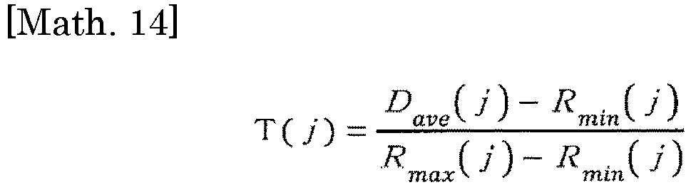
- The wavelength - sensitivity characteristic obtaining process subsequently substitutes this ratio T(j) to the standard spectroscopic image data A and calculates a ratio of absolute value data (the entire column direction).
- More specifically, the wavelength - sensitivity characteristic obtaining process first determines maximum values Pmax(j) and minimum values Pmin(j) with regard to the respective pixel rows (the first row to the m-th row) of the standard spectroscopic image data A. The wavelength - sensitivity characteristic obtaining process subsequently determines the maximum value Pmax(j) at the position of the maximum value Rmax(j) in the column direction and determines the minimum value Pmin(j) at the position of the minimum value Rmin(j) in the column direction. A ratio V(j) of the determined column data is expressed by a relational expression of [Math. 15] given below:

- As a result of the series of processing described above, the wavelength - sensitivity characteristic obtaining process (step S34) obtains the ratio V(j) of the column data and also obtains a number Cy of all luminance value data after exclusion of the invalid data from the standard spectroscopic image data A and a total value Sumy of all the luminance value data after exclusion of the invalid data from the standard spectroscopic image data A, as wavelength - sensitivity characteristics.
- The number Cy of all the luminance value data after exclusion of the invalid data from the standard spectroscopic image data A and the total value Sumy of all the luminance value data after exclusion of the invalid data from the standard spectroscopic image data A are expressed by relational expressions of [Math. 16] given below:
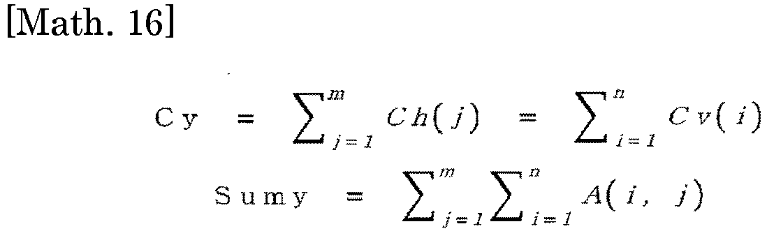
- The
control processing device 54 subsequently performs a correction value calculation process (step S35). This process corresponds to the correction value calculation process according to the embodiment. The processing function of thecontrol processing device 54 that performs this process is configured as the correction value calculation module according to the embodiment. - The correction value calculation process first multiplies the ratio V(i) of the row data obtained at step S33 by the ratio V(j) of the column data obtained at step S34 to implement two-dimensional expansion.
- This obtains, for example, a ratio (distribution) E of all the luminance value data as shown in
Fig. 19 . More specifically, this obtains the "wavelength - sensitivity characteristic by taking into account the width direction - luminance characteristic (luminance unevenness)" at the respective coordinate positions. A ratio E(i,j) with regard to coordinates (i,j) is expressed by a relational expression of [Math. 17] given below:
- The correction value calculation process subsequently calculates an average Eave of the ratio of all the luminance value data. The average Eave is expressed by a relational expression of [Math. 18] given blow:

- The correction value calculation process subsequently determines an average value Fave of all the luminance value data of the standard spectroscopic image data A that are used for calculation of the ratio V(i) of the row data and the ratio V(j) of the column data. The average value Fave is expressed by a relational expression of [Math. 19] given below:

- The correction value calculation process then divides the average value Fave of all the luminance value data by the average Eave of the ratio, so as to determine luminance value data of the standard spectroscopic image data A when the correction value is a Max value of "1". The Max value is expressed by a relational expression of [Math. 20] given below:

- The correction value calculation process subsequently expands this into the ratio E of all the luminance value data shown in
Fig. 19 , so as to obtain virtual corrected image data G as shown inFig. 20 . Corrected luminance value data G(i,j) with regard to each coordinate position (i,j) is expressed by a relational expression of [Math. 21] given below:
- Dividing the corrected luminance value data G(i,j) with regard to each coordinate position (i,j) by the luminance value data of the standard spectroscopic image data A with regard to each coordinate position (i,j) provides a correction value H(i,j) with regard to each coordinate position (i,j) as shown in
Fig. 21 . The correction value H(i,j) with regard to each coordinate position (i,j) is expressed by a relational expression of [Math. 22] given below:
- The correction value setting routine stores the correction value H(i,j) with regard to each coordinate position (i,j) obtained by the correction value calculation process into the set
data storage device 76 serving as the storage unit and is then terminated. - As described above in detail, the configuration of this embodiment has similar functions and advantageous effects to those of the first embodiment described above.
- More specifically, the configuration of this embodiment performs the normalization process to grasp the wavelength sensitivity characteristic of the
imaging element 65 and the luminance characteristic of the imaging area. The configuration of this embodiment thus further enhances the inspection accuracy, compared with the configuration of the first embodiment described above. - Furthermore, the configuration of this embodiment performs the outlier exclusion process and thereby further enhances the inspection accuracy.
- The present disclosure is not limited to the description of the above respective embodiments but may be implemented, for example, by configurations described below. The present disclosure may also be naturally implemented by applications and modifications other than those illustrated below.
- (a) Each of the embodiments described above illustrates the case where the
tablet 5 is the content (inspection object). The type, the shape and the like of the content are, however, not specifically limited. For example, the content may be a capsule, a supplement, or a food item. The tablet includes a solid preparation such as an uncoated tablet and a sugar-coated tablet. - (b) The materials of the
container film 3 and thecover film 4 are not limited to those of the respective embodiments described above, but other materials may be employed. For example, thecontainer film 3 may be formed from a metal material that contains aluminum as a main material, for example, aluminum laminated film. - (c) The arrangement and the number of the
pocket portions 2 in thePTP sheet 1 are not limited at all to those described in the above respective embodiments. A PTP sheet may be configured to have any of various other arrangements of and any number of pocket portions, for example, a total of twelve pocket portions arrayed in three lines. - (d) According to the respective embodiments described above, the
inspection device 22 is configured to perform the different type inclusion inspection in a post process after thetablets 5 are filled in thepocket portions 2 and a previous process before thecover film 4 is mounted to thecontainer film 3.
This configuration is, however, not restrictive. According to a modification, theinspection device 22 may be configured to perform the different type inclusion inspection from the container film 3-side of thePTP film 6, for example, in a post process after thecover film 4 is mounted to thecontainer film 3 and a previous process before thePTP sheets 1 are punched out from thePTP film 6.
According to another modification, theinspection device 22 may be configured to perform the different type inclusion inspection from the container film 3-side of thePTP sheet 1 conveyed by theextraction conveyor 39 in a post process after thePTP sheets 1 are punched out from thePTP film 6.
According to another modification, instead of the (inline) configuration where theinspection device 22 is provided in thePTP packaging machine 10, theinspection device 22 may be provided as a device of performing an offline inspection of thePTP sheet 1, separately from thePTP packaging machine 10. Additionally, theinspection device 22 may be equipped with a conveyance unit to convey thePTP sheet 1.
According to another modification, theinspection device 22 may be configured to perform the different type inclusion inspection in a previous process before thetablets 5 are filled in thepocket portions 2. For example, the inspection may be performed in a stage before thetablets 5 are fed into thetablet filling device 21. In other words, theinspection device 22 may be provided as a device of performing an offline inspection of thetablets 5, separately from thePTP packaging machine 10. - (e) The configurations of the
illumination device 52 and theimaging device 53 are not limited to those described in the above respective embodiments. For example, a reflection type diffraction grating, a prism and the like may be employed as the spectral unit, in place of the two-dimensional spectroscope 62. - (f) According to the respective embodiments described above, the spectral data are analyzed by principal component analysis (PCA). This method is, however, not restrictive. Another known method, such as PLS regression analysis may be employed to analyze the spectral data.
- (g) According to the respective embodiments described above, the correction value setting routine is configured to grasp the wavelength sensitivity characteristic of the
imaging element 65 and the luminance characteristic of the imaging area and to calculate the correction values based on these characteristics. This configuration is, however, not restrictive. A modification may be configured to grasp at least the wavelength sensitivity characteristic of theimaging element 65 and to calculate correction values based on this characteristic. - (h) The details of the wavelength - sensitivity characteristic obtaining process and/or the details of the width direction - luminance characteristic obtaining process are not limited to the configurations described in the above respective embodiments, but other configurations may be employed.
For example, the first embodiment described above is configured to perform the averaging process of averaging the luminance values of pixels belong to a predetermined pixel row or a predetermined pixel column and to specify the calculated average luminance value as the characteristic of the predetermined pixel row or the predetermined pixel column. A modification may be configured, for example, to perform an addition process of summing up the luminance values of pixels belonging to a predetermined pixel row or a predetermined pixel column and to specify the calculated total luminance value as the characteristic of the predetermined pixel row or the predetermined pixel column. - (i) According to the second embodiment described above, the normalization process normalizes, for example, the average to "0" as the first value and the dispersion to "1" as the second value. The first value and/or the second value are, however, not limited to "0" and "1" but may be other values.
- (j) The first embodiment described above may be configured to perform the outlier exclusion process. The second embodiment described above may be configured to omit the outlier exclusion process.
- 1... PTP sheet, 2... pocket portion, 3... container film, 4... cover film, 5... tablet, 10... PTP packaging machine, 22... inspection device, 52... illumination device, 53... imaging device, 54... control processing device, 62... two-dimensional spectroscope, 62a... slit, 63... camera, 64... light-receiving element, 65... imaging element, 74... image data storage device, 76... set data storage device, Ls... optical spectrum
Claims (5)
- An inspection device, comprising:an irradiation unit configured to irradiate an object with near-infrared light;a spectral unit configured to disperse reflected light that is reflected from the object irradiated with the near-infrared light; andan imaging unit provided with an imaging element that includes a plurality of light-receiving elements arranged in a matrix arrangement and configured to take an image of an optical spectrum of the reflected light dispersed by the spectral unit,the inspection device being configured to perform a predetermined inspection by taking advantage of spectral analysis, based on spectroscopic image data obtained by the imaging unit,the inspection device further comprising:a wavelength sensitivity characteristic grasping module configured to perform a predetermined arithmetic operation, with regard to each pixel row that is perpendicular to a wavelength dispersion direction of the optical spectrum and/or each pixel column that is parallel to the wavelength dispersion direction in standard spectroscopic image data obtained by taking an image of an optical spectrum of a predetermined standard object by the imaging unit, by using luminance values of pixels belonging to the pixel row or belonging to the pixel column, so as to determine a characteristic of each pixel row and thereby grasp a wavelength sensitivity characteristic of the imaging element under the near-infrared light emitted from the irradiation unit;a correction value calculation module configured to calculate a correction value with regard to each coordinate position corresponding to each pixel of the standard spectroscopic image data, based on a luminance value of each pixel of the standard spectroscopic image data and the characteristic with regard to a pixel row which the pixel belongs to;an image correction module configured to correct a luminance value of each pixel of inspection spectroscopic image data obtained by taking an image of a predetermined inspection object by the imaging unit, based on the correction value with regard to the coordinate position corresponding to the pixel;a spectral data obtaining module configured to obtain spectral data, based on corrected spectroscopic image data obtained by correcting the inspection spectroscopic image data; andan analysis module configured to perform a predetermined analysis process with regard to the inspection object, based on the spectral data.
- An inspection device, comprising:an irradiation unit configured to irradiate an object with near-infrared light;a spectral unit configured to disperse reflected light that is reflected from the object irradiated with the near-infrared light; andan imaging unit provided with an imaging element that includes a plurality of light-receiving elements arranged in a matrix arrangement and configured to take an image of an optical spectrum of the reflected light dispersed by the spectral unit,the inspection device being configured to perform a predetermined inspection by taking advantage of spectral analysis, based on spectroscopic image data obtained by the imaging unit,the inspection device further comprising:a wavelength sensitivity characteristic grasping module configured to perform a predetermined arithmetic operation, with regard to each pixel row that is perpendicular to a wavelength dispersion direction of the optical spectrum and/or each pixel column that is parallel to the wavelength dispersion direction in standard spectroscopic image data obtained by taking an image of an optical spectrum of a predetermined standard object by the imaging unit, by using luminance values of pixels belonging to the pixel row or belonging to the pixel column, so as to determine a characteristic of each pixel row and thereby grasp a wavelength sensitivity characteristic of the imaging element under the near-infrared light emitted from the irradiation unit;an imaging area luminance characteristic grasping module configured to perform a predetermined arithmetic operation, with regard to each pixel column that is parallel to the wavelength dispersion direction and/or each pixel row that is perpendicular to the wavelength dispersion direction in the standard spectroscopic image data, by using luminance values of pixels belonging to the pixel column or belonging to the pixel row, so as to determine a characteristic of each pixel column and thereby grasp a luminance characteristic in an imaging area under the near-infrared light emitted from the irradiation unit;a correction value calculation module configured to calculate a correction value with regard to each coordinate position corresponding to each pixel of the standard spectroscopic image data, based on a luminance value of each pixel of the standard spectroscopic image data, the characteristic with regard to a pixel row which the pixel belongs to, and the characteristic with regard to a pixel column which the pixel belongs to;an image correction module configured to correct a luminance value of each pixel of inspection spectroscopic image data obtained by taking an image of a predetermined inspection object by the imaging unit, based on the correction value with regard to the coordinate position corresponding to the pixel;a spectral data obtaining module configured to obtain spectral data, based on corrected spectroscopic image data obtained by correcting the inspection spectroscopic image data; andan analysis module configured to perform a predetermined analysis process with regard to the inspection object, based on the spectral data.
- A PTP packaging machine configured to manufacture a PTP sheet such that a predetermined content is contained in a pocket portion formed in a container film and that a cover film is mounted to the container film, so as to close the pocket portion,
the PTP packaging machine comprising:a pocket portion forming unit configured to form the pocket portion in the container film that is conveyed in a belt-like manner;a filling unit configured to fill the content into the pocket portion;a mounting unit configured to mount the cover film in a belt-like shape to the container film with the pocket portion filled with the content, so as to close the pocket portions;a separation unit configured to separate the PTP sheet from a belt-like body obtained by mounting the cover film to the container film; andthe inspection device according to either claim 1 or claim 2 configured to perform an inspection with specifying the content as the inspection object. - A calibration method of an inspection device,
wherein the inspection device comprises an irradiation unit configured to irradiate an object with near-infrared light; a spectral unit configured to disperse reflected light that is reflected from the object irradiated with the near-infrared light; and an imaging unit provided with an imaging element that includes a plurality of light-receiving elements arranged in a matrix arrangement and configured to take an image of an optical spectrum of the reflected light dispersed by the spectral unit, and
wherein the inspection device is configured to perform a predetermined inspection by taking advantage of spectral analysis, based on spectroscopic image data obtained by the imaging unit,
the calibration method comprising:a wavelength sensitivity characteristic grasping process of performing a predetermined arithmetic operation, with regard to each pixel row that is perpendicular to a wavelength dispersion direction of the optical spectrum and/or each pixel column that is parallel to the wavelength dispersion direction in standard spectroscopic image data obtained by taking an image of an optical spectrum of a predetermined standard object by the imaging unit, by using luminance values of pixels belonging to the pixel row or belonging to the pixel column, so as to determine a characteristic of each pixel row and thereby grasp a wavelength sensitivity characteristic of the imaging element under the near-infrared light emitted from the irradiation unit;a correction value calculation process of calculating a correction value with regard to each coordinate position corresponding to each pixel of the standard spectroscopic image data, based on a luminance value of each pixel of the standard spectroscopic image data and the characteristic with regard to a pixel row which the pixel belongs to; andan image correction process of correcting a luminance value of each pixel of inspection spectroscopic image data obtained by taking an image of a predetermined inspection object by the imaging unit, based on the correction value with regard to the coordinate position corresponding to the pixel. - A calibration method of an inspection device,
wherein the inspection device comprises an irradiation unit configured to irradiate an object with near-infrared light; a spectral unit configured to disperse reflected light that is reflected from the object irradiated with the near-infrared light; and an imaging unit provided with an imaging element that includes a plurality of light-receiving elements arranged in a matrix arrangement and configured to take an image of an optical spectrum of the reflected light dispersed by the spectral unit, and
wherein the inspection device is configured to perform a predetermined inspection by taking advantage of spectral analysis, based on spectroscopic image data obtained by the imaging unit,
the calibration method comprising:a wavelength sensitivity characteristic grasping process of performing a predetermined arithmetic operation, with regard to each pixel row that is perpendicular to a wavelength dispersion direction of the optical spectrum and/or each pixel column that is parallel to the wavelength dispersion direction in standard spectroscopic image data obtained by taking an image of an optical spectrum of a predetermined standard object by the imaging unit, by using luminance values of pixels belonging to the pixel row or belonging to the pixel column, so as to determine a characteristic of each pixel row and thereby grasp a wavelength sensitivity characteristic of the imaging element under the near-infrared light emitted from the irradiation unit;an imaging area luminance characteristic grasping process of performing a predetermined arithmetic operation, with regard to each pixel column that is parallel to the wavelength dispersion direction and/or each pixel row that is perpendicular to the wavelength dispersion direction in the standard spectroscopic image data, by using luminance values of pixels belonging to the pixel column or belonging to the pixel row, so as to determine a characteristic of each pixel column and thereby grasp a luminance characteristic in an imaging area under the near-infrared light emitted from the irradiation unit;a correction value calculation process of calculating a correction value with regard to each coordinate position corresponding to each pixel of the standard spectroscopic image data, based on a luminance value of each pixel of the standard spectroscopic image data, the characteristic with regard to a pixel row which the pixel belongs to, and the characteristic with regard to a pixel column which the pixel belongs to; andan image correction process of correcting a luminance value of each pixel of inspection spectroscopic image data obtained by taking an image of a predetermined inspection object by the imaging unit, based on the correction value with regard to the coordinate position corresponding to the pixel.
Applications Claiming Priority (2)
| Application Number | Priority Date | Filing Date | Title |
|---|---|---|---|
| JP2018009794A JP6568245B2 (en) | 2018-01-24 | 2018-01-24 | Inspection device, PTP packaging machine, and calibration method for inspection device |
| PCT/JP2018/033210 WO2019146152A1 (en) | 2018-01-24 | 2018-09-07 | Inspection device, ptp packaging machine, and calibration method of inspection device |
Publications (3)
| Publication Number | Publication Date |
|---|---|
| EP3745113A1 true EP3745113A1 (en) | 2020-12-02 |
| EP3745113A4 EP3745113A4 (en) | 2021-10-20 |
| EP3745113B1 EP3745113B1 (en) | 2026-02-18 |
Family
ID=67395929
Family Applications (1)
| Application Number | Title | Priority Date | Filing Date |
|---|---|---|---|
| EP18902271.8A Active EP3745113B1 (en) | 2018-01-24 | 2018-09-07 | Inspection device, ptp packaging machine, and calibration method of inspection device |
Country Status (5)
| Country | Link |
|---|---|
| US (1) | US12007331B2 (en) |
| EP (1) | EP3745113B1 (en) |
| JP (1) | JP6568245B2 (en) |
| CN (1) | CN111630369B (en) |
| WO (1) | WO2019146152A1 (en) |
Cited By (1)
| Publication number | Priority date | Publication date | Assignee | Title |
|---|---|---|---|---|
| EP4647238A1 (en) | 2024-05-06 | 2025-11-12 | WM Thermoforming Machines SA | Thermoforming machine |
Families Citing this family (5)
| Publication number | Priority date | Publication date | Assignee | Title |
|---|---|---|---|---|
| JP6763059B1 (en) * | 2019-05-16 | 2020-09-30 | Ckd株式会社 | Inspection equipment, packaging machine and packaging inspection method |
| NL2027213B1 (en) * | 2020-12-03 | 2022-07-06 | Ziuz Holding B V | Inspecting medicine objects based on hyperspectral imaging |
| JP7768990B2 (en) * | 2020-12-03 | 2025-11-12 | パラタ システムズ,エルエルシー | Inspection of pharmaceutical objects based on hyperspectral imaging |
| KR102531177B1 (en) * | 2021-03-29 | 2023-05-10 | (주)크레템 | Cover attaching unit for blister pack and apparatus for automatically blister-packing medicines |
| JP7429205B2 (en) * | 2021-05-13 | 2024-02-07 | アンリツ株式会社 | Article inspection equipment |
Family Cites Families (30)
| Publication number | Priority date | Publication date | Assignee | Title |
|---|---|---|---|---|
| JPS58103604A (en) * | 1981-12-16 | 1983-06-20 | Teijin Ltd | Method and device for measuring thickness of film |
| US5131755A (en) * | 1988-02-19 | 1992-07-21 | Chadwick Curt H | Automatic high speed optical inspection system |
| JP2558864B2 (en) * | 1989-02-27 | 1996-11-27 | 浜松ホトニクス株式会社 | Spectroscopic analyzer |
| JPH0432729A (en) | 1990-05-30 | 1992-02-04 | Denki Kagaku Keiki Kk | Fourier transformation type spectral analyzing device |
| SE512098C2 (en) * | 1998-05-19 | 2000-01-24 | Agrovision Ab | Concentration determination of one component in a mixture of at least two components |
| JP2003107008A (en) * | 2001-09-28 | 2003-04-09 | Web Tec Kk | Method for detecting density and surface state of printing sheet |
| US7459696B2 (en) * | 2003-04-18 | 2008-12-02 | Schomacker Kevin T | Methods and apparatus for calibrating spectral data |
| JP5103736B2 (en) * | 2003-10-17 | 2012-12-19 | アステラス製薬株式会社 | Heterogeneous product detection device using a planar spectrometer |
| JP3931875B2 (en) * | 2003-10-29 | 2007-06-20 | 財団法人雑賀技術研究所 | Spectrophotometer |
| JP2006170669A (en) * | 2004-12-13 | 2006-06-29 | Mitsui Mining & Smelting Co Ltd | Fruit and vegetable quality inspection equipment |
| JP2006262274A (en) * | 2005-03-18 | 2006-09-28 | Seiko Epson Corp | Imaging data correction method, imaging data correction apparatus, imaging object inspection method, imaging object inspection apparatus, imaging data correction program, recording medium |
| US8144320B2 (en) * | 2006-11-22 | 2012-03-27 | Optopo, Inc. | Method and apparatus for reconstructing optical spectra in a static multimode multiplex spectrometer |
| JP2009224971A (en) * | 2008-03-14 | 2009-10-01 | Omron Corp | Image processing device |
| JP5206335B2 (en) * | 2008-11-07 | 2013-06-12 | アステラス製薬株式会社 | Principal component analysis method, principal component analysis apparatus, heterogeneous product detection apparatus, principal component analysis program, and recording medium on which principal component analysis program is recorded |
| JP5826452B2 (en) * | 2009-02-02 | 2015-12-02 | 株式会社ミューチュアル | Inspection device |
| EP2498073A1 (en) * | 2009-11-04 | 2012-09-12 | Nireco Corporation | Spectral information read device |
| JP2012088199A (en) * | 2010-10-20 | 2012-05-10 | Yamaha Motor Co Ltd | Method and apparatus for inspecting foreign matter |
| CA2840564A1 (en) * | 2011-06-28 | 2013-01-03 | Otsuka Pharmaceutical Co., Ltd. | Drug inspection device and drug inspection method |
| JP5526183B2 (en) * | 2012-04-25 | 2014-06-18 | Ckd株式会社 | Inspection device and PTP packaging machine |
| JP5697168B2 (en) * | 2012-08-07 | 2015-04-08 | Ckd株式会社 | Inspection device and PTP packaging machine |
| US9546904B2 (en) * | 2013-03-15 | 2017-01-17 | P & P Optica Inc. | Apparatus and method for optimizing data capture and data correction for spectroscopic analysis |
| JP2014215177A (en) * | 2013-04-25 | 2014-11-17 | 住友電気工業株式会社 | Inspection device and inspection method |
| JP6068375B2 (en) * | 2014-03-03 | 2017-01-25 | エバ・ジャパン 株式会社 | Spectral radiance meter |
| JP5917711B2 (en) * | 2014-03-11 | 2016-05-18 | 株式会社東芝 | Tablet inspection device, tablet inspection method, tablet inspection program |
| JP6295798B2 (en) * | 2014-04-11 | 2018-03-20 | 住友電気工業株式会社 | Inspection method |
| JP6254055B2 (en) * | 2014-08-25 | 2017-12-27 | Ckd株式会社 | PTP packaging machine |
| JP6225144B2 (en) * | 2015-02-26 | 2017-11-01 | Ckd株式会社 | PTP sheet manufacturing apparatus and PTP sheet manufacturing method |
| US10281408B2 (en) * | 2016-04-12 | 2019-05-07 | Nippon Steel & Sumitomo Metal Corporation | Inspection object imaging apparatus, inspection object imaging method, surface inspection apparatus, and surface inspection method |
| JP6235684B1 (en) * | 2016-11-29 | 2017-11-22 | Ckd株式会社 | Inspection device and PTP packaging machine |
| JP6706301B2 (en) * | 2018-09-28 | 2020-06-03 | Ckd株式会社 | Inspection device, PTP packaging machine, and PTP sheet manufacturing method |
-
2018
- 2018-01-24 JP JP2018009794A patent/JP6568245B2/en active Active
- 2018-09-07 CN CN201880087558.4A patent/CN111630369B/en active Active
- 2018-09-07 EP EP18902271.8A patent/EP3745113B1/en active Active
- 2018-09-07 WO PCT/JP2018/033210 patent/WO2019146152A1/en not_active Ceased
-
2020
- 2020-07-02 US US16/919,490 patent/US12007331B2/en active Active
Cited By (1)
| Publication number | Priority date | Publication date | Assignee | Title |
|---|---|---|---|---|
| EP4647238A1 (en) | 2024-05-06 | 2025-11-12 | WM Thermoforming Machines SA | Thermoforming machine |
Also Published As
| Publication number | Publication date |
|---|---|
| JP6568245B2 (en) | 2019-08-28 |
| EP3745113B1 (en) | 2026-02-18 |
| CN111630369B (en) | 2023-05-30 |
| US20200333256A1 (en) | 2020-10-22 |
| JP2019128250A (en) | 2019-08-01 |
| EP3745113A4 (en) | 2021-10-20 |
| CN111630369A (en) | 2020-09-04 |
| US12007331B2 (en) | 2024-06-11 |
| WO2019146152A1 (en) | 2019-08-01 |
Similar Documents
| Publication | Publication Date | Title |
|---|---|---|
| US12007331B2 (en) | Inspection device, PTP packaging machine and calibration method of inspection device | |
| US11214396B2 (en) | Inspection device, PTP packaging machine and PTP sheet manufacturing method | |
| US11808714B2 (en) | Inspection device, blister packaging machine, and blister sheet manufacturing method | |
| US11360033B2 (en) | Inspection apparatus, PTP packaging machine, and method for manufacturing PTP sheet | |
| US20190279350A1 (en) | Inspection device and ptp packaging machine | |
| US11338950B2 (en) | Inspection device, PTP packaging machine and PTP sheet manufacturing method | |
| US11981469B2 (en) | Inspection device, PTP packaging machine and inspection method | |
| KR102362846B1 (en) | Inspection device, PTP packaging machine, and method of manufacturing PTP sheet | |
| US11414231B2 (en) | Inspection device and PTP packaging machine | |
| US11448591B2 (en) | Inspection device, PTP packaging machine and inspection method | |
| JP2018159662A (en) | Inspection apparatus, PTP packaging machine, and PTP sheet manufacturing method |
Legal Events
| Date | Code | Title | Description |
|---|---|---|---|
| STAA | Information on the status of an ep patent application or granted ep patent |
Free format text: STATUS: THE INTERNATIONAL PUBLICATION HAS BEEN MADE |
|
| PUAI | Public reference made under article 153(3) epc to a published international application that has entered the european phase |
Free format text: ORIGINAL CODE: 0009012 |
|
| STAA | Information on the status of an ep patent application or granted ep patent |
Free format text: STATUS: REQUEST FOR EXAMINATION WAS MADE |
|
| 17P | Request for examination filed |
Effective date: 20200528 |
|
| AK | Designated contracting states |
Kind code of ref document: A1 Designated state(s): AL AT BE BG CH CY CZ DE DK EE ES FI FR GB GR HR HU IE IS IT LI LT LU LV MC MK MT NL NO PL PT RO RS SE SI SK SM TR |
|
| AX | Request for extension of the european patent |
Extension state: BA ME |
|
| DAV | Request for validation of the european patent (deleted) | ||
| DAX | Request for extension of the european patent (deleted) | ||
| A4 | Supplementary search report drawn up and despatched |
Effective date: 20210922 |
|
| RIC1 | Information provided on ipc code assigned before grant |
Ipc: G06T 7/00 20170101ALI20210916BHEP Ipc: B65B 9/04 20060101ALI20210916BHEP Ipc: G01N 21/3563 20140101ALI20210916BHEP Ipc: B29L 31/00 20060101ALI20210916BHEP Ipc: B29C 51/46 20060101ALI20210916BHEP Ipc: B29C 51/18 20060101ALI20210916BHEP Ipc: B29C 51/26 20060101ALI20210916BHEP Ipc: G01N 21/95 20060101ALI20210916BHEP Ipc: G01N 21/93 20060101ALI20210916BHEP Ipc: G06T 7/80 20170101ALI20210916BHEP Ipc: G01N 21/85 20060101ALI20210916BHEP Ipc: G01N 21/359 20140101ALI20210916BHEP Ipc: B65B 57/10 20060101ALI20210916BHEP Ipc: G01N 21/27 20060101AFI20210916BHEP |
|
| STAA | Information on the status of an ep patent application or granted ep patent |
Free format text: STATUS: EXAMINATION IS IN PROGRESS |
|
| 17Q | First examination report despatched |
Effective date: 20230929 |
|
| GRAP | Despatch of communication of intention to grant a patent |
Free format text: ORIGINAL CODE: EPIDOSNIGR1 |
|
| STAA | Information on the status of an ep patent application or granted ep patent |
Free format text: STATUS: GRANT OF PATENT IS INTENDED |
|
| INTG | Intention to grant announced |
Effective date: 20250919 |
|
| GRAS | Grant fee paid |
Free format text: ORIGINAL CODE: EPIDOSNIGR3 |
|
| GRAA | (expected) grant |
Free format text: ORIGINAL CODE: 0009210 |
|
| STAA | Information on the status of an ep patent application or granted ep patent |
Free format text: STATUS: THE PATENT HAS BEEN GRANTED |
|
| AK | Designated contracting states |
Kind code of ref document: B1 Designated state(s): AL AT BE BG CH CY CZ DE DK EE ES FI FR GB GR HR HU IE IS IT LI LT LU LV MC MK MT NL NO PL PT RO RS SE SI SK SM TR |
|
| REG | Reference to a national code |
Ref country code: CH Ref legal event code: F10 Free format text: ST27 STATUS EVENT CODE: U-0-0-F10-F00 (AS PROVIDED BY THE NATIONAL OFFICE) Effective date: 20260218 Ref country code: GB Ref legal event code: FG4D |
|
| REG | Reference to a national code |
Ref country code: IE Ref legal event code: FG4D |
|
| REG | Reference to a national code |
Ref country code: DE Ref legal event code: R096 Ref document number: 602018089299 Country of ref document: DE |