EP3742557A1 - Smd-fähige tht-aufnahme - Google Patents
Smd-fähige tht-aufnahme Download PDFInfo
- Publication number
- EP3742557A1 EP3742557A1 EP20173793.9A EP20173793A EP3742557A1 EP 3742557 A1 EP3742557 A1 EP 3742557A1 EP 20173793 A EP20173793 A EP 20173793A EP 3742557 A1 EP3742557 A1 EP 3742557A1
- Authority
- EP
- European Patent Office
- Prior art keywords
- circuit board
- contact part
- opening
- bfe1
- connection
- Prior art date
- Legal status (The legal status is an assumption and is not a legal conclusion. Google has not performed a legal analysis and makes no representation as to the accuracy of the status listed.)
- Pending
Links
- 239000000463 material Substances 0.000 claims abstract description 24
- 239000002184 metal Substances 0.000 claims description 14
- 229910052751 metal Inorganic materials 0.000 claims description 14
- 229910000881 Cu alloy Inorganic materials 0.000 claims description 4
- 238000005476 soldering Methods 0.000 description 21
- 238000000034 method Methods 0.000 description 17
- 238000005516 engineering process Methods 0.000 description 7
- 238000004519 manufacturing process Methods 0.000 description 7
- 239000003990 capacitor Substances 0.000 description 6
- RYGMFSIKBFXOCR-UHFFFAOYSA-N Copper Chemical compound [Cu] RYGMFSIKBFXOCR-UHFFFAOYSA-N 0.000 description 4
- 239000002131 composite material Substances 0.000 description 4
- 229910052802 copper Inorganic materials 0.000 description 4
- 239000010949 copper Substances 0.000 description 4
- 239000000853 adhesive Substances 0.000 description 2
- 230000001070 adhesive effect Effects 0.000 description 2
- 238000003780 insertion Methods 0.000 description 2
- 230000037431 insertion Effects 0.000 description 2
- 230000000873 masking effect Effects 0.000 description 2
- 229910000679 solder Inorganic materials 0.000 description 2
- 229920002430 Fibre-reinforced plastic Polymers 0.000 description 1
- 239000004020 conductor Substances 0.000 description 1
- 238000005260 corrosion Methods 0.000 description 1
- 230000007797 corrosion Effects 0.000 description 1
- 238000005520 cutting process Methods 0.000 description 1
- 238000005553 drilling Methods 0.000 description 1
- 239000003822 epoxy resin Substances 0.000 description 1
- 238000005530 etching Methods 0.000 description 1
- 239000011151 fibre-reinforced plastic Substances 0.000 description 1
- 239000011521 glass Substances 0.000 description 1
- 239000004033 plastic Substances 0.000 description 1
- 229920003023 plastic Polymers 0.000 description 1
- 229920000647 polyepoxide Polymers 0.000 description 1
- 238000000742 single-metal deposition Methods 0.000 description 1
- 238000005482 strain hardening Methods 0.000 description 1
- 239000000758 substrate Substances 0.000 description 1
Images


Classifications
-
- H—ELECTRICITY
- H01—ELECTRIC ELEMENTS
- H01R—ELECTRICALLY-CONDUCTIVE CONNECTIONS; STRUCTURAL ASSOCIATIONS OF A PLURALITY OF MUTUALLY-INSULATED ELECTRICAL CONNECTING ELEMENTS; COUPLING DEVICES; CURRENT COLLECTORS
- H01R12/00—Structural associations of a plurality of mutually-insulated electrical connecting elements, specially adapted for printed circuits, e.g. printed circuit boards [PCB], flat or ribbon cables, or like generally planar structures, e.g. terminal strips, terminal blocks; Coupling devices specially adapted for printed circuits, flat or ribbon cables, or like generally planar structures; Terminals specially adapted for contact with, or insertion into, printed circuits, flat or ribbon cables, or like generally planar structures
- H01R12/50—Fixed connections
- H01R12/51—Fixed connections for rigid printed circuits or like structures
- H01R12/55—Fixed connections for rigid printed circuits or like structures characterised by the terminals
- H01R12/58—Fixed connections for rigid printed circuits or like structures characterised by the terminals terminals for insertion into holes
-
- H—ELECTRICITY
- H01—ELECTRIC ELEMENTS
- H01R—ELECTRICALLY-CONDUCTIVE CONNECTIONS; STRUCTURAL ASSOCIATIONS OF A PLURALITY OF MUTUALLY-INSULATED ELECTRICAL CONNECTING ELEMENTS; COUPLING DEVICES; CURRENT COLLECTORS
- H01R4/00—Electrically-conductive connections between two or more conductive members in direct contact, i.e. touching one another; Means for effecting or maintaining such contact; Electrically-conductive connections having two or more spaced connecting locations for conductors and using contact members penetrating insulation
- H01R4/28—Clamped connections, spring connections
- H01R4/48—Clamped connections, spring connections utilising a spring, clip, or other resilient member
-
- H—ELECTRICITY
- H01—ELECTRIC ELEMENTS
- H01R—ELECTRICALLY-CONDUCTIVE CONNECTIONS; STRUCTURAL ASSOCIATIONS OF A PLURALITY OF MUTUALLY-INSULATED ELECTRICAL CONNECTING ELEMENTS; COUPLING DEVICES; CURRENT COLLECTORS
- H01R12/00—Structural associations of a plurality of mutually-insulated electrical connecting elements, specially adapted for printed circuits, e.g. printed circuit boards [PCB], flat or ribbon cables, or like generally planar structures, e.g. terminal strips, terminal blocks; Coupling devices specially adapted for printed circuits, flat or ribbon cables, or like generally planar structures; Terminals specially adapted for contact with, or insertion into, printed circuits, flat or ribbon cables, or like generally planar structures
- H01R12/50—Fixed connections
- H01R12/51—Fixed connections for rigid printed circuits or like structures
- H01R12/53—Fixed connections for rigid printed circuits or like structures connecting to cables except for flat or ribbon cables
-
- Y—GENERAL TAGGING OF NEW TECHNOLOGICAL DEVELOPMENTS; GENERAL TAGGING OF CROSS-SECTIONAL TECHNOLOGIES SPANNING OVER SEVERAL SECTIONS OF THE IPC; TECHNICAL SUBJECTS COVERED BY FORMER USPC CROSS-REFERENCE ART COLLECTIONS [XRACs] AND DIGESTS
- Y02—TECHNOLOGIES OR APPLICATIONS FOR MITIGATION OR ADAPTATION AGAINST CLIMATE CHANGE
- Y02P—CLIMATE CHANGE MITIGATION TECHNOLOGIES IN THE PRODUCTION OR PROCESSING OF GOODS
- Y02P70/00—Climate change mitigation technologies in the production process for final industrial or consumer products
- Y02P70/50—Manufacturing or production processes characterised by the final manufactured product
Definitions
- the invention relates to a device suitable for a material connection with a printed circuit board.
- the object is achieved by a device suitable for a material connection with a printed circuit board, the device having an opening for receiving a contact part (pin), the opening being delimited by leaf spring elements, with a through the opening when the contact part is received frictional connection of the contact part with the leaf spring elements and electrical contacting of the contact part with the device can be or is made.
- the device enables wired components such as resistors, electrolytic capacitors, to be placed on a circuit board without having to use a new soldering process (e.g. wave soldering).
- the device fixes the component mechanically, but advantageously also establishes the electrical contact. A soldering process can thus be saved.
- the device itself is advantageously applied to the circuit carrier, the PCB (printed circuit board; printed circuit board, printed circuit board, circuit board or printed circuit) using an SMD soldering process.
- a first advantageous embodiment of the invention is that the device has the opening for receiving the contact part (pin) essentially in the middle. As a result, the device has high stability despite the opening.
- Another advantageous embodiment of the invention is that the opening is delimited by two mutually opposite leaf spring elements.
- the spring action of the leaf spring elements makes it easy to establish a non-positive connection and contact.
- the device is a correspondingly designed metal plate.
- a metal plate can be firmly connected to the circuit board.
- the metal plate is a correspondingly stamped or shaped metal plate.
- the device itself can thus be manufactured inexpensively, for example as a stamped, advantageously tinned copper sheet.
- the metal plate has a copper alloy.
- the copper alloy ensures high strength, deformability, strain hardening, corrosion resistance and good sliding properties for the device.
- contact part is fixed on the circuit board by the force-fit connection.
- the non-positive connection thus simultaneously ensures the mechanical fixing and the electrical contacting of the component to be assembled on the circuit board.
- a separate contact e.g. by wiring is not necessary.
- the material connection between the device and the circuit board is made by a soldered connection.
- suitable SMD soldering processes e.g. Reflow soldering, reflow soldering or corresponding soft soldering processes.
- a further advantageous embodiment of the invention is that the device is applied to the rear side of the circuit board by the material connection on the circuit board. As a result, the device does not interfere with the architecture or the topology of the circuit board.
- Another advantageous embodiment of the invention is a printed circuit board, suitable for a material connection with at least one device according to the invention.
- the device can be used for any printed circuit boards.
- the circuit board can for example consist of fiber-reinforced plastic (eg fiber-plastic composite (FRP)) or a glass fiber-epoxy resin composite, eg FR4.
- FRP fiber-plastic composite
- FR4 glass fiber-epoxy resin composite
- a further advantageous embodiment of the invention is that the circuit board has two footprint pads arranged adjacent to one another for the material connection with the device.
- the footprint pads arranged adjacent to one another are advantageously spaced apart such that a corresponding hole or via can be made between the footprint pads.
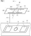
- Figure 1 shows a first exemplary device VO1, suitable for a material connection with a circuit board LP1.
- the device VO1 is suitable for a material connection with a printed circuit board LP1, the device VO1 having an opening OE1 for receiving a contact part (pin), the opening OE1 being delimited by leaf spring elements BFE1, BFE1 ', whereby when the contact part is received by through the opening OE1 a non-positive connection of the contact part with the leaf spring elements BFE1, BFE1 'and, at the same time, an electrical contact between the contact part and the device VO1 can be or is made.
- the representation according to Figure 1 shows the rear of a printed circuit board.
- the material of the device VO1 can be, for example, a stamped (advantageously tinned) copper plate as a metal plate.
- the arrow PF1 indicates that the device VO1 is being applied to the circuit board LP1.
- the device VO1 can be applied to footprint pads FP1, FP2, for example by means of a suitable adhesive or soldered connection, and fastened to the circuit board LP1. Standard footprints, eg 1210 with solder paste or wetted solder pads, can be used for this.
- the circuit board LP1 can for example consist of the composite material of class FR4.
- the footprint pads FP1, FP2 are also referred to as landing pads and represent SMD contact surfaces for the device VO1 on the circuit board LP1.
- the footprint pads FP1, FP2 are advantageously arranged on the circuit board LP1 in such a way that the end regions EB1 , EB2 of the device VO1 are positioned on the footprint pads FP1, FP2 after the device VO1 has been attached or applied to the circuit board LP1.
- the footprint pads FP1, FP2 are advantageously electrically contacted with the components or components on the circuit board LP1.
- the footprint pads FP1, FP2 each of a device VO1 advantageously have the same electrical potential.
- Footprint pads FP1, FP2 are advantageous Footprint pads FP1, FP2 as well as the intermediate bore B1 (or via) attached or positioned in alignment with one another on the circuit board LP1.
- the footprint pads FP1, FP2 and the hole B1 in between are advantageously spaced apart on one axis.
- the respective footprint pads FP1, FP2 are advantageously created on the circuit board LP1 by appropriate masking or masking steps (for example, according to a corresponding copper etching process).
- the respective end regions EB1, EB2 of the device VO1 are attached to the respective footprint pads FP1, FP2 by suitable connecting means (for example, by a suitable soldered or adhesive connection).
- the device VO1 is advantageously attached to the rear of the printed circuit board LP1, which is opposite the component side.
- the device VO1 can also be arranged on the component side of the printed circuit board LP1. In this case, after the pin has been moved, the leaf spring elements of the device VO1 protrude into a corresponding recess (e.g. blind hole) in the circuit board LP1.
- a corresponding recess e.g. blind hole
- the opening OE1 of the device VO1 is advantageously made essentially centrally over the bore B1.
- the opening OE1 does not necessarily have to be located in the center of the device VO1.
- the hole B1 is located on the circuit board LP1 and is used to accommodate the contact part (eg pin) of a component, eg in THT technology (through-hole technology).
- the opening B1 can be a bore or a via.
- a via or a via or a via is a vertical electrical connection between the conductor track levels of a circuit board. The connection is realized, for example, through an internally metallized hole in the substrate of the printed circuit board.
- the bore or via B1 advantageously has only a small residual ring with regard to the diameter of the contact part to be inserted (e.g. pin).
- the dashed line represents an axis AC perpendicular or essentially perpendicular to the device VO1, for example an insertion or lead-through axis for the contact parts (pins) or vias to be introduced or passed through.
- the device VO1 enables a contact part (pin) or a via to be fastened or connectable on a printed circuit board LP1 using clamping technology or using clamping cutting technology.
- the device VO1 has the opening OE1 for receiving the contact part (pin) essentially in the center.
- An advantageous embodiment of the invention is that the opening OE1 is delimited by two mutually opposite leaf spring elements BFE1, BFE1 '.
- the device VO1 is a correspondingly configured metal plate.
- metal plate is a correspondingly stamped or shaped metal plate.
- An advantageous embodiment of the invention is that the metal plate has a copper alloy.
- An advantageous embodiment of the invention is that the contact part is fixed or is fixed on the circuit board LP1 by the force-fit connection.
- An advantageous embodiment of the invention is that the material connection between the device VO1 and the circuit board LP1 is made by a soldered connection.
- An advantageous embodiment of the invention is that the device VO1 is applied to the back of the circuit board LP1 through the material connection on the circuit board LP1.
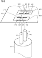
- Figure 2 shows second exemplary devices VO2, VO2 ', suitable for a material connection to a printed circuit board LP2.
- the devices VO2, VO2 ' are each suitable for a respective material connection with a printed circuit board LP2, the devices VO2, VO2' each having an opening OE2, OE2 'for receiving a contact part (pin) P1, P2 of a component BT1 (e.g.
- OE2 Electrolytic capacitor body
- the arrows PF2-PF4 represent the insertion direction or the push-through direction of the contact parts P1, P1 'of the component or of the component BT1.
- the openings OE2, OE2 ' are advantageously each arranged essentially centrally above the respective bores B2, B2' or via.
- the openings OE2, OE2 ' are advantageously each delimited by two mutually opposite leaf spring elements BFE2, BFE2' or BFE3, BFE3 '.
- the representation according to Figure 2 shows the rear of a printed circuit board.
- Figure 3 shows third exemplary devices VO3, VO3 ', suitable for a respective material connection to a printed circuit board LP3.
- the devices VO3, VO3 ' are each suitable for a respective material connection with a printed circuit board LP3, the devices VO3, VO3' each having an opening OE3, OE3 'for receiving a contact part (pin) P2, P2' of a component BT2 (e.g.
- the respective openings OE3, OE3 ' are each delimited by leaf spring elements BFE4, BFE4' or BFE5, BFE5 ', wherein when a contact part P2, P2' is received in the respective opening OE3, OE3 'a non-positive connection of the respective contact part P2, P2 'with the respective leaf spring elements BFE4, BFE4' or BFE5, BFE5 'and electrical contacting of the contact part P2, P2' with the device VO3 or VO3 'can be produced.
- the openings OE3, OE3 ' are advantageously each arranged essentially centrally above the respective bores B3, B3' or via.
- the openings OE3, OE3 ' are advantageously each delimited by two mutually opposite leaf spring elements BFE4, BFE4' or BFE5, BFE5 '.
- FIG. 3 shows the rear side of a flat module, the contact parts P2, P2 'of the component BT2 making contact with the circuit board LP3 through the leaf spring elements BFE4, BFE4' or BFE5, BFE5 '.
- Figure 4 shows a fourth exemplary device VO4 with exemplary dimensions (dimensions) in mm.
- the fourth exemplary device VO4 has leaf spring elements BFE6, BFE6 'and an opening OE4.
- Figure 5 shows in the left part of the figure a table T with exemplary specifications for dimensions A, B, C, D for the layout of footprint pads FP3, FP4 as a function of a standardized exemplary SMD component BT3.
- the dimension A represents the respective distance between the footprint pads FP3 and FP4 on the circuit board.
- the left column in the table T lists the corresponding exemplary standardized components BT3.
- the columns A, B, C, D show the recommended exemplary dimensions for the respective component BT3.
- Table T shows recommended exemplary footprint layout dimensions for respective components BT3.
- the exemplary dimensions A, B, C, D are each given in the unit (unit) mm.
- the device according to the invention can be applied to the printed circuit board by soldering processes typical of SMDs. With the device according to the invention, THT components can be electrically contacted and mechanically fixed.
- the device according to the invention enables wired components such as resistors, electrolytic capacitors to be placed on circuit boards (printed circuit boards) without having to use a new soldering process (e.g. wave soldering).
- a new soldering process e.g. wave soldering
- the construct fixes the component mechanically, but it also establishes the electrical contact.
- One soldering process can thus be saved.
- the device according to the invention itself is advantageously applied to the carrier (printed circuit board), the PCB, using SMD soldering processes.
- Device suitable for a material connection with a printed circuit board having an opening for receiving a contact part (pin), the opening being delimited by leaf spring elements, wherein when the contact part is received in the opening, a force-locking connection of the contact part with the leaf spring elements and a electrical contacting of the contact part with the device can be produced.
Landscapes
- Structures For Mounting Electric Components On Printed Circuit Boards (AREA)
Abstract
Description
- Die Erfindung betrifft eine Vorrichtung, geeignet für eine stoffschlüssige Verbindung mit einer Leiterplatte.
- Bei der Entwicklung und Herstellung von Flachbaugruppen-Platinen) ist neben dem Preis der zu bestückenden Bauteile auch die zu verwendende Bestück- und Fertigungstechnologie ein Kostenaspekt, denn je mehr Lötvorgänge nötig sind, desto höher sind die Herstellungskosten.
- Wenn auf einer Platine SMD-Bauteile (Surface Mounted Device; Oberflächenmontage) und THT-Bauteile (Through Hole Technology; Durchsteckmontage) gemischt verwendet werden, sind zwei Lötvorgänge im Fertigungsprozess, zum Beispiel Reflow- und Wavelöten, nacheinander nötig.
- Es ist daher die Aufgabe der vorliegenden Erfindung, eine Vorrichtung bereitzustellen, die es ermöglicht, Bauteile unterschiedlicher Bestückungstechnologien mit nur einem Lötvorgang auf einer Platine zu bestücken.
- Die Aufgabe wird gelöst durch eine Vorrichtung, geeignet für eine stoffschlüssige Verbindung mit einer Leiterplatte, wobei die Vorrichtung eine Öffnung zur Aufnahme eines Kontaktteils (Pin) aufweist, wobei die Öffnung durch Blattfederelemente begrenzt ist, wobei bei der Aufnahme des Kontaktteils durch die Öffnung hindurch eine kraftschlüssige Verbindung des Kontaktteils mit den Blattfederelementen und eine elektrische Kontaktierung des Kontaktteils mit der Vorrichtung herstellbar ist bzw. hergestellt wird. Die Vorrichtung ermöglicht es u.a., bedrahtete Bauteile wie Widerstände, Elektrolytkondensatoren, auf eine Platine zu platzieren, ohne dass ein erneuter Lötvorgang (z.B. Schwalllöten) verwendet werden muss. Die Vorrichtung fixiert zum einen das Bauteil mechanisch, stellt aber mit Vorteil auch den elektrischen Kontakt her. Es lässt sich somit ein Lötvorgang einsparen.
- Die Vorrichtung selbst wird mit Vorteil über SMD-Lötverfahren auf den Schaltungsträger, das PCB (printed circuit board; Leiterplatte, Leiterkarte, Platine oder gedruckte Schaltung), aufgebracht.
- Eine erste vorteilhafte Ausgestaltung der Erfindung liegt darin, dass die Vorrichtung im Wesentlichen mittig die Öffnung zur Aufnahme des Kontaktteils (Pin) aufweist. Dadurch weist die Vorrichtung trotz der Öffnung eine hohe Stabilität auf.
- Eine weitere vorteilhafte Ausgestaltung der Erfindung liegt darin, dass die Öffnung durch zwei zueinander gegenüberliegende Blattfederelemente begrenzt ist. Durch die Federwirkung der Blattfederelemente lässt sich leicht eine kraftschlüssige Verbindung und Kontaktierung herstellen.
- Eine weitere vorteilhafte Ausgestaltung der Erfindung liegt darin, dass es sich bei der Vorrichtung um ein entsprechend eingerichtetes Metallplättchen handelt. Ein Metallplättchen lässt sich fest mit der Leiterplatte verbinden.
- Eine weitere vorteilhafte Ausgestaltung der Erfindung liegt darin, dass es sich bei dem Metallplättchen um ein entsprechend gestanztes oder geformtes Metallplättchen handelt. Die Vorrichtung selbst kann somit günstig hergestellt werden, z.B. als gestanztes, mit Vorteil verzinntes Kupferblech.
- Eine weitere vorteilhafte Ausgestaltung der Erfindung liegt darin, dass das Metallplättchen eine Kupferlegierung aufweist. Durch die Kupferlegierung werden eine hohe Festigkeit, Verformbarkeit, Kaltverfestigung, Korrosionsbeständigkeit und gute Gleiteigenschaften für die Vorrichtung sichergestellt.
- Eine weitere vorteilhafte Ausgestaltung der Erfindung liegt darin, dass durch die kraftschlüssige Verbindung das Kontaktteil auf der Leiterplatte fixiert wird. Durch die kraftschlüssige Verbindung werden somit gleichzeitig die mechanische Fixierung und die elektrische Kontaktierung des zu bestückenden Bauteils auf der Leiterplatte sichergestellt. Eine separate Kontaktierung (z.B. durch Verdrahtung) ist nicht nötig.
- Eine weitere vorteilhafte Ausgestaltung der Erfindung liegt darin, dass die stoffschlüssige Verbindung zwischen der Vorrichtung und der Leiterplatte durch eine Lötverbindung erfolgt. Mit Vorteil über geeignete SMD-Lötverfahren, wie z.B. Reflow-Löten, Wiederaufschmelzlöten (reflow soldering) oder entsprechende Weichlötverfahren.
- Eine weitere vorteilhafte Ausgestaltung der Erfindung liegt darin, dass die Vorrichtung auf der Rückseite der Leiterplatte durch die stoffschlüssige Verbindung auf der Leiterplatte aufgebracht ist. Dadurch stört die Vorrichtung die Architektur bzw. Die Topologie der Leiterplatte nicht.
- Eine weitere vorteilhafte Ausgestaltung der Erfindung liegt in einer Leiterplatte, geeignet für eine stoffschlüssige Verbindung mit zumindest einer erfindungsgemässen Vorrichtung. Die Vorrichtung kann für beliebige Leiterplatten verwendet werden. Die Leiterplatte kann z.B. aus faserverstärktem Kunststoff (z.B. Faser-Kunststoff-Verbund (FKV)) oder aus einem Glasfaser-Epoxidharz-Verbund bestehen, z.B. FR4.
- Eine weitere vorteilhafte Ausgestaltung der Erfindung liegt darin, dass die Leiterplatte für die stoffschlüssige Verbindung mit der Vorrichtung je zwei benachbart zueinander angeordnete Footprint-Pads aufweist. Mit Vorteil sind die benachbart zueinander angeordneten Footprint-Pads so beabstandet, dass eine entsprechende Bohrung oder Via zwischen den Footprint-Pads angebracht werden kann. Z.B. für die Aufnahme eines Pins (wire) für die Aufnahme und Kontaktierung eines Bauteils.
- Die Erfindung sowie vorteilhafte Ausführungen der vorliegenden Erfindung werden am Beispiel der nachfolgenden Figur erläutert. Dabei zeigt:
- FIG 1
- eine erste beispielhafte Vorrichtung, geeignet für eine stoffschlüssige Verbindung mit einer Leiterplatte,
- FIG 2
- eine zweite beispielhafte Vorrichtung, geeignet für eine stoffschlüssige Verbindung mit einer Leiterplatte,
- FIG 3
- dritte beispielhafte Vorrichtungen, geeignet für eine stoffschlüssige Verbindung mit einer Leiterplatte,
- FIG 4
- eine vierte beispielhafte Vorrichtung mit beispielhaften Bemassungen in mm, und
- FIG 5
- beispielhafte Vorgaben für das Layout von Footprint-Pads in Abhängigkeit eines standardisierten SMD-Bauteils.
-
Figur 1 zeigt eine erste beispielhafte Vorrichtung VO1, geeignet für eine stoffschlüssige Verbindung mit einer Leiterplatte LP1. Die Vorrichtung VO1 ist geeignet für eine stoffschlüssige Verbindung mit einer Leiterplatte LP1, wobei die Vorrichtung VO1 eine Öffnung OE1 zur Aufnahme eines Kontaktteils (Pin) aufweist, wobei die Öffnung OE1 durch Blattfederelemente BFE1, BFE1' begrenzt ist, wobei bei der Aufnahme des Kontaktteils durch die Öffnung OE1 hindurch eine kraftschlüssige Verbindung des Kontaktteils mit den Blattfederelementen BFE1, BFE1' und gleichzeitig eine elektrische Kontaktierung des Kontaktteils mit der Vorrichtung VO1 herstellbar ist bzw. hergestellt wird. - Die Darstellung gemäss
Figur 1 zeigt die Rückseite einer Flachbaugruppe. Beim Material der Vorrichtung VO1 kann es sich z.B. um ein gestanztes (mit Vorteil verzinntes) Kupferplättchen als Metallplättchen handeln. Der Pfeil PF1 zeigt an, dass die Vorrichtung VO1 auf die Leiterplatte LP1 aufgebracht wird. Die Vorrichtung VO1 kann z.B. durch eine geeignete Kleb- oder Lötverbindung auf Footprint-Pads FP1, FP2 aufgebracht und auf der Leiterplatte LP1 befestigt werden. Es können dazu Standard-Footprints, z.B. 1210 mit Lötpaste bzw. benetzte Lötpads verwendet werden. Die Leiterplatte LP1 kann z.B. aus dem Verbundwerkstoff der Klasse FR4 bestehen. Die Footprint-Pads FP1, FP2 werden auch als Landing-Pads bezeichnet und stellen auf der Leiterplatte LP1 SMD-Kontaktierflächen für die Vorrichtung VO1 dar. Mit Vorteil sind die Footprint-Pads FP1, FP2 so auf der Leiterplatte LP1 angeordnet, dass die Endbereiche EB1, EB2 der Vorrichtung VO1 nach Anbringung bzw. Aufbringung der Vorrichtung VO1 auf der Leiterplatte LP1 auf den Footprint-Pads FP1, FP2 positioniert sind. Mit Vorteil sind die Footprint-Pads FP1, FP2 mit den Bauelementen bzw. Bauteilen auf der Leiterplatte LP1 elektrisch kontaktiert. Mit Vorteil weisen die Footprint-Pads FP1, FP2 jeweils einer Vorrichtung VO1 das gleiche elektrische Potential auf. Mit Vorteil sind die Footprint-Pads FP1, FP2 sowie die dazwischenliegende Bohrung B1 (bzw. Via) miteinander fluchtend auf der Leiterplatte LP1 angebracht bzw. positioniert. Mit Vorteil liegen die Footprint-Pads FP1, FP2 sowie die dazwischenliegende Bohrung B1 beanstandet auf einer Achse. Mit Vorteil entstehen bei der Herstellung der Leiterplatte LP1 die jeweiligen Footprint-Pads FP1, FP2 auf der Leiterplatte LP1 durch entsprechende Maskierung bzw. Maskierungsschritte (z.B. nach einem entsprechenden Kupfer-Ätzverfahren). Die jeweiligen Endbereiche EB1, EB2 der Vorrichtung VO1 sind durch geeignete Verbindungsmittel auf den jeweiligen Footprint-Pads FP1, FP2 befestigt (z.B. z.B. durch eine geeignete Löt- oder Klebeverbindung). Mit Vorteil ist die Vorrichtung VO1 auf der Rückseite der Leiterplatte LP1 angebracht, die der Bestückungsseite gegenüberliegt. - Alternativ kann die Vorrichtung VO1 auch auf der Bestückungsseite der Leiterplatte LP1 angeordnet sein. In diesem Fall ragen die Blattfederelemente der Vorrichtung VO1 nach dem Hindurühren des Pins in eine entsprechende Vertiefung (z.B. Sackloch) der Leiterplatte LP1.
- Mit Vorteil wird die Öffnung OE1 der Vorrichtung VO1 im Wesentlichen mittig über der Bohrung B1 aufgebracht. Die Öffnung OE1 muss sich aber nicht unbedingt mittig in der Vorrichtung VO1 befinden. Die Bohrung B1 befindet sich auf der Leiterplatte LP1 und dient zur Aufnahme des Kontaktteils (z.B. Pin) eines Bauteils, z.B. in THT-Technologie (Through-Hole-Technologie). Bei der Öffnung B1 kann es sich um eine Bohrung oder um ein Via handeln. Ein Via bzw. eine Durchkontaktierung oder ein Durchsteiger ist eine vertikale elektrische Verbindung zwischen den Leiterbahnebenen einer Leiterplatte. Die Verbindung wird z.B. durch eine innen metallisierte Bohrung im Trägermaterial der Leiterplatte realisiert. Mit Vorteil weist die Bohrung oder das Via B1 nur einen geringen Restring hinsichtlich des Durchmessers des durchzusteckenden Kontaktteils (z.B. Pin) auf.
- Gemäss Darstellung in
Figur 1 stellt die gestrichelte Linie eine zur Vorrichtung VO1 senkrechte bzw. im Wesentlichen senkrechte Achse AC z.B. eine Ein- oder Durchführachse für die einzuführenden bzw. hindurch zu führenden Kontaktteile (Pins) oder Vias dar. Mit Vorteil weisen die Blattfederelemente BFE1, BFE1' jeweils eine einander gegenüberliegende Kontur KO bzw. KO' auf. Mit Vorteil sind die einander gegenüberliegenden Konturen KO bzw. KO' symmetrisch zu einer (fiktiven) Mittelachse MA. Mit Vorteil sind die Blattfederelemente BFE1, BFE1' jeweils federelastisch. Die Vorrichtung VO1 ermöglicht es, dass ein Kontaktteil (Pin) oder ein Via auf einer Leiterplatte LP1 in Klemmtechnik bzw. in Klemmschneidtechnik befestigt wird bzw. verbindbar ist. - Eine vorteilhafte Ausgestaltung der Erfindung liegt darin, dass die Vorrichtung VO1 im Wesentlichen mittig die Öffnung OE1 zur Aufnahme des Kontaktteils (Pin) aufweist.
- Eine vorteilhafte Ausgestaltung der Erfindung liegt darin, dass die Öffnung OE1 durch zwei zueinander gegenüberliegende Blattfederelemente BFE1, BFE1' begrenzt ist.
- Eine vorteilhafte Ausgestaltung der Erfindung liegt darin, dass es sich bei der Vorrichtung VO1 um ein entsprechend eingerichtetes Metallplättchen handelt.
- Eine vorteilhafte Ausgestaltung der Erfindung liegt darin, dass es sich bei dem Metallplättchen um ein entsprechend gestanztes oder geformtes Metallplättchen handelt.
- Eine vorteilhafte Ausgestaltung der Erfindung liegt darin, dass das Metallplättchen eine Kupferlegierung aufweist.
- Eine vorteilhafte Ausgestaltung der Erfindung liegt darin, dass durch die kraftschlüssige Verbindung das Kontaktteil auf der Leiterplatte LP1 fixiert wird bzw. fixiert ist.
- Eine vorteilhafte Ausgestaltung der Erfindung liegt darin, dass die stoffschlüssige Verbindung zwischen der Vorrichtung VO1 und der Leiterplatte LP1 durch eine Lötverbindung erfolgt.
- Eine vorteilhafte Ausgestaltung der Erfindung liegt darin, dass die Vorrichtung VO1 auf der Rückseite der Leiterplatte LP1 durch die stoffschlüssige Verbindung auf der Leiterplatte LP1 aufgebracht ist.
-
Figur 2 zeigt zweite beispielhafte Vorrichtungen VO2, VO2', geeignet für eine stoffschlüssige Verbindung mit einer Leiterplatte LP2. Die Vorrichtungen VO2, VO2' sind jeweils geeignet für eine jeweilige stoffschlüssige Verbindung mit einer Leiterplatte LP2, wobei die Vorrichtungen VO2, VO2' jeweils eine Öffnung OE2, OE2' zur Aufnahme eines Kontaktteils (Pin) P1, P2 eines Bauteils BT1 (z.B. Kondensator, Elko-Körper) aufweisen, wobei die jeweiligen Öffnungen OE2, OE2' jeweils durch Blattfederelemente BFE2, BFE2' bzw. BFE3, BFE3' begrenzt sind, wobei bei der Aufnahme eines Kontaktteils P1, P1' in die jeweilige Öffnung OE2, OE2' eine kraftschlüssige Verbindung des jeweiligen Kontaktteils P1, P1' mit den jeweiligen Blattfederelementen BFE2, BFE2' bzw. BFE3, BFE3' und eine elektrische Kontaktierung des Kontaktteils P1, P1' mit der Vorrichtung VO2 bzw. VO2' herstellbar ist. Die Pfeile PF2 - PF4 stellen die Einsteckrichtung bzw. Durchsteckrichtung der Kontaktteile P1, P1' des Bauelements bzw. des Bauteils BT1 dar. - Mit Vorteil sind die Öffnungen OE2, OE2' jeweils im Wesentlichen mittig über den jeweiligen Bohrungen B2, B2' bzw. Via angeordnet.
- Mit Vorteil sind die Öffnungen OE2, OE2' jeweils durch zwei zueinander gegenüberliegende Blattfederelemente BFE2, BFE2' bzw. BFE3, BFE3' begrenzt.
- Die Darstellung gemäss
Figur 2 zeigt die Rückseite einer Flachbaugruppe. -
Figur 3 zeigt dritte beispielhafte Vorrichtungen VO3, VO3', geeignet für eine jeweilige stoffschlüssige Verbindung mit einer Leiterplatte LP3. Die Vorrichtungen VO3, VO3' sind jeweils geeignet für eine jeweilige stoffschlüssige Verbindung mit einer Leiterplatte LP3, wobei die Vorrichtungen VO3, VO3' jeweils eine Öffnung OE3, OE3' zur Aufnahme eines Kontaktteils (Pin) P2, P2' eines Bauteils BT2 (z.B. Kondensator, Elko-Körper) aufweisen, wobei die jeweiligen Öffnungen OE3, OE3' jeweils durch Blattfederelemente BFE4, BFE4' bzw. BFE5, BFE5' begrenzt sind, wobei bei der Aufnahme eines Kontaktteils P2, P2' in die jeweilige Öffnung OE3, OE3' eine kraftschlüssige Verbindung des jeweiligen Kontaktteils P2, P2' mit den jeweiligen Blattfederelementen BFE4, BFE4' bzw. BFE5, BFE5' und eine elektrische Kontaktierung des Kontaktteils P2, P2' mit der Vorrichtung VO3 bzw. VO3' herstellbar ist. - Mit Vorteil sind die Öffnungen OE3, OE3' jeweils im Wesentlichen mittig über den jeweiligen Bohrungen B3, B3' bzw. Via angeordnet.
- Mit Vorteil sind die Öffnungen OE3, OE3' jeweils durch zwei zueinander gegenüberliegende Blattfederelemente BFE4, BFE4' bzw. BFE5, BFE5' begrenzt.
- Die Darstellung gemäss
Figur 3 zeigt die Rückseite einer Flachbaugruppe, wobei durch die Kontaktteile P2, P2' des Bauteils BT2 eine Kontaktierung durch die Blattfederelemente BFE4, BFE4' bzw. BFE5, BFE5' mit der Leiterplatte LP3 erfolgt ist. - Nach erfolgter THT-Aufnahme des Bauteils BT2 auf der Leiterplatte LP3 kann ein SMD-Lötverfahren verwendet werden.
-
Figur 4 zeigt eine vierte beispielhafte Vorrichtung VO4 mit beispielhaften Bemassungen (Abmessungen) in mm. Die vierte beispielhafte Vorrichtung VO4 weist Blattfederelemente BFE6, BFE6' und eine Öffnung OE4 auf. -
Figur 5 zeigt im linken Teil der Figur eine Tabelle T mit beispielhaften Vorgaben für Abmessungen A, B, C, D für das Layout von Footprint-Pads FP3, FP4 in Abhängigkeit eines standardisierten beispielhaften SMD-Bauteils BT3. Die Abmessung A stellt den jeweiligen Abstand zwischen den Footprint-Pads FP3 und FP4 auf der Leiterplatte dar. Die linke Spalte in der Tabelle T führt die entsprechenden beispielhaften standardisierten Bauteile BT3 auf. Die Spalten A, B, C, D die jeweiligen empfohlenen beispielhaften Abmessungen zum jeweiligen Bauteil BT3. Die Tabelle T stellt für jeweilige Bauteile BT3 empfohlene beispielhafte Footprint-Layout Abmessungen dar. Die beispielhaften Abmessungen A, B, C, D sind jeweils in der Einheit (Unit) mm angegeben. - Die erfindungsgemässe Vorrichtung kann durch SMD-typische Lötverfahren auf der Leiterplatte aufgebracht werden. Durch die erfindungsgemässe Vorrichtung können THT-Bauteile elektrisch kontaktiert und mechanisch fixiert werden.
- Es wird dabei nur der SMD-Lötprozess verwendet, die THT-Bauteile werden danach montiert. Es fällt dadurch der Schwall/Lötprozess weg (=Kostenersparnis aus verwendeter Fertigungsmittel), und die Flachbaugruppe hat eine geringere Durchflusszeit im Produktionsschritt (d.h. Kostenersparnis auch bzgl. der Zeit).
- Die erfindungsgemässe Vorrichtung ermöglicht es, bedrahtete Bauteile wie Widerstände, Elektrolytkondensatoren, auf Platinen (Leiterplatten) zu platzieren, ohne dass ein erneuter Lötvorgang (z.B. Schwalllöten) verwendet werden muss. Das Konstrukt fixiert zum einen das Bauteil mechanisch, stellt aber auch den elektrischen Kontakt her. Es lasst sich somit ein Lötvorgang einsparen.
- Die erfindungsgemässe Vorrichtung selbst wird mit Vorteil über SMD Lötverfahren auf den Träger (Leiterplatte), das PCB, aufgebracht.
- Die erfindungsgemässe Vorrichtung selbst kann günstig hergestellt werden, z.B. als gestanztes, verzinntes Kupferblech. Dessen Kosten sind dabei geringer als
- Ein THT-Lötvorgang
- Eine SMD-lötfähige TH-Version des Bauteils ("THR", Through-Hole-Reflow).
- Vorrichtung, geeignet für eine stoffschlüssige Verbindung mit einer Leiterplatte, wobei die Vorrichtung eine Öffnung zur Aufnahme eines Kontaktteils (Pin) aufweist, wobei die Öffnung durch Blattfederelementen begrenzt ist, wobei bei der Aufnahme des Kontaktteils in die Öffnung eine kraftschlüssige Verbindung des Kontaktteils mit den Blattfederelementen und eine elektrische Kontaktierung des Kontaktteils mit der Vorrichtung herstellbar ist.
-
VO1,VO2,VO2',VO3,VO3',VO4 Vorrichtung OE1,OE2,OE2',OE3,OE3',OE4 Öffnung BFE1,BFE1',BFE2,BFE2',BFE3, BFE3',BFE4,BFE4',BFE5,BFE5', BFE6,BFE6' Blattfederelement FP1 - FP4 Footprint LP1 - LP3 Schaltungsträger, Leiterplatte B1, B2, B2', B3, B3' Bohrung P1, P1', P2, P2' Pin BT1, BT2, BT3 Bauteil PF1 Pfeil FR4 Verbundwerkstoff AC Achse MA Mittelachse KO, KO' Kontur EB1, EB2 Endbereiche T Tabelle A, B, C, D Abmessungen
Claims (11)
- Vorrichtung (VO1, VO2, VO2', VO3, VO3', VO4), geeignet für eine stoffschlüssige Verbindung mit einer Leiterplatte (LP1 - LP3), wobei die Vorrichtung (VO1, VO2, VO2', VO3, VO3', VO4) eine Öffnung (OE1, OE2, OE2', OE3, OE3', OE4) zur Aufnahme eines Kontaktteils (P1, P1', P2, P2') aufweist, wobei die Öffnung (OE1, OE2, OE2', OE3, OE3', OE4) durch Blattfederelemente (BFE1, BFE1', BFE2, BFE2', BFE3, BFE3', BFE4, BFE4', BFE5, BFE5', BFE6, BFE6') begrenzt ist, wobei bei der Aufnahme des Kontaktteils durch die Öffnung (OE1, OE2, OE2', OE3, OE3', OE4) hindurch eine kraftschlüssige Verbindung des Kontaktteils mit den Blattfederelementen (BFE1, BFE1', BFE2, BFE2', BFE3, BFE3', BFE4, BFE4', BFE5, BFE5', BFE6, BFE6') und eine elektrische Kontaktierung des Kontaktteils mit der Vorrichtung (VO1, VO2, VO2', VO3, VO3', VO4) herstellbar ist.
- Vorrichtung (VO1, VO2, VO2', VO3, VO3', VO4) nach Anspruch 1, wobei die Vorrichtung (VO1, VO2, VO2', VO3, VO3', VO4) im Wesentlichen mittig die Öffnung (OE1, OE2, OE2', OE3, OE3', OE4) zur Aufnahme des Kontaktteils (P1, P1', P2, P2') aufweist.
- Vorrichtung (VO1, VO2, VO2', VO3, VO3', VO4) nach einem der vorstehenden Ansprüche, wobei die Öffnung (OE1, OE2, OE2', OE3, OE3', OE4) durch zwei zueinander gegenüberliegende Blattfederelemente (BFE1, BFE1', BFE2, BFE2', BFE3, BFE3', BFE4, BFE4', BFE5, BFE5', BFE6, BFE6') begrenzt ist.
- Vorrichtung (VO1, VO2, VO2', VO3, VO3', VO4) nach einem der vorstehenden Ansprüche, wobei es sich bei der Vorrichtung (VO1, VO2, VO2', VO3, VO3') um ein entsprechend eingerichtetes Metallplättchen handelt.
- Vorrichtung (VO1, VO2, VO2', VO3, VO3', VO4) nach Anspruch 4, wobei es sich bei dem Metallplättchen um ein entsprechend gestanztes oder geformtes Metallplättchen handelt.
- Vorrichtung (VO1, VO2, VO2', VO3, VO3', VO4) nach Anspruch 4 oder 5, wobei das Metallplättchen eine Kupferlegierung aufweist.
- Vorrichtung (VO1, VO2, VO2', VO3, VO3', VO4) nach einem der vorstehenden Ansprüche, wobei durch die kraftschlüssige Verbindung das Kontaktteil (P1, P1', P2, P2') auf der Leiterplatte (LP1 - LP3) fixiert wird.
- Vorrichtung (VO1, VO2, VO2', VO3, VO3', VO4) nach einem der vorstehenden Ansprüche, wobei die stoffschlüssige Verbindung zwischen der Vorrichtung (VO1, VO2, VO2', VO3, VO3') und der Leiterplatte (LP1 - LP3) durch eine Lötverbindung erfolgt.
- Vorrichtung (VO1, VO2, VO2', VO3, VO3', VO4) nach einem der vorstehenden Ansprüche, wobei die Vorrichtung (VO1, VO2, VO2', VO3, VO3', VO4) auf der Rückseite der Leiterplatte (LP1 - LP3) durch die stoffschlüssige Verbindung auf der Leiterplatte (LP1 - LP3) aufgebracht ist.
- Leiterplatte (LP1 - LP3) geeignet für eine stoffschlüssige Verbindung mit zumindest einer Vorrichtung (VO1, VO2, VO2', VO3, VO3', VO4) nach einem der Ansprüche 1 bis 9.
- Leiterplatte (LP1 - LP3) nach Anspruch 10, wobei die Leiterplatte (LP1 - LP3) für die stoffschlüssige Verbindung mit der Vorrichtung (VO1, VO2, VO2', VO3, VO3', VO4) je zwei benachbart zueinander angeordnete Footprint-Pads (FP1 - FP4) aufweist.
Applications Claiming Priority (1)
| Application Number | Priority Date | Filing Date | Title |
|---|---|---|---|
| DE102019207582.7A DE102019207582A1 (de) | 2019-05-23 | 2019-05-23 | SMD-fähige THT-Aufnahme |
Publications (1)
| Publication Number | Publication Date |
|---|---|
| EP3742557A1 true EP3742557A1 (de) | 2020-11-25 |
Family
ID=70681638
Family Applications (1)
| Application Number | Title | Priority Date | Filing Date |
|---|---|---|---|
| EP20173793.9A Pending EP3742557A1 (de) | 2019-05-23 | 2020-05-11 | Smd-fähige tht-aufnahme |
Country Status (2)
| Country | Link |
|---|---|
| EP (1) | EP3742557A1 (de) |
| DE (1) | DE102019207582A1 (de) |
Citations (4)
| Publication number | Priority date | Publication date | Assignee | Title |
|---|---|---|---|---|
| DE19720859A1 (de) * | 1997-05-13 | 1998-11-19 | Inst Chemo Biosensorik | Vorrichtung zum schnellen elektrischen Verbinden einer Sensoranordnung mit einem Meßgerät |
| DE19735409A1 (de) * | 1997-08-14 | 1999-03-04 | Kathrein Werke Kg | Leiterplatine sowie zugehöriges Kontaktelement |
| DE102015226511A1 (de) * | 2014-12-22 | 2016-06-23 | Denso Corporation | Antriebsvorrichtung |
| DE202016106235U1 (de) * | 2015-12-02 | 2017-03-03 | Wago Verwaltungsgesellschaft Mbh | Leiteranschlusskontakt und Leiterplattenanordnung |
-
2019
- 2019-05-23 DE DE102019207582.7A patent/DE102019207582A1/de not_active Ceased
-
2020
- 2020-05-11 EP EP20173793.9A patent/EP3742557A1/de active Pending
Patent Citations (4)
| Publication number | Priority date | Publication date | Assignee | Title |
|---|---|---|---|---|
| DE19720859A1 (de) * | 1997-05-13 | 1998-11-19 | Inst Chemo Biosensorik | Vorrichtung zum schnellen elektrischen Verbinden einer Sensoranordnung mit einem Meßgerät |
| DE19735409A1 (de) * | 1997-08-14 | 1999-03-04 | Kathrein Werke Kg | Leiterplatine sowie zugehöriges Kontaktelement |
| DE102015226511A1 (de) * | 2014-12-22 | 2016-06-23 | Denso Corporation | Antriebsvorrichtung |
| DE202016106235U1 (de) * | 2015-12-02 | 2017-03-03 | Wago Verwaltungsgesellschaft Mbh | Leiteranschlusskontakt und Leiterplattenanordnung |
Also Published As
| Publication number | Publication date |
|---|---|
| DE102019207582A1 (de) | 2020-11-26 |
Similar Documents
| Publication | Publication Date | Title |
|---|---|---|
| EP0004899B1 (de) | Verfahren zur Herstellung elektrisch leitender und schwingungssicherer Verbindungen zwischen gedruckten Rückwandverdrahtungen von Leiterplatten und Kontaktfedern einer Federleiste, sowie hierfür geeignete Federleiste | |
| DE10325550A1 (de) | Elektrisches Kontaktierungsverfahren | |
| DE102013101823B4 (de) | Kontaktträger mit einem Unterteil | |
| CH667562A5 (de) | Verfahren zum aendern einer elektrischen flachbaugruppe. | |
| DE102007038054A1 (de) | Mehrteilige Platine | |
| EP1926637A2 (de) | Kombiniertes befestigungs- und kontaktierungssystem für elektrische bauelemente auf übereinander angeordneten leiterplatten | |
| DE60130412T2 (de) | System und Verfahren zur Erzeugung von Hochspannungswiderstandsfähigkeit zwischen den nachgiebigen Stiften eines Steckverbinders mit hoher Kontaktdichte | |
| EP1606982B1 (de) | Verfahren zur elektrischen und mechanischen verbindung zweier leiterplatten | |
| DE102007035794A1 (de) | Leiterplattenverbund sowie Verfahren zum Herstellen eines Leiterplattenverbundes | |
| DE102007005877B4 (de) | Verbindungssystem für Leiterplatten | |
| DE102019207582A1 (de) | SMD-fähige THT-Aufnahme | |
| WO2016000909A1 (de) | Leiterplattenverbindungselement | |
| DE10249575B3 (de) | Elektrische Einrichtung | |
| DE202015008007U1 (de) | Leiterplattenanordnung | |
| DE102004052495A1 (de) | Leiterplatte zum Aufbau beliebiger Schaltungen mit SMD Bauelementen | |
| DE9203996U1 (de) | Elektronisches Modul | |
| DE10047153A1 (de) | Befestigungseinrichtung | |
| DE102007018286A1 (de) | Elektrischer Kontakt für eine Leiterplatte | |
| DE102004037629A1 (de) | Verbindungselement für Leiterplatten | |
| DE3430849A1 (de) | Verfahren zur raeumlichen ausweitung der elektrischen verbindung zwischen den anschlusskontakten hochintegrierter elektronischer bauelemente und den kontaktstellen einer elektrischen anschlussvorrichtung auf einem bauelementetraeger | |
| EP0982806B1 (de) | Trägerbauteil mit elektrischen Kontaktelementen zum Einbau in einer Leiterplatte | |
| DE102004008738A1 (de) | Elektronische Baugruppe und Verfahren zur Herstellung dieser | |
| DE19838218A1 (de) | Konstruktive Anordnung zweier Leiterplatten in einem elektrischen Installationsgerät zum Einbau in genormte Installationsdosen | |
| WO2005020377A1 (de) | Verbindungsanordnung | |
| DE4141321A1 (de) | Leiterplatte |
Legal Events
| Date | Code | Title | Description |
|---|---|---|---|
| PUAI | Public reference made under article 153(3) epc to a published international application that has entered the european phase |
Free format text: ORIGINAL CODE: 0009012 |
|
| STAA | Information on the status of an ep patent application or granted ep patent |
Free format text: STATUS: THE APPLICATION HAS BEEN PUBLISHED |
|
| AK | Designated contracting states |
Kind code of ref document: A1 Designated state(s): AL AT BE BG CH CY CZ DE DK EE ES FI FR GB GR HR HU IE IS IT LI LT LU LV MC MK MT NL NO PL PT RO RS SE SI SK SM TR |
|
| AX | Request for extension of the european patent |
Extension state: BA ME |
|
| STAA | Information on the status of an ep patent application or granted ep patent |
Free format text: STATUS: REQUEST FOR EXAMINATION WAS MADE |
|
| 17P | Request for examination filed |
Effective date: 20210504 |
|
| RBV | Designated contracting states (corrected) |
Designated state(s): AL AT BE BG CH CY CZ DE DK EE ES FI FR GB GR HR HU IE IS IT LI LT LU LV MC MK MT NL NO PL PT RO RS SE SI SK SM TR |
|
| STAA | Information on the status of an ep patent application or granted ep patent |
Free format text: STATUS: EXAMINATION IS IN PROGRESS |
|
| 17Q | First examination report despatched |
Effective date: 20220310 |