EP3742552A1 - A multi-band antenna arrangement - Google Patents
A multi-band antenna arrangement Download PDFInfo
- Publication number
- EP3742552A1 EP3742552A1 EP19176293.9A EP19176293A EP3742552A1 EP 3742552 A1 EP3742552 A1 EP 3742552A1 EP 19176293 A EP19176293 A EP 19176293A EP 3742552 A1 EP3742552 A1 EP 3742552A1
- Authority
- EP
- European Patent Office
- Prior art keywords
- layer
- looped patch
- looped
- antenna element
- patch antenna
- Prior art date
- Legal status (The legal status is an assumption and is not a legal conclusion. Google has not performed a legal analysis and makes no representation as to the accuracy of the status listed.)
- Granted
Links
Images



Classifications
-
- H—ELECTRICITY
- H01—ELECTRIC ELEMENTS
- H01Q—ANTENNAS, i.e. RADIO AERIALS
- H01Q9/00—Electrically-short antennas having dimensions not more than twice the operating wavelength and consisting of conductive active radiating elements
- H01Q9/04—Resonant antennas
- H01Q9/0407—Substantially flat resonant element parallel to ground plane, e.g. patch antenna
- H01Q9/0414—Substantially flat resonant element parallel to ground plane, e.g. patch antenna in a stacked or folded configuration
-
- H—ELECTRICITY
- H01—ELECTRIC ELEMENTS
- H01Q—ANTENNAS, i.e. RADIO AERIALS
- H01Q5/00—Arrangements for simultaneous operation of antennas on two or more different wavebands, e.g. dual-band or multi-band arrangements
- H01Q5/30—Arrangements for providing operation on different wavebands
- H01Q5/307—Individual or coupled radiating elements, each element being fed in an unspecified way
- H01Q5/342—Individual or coupled radiating elements, each element being fed in an unspecified way for different propagation modes
- H01Q5/35—Individual or coupled radiating elements, each element being fed in an unspecified way for different propagation modes using two or more simultaneously fed points
-
- H—ELECTRICITY
- H01—ELECTRIC ELEMENTS
- H01Q—ANTENNAS, i.e. RADIO AERIALS
- H01Q5/00—Arrangements for simultaneous operation of antennas on two or more different wavebands, e.g. dual-band or multi-band arrangements
- H01Q5/30—Arrangements for providing operation on different wavebands
- H01Q5/378—Combination of fed elements with parasitic elements
-
- H—ELECTRICITY
- H01—ELECTRIC ELEMENTS
- H01Q—ANTENNAS, i.e. RADIO AERIALS
- H01Q5/00—Arrangements for simultaneous operation of antennas on two or more different wavebands, e.g. dual-band or multi-band arrangements
- H01Q5/40—Imbricated or interleaved structures; Combined or electromagnetically coupled arrangements, e.g. comprising two or more non-connected fed radiating elements
-
- H—ELECTRICITY
- H01—ELECTRIC ELEMENTS
- H01Q—ANTENNAS, i.e. RADIO AERIALS
- H01Q9/00—Electrically-short antennas having dimensions not more than twice the operating wavelength and consisting of conductive active radiating elements
- H01Q9/04—Resonant antennas
- H01Q9/0407—Substantially flat resonant element parallel to ground plane, e.g. patch antenna
- H01Q9/0428—Substantially flat resonant element parallel to ground plane, e.g. patch antenna radiating a circular polarised wave
- H01Q9/0435—Substantially flat resonant element parallel to ground plane, e.g. patch antenna radiating a circular polarised wave using two feed points
-
- H—ELECTRICITY
- H01—ELECTRIC ELEMENTS
- H01Q—ANTENNAS, i.e. RADIO AERIALS
- H01Q9/00—Electrically-short antennas having dimensions not more than twice the operating wavelength and consisting of conductive active radiating elements
- H01Q9/04—Resonant antennas
- H01Q9/0407—Substantially flat resonant element parallel to ground plane, e.g. patch antenna
- H01Q9/0464—Annular ring patch
Definitions
- Embodiments of the present invention relate to a multi-band antenna arrangement. Some embodiments of the present disclosure relate to a multi-band antenna arrangement suitable for use in 5G and other telecommunication systems.
- Telecommunication standards specify operational frequency bands. It is therefore desirable for a transceiver to be multi-band and operate in multiple different operational frequency bands.
- a multi-layer antenna arrangement having isolated first and second operational bandwidths, the antenna arrangement comprising, in order:
- the first, second, third, fourth and fifth layers are integrated as a single component.
- the first looped patch antenna element in the first layer is a first printed conductive microstrip; the second looped patch antenna element in the second layer is a second printed conductive microstrip; the third looped patch antenna element in the third layer is a third printed conductive microstrip and the fourth looped patch antenna element in the fourth layer is a fourth printed conductive microstrip.
- the first looped patch antenna element, the second looped patch antenna element, the third looped patch antenna element, and the fourth looped patch antenna element are integral components of a transceiver circuit board.
- the first looped patch antenna element in the first layer and the third looped patch antenna element in the third layer are configured to form the first coupled pair of looped patch antennas that resonates within the first operational bandwidth and the second looped patch antenna element in the second layer and the fourth looped patch antenna element in the fourth layer are configured to form the second coupled pair of looped patch antennas that resonate within the second operational bandwidth.
- the first coupled pair of looped patch antennas that resonate within the first operational bandwidth have relatively similar but not identical electrical lengths providing the first operational bandwidth and wherein the second coupled pair of looped patch antennas that resonate within the second operational bandwidth have relatively similar but not identical electrical lengths providing the second operational bandwidth and wherein the first coupled pair of looped patch antennas that resonate within the first operational bandwidth and the second coupled pair of looped patch antennas that resonate within the second operational bandwidth have relatively different electrical lengths providing isolation of the first and second operational bandwidths.
- each looped patch antenna of the first coupled pair of looped patch antennas has a respective electrical length that defines a respective different resonant frequency that lies within the first operational bandwidth
- each looped patch antenna of the second coupled pair of looped patch antennas has a respective electrical length that defines a respective different resonant frequency that lies within the second operational bandwidth
- the looped patch antennas of the first coupled pair of looped patch antennas have axes of rotational symmetry that are aligned and the looped patch antennas of the second coupled pair of looped patch antennas have axes of rotational symmetry that are aligned.
- each looped patch antenna element comprises a continuous conductor that forms a closed loop around an inner aperture.
- the continuous conductor of each looped patch antenna has a constant width.
- a distance separating the first looped patch antenna element in the first layer and the second looped patch antenna element in the second layer is less than a distance separating the first coupled pair of looped patch antennas and less than a distance separating the second coupled pair of looped patch antennas.
- the conductive feed arrangement is configured for dual polarization.
- the first operational bandwidth and the second operational bandwidth are each a non-overlapping range starting at a frequency value greater than 24GHz.
- an electronic communications device comprises the multi-layer antenna arrangement.
- the multi-layer antenna arrangement is directly connected to amplification circuitry without an intervening band stop filter component.
- FIG 1 illustrates in side view, a cross-section through a generic example of multi-layer antenna arrangement 10.
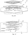
- FIGs 2A , 2B, 2C illustrate, in perspective view, a particular example of a multi-layer antenna arrangement 10 as illustrated in FIG 1 .
- the multi-layer antenna arrangement 10 has isolated first and second operational bandwidths 100 1 , 100 2 as illustrated in FIG 3A .
- the multi-layer antenna arrangement 10 comprises, in order:
- the multi-layer antenna arrangement 10 uses a ground plane 90.
- the fourth looped patch antenna element 24 in the fourth layer 34 is the looped patch antenna element nearest the ground plane.
- the multi-layer antenna arrangement 10 comprises the ground plane 90 in a sixth layer 36 in the ordered stack of layers.
- the fourth looped patch antenna element 24 in the fourth layer 34 and one of the second looped patch antenna element 22 in the second layer 32 and the first looped patch antenna element 21 in the first layer 31 are configured to form a first coupled pair 51 of looped patch antennas that resonate within the first operational bandwidth 100 1 .
- the third looped patch antenna element 23 in the third layer 33 and the other of the second looped patch antenna element 22 in the second layer 32 and the first looped patch antenna element 21 in the first layer 31 are configured to form a second coupled pair 52 of looped patch antennas that resonate within the second operational bandwidth 100 2
- the fourth looped patch antenna element 24 in the fourth layer 34 and the second looped patch antenna element 22 in the second layer 32 are configured to form a first coupled pair 51 of looped patch antennas that resonate within the first operational bandwidth 100 1 .
- the third looped patch antenna element 23 in the third layer 33 and the first looped patch antenna element 21 in the first layer 31 are configured to form a second coupled pair 52 of looped patch antennas that resonate within the second operational bandwidth 100 2 .
- the fourth looped patch antenna element 24 in the fourth layer 34 and the first looped patch antenna element 21 in the first layer 31 are configured to form a first coupled pair 51 of looped patch antennas that resonate within the first operational bandwidth 100 1 and the third looped patch antenna element 23 in the third layer 33 and the second looped patch antenna element 22 in the second layer are configured to form a second coupled pair 52 of looped patch antennas that resonate within the second operational bandwidth 100 2 .
- each of the looped patch antenna elements 21, 22, 23, 24 form a coupled pair 51, 52 of looped patch antennas. Not every pair 51, 52 are pairings of immediately physically adjacent looped patch antenna elements. There is at least one pair 51, 52 of looped patch antenna elements, where the looped patch antenna elements of the pair 51,52 are separated by at least one other looped patch antenna element.
- the multi-layer antenna arrangement 10 there can be 2N looped patch antenna elements forming N coupled pairs of looped patch antennas. Not every pair 51, 52 are pairings of immediately adjacent looped patch antenna elements. There can be at least one pair 51, 52 of looped patch antenna elements, where the looped patch antenna elements of the pair 51,52 are separated by one or more other looped patch antenna elements. Each pair of looped patch antennas provides a new operational bandwidth 100 n .
- the first operational bandwidth 100 1 is at a higher frequency than the second operational bandwidth 100 2 .
- the first operational bandwidth 100 1 is at a lower frequency than the second operational bandwidth 100 2 .
- the first operational bandwidth 100 1 is at a lower range of frequencies than the second operational bandwidth 100 2 .
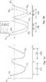
- FIG 3A illustrates a frequency response 70 of a reflection parameter S11 for the multi-layer antenna arrangement 10 when the first operational bandwidth 100 1 is at a lower frequency than the second operational bandwidth 100 2 .
- the reflection parameter S11 is less than a threshold value T in the first operational band 72 1 and the second operational band 72 2 and is more than a threshold value T in a stop band S.
- the stop band S splits a frequency range F into two distinct operational frequency bands - the first operational bandwidth 100 1 (F1), and the second operational bandwidth 100 2 (F2).
- the stop band S reduces cross-talk (interference) between the operational frequency bands 72 1 , 72 2 .
- the first operational bandwidth and the second operational bandwidth can both be a range that starts at a value greater than 24GHz.
- the operational bandwidths 100 are defined by a threshold -10 dB for the reflection parameter S11, then in some examples, the first operational band 72 1 has a first operational bandwidth 100 1 (F1) from 24.25 to 29.5 GHz and the second operational band 72 2 has a second operational bandwidth 100 2 (F2) from is 37 to 40 GHz.
- FIG 3B schematically illustrates a frequency response 50 of the reflection parameter S11 for each of the looped patch antenna elements 21, 22, 23, 24 that combine to form the multi-layer antenna arrangement 10 whose overall frequency response 70 has been discussed with reference to FIG 3A .
- the second looped patch antenna element 22 in the second layer 32 and the fourth looped patch antenna element 24 in the fourth layer 34 are configured to form the first coupled pair 51 of looped patch antennas that resonate within the first operational bandwidth 100 1 and the first looped patch antenna element 21 in the first layer 31 and the third looped patch antenna element 23 in the third layer 33 are configured to form the second coupled pair 52 of looped patch antennas that resonate within the second operational bandwidth 100 2 .
- Each looped patch antenna element 22, 24 of the first coupled pair 51 of looped patch antennas has a respective different electrical length that defines a respective different resonant frequency that lies within the first operational bandwidth 100 1 but outside the second operational bandwidth 100 2
- electrical length is a measurement of how long it takes electromagnetic waves to travel along a conductor that has resistance and reactance.
- the reactance may arise from capacitance and/or inductance and can be engineered.
- the first coupled pair 51 of looped patch antennas 22, 24 that resonate within the first operational bandwidth 100 1 have relatively similar but not identical electrical lengths.
- the second looped patch antenna element 22 in the second layer 32 has a second electrical length L2* which is related to the physical length L2, as illustrated in FIG 1 .
- the fourth looped patch antenna element 24 in the fourth layer 34 has a fourth electrical length L4* which is related to the physical length L4, as illustrated in FIG 1 .
- L2* L4* + ⁇ 1.
- the second looped patch antenna element 22 has a frequency response 50 2 of the reflection parameter S11.
- a fundamental mode of the second looped patch antenna element 22 is responsible for a second resonance mode 52 2 that has a resonant wavelength that is dependent on the electrical length L2* of the second looped patch antenna element 22.
- the resonant frequency RF 2 illustrated in FIG 3B is determined by the resonant wavelength.
- the fourth looped patch antenna element 24 has a frequency response 50 4 of the reflection parameter S11.
- a fundamental mode of the fourth looped patch antenna element 24 is responsible for a fourth resonance mode 52 4 that has a resonant wavelength that is dependent upon the electrical length L4* of the fourth looped patch antenna element 24.
- the resonant frequency RF 4 illustrated in FIG 3B is determined by the resonant wavelength.
- Each of the resonant modes 52 2 , 52 4 for the first coupled pair 51 of looped patch antennas 22, 24 has an associated operational frequency band.
- the associated operational frequency bands of the multiple resonant modes 52 2 , 52 4 overlap. The overlap is sufficient to define a combined operational frequency band 72 1 , as illustrated in FIG 3A , that has the first operational bandwidth 100 1 (F1).
- Each looped patch antenna element 21, 23 of the second coupled pair 52 of looped patch antennas has a respective different electrical length that defines a respective different resonant frequency that lies within the second operational bandwidth 100 2 but outside the first operational bandwidth 100 1 .
- the second coupled pair 52 of looped patch antennas 21, 23 that resonate within the second operational bandwidth 100 2 have relatively similar but not identical electrical lengths.
- the first looped patch antenna element 21 in the first layer 31 has a first electrical length L1* which is related to the physical length L1, as illustrated in FIG 1 .
- the third looped patch antenna element 23 in the third layer 33 has a third electrical length L3* which is related to the physical length L3, as illustrated in FIG 1 .
- L1* L3* + ⁇ 2.
- the first looped patch antenna element 21 has a frequency response 50 1 of the reflection parameter S11.
- a fundamental mode of the first looped patch antenna element 21 is responsible for a first resonance mode 52 1 that has a resonant wavelength that is dependent upon the electrical length L1* of the first looped patch antenna element 21.
- the resonant frequency RF 1 illustrated in FIG 3B is determined by the resonant wavelength.
- the third looped patch antenna element 23 has a frequency response 50 3 of the reflection parameter S11.
- a fundamental mode of the third looped patch antenna element 23 is responsible for a third resonance mode 52 3 that has a resonant wavelength that is dependent upon the electrical length L3* of the third looped patch antenna element 23.
- the resonant frequency RF 3 illustrated in FIG 3B is determined by the resonant wavelength.
- a fundamental mode, for example a dipole mode, of a looped patch antenna element is responsible for the resonance mode 52 n that has a resonant wavelength that is dependent upon, for example twice, the electrical length Ln* of the looped patch antenna element.
- the resonance of a looped patch antenna element when configured as a square ring patch antenna can, for example, be defined by the ratio of the physical length (L) of the ring and the equivalent physical length of the square central aperture 64. If one considers a virtual line passing through a center of the aperture 64, then the length of the looped patch antenna element is the distance along this line between the outer edges 68 and the length of the square central aperture 64 is the distance along this line between the inner edges 66. The distance between the inner edges 66 along the line is equal to the physical length minus the widths of looped patch antenna element along the line, that is minus the sum of the distances along the line between adjacent inner and outer edges 66, 68. In this example, the resonant wavelength of the looped patch antenna element is dependent upon multiple dimensions (length and width; length and aperture size) of the looped patch antenna element.
- the widths of the looped patch antenna element is constant. However, in other examples it may vary. In a dual polarized scenario the structure should be symmetric. In a single polarized structure width may change on different sides.
- Each of the resonant modes 52 1 , 52 3 for the second coupled pair 52 of looped patch antennas 21, 23 has an associated operational frequency band.
- the associated operational frequency bands of the multiple resonant modes 52 1 , 52 3 overlap. The overlap is sufficient to define a combined operational frequency band 72 2 , as illustrated in FIG 3A , that has the second operational bandwidth 100 2 (F2).
- the first coupled pair 51 of looped patch antennas 22, 24 that resonate within the first operational bandwidth 100 1 and second coupled pair 52 of looped patch antennas 21, 23 that resonate within the second operational bandwidth 100 2 have relatively different electrical lengths, sufficient to cause isolation between the first operational bandwidth 100 1 (F1) and the second operational bandwidth 100 2 (F2).
- the difference between the electrical lengths L2, L4 of the first coupled pair 51 of looped patch antennas 22, 24 that resonate within the first operational bandwidth 100 1 is greater than the difference between the electrical lengths L1, L3 of the second coupled pair 52 of looped patch antennas 21, 23 that resonate within the second operational bandwidth 100 2 .
- This will be necessary, if for example, the first operational bandwidth 100 1 and the second operational bandwidth 100 2 are to have a similar frequency range.
- the looped patch antenna elements of the first coupled pair 51 of looped patch antennas have axes 60 of rotational symmetry that are aligned and the looped patch antenna elements of the second coupled pair 52 of looped patch antennas have axes 60 of rotational symmetry that are aligned.
- the looped patch antenna elements of the first coupled pair 51 of looped patch antennas and the looped patch antenna elements of the second coupled pair 52 of looped patch antennas have a common shared axis 60 of rotational symmetry.
- the rotational symmetry is 90° rotational symmetry.
- An axes of n-fold rotational symmetry is a vector about which a looped patch antenna can be rotated by 360°/n, without any apparent change to the orientation of the looped patch antenna.
- the looped patch antenna elements are square and have 4-fold rotational symmetry in other examples they may be triangular (3-fold rotational symmetry) or rectangular (2-fold rotational symmetry).
- FIG 4 illustrates an example of a looped patch antenna element.
- the example it is labelled as the first looped patch antenna element 21.
- FIG 4 also illustrates features that are shared between the first, second, third, fourth looped patch antenna elements 21, 22, 23, 24.
- FIG 4 is a top plan view.
- FIGs 5A and 5B are cross-sectional views along the lines XX and YY of FIG 4 , respectively.
- the looped patch antenna 21 comprises a continuous conductor 62 that forms a closed planar loop around an inner aperture 64.
- the looped patch antenna 21 can also be called a ring patch, although this does not necessarily imply a particular shape.
- the looped patch antennas of the first and second coupled pairs 51, 52 of looped patch antennas are each a loop of constant width W.
- the respective first, second, third, fourth looped patch antenna elements 21, 22, 23, 24 can each have a different respective width W1, W2, W3, W4.
- the looped patch antennas of the first and second coupled pairs 51, 52 of looped patch antennas are each a loop of length dimension L.
- the respective first, second, third, fourth looped patch antenna elements 21, 22, 23, 24 can each have a different respective length L1, L2, L3, L4.
- the looped patch antennas of the first and second coupled pairs 51, 52 of looped patch antennas can each be a square planar loop of conductive material 62 aligned on the same axis 60.
- the square has a side of length L.
- the conductor 62 defining the looped patch antenna element has an inner edge 66 that circumscribes an aperture 64 and an exterior edge 68.
- the size of the aperture 64 can, in some examples, be several times wider than the width W.
- the looped patch antennas of the first and second coupled pairs 51, 52 of looped patch antennas are each at a height H above a ground plane 90.
- the respective first, second, third, fourth looped patch antenna elements 21, 22, 23, 24 can each have a different respective heights H1, H2, H3, H4.
- the distance separating the first looped patch antenna 21 and the second looped patch antenna 22 (H1-H2) is less than the distance separating the first coupled pair 51 of looped patch antennas and less than the distance separating the second coupled pair 52 of looped patch antennas.
- the distance separating the first looped patch antenna 21 and the second looped patch antenna 22 (H1-H2) is less than the distance (H2-H4) separating the first coupled pair 51 of looped patch antennas 22, 24 and less than the distance (H1-H3) separating the second coupled pair 52 of looped patch antennas 21, 23.
- the distance separating the first looped patch antenna 21 and the second looped patch antenna 22 (H1-H2) is less than the distance (H1-H4) separating the first coupled pair 51 of looped patch antennas 21, 24 and less than the distance (H2-H3) separating the second coupled pair 52 of looped patch antennas 22, 23.
- the first, second, third, fourth looped patch antenna elements 21, 22, 23, 24 can be arranged to differ from each other in dimensional parameters, for example, one of more of: length L, width W, height H.
- each FIG illustrates a multi-layer antenna arrangement 10 that uses a different dual polarized feed arrangement 40.
- the feed arrangement 40 is a differential feed arrangement. It comprises two pairs of differential feeds 42. There is a pair of microstrip feeds 42 for each one of two orthogonal polarizations. Each feed 42 can be a proximity coupled L probe.
- the pair of feeds 42A provide a first polarized, differential feed.
- the pair of feeds 42B provide a second polarized, differential feed.
- the feed arrangement 40 is a single ended feed. It comprises two feeds 42. There is a microstrip feed 42 for each one of two orthogonal polarizations. Each feed 42 can be a proximity coupled L probe.
- the feed 42A provides a first polarized single ended feed.
- the feed 42B provides a second polarized, single ended feed.
- the feed arrangement 40 is an aperture couple feed. Instead of providing a microstrip feed, an aperture 44 in a conductive ground plane is provided according in Babinet's principle.
- FIGs 2A , 2B, 2C illustrate dual -polarized feeds
- the feeds may be used as single polarization feeds or may be adapted to operate as single polarization feeds.
- Fig 6 illustrates an example of the multi-layer antenna arrangement 10 as previously described.
- the first, second, third, fourth, fifth and sixth layers 31, 32, 33, 34, 35, 36 are integrated as a single component 120.
- the single component 120 can, in some examples, be a substrate 122 where the first, second, third, fourth, fifth and sixth layers 31, 32, 33, 34, 35, 36 are stacked layers within a common substrate 122.
- the substrate 122 is a substrate of a transceiver circuit board.
- the looped patch antenna elements 21, 22, 23, 24 can be printed conductive strips.
- one or more but not all of the first, second, third, fourth, fifth and sixth layers 31, 32, 33, 34, 35, 36 are part of a first component, for example an antenna circuit board and the other ones of the first, second, third, fourth, fifth and sixth layers 31, 32, 33, 34, 35, 36 are part of a second component, for example a transceiver circuit board.
- Different materials with different dielectric constant ( ⁇ r) values can be used between the first, second, third, fourth, fifth and sixth layers 31, 32, 33, 34, 35, 36. For example, if higher ⁇ r is used, then the stacked structure of one or more but not all of the first, second, third, fourth looped patch antenna elements 21, 22, 23, 24 is more compact compared with a lower ⁇ r stack.
- patch antenna elements 21, 22, 23, 24 are paired to create two pairs that have respective different operational bandwidths.
- 2M patch antenna elements can be paired to create M pairs that have respective M different operational bandwidths.
- the antenna arrangement 10 can be configured as a filtenna.
- the antenna structure provides not just antenna functionality but also filtering functionality.
- FIG 7 illustrates an example of an electronic communications device 200, for example, a transceiver system 200, comprising the multi-layer antenna arrangement 10.
- the communications device 200 comprises a receiver system and a transmitter system.
- the multi-layer antenna arrangement 10 is directly connected to amplification circuitry 202 without an intervening band stop filter component.
- the absence of the band stop filter component is indicated by reference 206 in the receiver system and the transmitter system.
- the communication device 200 may, for example, be used in a base station or a mobile station. It may, for example, be suitable for, and not limited to, use in 5G telecommunications.
- the receiver system is present but the transmitter system is not.
- the transmitter system is present but the receiver system is not.
- the communication device 200 and/or the multi-layer antenna arrangement 10 have several advantages including compact size, good inter-band rejection, a constant radiation pattern shape for dual band and dual polarization, ease of fabrication and freedom of resonator design by adjusting the geometry of four individual looped patch antenna elements 21, 22, 23, 24.
- a radio module and/or a complete radio unit can comprise the multi-layer antenna arrangement 10 and associated transmitter and/or receiver circuitry.
- the multi-layer antenna arrangement 10 can be used to form an antenna array. Multiple ones of the multi-layer antenna arrangement 10 can be used to form an antenna array.
- An operational resonant mode is a frequency range over which an antenna can efficiently operate.
- An operational resonant mode may be defined as where the absolute value of the return loss S11 of the antenna arrangement is greater than an operational threshold T.
- the antenna arrangement 10 may be configured to operate in a plurality of operational resonant frequency bands.
- the operational frequency bands may include (but are not limited to) Long Term Evolution (LTE) (US) (734 to 746 MHz and 869 to 894 MHz), Long Term Evolution (LTE) (rest of the world) (791 to 821 MHz and 925 to 960 MHz), amplitude modulation (AM) radio (0.535-1.705 MHz); frequency modulation (FM) radio (76-108 MHz); Bluetooth (2400-2483.5 MHz); wireless local area network (WLAN) (2400-2483.5 MHz); hiper local area network (HiperLAN) (5150-5850 MHz); global positioning system (GPS) (1570.42-1580.42 MHz); US - Global system for mobile communications (US-GSM) 850 (824-894 MHz) and 1900 (1850 - 1990 MHz); European global system for mobile communications (EGSM) 900 (880-960 MHz) and 1800 (1710 - 1880 MHz); European wideband code
- module' refers to a unit or apparatus that excludes certain parts/components that would be added by an end manufacturer or a user.
- the antenna arrangement 10 can be a module.
- the above described examples find application as enabling components of: satellite communications and wireless industrial systems (industrial internet); automotive systems; telecommunication systems; electronic systems including consumer electronic products; distributed computing systems; media systems for generating or rendering media content including audio, visual and audio visual content and mixed, mediated, virtual and/or augmented reality; personal systems including personal health systems or personal fitness systems; navigation systems; user interfaces also known as human machine interfaces; networks including cellular, non-cellular, and optical networks; ad-hoc networks; the internet; the internet of things; virtualized networks; and related software and services.
- satellite communications and wireless industrial systems industrial internet
- automotive systems telecommunication systems
- electronic systems including consumer electronic products
- distributed computing systems media systems for generating or rendering media content including audio, visual and audio visual content and mixed, mediated, virtual and/or augmented reality
- personal systems including personal health systems or personal fitness systems
- navigation systems user interfaces also known as human machine interfaces
- networks including cellular, non-cellular, and optical networks
- ad-hoc networks the internet; the internet of things; virtualized
- a property of the instance can be a property of only that instance or a property of the class or a property of a sub-class of the class that includes some but not all of the instances in the class. It is therefore implicitly disclosed that a feature described with reference to one example but not with reference to another example, can where possible be used in that other example as part of a working combination but does not necessarily have to be used in that other example.
- 'a' or 'the' is used in this document with an inclusive not an exclusive meaning. That is any reference to X comprising a/the Y indicates that X may comprise only one Y or may comprise more than one Y unless the context clearly indicates the contrary. If it is intended to use 'a' or 'the' with an exclusive meaning then it will be made clear in the context. In some circumstances the use of 'at least one' or 'one or more' may be used to emphasis an inclusive meaning but the absence of these terms should not be taken to infer and exclusive meaning.
- the presence of a feature (or combination of features) in a claim is a reference to that feature or (combination of features) itself and also to features that achieve substantially the same technical effect (equivalent features).
- the equivalent features include, for example, features that are variants and achieve substantially the same result in substantially the same way.
- the equivalent features include, for example, features that perform substantially the same function, in substantially the same way to achieve substantially the same result.
Landscapes
- Physics & Mathematics (AREA)
- Electromagnetism (AREA)
- Waveguide Aerials (AREA)
Abstract
Description
- Embodiments of the present invention relate to a multi-band antenna arrangement. Some embodiments of the present disclosure relate to a multi-band antenna arrangement suitable for use in 5G and other telecommunication systems.
- Telecommunication standards specify operational frequency bands. It is therefore desirable for a transceiver to be multi-band and operate in multiple different operational frequency bands.
- While, in some examples, it may be possible to use an antenna arrangement that has a single wide operational bandwidth that covers simultaneously multiple different operational frequency bands, this can be undesirable as there can then be insufficient isolation between communications in the different operational frequency bands causing interference.
- According to various, but not necessarily all, embodiments there is provided
a multi-layer antenna arrangement having isolated first and second operational bandwidths, the antenna arrangement comprising, in order: - a first looped patch antenna element in a first layer;
- a second looped patch antenna element in a second layer;
- a third looped patch antenna element in a third layer;
- a fourth looped patch antenna element in a fourth layer; and
- a conductive feed arrangement in a fifth layer,
- In some but not necessarily all examples, the first, second, third, fourth and fifth layers are integrated as a single component.
- In some but not necessarily all examples, the first looped patch antenna element in the first layer is a first printed conductive microstrip; the second looped patch antenna element in the second layer is a second printed conductive microstrip; the third looped patch antenna element in the third layer is a third printed conductive microstrip and the fourth looped patch antenna element in the fourth layer is a fourth printed conductive microstrip.
- In some but not necessarily all examples, the first looped patch antenna element, the second looped patch antenna element, the third looped patch antenna element, and the fourth looped patch antenna element are integral components of a transceiver circuit board.
- In some but not necessarily all examples, the first looped patch antenna element in the first layer and the third looped patch antenna element in the third layer are configured to form the first coupled pair of looped patch antennas that resonates within the first operational bandwidth and the second looped patch antenna element in the second layer and the fourth looped patch antenna element in the fourth layer are configured to form the second coupled pair of looped patch antennas that resonate within the second operational bandwidth.
- In some but not necessarily all examples, the first coupled pair of looped patch antennas that resonate within the first operational bandwidth have relatively similar but not identical electrical lengths providing the first operational bandwidth and wherein the second coupled pair of looped patch antennas that resonate within the second operational bandwidth have relatively similar but not identical electrical lengths providing the second operational bandwidth and wherein the first coupled pair of looped patch antennas that resonate within the first operational bandwidth and the second coupled pair of looped patch antennas that resonate within the second operational bandwidth have relatively different electrical lengths providing isolation of the first and second operational bandwidths.
- In some but not necessarily all examples, each looped patch antenna of the first coupled pair of looped patch antennas has a respective electrical length that defines a respective different resonant frequency that lies within the first operational bandwidth, and each looped patch antenna of the second coupled pair of looped patch antennas has a respective electrical length that defines a respective different resonant frequency that lies within the second operational bandwidth.
- In some but not necessarily all examples, the looped patch antennas of the first coupled pair of looped patch antennas have axes of rotational symmetry that are aligned and the looped patch antennas of the second coupled pair of looped patch antennas have axes of rotational symmetry that are aligned.
- In some but not necessarily all examples, each looped patch antenna element comprises a continuous conductor that forms a closed loop around an inner aperture.
- In some but not necessarily all examples, the continuous conductor of each looped patch antenna has a constant width.
- In some but not necessarily all examples, a distance separating the first looped patch antenna element in the first layer and the second looped patch antenna element in the second layer is less than a distance separating the first coupled pair of looped patch antennas and less than a distance separating the second coupled pair of looped patch antennas.
- In some but not necessarily all examples, the conductive feed arrangement is configured for dual polarization.
- In some but not necessarily all examples, the first operational bandwidth and the second operational bandwidth are each a non-overlapping range starting at a frequency value greater than 24GHz.
- In some but not necessarily all examples,, an electronic communications device comprises the multi-layer antenna arrangement. In some but not necessarily all examples, the multi-layer antenna arrangement is directly connected to amplification circuitry without an intervening band stop filter component.
- According to various, but not necessarily all, embodiments there is provided examples as claimed in the appended claims.
- Some example embodiments will now be described with reference to the accompanying drawings in which:
-
FIG 1 shows an example of the subject-matter described herein; -
FIG 2A shows an example of the subject-matter described herein; -
FIG 2B shows an example of the subject-matter described herein; -
FIG 2C shows an example of the subject-matter described herein; -
FIG 3A shows an example of the subject-matter described herein; -
FIG 3B shows an example of the subject-matter described herein; -
FIG 4 shows an example of the subject-matter described herein; -
FIG 5A shows an example of the subject-matter described herein; -
FIG 5B shows an example of the subject-matter described herein; -
FIG 6 shows an example of the subject-matter described herein; and -
FIG 7 shows an example of the subject-matter described herein; -
FIG 1 illustrates in side view, a cross-section through a generic example ofmulti-layer antenna arrangement 10. Each ofFIGs 2A ,2B, 2C illustrate, in perspective view, a particular example of amulti-layer antenna arrangement 10 as illustrated inFIG 1 . Themulti-layer antenna arrangement 10 has isolated first and second operational bandwidths 1001, 1002 as illustrated inFIG 3A . - The
multi-layer antenna arrangement 10 comprises, in order: - a first looped
patch antenna element 21 in afirst layer 31; - a second looped
patch antenna element 22 in asecond layer 32; - a third looped
patch antenna element 23 in athird layer 33; - a fourth looped
patch antenna element 24 in afourth layer 34; and - one or more
conductive feeds 40 in afifth layer 35. - In at least some examples, the
multi-layer antenna arrangement 10 uses aground plane 90. The fourth loopedpatch antenna element 24 in thefourth layer 34 is the looped patch antenna element nearest the ground plane. In some but not necessarily all examples, for example as illustrated inFIGs 2A ,2B, 2C , themulti-layer antenna arrangement 10 comprises theground plane 90 in asixth layer 36 in the ordered stack of layers. - The fourth looped
patch antenna element 24 in thefourth layer 34 and one of the second loopedpatch antenna element 22 in thesecond layer 32 and the first loopedpatch antenna element 21 in thefirst layer 31 are configured to form a first coupledpair 51 of looped patch antennas that resonate within the first operational bandwidth 1001. - The third looped
patch antenna element 23 in thethird layer 33 and the other of the second loopedpatch antenna element 22 in thesecond layer 32 and the first loopedpatch antenna element 21 in thefirst layer 31 are configured to form a second coupledpair 52 of looped patch antennas that resonate within the second operational bandwidth 1002 - In the example (i) in
FIG 1 , the fourth loopedpatch antenna element 24 in thefourth layer 34 and the second loopedpatch antenna element 22 in thesecond layer 32 are configured to form a first coupledpair 51 of looped patch antennas that resonate within the first operational bandwidth 1001. and the third loopedpatch antenna element 23 in thethird layer 33 and the first loopedpatch antenna element 21 in thefirst layer 31 are configured to form a second coupledpair 52 of looped patch antennas that resonate within the second operational bandwidth 1002. - In the example (ii) in
FIG 1 , the fourth loopedpatch antenna element 24 in thefourth layer 34 and the first loopedpatch antenna element 21 in thefirst layer 31 are configured to form a first coupledpair 51 of looped patch antennas that resonate within the first operational bandwidth 1001 and the third loopedpatch antenna element 23 in thethird layer 33 and the second loopedpatch antenna element 22 in the second layer are configured to form a second coupledpair 52 of looped patch antennas that resonate within the second operational bandwidth 1002. - In the examples (i) and (ii) in
FIG 1 , each of the loopedpatch antenna elements pair pair pair pair - In other examples of the
multi-layer antenna arrangement 10 there can be 2N looped patch antenna elements forming N coupled pairs of looped patch antennas. Not everypair pair pair - In some but not necessarily all examples, the first operational bandwidth 1001 is at a higher frequency than the second operational bandwidth 1002.
- In some but not necessarily all examples, the first operational bandwidth 1001 is at a lower frequency than the second operational bandwidth 1002.
- In the example of
FIG 3A , the first operational bandwidth 1001 is at a lower range of frequencies than the second operational bandwidth 1002. -
FIG 3A illustrates afrequency response 70 of a reflection parameter S11 for themulti-layer antenna arrangement 10 when the first operational bandwidth 1001 is at a lower frequency than the second operational bandwidth 1002. - The reflection parameter S11 is less than a threshold value T in the first operational band 721 and the second operational band 722 and is more than a threshold value T in a stop band S. The stop band S splits a frequency range F into two distinct operational frequency bands - the first operational bandwidth 1001 (F1), and the second operational bandwidth 1002 (F2). The stop band S reduces cross-talk (interference) between the operational frequency bands 721, 722.
- The first operational bandwidth and the second operational bandwidth can both be a range that starts at a value greater than 24GHz. For example, if the operational bandwidths 100 are defined by a threshold -10 dB for the reflection parameter S11, then in some examples, the first operational band 721 has a first operational bandwidth 1001 (F1) from 24.25 to 29.5 GHz and the second operational band 722 has a second operational bandwidth 1002 (F2) from is 37 to 40 GHz.
-
FIG 3B schematically illustrates a frequency response 50 of the reflection parameter S11 for each of the loopedpatch antenna elements multi-layer antenna arrangement 10 whoseoverall frequency response 70 has been discussed with reference toFIG 3A . - For the purpose of the following example, the second looped
patch antenna element 22 in thesecond layer 32 and the fourth loopedpatch antenna element 24 in thefourth layer 34 are configured to form the first coupledpair 51 of looped patch antennas that resonate within the first operational bandwidth 1001 and the first loopedpatch antenna element 21 in thefirst layer 31 and the third loopedpatch antenna element 23 in thethird layer 33 are configured to form the second coupledpair 52 of looped patch antennas that resonate within the second operational bandwidth 1002.This corresponds to example (i) inFIG 1 . - Each looped
patch antenna element pair 51 of looped patch antennas has a respective different electrical length that defines a respective different resonant frequency that lies within the first operational bandwidth 1001 but outside the second operational bandwidth 1002 - Whereas physical length is a measurement of how long it takes electromagnetic waves to travel along a conductor that is resistive only; electrical length is a measurement of how long it takes electromagnetic waves to travel along a conductor that has resistance and reactance. The reactance may arise from capacitance and/or inductance and can be engineered.
- The first coupled
pair 51 of loopedpatch antennas patch antenna element 22 in thesecond layer 32 has a second electrical length L2* which is related to the physical length L2, as illustrated inFIG 1 . The fourth loopedpatch antenna element 24 in thefourth layer 34 has a fourth electrical length L4* which is related to the physical length L4, as illustrated inFIG 1 . In this example, L2*=L4* +δ1. - The second looped
patch antenna element 22 has a frequency response 502 of the reflection parameter S11. A fundamental mode of the second loopedpatch antenna element 22 is responsible for asecond resonance mode 522 that has a resonant wavelength that is dependent on the electrical length L2* of the second loopedpatch antenna element 22. The resonant frequency RF2 illustrated inFIG 3B is determined by the resonant wavelength. - The fourth looped
patch antenna element 24 has a frequency response 504 of the reflection parameter S11. A fundamental mode of the fourth loopedpatch antenna element 24 is responsible for afourth resonance mode 524 that has a resonant wavelength that is dependent upon the electrical length L4* of the fourth loopedpatch antenna element 24. The resonant frequency RF4 illustrated inFIG 3B is determined by the resonant wavelength. - Each of the
resonant modes pair 51 of loopedpatch antennas resonant modes FIG 3A , that has the first operational bandwidth 1001 (F1). - Each looped
patch antenna element pair 52 of looped patch antennas has a respective different electrical length that defines a respective different resonant frequency that lies within the second operational bandwidth 1002 but outside the first operational bandwidth 1001. - The second coupled
pair 52 of loopedpatch antennas patch antenna element 21 in thefirst layer 31 has a first electrical length L1* which is related to the physical length L1, as illustrated inFIG 1 . The third loopedpatch antenna element 23 in thethird layer 33 has a third electrical length L3* which is related to the physical length L3, as illustrated inFIG 1 . In this example, L1*=L3* +δ2. - The first looped
patch antenna element 21 has a frequency response 501 of the reflection parameter S11. A fundamental mode of the first loopedpatch antenna element 21 is responsible for afirst resonance mode 521 that has a resonant wavelength that is dependent upon the electrical length L1* of the first loopedpatch antenna element 21. The resonant frequency RF1 illustrated inFIG 3B is determined by the resonant wavelength. - The third looped
patch antenna element 23 has a frequency response 503 of the reflection parameter S11. A fundamental mode of the third loopedpatch antenna element 23 is responsible for athird resonance mode 523 that has a resonant wavelength that is dependent upon the electrical length L3* of the third loopedpatch antenna element 23. The resonant frequency RF3 illustrated inFIG 3B is determined by the resonant wavelength. - In the above examples, a fundamental mode, for example a dipole mode, of a looped patch antenna element is responsible for the
resonance mode 52n that has a resonant wavelength that is dependent upon, for example twice, the electrical length Ln* of the looped patch antenna element. - The resonance of a looped patch antenna element when configured as a square ring patch antenna can, for example, be defined by the ratio of the physical length (L) of the ring and the equivalent physical length of the square
central aperture 64. If one considers a virtual line passing through a center of theaperture 64, then the length of the looped patch antenna element is the distance along this line between theouter edges 68 and the length of the squarecentral aperture 64 is the distance along this line between the inner edges 66. The distance between theinner edges 66 along the line is equal to the physical length minus the widths of looped patch antenna element along the line, that is minus the sum of the distances along the line between adjacent inner andouter edges - In at least some examples the widths of the looped patch antenna element is constant. However, in other examples it may vary. In a dual polarized scenario the structure should be symmetric. In a single polarized structure width may change on different sides.
- Each of the
resonant modes pair 52 of loopedpatch antennas resonant modes FIG 3A , that has the second operational bandwidth 1002 (F2). - In some but not necessarily all examples, the first coupled
pair 51 of loopedpatch antennas pair 52 of loopedpatch antennas - Where the first operational bandwidth 1001 is at lower frequencies (longer wavelengths) than the second operational bandwidth 1002, then the difference between the electrical lengths L2, L4 of the first coupled
pair 51 of loopedpatch antennas pair 52 of loopedpatch antennas - Referring to
FIGs 1, 2A ,2B, 2C andFIG 4 the looped patch antenna elements of the first coupledpair 51 of looped patch antennas haveaxes 60 of rotational symmetry that are aligned and the looped patch antenna elements of the second coupledpair 52 of looped patch antennas haveaxes 60 of rotational symmetry that are aligned. - As illustrated in
FIGs 1, 2A ,2B, 2C in at least some examples, the looped patch antenna elements of the first coupledpair 51 of looped patch antennas and the looped patch antenna elements of the second coupledpair 52 of looped patch antennas have a common sharedaxis 60 of rotational symmetry. In this example, but not necessarily all examples, the rotational symmetry is 90° rotational symmetry. - An axes of n-fold rotational symmetry is a vector about which a looped patch antenna can be rotated by 360°/n, without any apparent change to the orientation of the looped patch antenna.
- Although in these FIGs, the looped patch antenna elements are square and have 4-fold rotational symmetry in other examples they may be triangular (3-fold rotational symmetry) or rectangular (2-fold rotational symmetry).
-
FIG 4 illustrates an example of a looped patch antenna element. In the example it is labelled as the first loopedpatch antenna element 21. However, it also illustrates features that are shared between the first, second, third, fourth loopedpatch antenna elements FIG 4 is a top plan view.FIGs 5A and 5B are cross-sectional views along the lines XX and YY ofFIG 4 , respectively. - The looped
patch antenna 21 comprises acontinuous conductor 62 that forms a closed planar loop around aninner aperture 64. The loopedpatch antenna 21 can also be called a ring patch, although this does not necessarily imply a particular shape. - In the example illustrated, the looped patch antennas of the first and second coupled pairs 51, 52 of looped patch antennas are each a loop of constant width W. The respective first, second, third, fourth looped
patch antenna elements - In the example illustrated, the looped patch antennas of the first and second coupled pairs 51, 52 of looped patch antennas are each a loop of length dimension L. The respective first, second, third, fourth looped
patch antenna elements - The looped patch antennas of the first and second coupled pairs 51, 52 of looped patch antennas can each be a square planar loop of
conductive material 62 aligned on thesame axis 60. The square has a side of length L. - The
conductor 62 defining the looped patch antenna element has aninner edge 66 that circumscribes anaperture 64 and anexterior edge 68. The size of theaperture 64 can, in some examples, be several times wider than the width W. - As illustrated in
FIG 5A and 5B , the looped patch antennas of the first and second coupled pairs 51, 52 of looped patch antennas are each at a height H above aground plane 90. The respective first, second, third, fourth loopedpatch antenna elements - In some examples, the distance separating the first looped
patch antenna 21 and the second looped patch antenna 22 (H1-H2) is less than the distance separating the first coupledpair 51 of looped patch antennas and less than the distance separating the second coupledpair 52 of looped patch antennas. - Considering the example (i) in
FIG 1 , the distance separating the first loopedpatch antenna 21 and the second looped patch antenna 22 (H1-H2) is less than the distance (H2-H4) separating the first coupledpair 51 of loopedpatch antennas pair 52 of loopedpatch antennas - Considering the example (ii) in
FIG 1 , the distance separating the first loopedpatch antenna 21 and the second looped patch antenna 22 (H1-H2) is less than the distance (H1-H4) separating the first coupledpair 51 of loopedpatch antennas pair 52 of loopedpatch antennas - The first, second, third, fourth looped
patch antenna elements multi-layer antenna arrangement 10. - Referring back to the examples of
FIGs 2A ,2B, 2C , each FIG illustrates amulti-layer antenna arrangement 10 that uses a different dualpolarized feed arrangement 40. - In
FIG 2A , thefeed arrangement 40 is a differential feed arrangement. It comprises two pairs of differential feeds 42. There is a pair of microstrip feeds 42 for each one of two orthogonal polarizations. Each feed 42 can be a proximity coupled L probe. The pair offeeds 42A provide a first polarized, differential feed. The pair offeeds 42B provide a second polarized, differential feed. - In
FIG 2B , thefeed arrangement 40 is a single ended feed. It comprises two feeds 42. There is a microstrip feed 42 for each one of two orthogonal polarizations. Each feed 42 can be a proximity coupled L probe. Thefeed 42A provides a first polarized single ended feed. Thefeed 42B provides a second polarized, single ended feed. - In
FIG 2C , thefeed arrangement 40 is an aperture couple feed. Instead of providing a microstrip feed, anaperture 44 in a conductive ground plane is provided according in Babinet's principle. - Whereas
FIGs 2A ,2B, 2C illustrate dual -polarized feeds, in other examples the feeds may be used as single polarization feeds or may be adapted to operate as single polarization feeds. -
Fig 6 illustrates an example of themulti-layer antenna arrangement 10 as previously described. In this example, the first, second, third, fourth, fifth andsixth layers single component 120. - The
single component 120 can, in some examples, be asubstrate 122 where the first, second, third, fourth, fifth andsixth layers common substrate 122. - In some but not necessarily all examples, the
substrate 122 is a substrate of a transceiver circuit board. - The looped
patch antenna elements FIG 6 ) can be printed conductive strips. - Standard PCB manufacturing techniques can be used.
- In some but not necessarily all examples, one or more but not all of the first, second, third, fourth, fifth and
sixth layers sixth layers - Different materials with different dielectric constant (εr) values can be used between the first, second, third, fourth, fifth and
sixth layers patch antenna elements - In the preceding examples, four
patch antenna elements - The
antenna arrangement 10 can be configured as a filtenna. The antenna structure provides not just antenna functionality but also filtering functionality.
FIG 7 illustrates an example of anelectronic communications device 200, for example, atransceiver system 200, comprising themulti-layer antenna arrangement 10. Thecommunications device 200 comprises a receiver system and a transmitter system. In this example, themulti-layer antenna arrangement 10 is directly connected toamplification circuitry 202 without an intervening band stop filter component. The absence of the band stop filter component is indicated byreference 206 in the receiver system and the transmitter system. - The
communication device 200 may, for example, be used in a base station or a mobile station. It may, for example, be suitable for, and not limited to, use in 5G telecommunications. - In a receiver only implementation, the receiver system is present but the transmitter system is not. In a transmitter only implementation, the transmitter system is present but the receiver system is not.
- The
communication device 200 and/or themulti-layer antenna arrangement 10 have several advantages including compact size, good inter-band rejection, a constant radiation pattern shape for dual band and dual polarization, ease of fabrication and freedom of resonator design by adjusting the geometry of four individual loopedpatch antenna elements - A radio module and/or a complete radio unit can comprise the
multi-layer antenna arrangement 10 and associated transmitter and/or receiver circuitry. - The
multi-layer antenna arrangement 10 can be used to form an antenna array. Multiple ones of themulti-layer antenna arrangement 10 can be used to form an antenna array. - Where a structural feature has been described, it may be replaced by means for performing one or more of the functions of the structural feature whether that function or those functions are explicitly or implicitly described.
- An operational resonant mode (operational band or bandwidth) is a frequency range over which an antenna can efficiently operate. An operational resonant mode (operational band) may be defined as where the absolute value of the return loss S11 of the antenna arrangement is greater than an operational threshold T.
- The
antenna arrangement 10 may be configured to operate in a plurality of operational resonant frequency bands. For example, the operational frequency bands may include (but are not limited to) Long Term Evolution (LTE) (US) (734 to 746 MHz and 869 to 894 MHz), Long Term Evolution (LTE) (rest of the world) (791 to 821 MHz and 925 to 960 MHz), amplitude modulation (AM) radio (0.535-1.705 MHz); frequency modulation (FM) radio (76-108 MHz); Bluetooth (2400-2483.5 MHz); wireless local area network (WLAN) (2400-2483.5 MHz); hiper local area network (HiperLAN) (5150-5850 MHz); global positioning system (GPS) (1570.42-1580.42 MHz); US - Global system for mobile communications (US-GSM) 850 (824-894 MHz) and 1900 (1850 - 1990 MHz); European global system for mobile communications (EGSM) 900 (880-960 MHz) and 1800 (1710 - 1880 MHz); European wideband code division multiple access (EU-WCDMA) 900 (880-960 MHz); personal communications network (PCN/DCS) 1800 (1710-1880 MHz); US wideband code division multiple access (US-WCDMA) 1700 (transmit: 1710 to 1755 MHz , receive: 2110 to 2155 MHz) and 1900 (1850-1990 MHz); wideband code division multiple access (WCDMA) 2100 (transmit: 1920-1980 MHz, receive: 2110-2180 MHz); personal communications service (PCS) 1900 (1850-1990 MHz); time division synchronous code division multiple access (TD-SCDMA) (1900 MHz to 1920 MHz, 2010 MHz to 2025 MHz), ultra wideband (UWB) Lower (3100-4900 MHz); UWB Upper (6000-10600 MHz); digital video broadcasting - handheld (DVB-H) (470-702 MHz); DVB-HUS (1670-1675 - As used here 'module' refers to a unit or apparatus that excludes certain parts/components that would be added by an end manufacturer or a user. The
antenna arrangement 10 can be a module. - The above described examples find application as enabling components of:
satellite communications and wireless industrial systems (industrial internet); automotive systems; telecommunication systems; electronic systems including consumer electronic products; distributed computing systems; media systems for generating or rendering media content including audio, visual and audio visual content and mixed, mediated, virtual and/or augmented reality; personal systems including personal health systems or personal fitness systems; navigation systems; user interfaces also known as human machine interfaces; networks including cellular, non-cellular, and optical networks; ad-hoc networks; the internet; the internet of things; virtualized networks; and related software and services. - The term 'comprise' is used in this document with an inclusive not an exclusive meaning. That is any reference to X comprising Y indicates that X may comprise only one Y or may comprise more than one Y. If it is intended to use 'comprise' with an exclusive meaning then it will be made clear in the context by referring to "comprising only one" or by using "consisting".
- In this description, reference has been made to various examples. The description of features or functions in relation to an example indicates that those features or functions are present in that example. The use of the term 'example' or 'for example' or 'can' or 'may' in the text denotes, whether explicitly stated or not, that such features or functions are present in at least the described example, whether described as an example or not, and that they can be, but are not necessarily, present in some of or all other examples. Thus 'example', 'for example', 'can' or 'may' refers to a particular instance in a class of examples. A property of the instance can be a property of only that instance or a property of the class or a property of a sub-class of the class that includes some but not all of the instances in the class. It is therefore implicitly disclosed that a feature described with reference to one example but not with reference to another example, can where possible be used in that other example as part of a working combination but does not necessarily have to be used in that other example.
- Although embodiments have been described in the preceding paragraphs with reference to various examples, it should be appreciated that modifications to the examples given can be made without departing from the scope of the claims.
- Features described in the preceding description may be used in combinations other than the combinations explicitly described above.
- Although functions have been described with reference to certain features, those functions may be performable by other features whether described or not.
- Although features have been described with reference to certain embodiments, those features may also be present in other embodiments whether described or not.
- The term 'a' or 'the' is used in this document with an inclusive not an exclusive meaning. That is any reference to X comprising a/the Y indicates that X may comprise only one Y or may comprise more than one Y unless the context clearly indicates the contrary. If it is intended to use 'a' or 'the' with an exclusive meaning then it will be made clear in the context. In some circumstances the use of 'at least one' or 'one or more' may be used to emphasis an inclusive meaning but the absence of these terms should not be taken to infer and exclusive meaning.
- The presence of a feature (or combination of features) in a claim is a reference to that feature or (combination of features) itself and also to features that achieve substantially the same technical effect (equivalent features). The equivalent features include, for example, features that are variants and achieve substantially the same result in substantially the same way. The equivalent features include, for example, features that perform substantially the same function, in substantially the same way to achieve substantially the same result.
- In this description, reference has been made to various examples using adjectives or adjectival phrases to describe characteristics of the examples. Such a description of a characteristic in relation to an example indicates that the characteristic is present in some examples exactly as described and is present in other examples substantially as described.
- Whilst endeavoring in the foregoing specification to draw attention to those features believed to be of importance it should be understood that the Applicant may seek protection via the claims in respect of any patentable feature or combination of features hereinbefore referred to and/or shown in the drawings whether or not emphasis has been placed thereon.
the fourth looped patch antenna element in the fourth layer and one of the second looped patch antenna element in the second layer and the first looped patch antenna element in the first layer are configured to form a first coupled pair of looped patch antennas that resonate within the first operational bandwidth and the third looped patch antenna element in the third layer and the other of the second looped patch antenna element in the second layer and the first looped patch antenna element in the first layer are configured to form a second coupled pair of looped patch antennas that resonate within the second operational bandwidth.
Claims (15)
- A multi-layer antenna arrangement having isolated first and second operational bandwidths, the antenna arrangement comprising, in order:a first looped patch antenna element in a first layer;a second looped patch antenna element in a second layer;a third looped patch antenna element in a third layer;a fourth looped patch antenna element in a fourth layer; anda conductive feed arrangement in a fifth layer,wherein
the fourth looped patch antenna element in the fourth layer and one of the second looped patch antenna element in the second layer and the first looped patch antenna element in the first layer are configured to form a first coupled pair of looped patch antennas that resonate within the first operational bandwidth and
the third looped patch antenna element in the third layer and the other of the second looped patch antenna element in the second layer and the first looped patch antenna element in the first layer are configured to form a second coupled pair of looped patch antennas that resonate within the second operational bandwidth. - A multi-layer antenna arrangement as claimed in claim 1, wherein the first, second, third, fourth and fifth layers are integrated as a single component.
- A multi-layer antenna arrangement as claimed in any preceding claim, wherein the first looped patch antenna element in the first layer is a first printed conductive microstrip; the second looped patch antenna element in the second layer is a second printed conductive microstrip; the third looped patch antenna element in the third layer is a third printed conductive microstrip and the fourth looped patch antenna element in the fourth layer is a fourth printed conductive microstrip.
- A multi-layer antenna arrangement as claimed in any preceding claim, wherein the first looped patch antenna element, the second looped patch antenna element, the third looped patch antenna element, and the fourth looped patch antenna element are integral components of a transceiver circuit board.
- A multi-layer antenna arrangement as claimed in any preceding claim, wherein the first looped patch antenna element in the first layer and the third looped patch antenna element in the third layer are configured to form the first coupled pair of looped patch antennas that resonates within the first operational bandwidth and the second looped patch antenna element in the second layer and the fourth looped patch antenna element in the fourth layer are configured to form the second coupled pair of looped patch antennas that resonate within the second operational bandwidth.
- A multi-layer antenna arrangement as claimed in any preceding claim, wherein the first coupled pair of looped patch antennas that resonate within the first operational bandwidth have relatively similar but not identical electrical lengths providing the first operational bandwidth and wherein the second coupled pair of looped patch antennas that resonate within the second operational bandwidth have relatively similar but not identical electrical lengths providing the second operational bandwidth and wherein the first coupled pair of looped patch antennas that resonate within the first operational bandwidth and the second coupled pair of looped patch antennas that resonate within the second operational bandwidth have relatively different electrical lengths providing isolation of the first and second operational bandwidths.
- A multi-layer antenna arrangement as claimed in any preceding claim, wherein each looped patch antenna of the first coupled pair of looped patch antennas has a respective electrical length that defines a respective different resonant frequency that lies within the first operational bandwidth, and each looped patch antenna of the second coupled pair of looped patch antennas has a respective electrical length that defines a respective different resonant frequency that lies within the second operational bandwidth.
- A multi-layer antenna arrangement as claimed in any preceding claim, wherein the looped patch antennas of the first coupled pair of looped patch antennas have axes of rotational symmetry that are aligned and the looped patch antennas of the second coupled pair of looped patch antennas have axes of rotational symmetry that are aligned.
- A multi-layer antenna arrangement as claimed in any preceding claim, wherein each looped patch antenna element comprises a continuous conductor that forms a closed loop around an inner aperture.
- A multi-layer antenna arrangement as claimed in claim 9, wherein the continuous conductor of each looped patch antenna has a constant width.
- A multi-layer antenna arrangement as claimed in any preceding claim, wherein a distance separating the first looped patch antenna element in the first layer and the second looped patch antenna element in the second layer is less than a distance separating the first coupled pair of looped patch antennas and less than a distance separating the second coupled pair of looped patch antennas.
- A multi-layer antenna arrangement as claimed in any preceding claim, wherein the conductive feed arrangement is configured for dual polarization.
- A multi-layer antenna arrangement as claimed in any preceding claim, wherein the first operational bandwidth and the second operational bandwidth are each a non-overlapping range starting at a frequency value greater than 24GHz.
- An electronic communications device comprising the multi-layer antenna arrangement as claimed in any preceding claim.
- An electronic communication device as claimed in claim 14, wherein the multi-layer antenna arrangement is configured as a filtenna and is directly connected to amplification circuitry without an intervening band stop filter component.
Priority Applications (1)
| Application Number | Priority Date | Filing Date | Title |
|---|---|---|---|
| EP19176293.9A EP3742552B1 (en) | 2019-05-23 | 2019-05-23 | A multi-band antenna arrangement |
Applications Claiming Priority (1)
| Application Number | Priority Date | Filing Date | Title |
|---|---|---|---|
| EP19176293.9A EP3742552B1 (en) | 2019-05-23 | 2019-05-23 | A multi-band antenna arrangement |
Publications (2)
| Publication Number | Publication Date |
|---|---|
| EP3742552A1 true EP3742552A1 (en) | 2020-11-25 |
| EP3742552B1 EP3742552B1 (en) | 2025-12-10 |
Family
ID=66647174
Family Applications (1)
| Application Number | Title | Priority Date | Filing Date |
|---|---|---|---|
| EP19176293.9A Active EP3742552B1 (en) | 2019-05-23 | 2019-05-23 | A multi-band antenna arrangement |
Country Status (1)
| Country | Link |
|---|---|
| EP (1) | EP3742552B1 (en) |
Cited By (7)
| Publication number | Priority date | Publication date | Assignee | Title |
|---|---|---|---|---|
| CN114552220A (en) * | 2022-03-08 | 2022-05-27 | 重庆邮电大学 | Single-port double-frequency double-circular polarization filtering antenna based on microstrip transmission line feed and wireless communication equipment |
| CN114899594A (en) * | 2022-06-27 | 2022-08-12 | 东莞理工学院 | A Broadband Filter Patch Antenna Based on Double-loop Slot Structure Coupling Feed |
| CN115911827A (en) * | 2021-09-22 | 2023-04-04 | Oppo广东移动通信有限公司 | Antenna components and electronics |
| CN116632523A (en) * | 2023-06-30 | 2023-08-22 | 耀登电通科技(昆山)有限公司 | Dual frequency antenna structure |
| US20240204419A1 (en) * | 2022-12-15 | 2024-06-20 | Peraso Technologies Inc. | Contention-based access with spatial re-use |
| CN119921099A (en) * | 2025-02-11 | 2025-05-02 | 西安电子科技大学 | A differentially fed dual-frequency dual-polarization microstrip filter antenna |
| WO2026046532A1 (en) * | 2024-09-02 | 2026-03-05 | Telefonaktiebolaget Lm Ericsson (Publ) | Radiator device for radio communications |
Citations (3)
| Publication number | Priority date | Publication date | Assignee | Title |
|---|---|---|---|---|
| US20180123255A1 (en) * | 2016-10-31 | 2018-05-03 | Nokia Solutions And Networks Oy | Polarized Filtenna, such as a Dual Polarized Filtenna, and Arrays and Apparatus Using Same |
| US20180358701A1 (en) * | 2015-12-09 | 2018-12-13 | Viasat, Inc. | Stacked self-diplexed dual-band patch antenna |
| WO2019070509A1 (en) * | 2017-10-03 | 2019-04-11 | Intel IP Corporation | Hybrid and thinned millimeter-wave antenna solutions |
-
2019
- 2019-05-23 EP EP19176293.9A patent/EP3742552B1/en active Active
Patent Citations (3)
| Publication number | Priority date | Publication date | Assignee | Title |
|---|---|---|---|---|
| US20180358701A1 (en) * | 2015-12-09 | 2018-12-13 | Viasat, Inc. | Stacked self-diplexed dual-band patch antenna |
| US20180123255A1 (en) * | 2016-10-31 | 2018-05-03 | Nokia Solutions And Networks Oy | Polarized Filtenna, such as a Dual Polarized Filtenna, and Arrays and Apparatus Using Same |
| WO2019070509A1 (en) * | 2017-10-03 | 2019-04-11 | Intel IP Corporation | Hybrid and thinned millimeter-wave antenna solutions |
Cited By (10)
| Publication number | Priority date | Publication date | Assignee | Title |
|---|---|---|---|---|
| CN115911827A (en) * | 2021-09-22 | 2023-04-04 | Oppo广东移动通信有限公司 | Antenna components and electronics |
| CN115911827B (en) * | 2021-09-22 | 2026-02-17 | Oppo广东移动通信有限公司 | Antenna assembly and electronic equipment |
| CN114552220A (en) * | 2022-03-08 | 2022-05-27 | 重庆邮电大学 | Single-port double-frequency double-circular polarization filtering antenna based on microstrip transmission line feed and wireless communication equipment |
| CN114552220B (en) * | 2022-03-08 | 2023-06-27 | 重庆邮电大学 | Single-port double-frequency double-circular polarization filter antenna based on microstrip transmission line feed and wireless communication equipment |
| CN114899594A (en) * | 2022-06-27 | 2022-08-12 | 东莞理工学院 | A Broadband Filter Patch Antenna Based on Double-loop Slot Structure Coupling Feed |
| US20240204419A1 (en) * | 2022-12-15 | 2024-06-20 | Peraso Technologies Inc. | Contention-based access with spatial re-use |
| US12562499B2 (en) * | 2022-12-15 | 2026-02-24 | Peraso Technologies Inc. | Dual-band phased array antenna assembly |
| CN116632523A (en) * | 2023-06-30 | 2023-08-22 | 耀登电通科技(昆山)有限公司 | Dual frequency antenna structure |
| WO2026046532A1 (en) * | 2024-09-02 | 2026-03-05 | Telefonaktiebolaget Lm Ericsson (Publ) | Radiator device for radio communications |
| CN119921099A (en) * | 2025-02-11 | 2025-05-02 | 西安电子科技大学 | A differentially fed dual-frequency dual-polarization microstrip filter antenna |
Also Published As
| Publication number | Publication date |
|---|---|
| EP3742552B1 (en) | 2025-12-10 |
Similar Documents
| Publication | Publication Date | Title |
|---|---|---|
| EP3742552B1 (en) | A multi-band antenna arrangement | |
| EP3734757B1 (en) | A multi-band antenna arrangement | |
| EP3189560B1 (en) | Reconfigurable multi-band antenna with four to ten ports | |
| US11404784B2 (en) | Multi-band antenna and components of multi-band antenna | |
| EP2041840B1 (en) | Multiband antenna arrangement | |
| CN1947304B (en) | Multi-band compact PIFA antenna with meandered slot(s) | |
| US7719470B2 (en) | Multi-band antenna, and associated methodology, for a radio communication device | |
| US20100149057A9 (en) | Multiband antenna system and methods | |
| US8289219B2 (en) | Antenna arrangement | |
| Khan et al. | A compact 8-element MIMO antenna system for 802.11 ac WLAN applications | |
| EP4118707B1 (en) | An antenna arrangement | |
| US12266872B2 (en) | Compact multi-band antenna | |
| CN113258283B (en) | Antenna system | |
| CN107425259A (en) | A kind of four wave band monopole antennas with separate bands control characteristic | |
| US9755315B2 (en) | Antenna arrangement | |
| EP3460910A1 (en) | An apparatus comprising one or more antenna radiators | |
| EP4290698A1 (en) | Antenna arrangement | |
| Bai et al. | 5G reconfigurable antennas |
Legal Events
| Date | Code | Title | Description |
|---|---|---|---|
| PUAI | Public reference made under article 153(3) epc to a published international application that has entered the european phase |
Free format text: ORIGINAL CODE: 0009012 |
|
| STAA | Information on the status of an ep patent application or granted ep patent |
Free format text: STATUS: THE APPLICATION HAS BEEN PUBLISHED |
|
| AK | Designated contracting states |
Kind code of ref document: A1 Designated state(s): AL AT BE BG CH CY CZ DE DK EE ES FI FR GB GR HR HU IE IS IT LI LT LU LV MC MK MT NL NO PL PT RO RS SE SI SK SM TR |
|
| AX | Request for extension of the european patent |
Extension state: BA ME |
|
| STAA | Information on the status of an ep patent application or granted ep patent |
Free format text: STATUS: REQUEST FOR EXAMINATION WAS MADE |
|
| 17P | Request for examination filed |
Effective date: 20210524 |
|
| RBV | Designated contracting states (corrected) |
Designated state(s): AL AT BE BG CH CY CZ DE DK EE ES FI FR GB GR HR HU IE IS IT LI LT LU LV MC MK MT NL NO PL PT RO RS SE SI SK SM TR |
|
| STAA | Information on the status of an ep patent application or granted ep patent |
Free format text: STATUS: EXAMINATION IS IN PROGRESS |
|
| 17Q | First examination report despatched |
Effective date: 20220629 |
|
| GRAP | Despatch of communication of intention to grant a patent |
Free format text: ORIGINAL CODE: EPIDOSNIGR1 |
|
| STAA | Information on the status of an ep patent application or granted ep patent |
Free format text: STATUS: GRANT OF PATENT IS INTENDED |
|
| INTG | Intention to grant announced |
Effective date: 20250704 |
|
| GRAS | Grant fee paid |
Free format text: ORIGINAL CODE: EPIDOSNIGR3 |
|
| GRAA | (expected) grant |
Free format text: ORIGINAL CODE: 0009210 |
|
| STAA | Information on the status of an ep patent application or granted ep patent |
Free format text: STATUS: THE PATENT HAS BEEN GRANTED |
|
| AK | Designated contracting states |
Kind code of ref document: B1 Designated state(s): AL AT BE BG CH CY CZ DE DK EE ES FI FR GB GR HR HU IE IS IT LI LT LU LV MC MK MT NL NO PL PT RO RS SE SI SK SM TR |
|
| REG | Reference to a national code |
Ref country code: CH Ref legal event code: F10 Free format text: ST27 STATUS EVENT CODE: U-0-0-F10-F00 (AS PROVIDED BY THE NATIONAL OFFICE) Effective date: 20251210 Ref country code: GB Ref legal event code: FG4D |
|
| P01 | Opt-out of the competence of the unified patent court (upc) registered |
Free format text: CASE NUMBER: UPC_APP_0013267_3742552/2025 Effective date: 20251113 |
|
| REG | Reference to a national code |
Ref country code: DE Ref legal event code: R096 Ref document number: 602019078976 Country of ref document: DE |
|
| REG | Reference to a national code |
Ref country code: IE Ref legal event code: FG4D |
|
| PG25 | Lapsed in a contracting state [announced via postgrant information from national office to epo] |
Ref country code: ES Free format text: LAPSE BECAUSE OF FAILURE TO SUBMIT A TRANSLATION OF THE DESCRIPTION OR TO PAY THE FEE WITHIN THE PRESCRIBED TIME-LIMIT Effective date: 20251210 |
|
| REG | Reference to a national code |
Ref country code: LT Ref legal event code: MG9D |
|
| PG25 | Lapsed in a contracting state [announced via postgrant information from national office to epo] |
Ref country code: NO Free format text: LAPSE BECAUSE OF FAILURE TO SUBMIT A TRANSLATION OF THE DESCRIPTION OR TO PAY THE FEE WITHIN THE PRESCRIBED TIME-LIMIT Effective date: 20260310 |
|
| PG25 | Lapsed in a contracting state [announced via postgrant information from national office to epo] |
Ref country code: FI Free format text: LAPSE BECAUSE OF FAILURE TO SUBMIT A TRANSLATION OF THE DESCRIPTION OR TO PAY THE FEE WITHIN THE PRESCRIBED TIME-LIMIT Effective date: 20251210 Ref country code: HR Free format text: LAPSE BECAUSE OF FAILURE TO SUBMIT A TRANSLATION OF THE DESCRIPTION OR TO PAY THE FEE WITHIN THE PRESCRIBED TIME-LIMIT Effective date: 20251210 |
|
| REG | Reference to a national code |
Ref country code: NL Ref legal event code: MP Effective date: 20251210 |
|
| PG25 | Lapsed in a contracting state [announced via postgrant information from national office to epo] |
Ref country code: RS Free format text: LAPSE BECAUSE OF FAILURE TO SUBMIT A TRANSLATION OF THE DESCRIPTION OR TO PAY THE FEE WITHIN THE PRESCRIBED TIME-LIMIT Effective date: 20260310 |
|
| PG25 | Lapsed in a contracting state [announced via postgrant information from national office to epo] |
Ref country code: LV Free format text: LAPSE BECAUSE OF FAILURE TO SUBMIT A TRANSLATION OF THE DESCRIPTION OR TO PAY THE FEE WITHIN THE PRESCRIBED TIME-LIMIT Effective date: 20251210 |
|
| PG25 | Lapsed in a contracting state [announced via postgrant information from national office to epo] |
Ref country code: BG Free format text: LAPSE BECAUSE OF FAILURE TO SUBMIT A TRANSLATION OF THE DESCRIPTION OR TO PAY THE FEE WITHIN THE PRESCRIBED TIME-LIMIT Effective date: 20251210 |