EP3742498A1 - Semiconductor device structure - Google Patents
Semiconductor device structure Download PDFInfo
- Publication number
- EP3742498A1 EP3742498A1 EP20171542.2A EP20171542A EP3742498A1 EP 3742498 A1 EP3742498 A1 EP 3742498A1 EP 20171542 A EP20171542 A EP 20171542A EP 3742498 A1 EP3742498 A1 EP 3742498A1
- Authority
- EP
- European Patent Office
- Prior art keywords
- region
- type
- conductivity
- gate structure
- well region
- Prior art date
- Legal status (The legal status is an assumption and is not a legal conclusion. Google has not performed a legal analysis and makes no representation as to the accuracy of the status listed.)
- Granted
Links
Images




Classifications
-
- H—ELECTRICITY
- H10—SEMICONDUCTOR DEVICES; ELECTRIC SOLID-STATE DEVICES NOT OTHERWISE PROVIDED FOR
- H10D—INORGANIC ELECTRIC SEMICONDUCTOR DEVICES
- H10D30/00—Field-effect transistors [FET]
- H10D30/60—Insulated-gate field-effect transistors [IGFET]
- H10D30/611—Insulated-gate field-effect transistors [IGFET] having multiple independently-addressable gate electrodes influencing the same channel
-
- H—ELECTRICITY
- H10—SEMICONDUCTOR DEVICES; ELECTRIC SOLID-STATE DEVICES NOT OTHERWISE PROVIDED FOR
- H10D—INORGANIC ELECTRIC SEMICONDUCTOR DEVICES
- H10D30/00—Field-effect transistors [FET]
- H10D30/60—Insulated-gate field-effect transistors [IGFET]
- H10D30/601—Insulated-gate field-effect transistors [IGFET] having lightly-doped drain or source extensions, e.g. LDD IGFETs or DDD IGFETs
-
- H—ELECTRICITY
- H10—SEMICONDUCTOR DEVICES; ELECTRIC SOLID-STATE DEVICES NOT OTHERWISE PROVIDED FOR
- H10D—INORGANIC ELECTRIC SEMICONDUCTOR DEVICES
- H10D30/00—Field-effect transistors [FET]
- H10D30/60—Insulated-gate field-effect transistors [IGFET]
- H10D30/601—Insulated-gate field-effect transistors [IGFET] having lightly-doped drain or source extensions, e.g. LDD IGFETs or DDD IGFETs
- H10D30/603—Insulated-gate field-effect transistors [IGFET] having lightly-doped drain or source extensions, e.g. LDD IGFETs or DDD IGFETs having asymmetry in the channel direction, e.g. lateral high-voltage MISFETs having drain offset region or extended drain IGFETs [EDMOS]
-
- H—ELECTRICITY
- H10—SEMICONDUCTOR DEVICES; ELECTRIC SOLID-STATE DEVICES NOT OTHERWISE PROVIDED FOR
- H10D—INORGANIC ELECTRIC SEMICONDUCTOR DEVICES
- H10D30/00—Field-effect transistors [FET]
- H10D30/60—Insulated-gate field-effect transistors [IGFET]
- H10D30/64—Double-diffused metal-oxide semiconductor [DMOS] FETs
- H10D30/65—Lateral DMOS [LDMOS] FETs
-
- H—ELECTRICITY
- H10—SEMICONDUCTOR DEVICES; ELECTRIC SOLID-STATE DEVICES NOT OTHERWISE PROVIDED FOR
- H10D—INORGANIC ELECTRIC SEMICONDUCTOR DEVICES
- H10D30/00—Field-effect transistors [FET]
- H10D30/60—Insulated-gate field-effect transistors [IGFET]
- H10D30/64—Double-diffused metal-oxide semiconductor [DMOS] FETs
- H10D30/65—Lateral DMOS [LDMOS] FETs
- H10D30/655—Lateral DMOS [LDMOS] FETs having edge termination structures
-
- H—ELECTRICITY
- H10—SEMICONDUCTOR DEVICES; ELECTRIC SOLID-STATE DEVICES NOT OTHERWISE PROVIDED FOR
- H10D—INORGANIC ELECTRIC SEMICONDUCTOR DEVICES
- H10D62/00—Semiconductor bodies, or regions thereof, of devices having potential barriers
- H10D62/10—Shapes, relative sizes or dispositions of the regions of the semiconductor bodies; Shapes of the semiconductor bodies
- H10D62/102—Constructional design considerations for preventing surface leakage or controlling electric field concentration
- H10D62/103—Constructional design considerations for preventing surface leakage or controlling electric field concentration for increasing or controlling the breakdown voltage of reverse-biased devices
- H10D62/105—Constructional design considerations for preventing surface leakage or controlling electric field concentration for increasing or controlling the breakdown voltage of reverse-biased devices by having particular doping profiles, shapes or arrangements of PN junctions; by having supplementary regions, e.g. junction termination extension [JTE]
- H10D62/106—Constructional design considerations for preventing surface leakage or controlling electric field concentration for increasing or controlling the breakdown voltage of reverse-biased devices by having particular doping profiles, shapes or arrangements of PN junctions; by having supplementary regions, e.g. junction termination extension [JTE] having supplementary regions doped oppositely to or in rectifying contact with regions of the semiconductor bodies, e.g. guard rings with PN or Schottky junctions
-
- H—ELECTRICITY
- H10—SEMICONDUCTOR DEVICES; ELECTRIC SOLID-STATE DEVICES NOT OTHERWISE PROVIDED FOR
- H10D—INORGANIC ELECTRIC SEMICONDUCTOR DEVICES
- H10D62/00—Semiconductor bodies, or regions thereof, of devices having potential barriers
- H10D62/10—Shapes, relative sizes or dispositions of the regions of the semiconductor bodies; Shapes of the semiconductor bodies
- H10D62/17—Semiconductor regions connected to electrodes not carrying current to be rectified, amplified or switched, e.g. channel regions
- H10D62/213—Channel regions of field-effect devices
- H10D62/221—Channel regions of field-effect devices of FETs
- H10D62/235—Channel regions of field-effect devices of FETs of IGFETs
- H10D62/299—Channel regions of field-effect devices of FETs of IGFETs having lateral doping variations
- H10D62/307—Channel regions of field-effect devices of FETs of IGFETs having lateral doping variations the doping variations being parallel to the channel lengths
-
- H—ELECTRICITY
- H10—SEMICONDUCTOR DEVICES; ELECTRIC SOLID-STATE DEVICES NOT OTHERWISE PROVIDED FOR
- H10D—INORGANIC ELECTRIC SEMICONDUCTOR DEVICES
- H10D64/00—Electrodes of devices having potential barriers
- H10D64/111—Field plates
-
- H—ELECTRICITY
- H10—SEMICONDUCTOR DEVICES; ELECTRIC SOLID-STATE DEVICES NOT OTHERWISE PROVIDED FOR
- H10D—INORGANIC ELECTRIC SEMICONDUCTOR DEVICES
- H10D64/00—Electrodes of devices having potential barriers
- H10D64/20—Electrodes characterised by their shapes, relative sizes or dispositions
- H10D64/27—Electrodes not carrying the current to be rectified, amplified, oscillated or switched, e.g. gates
-
- H—ELECTRICITY
- H10—SEMICONDUCTOR DEVICES; ELECTRIC SOLID-STATE DEVICES NOT OTHERWISE PROVIDED FOR
- H10D—INORGANIC ELECTRIC SEMICONDUCTOR DEVICES
- H10D64/00—Electrodes of devices having potential barriers
- H10D64/20—Electrodes characterised by their shapes, relative sizes or dispositions
- H10D64/27—Electrodes not carrying the current to be rectified, amplified, oscillated or switched, e.g. gates
- H10D64/311—Gate electrodes for field-effect devices
- H10D64/411—Gate electrodes for field-effect devices for FETs
- H10D64/511—Gate electrodes for field-effect devices for FETs for IGFETs
- H10D64/512—Disposition of the gate electrodes, e.g. buried gates
-
- H—ELECTRICITY
- H10—SEMICONDUCTOR DEVICES; ELECTRIC SOLID-STATE DEVICES NOT OTHERWISE PROVIDED FOR
- H10D—INORGANIC ELECTRIC SEMICONDUCTOR DEVICES
- H10D62/00—Semiconductor bodies, or regions thereof, of devices having potential barriers
- H10D62/10—Shapes, relative sizes or dispositions of the regions of the semiconductor bodies; Shapes of the semiconductor bodies
- H10D62/113—Isolations within a component, i.e. internal isolations
- H10D62/115—Dielectric isolations, e.g. air gaps
- H10D62/116—Dielectric isolations, e.g. air gaps adjoining the input or output regions of field-effect devices, e.g. adjoining source or drain regions
Definitions
- the gate length L3 of the gate structure 160_1 is equal to the gate length L4 of the gate structure 165_1.
- an N-type MOS transistor is obtained in the MOS transistor structure 20.
Landscapes
- Insulated Gate Type Field-Effect Transistor (AREA)
- Metal-Oxide And Bipolar Metal-Oxide Semiconductor Integrated Circuits (AREA)
Abstract
Description
- This Application claims priority of
U.S. Provisional Application No. 62/851,686, filed on May 23, 2019 - The invention relates to a semiconductor device structure, and more particularly to a transistor with a healing gate.
- Laterally diffused MOSFETs (LDMOSFETs) are widely used in power management integrated circuits, owing to their high breakdown voltage and their compatibility with standard complementary metal-oxide-semiconductor (CMOS) processes. LDMOSFET transistors particularly suffer from hot-carrier degradation caused by larger electric fields leading to the generation of interface traps in the Si/SiO2 interface within the drift region, which in turn causes the degradation of the electrical parameters (e.g., saturation-region drain current (Idsat), linear-region drain current (Idlin) and drain-source on-state resistance (Rds-on)) limiting the device lifetime.
- Semiconductor device structures are provided. An example of a semiconductor device structure is provided. A first well region is formed over a semiconductor substrate and has a first type of conductivity. A second well region is formed over the semiconductor substrate and has a second type of conductivity that is different from the first type of conductivity. A well region is formed over the semiconductor substrate and between the first and second well regions. The well region has a third type of conductivity that is different from the first type of conductivity and the second type of conductivity. A first gate structure of a transistor is disposed on the well region and partially over the first and second well regions. A drain region of the transistor is in the first well region and has the first type of conductivity. A source region of the transistor is in the second well region and has the first type of conductivity. A bulk region of the transistor is in the second well region and has the first type of conductivity. A second gate structure of the transistor is disposed on the second well region. The second gate structure is separated from the first gate structure by the source region and the bulk region.
- Furthermore, an embodiment of a semiconductor device structure is provided. A first well region is formed over the semiconductor substrate and has a first type of conductivity. A second well region is formed over the semiconductor substrate and has a second type of conductivity that is different from the first type of conductivity. A first gate structure is disposed partially over the first and second well regions. A drain region of the first type of conductivity is in the first well region. A source region of the first type of conductivity is in the second well region. A bulk region is in the second well region. A second gate structure is disposed on the second well region. The second gate structure is separated from the first gate structure by the source region and the bulk region. The gate length of the first gate structure is greater than that of the second gate structure.
- Moreover, an embodiment of a semiconductor device structure is provided. A first well region is formed over the semiconductor substrate and has a first type of conductivity. A second well region is formed over the semiconductor substrate and has a second type of conductivity that is different from the first type of conductivity. A first gate structure is disposed partially over the first and second well regions. A drain region of the first type of conductivity is in the first well region. A source region of the first type of conductivity is in the second well region. A lightly doped region of the first type of conductivity is in the second well region and under the first gate structure. A second gate structure is disposed on the second well region. The second gate structure is separated from the first gate structure by the source region. The lightly doped region is in direct contact with the source region.
- A detailed description is given in the following embodiments with reference to the accompanying drawings.
- The invention can be more fully understood by reading the subsequent detailed description and examples with references made to the accompanying drawings, wherein:
-
FIG. 1 shows a semiconductor device structure according to an embodiment of the invention. -
FIG. 2 shows a healing mechanism in the semiconductor device structure ofFIG. 1 according to an embodiment of the invention. -
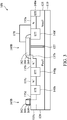
FIG. 3 shows a semiconductor device structure according to an embodiment of the invention. -
FIG. 4 shows a semiconductor device structure according to an embodiment of the invention. -
FIG. 5 shows a semiconductor device structure according to an embodiment of the invention. -
FIG. 6 shows the linear/saturation current (Idlin/Idsat) degradation after the HCI stress as a function of the healing gate voltage according to an embodiment of the invention. -
FIG. 7 shows the substrate currents with and without healing gate voltage as a function of gate voltage according to an embodiment of the invention. -
FIG. 8 shows a metal oxide semiconductor (MOS) transistor structure according to an embodiment of the invention. - The following description is of the best-contemplated mode of carrying out the invention. This description is made for the purpose of illustrating the general principles of the invention and should not be taken in a limiting sense. The scope of the invention is best determined by reference to the appended claims.
- Some variations of the embodiments are described. Throughout the various views and illustrative embodiments, like reference numbers are used to designate like elements. It should be understood that additional operations can be provided before, during, and/or after a disclosed method, and some of the operations described can be replaced or eliminated for other embodiments of the method.
- Furthermore, spatially relative terms, such as "beneath," "below," "lower," "above," "upper" and the like, may be used herein for ease of description to describe one element or feature's relationship to another element(s) or feature(s) as illustrated in the figures.
-
FIG. 1 shows asemiconductor device structure 10A according to an embodiment of the invention. A P-type well region 120 and an N-type well region 125 are formed over asemiconductor substrate 110. In some embodiments, thesemiconductor substrate 110 is a Si substrate. In some embodiments, the material of thesemiconductor substrate 110 is selected from a group consisting of bulk-Si, SiP, SiGe, SiC, SiPC, Ge, SOI-Si, SOI-SiGe, III-VI material, and a combination thereof. In some embodiments, a deep N-type well (not shown) is formed over thesemiconductor substrate 110, and the P-type well region 120 and the N-type well region 125 are formed over the deep N-type well. Awell region 127 is formed over thesemiconductor substrate 110 and between the P-type well region 120 and the N-type well region 125. In some embodiments, thewell region 127 is no dopant, i.e. thewell region 127 is not a P-type well region or an N-type well region. In some embodiments, thesemiconductor device structure 10A includes a laterally diffused metal oxide semiconductor (LDMOS) transistor. - The shallow trench isolation (STI)
regions type well region 120. A P-type doping region 130a is formed in the P-type well region 120 and between theSTI regions STI regions type well region 125. The P-type doping region 130c is formed in the N-type well region 125 and between theSTI regions type doping region 130b is formed in the N-type well region 125 and adjacent to theSTI region 140c. Furthermore, the P-type doping region 130b further includes a lightly dopedregion 132b. It should be noted that the size of the P-type doping region 130a is greater than that of the P-type doping regions - A
gate structure 160A is formed in thesemiconductor device structure 10A. Thegate structure 160A includes agate electrode 162, agate dielectric 164 under thegate electrode 162, and thespacers 166 formed on opposite sides of thegate electrode 162. Thespacers 166 may be formed by a single layer or multiple layers. In some embodiments, one or more work-function layers (not shown) are formed between thegate dielectric 164 and thegate electrode 162. Thegate dielectric 164 is disposed on thewell region 127 and partially over the P-type well region 120 and the N-type well region 125. Thespace 166 formed on the left side of thegate electrode 162 is disposed over the lightly dopedregion 132b, and thespace 166 formed on the right side of thegate electrode 162 is disposed over theSTI region 140b. A resist protective oxide (RPO) 170 is formed over a portion of thegate structure 160A, theSTI region 140b and a portion of the P-type doping region 130a. - The
gate dielectric 164 may include a silicon dioxide (referred to as silicon oxide) layer. Thegate dielectric 164 may be formed using chemical vapor deposition (CVD), physical vapor deposition (PVD), atomic layer deposition (ALD), thermal oxide, other suitable processes, or combinations thereof. Furthermore, the core oxide is used for healing gate application, so as to gain better gate control ability. - The
gate electrode 162 is configured to be coupled to metal interconnects. Thegate electrode 162 may include a doped or non-doped polycrystalline silicon (or polysilicon). Alternatively, thegate electrode 162 may include a metal such as Al, Cu, W, Ti, Ta, TiN, TaN, NiSi, CoSi, other suitable conductive materials, or combinations thereof. Thegate electrode 162 may be formed by CVD, PVD, ALD, plating, and other proper processes. Thegate electrode 162 may have a multilayer structure and may be formed in a multiple-step process. - In the
semiconductor device structure 10A, a P-type transistor including thegate structure 160A is formed. In some embodiments, the P-type transistor is a P-type LDMOS transistor. The P-type doping region 130a forms the drain region of the P-type transistor, and the P-type doping region 130b forms the source region of the P-type transistor. Thegate structure 160A is separated from the drain region of the P-type transistor by theSTI region 140b. The channel region of the P-type transistor is formed between the P-type doping region 130b and thewell region 127 and under thegate dielectric 164. Furthermore, the P-type doping region 130c forms the bulk region of the P-type transistor. In some embodiments, the bulk region of the P-type transistor is formed by an N-type doping region. - The P-type transistor further includes a
gate structure 165A. Thegate structure 165A is an additional healing gate for the PMOS transistor, and thegate structure 165A includes agate electrode 162, agate dielectric 164 under thegate electrode 162, and thespacers 166 formed on opposite sides of thegate electrode 162. Thespacers 166 may be formed by a single layer or multiple layers. In some embodiments, one or more work-function layers (not shown) are formed between thegate dielectric 164 and thegate electrode 162. Thegate dielectric 164 is disposed on the N-type well region 125. As described above, thegate electrode 162 is configured to be coupled to interconnects. Thespace 166 formed on the left side of thegate electrode 162 is disposed over the P-type doping region 130e, and thespace 166 formed on the right side of thegate electrode 162 is disposed over the P-type doping region 130d. Furthermore, no interconnect is coupled to the P-type doping regions gate structure 165A. In some embodiments, only thegate structure 165A is formed in thesemiconductor device structure 10A without the P-type doping regions gate structure 160A is greater than the gate length L2 of thegate structure 165A. -
FIG. 2 shows a healing mechanism in thesemiconductor device structure 10A ofFIG. 1 according to an embodiment of the invention. During hot-carrier instability (HCI) stress, vertical and horizontalelectrical fields 210 will accelerate hot hole/electron to break Si-H bonds. The dangling bonds become charged to cause mobility degradation, threshold voltage shift, and channel current degradation. By using the healing gate (i.e. thegate structure 165A), thehealing field 220 which reverse to thestress field 210 during the HCI stress suppresses impact ionization and also de-traps the HCI-induced trapped charge in thegate dielectric 164. By applying thehealing field 220, stability against HCI is improved for higher voltage application without enlarging channel length. -
FIG. 3 shows asemiconductor device structure 10B according to an embodiment of the invention. The P-type well region 120 and the N-type well region 125 are formed over asemiconductor substrate 110. In some embodiments, a deep N-type well (not shown) is formed over thesemiconductor substrate 110, and the P-type well region 120 and the N-type well region 125 are formed over the deep N-type well. Awell region 127 is formed over thesemiconductor substrate 110 and between the P-type well region 120 and the N-type well region 125. In some embodiments, thewell region 127 is no dopant, i.e. thewell region 127 is not a P-type well region or an N-type well region. In some embodiments, thesemiconductor device structure 10B includes a LDMOS transistor. - The
STI regions type well region 125. An N-type doping region 135a is formed in the N-type well region 125 and between theSTI regions STI regions type well region 120. The N-type doping region 135c is formed in the P-type well region 120 and between theSTI regions type doping region 135b is formed in the P-type well region 120 and adjacent to theSTI region 140g. Furthermore, the N-type doping region 135b further includes a lightly dopedregion 137b. It should be noted that the size of the N-type doping region 135a is greater than that of the N-type doping regions - A
gate structure 160B is formed in thesemiconductor device structure 10B. Thegate structure 160B includes agate electrode 162, agate dielectric 164 under thegate electrode 162, and thespacers 166 formed on opposite sides of thegate electrode 162. Thespacers 166 may be formed by a single layer or multiple layers. In some embodiments, one or more work-function layers (not shown) are formed between thegate dielectric 164 and thegate electrode 162. Thegate dielectric 164 is disposed on thewell region 127 and partially over the P-type well region 120 and the N-type well region 125. Thespace 166 formed on the left side of thegate electrode 162 is disposed over the lightly dopedregion 137b, and thespace 166 formed on the right side of thegate electrode 162 is disposed over theSTI region 140f. A resist protective oxide (RPO) 170 is formed over a portion of thegate structure 160B, theSTI region 140f and a portion of the N-type doping region 135a. - In the
semiconductor device structure 10B, an N-type transistor including thegate structure 160B is formed. In some embodiments, the N-type transistor is an N-type LDMOS transistor. The N-type doping region 135a forms the drain region of the N-type transistor, and the N-type doping region 135b forms the source region of the N-type transistor. The channel region of the N-type transistor is formed between the N-type doping region 135b and thewell region 127 and under thegate dielectric 164. Furthermore, the N-type doping region 135c forms the bulk region of the N-type transistor. In some embodiments, the bulk region of the N-type transistor is formed by a P-type doping region. - The N-type transistor further includes a
gate structure 165B. Thegate structure 165B is an additional healing gate for the N-type transistor, and thegate structure 165B includes agate electrode 162, agate dielectric 164 under thegate electrode 162, and thespaces 166 formed on opposite sides of thegate electrode 162. Thespacers 166 may be formed by a single layer or multiple layers. In some embodiments, one or more work-function layers (not shown) are formed between thegate dielectric 164 and thegate electrode 162. Thegate dielectric 164 is disposed on the P-type well region 120. As described above, thegate electrode 162 is configured to be coupled to interconnects. Thespace 166 formed on the left side of thegate electrode 162 is disposed over the N-type doping region 135e, and thespace 166 formed on the right side of thegate electrode 162 is disposed over the N-type doping region 135d. Furthermore, no interconnect is coupled to the N-type doping regions gate structure 165B. In some embodiments, only thegate structure 165B is formed in thesemiconductor device structure 10B without the P-type doping regions - Referring to
FIG. 1 andFIG. 3 together, the configuration of thesemiconductor device structure 10A ofFIG. 1 is similar to the configuration of thesemiconductor device structure 10B ofFIG. 2 . The difference between thesemiconductor device structure 10A including the P-type transistor and thesemiconductor device structure 10B including the N-type transistor is that the well regions and the doping regions in thesemiconductor device structures -
FIG. 4 shows asemiconductor device structure 10C according to an embodiment of the invention. Thesemiconductor device structure 10C includes a P-type transistor with thegate structures semiconductor device structure 10C ofFIG. 4 is similar to the configuration of thesemiconductor device structure 10A ofFIG. 1 . The difference between thesemiconductor device structure 10C and thesemiconductor device structure 10A is that nowell region 127 is formed between the P-type well region 120 and the N-type well region 125 in thesemiconductor device structure 10C. In other words, the P-type well region 120 is in direct contact with the N-type well region 125 in thesemiconductor device structure 10C. Similarly, by changing the type of conductivity of the well regions and the doping regions in thesemiconductor device structure 10C, an N-type transistor is obtained in thesemiconductor device structure 10C. In some embodiments, the N-type transistor is an N-type LDMOS transistor. -
FIG. 5 shows asemiconductor device structure 10D according to an embodiment of the invention. Thesemiconductor device structure 10D includes a P-type transistor with thegate structures semiconductor device structure 10D ofFIG. 5 is similar to the configuration of thesemiconductor device structure 10C ofFIG. 4 . The difference between thesemiconductor device structure 10D and the semiconductordevice transistor structure 10C is that noSTI region 140b is formed in thesemiconductor device structure 10D, and the P-type doping region 130a extends to the space of thegate structure 160D to formed a P-type doping region 130f in the P-type well region 120 of thesemiconductor device structure 10D. The P-type doping region 130f is adjacent to theSTI region 140a and under a portion of theRPO 170. Furthermore, the P-type doping region 130f further includes a lightly dopedregion 132f, and the lightly dopedregion 132f is formed under the right side of thegate electrode 162 of thegate structure 160D. Similarly, by changing the type of conductivity of the well regions and the doping regions in thesemiconductor device structure 10D, an N-type transistor is obtained in thesemiconductor device structure 10D. In some embodiments, the N-type transistor is an N-type LDMOS transistor. - The semiconductor device structures with the healing gate in the embodiments have better ability to protect against HCI degradation in high-voltage applications.
FIG. 6 shows the linear/saturation current (Idlin/Idsat) degradation after the HCI stress as a function of the healing gate voltage according to an embodiment of the invention. InFIG. 6 , Idsat and Idlin current degradation is efficiently suppressed once a healing bias is applied during the HCI stress. The healing effect is stronger with increasing healing gate voltage and around 35% of HCI degradation can be healed with a healing gate voltage of 3.0V. However, a healing voltage higher than a specific value (e.g., 3V) is avoid to prevent breakdown problems at the healing gate structure. - The substrate current is also monitored with and without healing gate application during the HCI stress. HCI degradation is typically attributed to hot hole/electron injection which induce Si-H bond breaking. Once created, the dangling bond will become charged and consequently induce threshold voltage shift, channel current degradation, and substrate current increase.
FIG. 7 shows the substrate currents with and without healing gate voltage as a function of gate voltage according to an embodiment of the invention. Under the same stress condition, the substrate current is decreased once the healing gate structure is applied. The substrate current is typically attributed to high-energy carriers in the channel causing impact ionization and therefore often correlated with HCI. With increasing healing voltage, Si-H bond breaking is suppressed as well. -
FIG. 8 shows a metal oxide semiconductor (MOS)transistor structure 20 according to an embodiment of the invention. The N-type well region 125 is formed over thesemiconductor substrate 110. In some embodiments, a deep N-type well (not shown) is formed over thesemiconductor substrate 110, and the N-type well region 125 is formed over the deep N-type well. - The STI regions 140_1, 140_2 and 140_3 are formed in the N-
type well region 125. The P-type doping regions 130_1 and 130_2 are formed in the N-type well region 125. The P-type doping region 130_1 is formed in the N-type well region 125 and adjacent to the STI region 140_1, and the P-type doping region 130_1 further includes a lightly doped region 132_1. The P-type doping region 130_2 is formed in the N-type well region 125 and adjacent to theSTI region 140 2, and the P-type doping region 130_2 further includes a lightly doped region 132_2. It should be noted that the size of the P-type doping region 130_1 is equal to that of the P-type doping region 130 2. - A gate structure 160_1 is formed in the
MOS transistor structure 20. The gate structure 160_1 includes agate electrode 162, agate dielectric 164 under thegate electrode 162, and thespaces 166 formed on opposite sides of thegate electrode 162. Thespacers 166 may be formed by a single layer or multiple layers. In some embodiments, one or more work-function layers (not shown) are formed between thegate dielectric 164 and thegate electrode 162. Thegate dielectric 164 is disposed on the N-type well region 125. Thespace 166 formed on the left side of thegate electrode 162 is disposed over the lightly doped region 132_2, and thespace 166 formed on the right side of thegate electrode 162 is disposed over the lightly doped region 132_1. As described above, thegate electrode 162 is configured to be coupled to interconnects. - In the
MOS transistor structure 20, a P-type MOS transistor including the gate structure 160_1 is formed. The P-type doping region 130_1 forms the drain region of the P-type MOS transistor, and the P-type doping region 130_2 forms the source region of the P-type MOS transistor. The channel region of the P-type MOS transistor is formed between the P-type doping region 130_1 and the P-type doping region 130_2 and under thegate dielectric 164. Furthermore, an N-type doping region 135_1 forms the bulk region of the P-type MOS transistor. - The P-type MOS transistor further includes a gate structure 165_1. The gate structure 165_1 is an additional healing gate for the P-type MOS transistor, and the gate structure 165_1 includes a
gate electrode 162, agate dielectric 164 under thegate electrode 162, and thespaces 166 formed on opposite sides of thegate electrode 162. Thespacers 166 may be formed by a single layer or multiple layers. In some embodiments, one or more work-function layers (not shown) are formed between thegate dielectric 164 and thegate electrode 162. Thegate dielectric 164 is disposed on the N-type well region 125. As described above, thegate electrode 162 is configured to be coupled to interconnects. Thespace 166 formed on the left side of thegate electrode 162 is disposed over the P-type doping region 130_4, and thespace 166 formed on the right side of thegate electrode 162 is disposed over the P-type doping region 130_3. Furthermore, no interconnect is coupled to the P-type doping regions 130_3 and 130_4. It should be noted that no channel region is formed under the gate structure 165_1. In some embodiments, only the gate structure 165_1 is formed in theMOS transistor structure 20 without the P-type doping regions 130_3 and 130_4. In some embodiments, the gate length L3 of the gate structure 160_1 is greater than the gate length L4 of the gate structure 165_1. In some embodiments, the gate length L3 of the gate structure 160_1 is equal to the gate length L4 of the gate structure 165_1. Similarly, by changing the type of conductivity of the well regions and the doping regions in theMOS transistor structure 20, an N-type MOS transistor is obtained in theMOS transistor structure 20. - According to the embodiments, the self-healing MOSFETs are provided. By adding the healing gate structure, hot-carrier instability (HCI) degradation can be efficiently suppressed without the drawback of increasing leakage. Substrate current and time dependence of the HCI degradation (N-factor) are improved in the healing mechanism. With healing gate bias, the HCI stress injected hot carriers can be recovered and consequently the current degradation suppressed. In some embodiments, 30% reduction of HCI degradation can be achieved.
- According to one aspect of this disclosure, a semiconductor device structure is provided, comprising: a semiconductor substrate; a first well region over the semiconductor substrate and having a first type of conductivity; a second well region over the semiconductor substrate and having a second type of conductivity that is different from the first type of conductivity; a well region over the semiconductor substrate and between the first and second well regions, wherein the well region has a third type of conductivity that is different from the first type of conductivity and the second type of conductivity; a first gate structure of a transistor disposed on the well region and partially over the first and second well regions; a drain region of the transistor in the first well region and having the first type of conductivity; a source region of the transistor in the second well region and having the first type of conductivity; a bulk region of the transistor in the second well region and having the first type of conductivity; and a second gate structure of the transistor disposed on the second well region, wherein the second gate structure is separated from the first gate structure by the source region and the bulk region.
- In one of more variants of this aspect, the semiconductor device is such that it a gate length of the first gate structure is greater than that of the second gate structure; it comprises: a first shallow trench isolation (STI) region in the second well region, wherein the second gate structure is separated from the bulk region by the first STI region; and a second STI region in the second well region and between the source region and the bulk region; it comprises: a third STI region in the first well region, wherein the first gate structure is separated from the drain region by the third STI region; it comprises: a resist protect oxide (RPO) formed over a portion of the first gate structure and a portion of the drain region; the first type of conductivity is N-type, and the second type of conductivity is P-type, and the transistor is an N-type laterally diffused metal oxide semiconductor (LDMOS) transistor; and/or the first type of conductivity is P-type, and the second type of conductivity is N-type, and the transistor is a P-type LDMOS transistor.
- According to one aspect of this disclosure, a semiconductor device structure is provided, comprising: a semiconductor substrate; a first well region over the semiconductor substrate and having a first type of conductivity; a second well region over the semiconductor substrate and having a second type of conductivity that is different from the first type of conductivity; a first gate structure disposed partially over the first and second well regions; a drain region of the first type of conductivity in the first well region; a source region of the first type of conductivity in the second well region; a bulk region in the second well region; and a second gate structure disposed on the second well region, wherein the second gate structure is separated from the first gate structure by the source region and the bulk region, wherein gate length of the first gate structure is greater than that of the second gate structure.
- In one of more variants of this aspect, the semiconductor device is such that it comprises: a first shallow trench isolation (STI) region in the second well region, wherein the second gate structure is separated from the bulk region by the first STI region; and a second STI region in the second well region and between the source region and the bulk region; it comprises: a third STI region in the first well region, wherein the first gate structure is separated from the drain region by the third STI region; it comprises: a resist protect oxide (RPO) formed directly over a portion of the first gate structure, a portion of the drain region, and a portion of third STI region; it comprises: a resist protect oxide (RPO) formed directly over a portion of the first gate structure, and a portion of the drain region; the bulk region has the first type of conductivity; and/or it comprises: a doping region in the second well region and having the first type of conductivity, wherein the second gate structure is separated from the bulk region by the doping region.
- According to one aspect of this disclosure, a semiconductor device structure is provided, comprising: a semiconductor substrate; a first well region over the semiconductor substrate and having a first type of conductivity; a second well region over the semiconductor substrate and having a second type of conductivity that is different from the first type of conductivity; a first gate structure disposed partially over the first and second well regions; a drain region of the first type of conductivity in the first well region; a source region of the first type of conductivity in the second well region; a lightly doped region of the first type of conductivity in the second well region and under the first gate structure; and a second gate structure disposed on the second well region, wherein the second gate structure is separated from the first gate structure by the source region, wherein the lightly doped region is in direct contact with the source region.
- In one of more variants of this aspect, the semiconductor device is such that the gate length of the first gate structure is greater than that of the second gate structure; it comprises: a bulk region of the first type of conductivity in the second well region; it comprises: a first shallow trench isolation (STI) region in the second well region, wherein the second gate structure is separated from the bulk region by the first STI region; and a second STI region in the second well region and between the source region and the bulk region; it comprises: a third STI region in the first well region, wherein the first gate structure is separated from the drain region by the third STI region; and /or it comprises: a well region over the semiconductor substrate and between the first and second well regions, wherein the well region has a third type of conductivity that is different from the first type of conductivity and the second type of conductivity.
- While the invention has been described by way of example and in terms of the preferred embodiments, it is to be understood that the invention is not limited to the disclosed embodiments. On the contrary, it is intended to cover various modifications and similar arrangements (as would be apparent to those skilled in the art). Therefore, the scope of the appended claims should be accorded the broadest interpretation so as to encompass all such modifications and similar arrangements.
Claims (13)
- A semiconductor device structure, comprising:a semiconductor substrate;a first well region over the semiconductor substrate and having a first type of conductivity;a second well region over the semiconductor substrate and having a second type of conductivity that is different from the first type of conductivity;a well region over the semiconductor substrate and between the first and second well regions, wherein the well region has a third type of conductivity that is different from the first type of conductivity and the second type of conductivity;a first gate structure of a transistor disposed on the well region and partially over the first and second well regions;a drain region of the transistor in the first well region and having the first type of conductivity;a source region of the transistor in the second well region and having the first type of conductivity;a bulk region of the transistor in the second well region and having the first type of conductivity; anda second gate structure of the transistor disposed on the second well region,wherein the second gate structure is separated from the first gate structure by the source region and the bulk region.
- The semiconductor device structure as claimed in claim 1, wherein a gate length of the first gate structure is greater than that of the second gate structure.
- The semiconductor device structure as claimed in claim 1 or 2, further comprising:a first shallow trench isolation (STI) region in the second well region, wherein the second gate structure is separated from the bulk region by the first STI region; anda second STI region in the second well region and between the source region and the bulk region.
- The semiconductor device structure as claimed in one of the preceding claims, further comprising:
a third STI region in the first well region, wherein the first gate structure is separated from the drain region by the third STI region. - The semiconductor device structure as claimed in one of the preceding claims, further comprising:
a resist protect oxide (RPO) formed over a portion of the first gate structure and a portion of the drain region. - The semiconductor device structure as claimed in one of claims 1 to 4, further comprising:
a resist protect oxide (RPO) formed directly over a portion of the first gate structure, a portion of the drain region, and a portion of third STI region. - The semiconductor device structure as claimed in in one of claims 1 to 4, further comprising:
a resist protect oxide (RPO) formed directly over a portion of the first gate structure, and a portion of the drain region. - The semiconductor device structure as claimed in one of the preceding claims, wherein the first type of conductivity is N-type, and the second type of conductivity is P-type, and the transistor is an N-type laterally diffused metal oxide semiconductor (LDMOS) transistor.
- The semiconductor device structure as claimed in one of the preceding claims, wherein the first type of conductivity is P-type, and the second type of conductivity is N-type, and the transistor is a P-type LDMOS transistor.
- The semiconductor device structure as claimed in one of the preceding claims, further comprising:a doping region in the second well region and having the first type of conductivity,wherein the second gate structure is separated from the bulk region by the doping region.
- A semiconductor device structure as claimed in one of claims 1 to 9, further comprising:a lightly doped region of the first type of conductivity in the second well region and under the first gate structure; andwherein the lightly doped region is in direct contact with the source region.
- A semiconductor device structure, comprising:a semiconductor substrate;a first well region over the semiconductor substrate and having a first type of conductivity;a second well region over the semiconductor substrate and having a second type of conductivity that is different from the first type of conductivity;a first gate structure disposed partially over the first and second well regions;a drain region of the first type of conductivity in the first well region;a source region of the first type of conductivity in the second well region;a bulk region in the second well region; anda second gate structure disposed on the second well region,wherein the second gate structure is separated from the first gate structure by the source region and the bulk region,wherein gate length of the first gate structure is greater than that of the second gate structure.
- A semiconductor device structure, comprising:a semiconductor substrate;a first well region over the semiconductor substrate and having a first type of conductivity;a second well region over the semiconductor substrate and having a second type of conductivity that is different from the first type of conductivity;a first gate structure disposed partially over the first and second well regions;a drain region of the first type of conductivity in the first well region;a source region of the first type of conductivity in the second well region;a lightly doped region of the first type of conductivity in the second well region and under the first gate structure; anda second gate structure disposed on the second well region,wherein the second gate structure is separated from the first gate structure by the source region,wherein the lightly doped region is in direct contact with the source region.
Applications Claiming Priority (2)
| Application Number | Priority Date | Filing Date | Title |
|---|---|---|---|
| US201962851686P | 2019-05-23 | 2019-05-23 | |
| US16/853,889 US11367788B2 (en) | 2019-05-23 | 2020-04-21 | Semiconductor device structure |
Publications (2)
| Publication Number | Publication Date |
|---|---|
| EP3742498A1 true EP3742498A1 (en) | 2020-11-25 |
| EP3742498B1 EP3742498B1 (en) | 2024-11-06 |
Family
ID=70470867
Family Applications (1)
| Application Number | Title | Priority Date | Filing Date |
|---|---|---|---|
| EP20171542.2A Active EP3742498B1 (en) | 2019-05-23 | 2020-04-27 | Semiconductor device structure |
Country Status (4)
| Country | Link |
|---|---|
| US (1) | US11367788B2 (en) |
| EP (1) | EP3742498B1 (en) |
| CN (1) | CN111987161B (en) |
| TW (1) | TWI742668B (en) |
Families Citing this family (1)
| Publication number | Priority date | Publication date | Assignee | Title |
|---|---|---|---|---|
| US20240274669A1 (en) * | 2023-02-09 | 2024-08-15 | Taiwan Semiconductor Manufacturing Company, Ltd. | Structure and Method for High-Voltage Device |
Citations (6)
| Publication number | Priority date | Publication date | Assignee | Title |
|---|---|---|---|---|
| EP1291924A1 (en) * | 2001-09-10 | 2003-03-12 | STMicroelectronics S.r.l. | MOS semiconductor device having a body region |
| US20110156142A1 (en) * | 2009-12-24 | 2011-06-30 | Taiwan Semiconductor Manufacturing Company, Ltd. | High voltage device with partial silicon germanium epi source/drain |
| US20120199878A1 (en) * | 2011-02-03 | 2012-08-09 | Mayank Shrivastava | Drain Extended Field Effect Transistors and Methods of Formation Thereof |
| US20130134511A1 (en) * | 2011-11-30 | 2013-05-30 | Freescale Semiconductor, Inc. | Semiconductor Device with Self-Biased Isolation |
| US20170077293A1 (en) * | 2015-09-11 | 2017-03-16 | Macronix International Co., Ltd. | Semiconductor device having gate structures and manufacturing method thereof |
| US9871132B1 (en) * | 2016-08-15 | 2018-01-16 | Globalfoundries Singapore Pte. Ltd. | Extended drain metal-oxide-semiconductor transistor |
Family Cites Families (12)
| Publication number | Priority date | Publication date | Assignee | Title |
|---|---|---|---|---|
| US8354710B2 (en) | 2008-08-08 | 2013-01-15 | Infineon Technologies Ag | Field-effect device and manufacturing method thereof |
| US20100237439A1 (en) * | 2009-03-18 | 2010-09-23 | Ming-Cheng Lee | High-voltage metal-dielectric-semiconductor device and method of the same |
| TWI408810B (en) | 2010-11-29 | 2013-09-11 | Macronix Int Co Ltd | Low on-resistance reduces surface electric field lateral diffusion metal oxide semiconductor transistor |
| US9450056B2 (en) | 2012-01-17 | 2016-09-20 | Taiwan Semiconductor Manufacturing Company, Ltd. | Lateral DMOS device with dummy gate |
| US9159803B2 (en) * | 2012-08-21 | 2015-10-13 | Freescale Semiconductor, Inc. | Semiconductor device with HCI protection region |
| US10553687B2 (en) * | 2013-10-11 | 2020-02-04 | Taiwan Semiconductor Manufacturing Company, Ltd. | Semiconductor device having conductive feature overlapping an edge of an active region |
| KR102177431B1 (en) * | 2014-12-23 | 2020-11-11 | 주식회사 키 파운드리 | Semiconductor device |
| CN107437563B (en) * | 2016-05-27 | 2020-03-10 | 中芯国际集成电路制造(上海)有限公司 | LDMOS transistor and method of forming the same, and ESD device and method of forming the same |
| KR102495452B1 (en) | 2016-06-29 | 2023-02-02 | 삼성전자주식회사 | Semiconductor device |
| CN107564816B (en) * | 2016-06-30 | 2020-05-08 | 中芯国际集成电路制造(上海)有限公司 | LDMOS transistor and method of forming the same |
| GB2563380B (en) * | 2017-06-05 | 2020-09-09 | X-Fab Semiconductor Foundries Gmbh | A method of fabricating a laterally diffused metal oxide semiconductor transistor |
| US10050033B1 (en) * | 2017-09-13 | 2018-08-14 | Taiwan Semiconductor Manufacturing Co., Ltd. | High voltage integration for HKMG technology |
-
2020
- 2020-04-21 US US16/853,889 patent/US11367788B2/en active Active
- 2020-04-27 EP EP20171542.2A patent/EP3742498B1/en active Active
- 2020-05-14 CN CN202010407322.3A patent/CN111987161B/en active Active
- 2020-05-18 TW TW109116386A patent/TWI742668B/en active
Patent Citations (6)
| Publication number | Priority date | Publication date | Assignee | Title |
|---|---|---|---|---|
| EP1291924A1 (en) * | 2001-09-10 | 2003-03-12 | STMicroelectronics S.r.l. | MOS semiconductor device having a body region |
| US20110156142A1 (en) * | 2009-12-24 | 2011-06-30 | Taiwan Semiconductor Manufacturing Company, Ltd. | High voltage device with partial silicon germanium epi source/drain |
| US20120199878A1 (en) * | 2011-02-03 | 2012-08-09 | Mayank Shrivastava | Drain Extended Field Effect Transistors and Methods of Formation Thereof |
| US20130134511A1 (en) * | 2011-11-30 | 2013-05-30 | Freescale Semiconductor, Inc. | Semiconductor Device with Self-Biased Isolation |
| US20170077293A1 (en) * | 2015-09-11 | 2017-03-16 | Macronix International Co., Ltd. | Semiconductor device having gate structures and manufacturing method thereof |
| US9871132B1 (en) * | 2016-08-15 | 2018-01-16 | Globalfoundries Singapore Pte. Ltd. | Extended drain metal-oxide-semiconductor transistor |
Non-Patent Citations (2)
| Title |
|---|
| LIU S E ET AL: "High Voltage Tolerant Design with Advanced Process for TV Application", 2019 IEEE INTERNATIONAL RELIABILITY PHYSICS SYMPOSIUM (IRPS), IEEE, 31 March 2019 (2019-03-31), pages 1 - 4, XP033554680, DOI: 10.1109/IRPS.2019.8720421 * |
| WEN-YI CHEN ET AL: "Circuit and Layout Co-Design for ESD Protection in Bipolar-CMOS-DMOS (BCD) High-Voltage Process", IEEE TRANSACTIONS ON CIRCUITS AND SYSTEMS I: REGULAR PAPERS, IEEE, US, vol. 57, no. 5, 1 May 2010 (2010-05-01), pages 1039 - 1047, XP011333667, ISSN: 1549-8328, DOI: 10.1109/TCSI.2010.2043986 * |
Also Published As
| Publication number | Publication date |
|---|---|
| US11367788B2 (en) | 2022-06-21 |
| TWI742668B (en) | 2021-10-11 |
| EP3742498B1 (en) | 2024-11-06 |
| CN111987161A (en) | 2020-11-24 |
| TW202114212A (en) | 2021-04-01 |
| CN111987161B (en) | 2024-05-24 |
| US20200373428A1 (en) | 2020-11-26 |
Similar Documents
| Publication | Publication Date | Title |
|---|---|---|
| US8643090B2 (en) | Semiconductor devices and methods for manufacturing a semiconductor device | |
| US9748383B2 (en) | Transistor | |
| US8330219B2 (en) | Semiconductor device with high-voltage breakdown protection | |
| US9159803B2 (en) | Semiconductor device with HCI protection region | |
| US20050285218A1 (en) | Method of forming high voltage devices with retrograde well | |
| US8377787B2 (en) | Alternating-doping profile for source/drain of a FET | |
| JP4686829B2 (en) | Semiconductor device and manufacturing method of semiconductor device | |
| US7344947B2 (en) | Methods of performance improvement of HVMOS devices | |
| US8878294B2 (en) | Semiconductor device having a drain-gate isolation portion | |
| KR100734507B1 (en) | A structure for current leakage prevention of a high voltage device | |
| US7453127B2 (en) | Double-diffused-drain MOS device with floating non-insulator spacers | |
| US11367788B2 (en) | Semiconductor device structure | |
| US20170005093A1 (en) | Semiconductor Device with Split Work Functions | |
| US9825168B2 (en) | Semiconductor device capable of high-voltage operation | |
| US12543341B2 (en) | Transistor structure having a charge storage layer arranged between a field plate and a drift region | |
| US8643104B1 (en) | Lateral diffusion metal oxide semiconductor transistor structure | |
| KR100847827B1 (en) | Method of manufacturing a high voltage transistor | |
| CN1983633B (en) | High voltage semiconductor component and manufacturing method thereof | |
| KR100632057B1 (en) | How to Form a CMOS Transistor | |
| US9853142B2 (en) | Method of manufacturing a trench FET having a merged gate dielectric | |
| US20070126057A1 (en) | Lateral DMOS device insensitive to oxide corner loss | |
| US20250040178A1 (en) | Laterally-Diffused Metal-Oxide Semiconductor Devices with Reduced Gate Charge and Time-Dependent Dielectric Breakdown | |
| KR100961549B1 (en) | Semiconductor device with high voltage transistor and logic transistor | |
| JP2507981B2 (en) | Manufacturing method of complementary MIS transistor | |
| US20060124975A1 (en) | Dual work function gate in CMOS device |
Legal Events
| Date | Code | Title | Description |
|---|---|---|---|
| PUAI | Public reference made under article 153(3) epc to a published international application that has entered the european phase |
Free format text: ORIGINAL CODE: 0009012 |
|
| STAA | Information on the status of an ep patent application or granted ep patent |
Free format text: STATUS: THE APPLICATION HAS BEEN PUBLISHED |
|
| AK | Designated contracting states |
Kind code of ref document: A1 Designated state(s): AL AT BE BG CH CY CZ DE DK EE ES FI FR GB GR HR HU IE IS IT LI LT LU LV MC MK MT NL NO PL PT RO RS SE SI SK SM TR |
|
| AX | Request for extension of the european patent |
Extension state: BA ME |
|
| STAA | Information on the status of an ep patent application or granted ep patent |
Free format text: STATUS: REQUEST FOR EXAMINATION WAS MADE |
|
| 17P | Request for examination filed |
Effective date: 20210505 |
|
| RBV | Designated contracting states (corrected) |
Designated state(s): AL AT BE BG CH CY CZ DE DK EE ES FI FR GB GR HR HU IE IS IT LI LT LU LV MC MK MT NL NO PL PT RO RS SE SI SK SM TR |
|
| STAA | Information on the status of an ep patent application or granted ep patent |
Free format text: STATUS: EXAMINATION IS IN PROGRESS |
|
| 17Q | First examination report despatched |
Effective date: 20220126 |
|
| P01 | Opt-out of the competence of the unified patent court (upc) registered |
Effective date: 20230607 |
|
| GRAP | Despatch of communication of intention to grant a patent |
Free format text: ORIGINAL CODE: EPIDOSNIGR1 |
|
| STAA | Information on the status of an ep patent application or granted ep patent |
Free format text: STATUS: GRANT OF PATENT IS INTENDED |
|
| INTG | Intention to grant announced |
Effective date: 20240611 |
|
| RIN1 | Information on inventor provided before grant (corrected) |
Inventor name: ZENG, ZHENG Inventor name: KO, CHING-CHUNG Inventor name: LIAO, JING-CHYI |
|
| GRAS | Grant fee paid |
Free format text: ORIGINAL CODE: EPIDOSNIGR3 |
|
| GRAA | (expected) grant |
Free format text: ORIGINAL CODE: 0009210 |
|
| STAA | Information on the status of an ep patent application or granted ep patent |
Free format text: STATUS: THE PATENT HAS BEEN GRANTED |
|
| AK | Designated contracting states |
Kind code of ref document: B1 Designated state(s): AL AT BE BG CH CY CZ DE DK EE ES FI FR GB GR HR HU IE IS IT LI LT LU LV MC MK MT NL NO PL PT RO RS SE SI SK SM TR |
|
| REG | Reference to a national code |
Ref country code: GB Ref legal event code: FG4D |
|
| REG | Reference to a national code |
Ref country code: CH Ref legal event code: EP |
|
| REG | Reference to a national code |
Ref country code: DE Ref legal event code: R079 Ref document number: 602020040665 Country of ref document: DE Free format text: PREVIOUS MAIN CLASS: H01L0029780000 Ipc: H10D0030600000 |
|
| REG | Reference to a national code |
Ref country code: DE Ref legal event code: R096 Ref document number: 602020040665 Country of ref document: DE |
|
| REG | Reference to a national code |
Ref country code: IE Ref legal event code: FG4D |
|
| REG | Reference to a national code |
Ref country code: LT Ref legal event code: MG9D |
|
| REG | Reference to a national code |
Ref country code: NL Ref legal event code: MP Effective date: 20241106 |
|
| PG25 | Lapsed in a contracting state [announced via postgrant information from national office to epo] |
Ref country code: PT Free format text: LAPSE BECAUSE OF FAILURE TO SUBMIT A TRANSLATION OF THE DESCRIPTION OR TO PAY THE FEE WITHIN THE PRESCRIBED TIME-LIMIT Effective date: 20250306 Ref country code: IS Free format text: LAPSE BECAUSE OF FAILURE TO SUBMIT A TRANSLATION OF THE DESCRIPTION OR TO PAY THE FEE WITHIN THE PRESCRIBED TIME-LIMIT Effective date: 20250306 Ref country code: HR Free format text: LAPSE BECAUSE OF FAILURE TO SUBMIT A TRANSLATION OF THE DESCRIPTION OR TO PAY THE FEE WITHIN THE PRESCRIBED TIME-LIMIT Effective date: 20241106 |
|
| PG25 | Lapsed in a contracting state [announced via postgrant information from national office to epo] |
Ref country code: NL Free format text: LAPSE BECAUSE OF FAILURE TO SUBMIT A TRANSLATION OF THE DESCRIPTION OR TO PAY THE FEE WITHIN THE PRESCRIBED TIME-LIMIT Effective date: 20241106 Ref country code: FI Free format text: LAPSE BECAUSE OF FAILURE TO SUBMIT A TRANSLATION OF THE DESCRIPTION OR TO PAY THE FEE WITHIN THE PRESCRIBED TIME-LIMIT Effective date: 20241106 |
|
| REG | Reference to a national code |
Ref country code: AT Ref legal event code: MK05 Ref document number: 1740385 Country of ref document: AT Kind code of ref document: T Effective date: 20241106 |
|
| PG25 | Lapsed in a contracting state [announced via postgrant information from national office to epo] |
Ref country code: BG Free format text: LAPSE BECAUSE OF FAILURE TO SUBMIT A TRANSLATION OF THE DESCRIPTION OR TO PAY THE FEE WITHIN THE PRESCRIBED TIME-LIMIT Effective date: 20241106 |
|
| PG25 | Lapsed in a contracting state [announced via postgrant information from national office to epo] |
Ref country code: ES Free format text: LAPSE BECAUSE OF FAILURE TO SUBMIT A TRANSLATION OF THE DESCRIPTION OR TO PAY THE FEE WITHIN THE PRESCRIBED TIME-LIMIT Effective date: 20241106 |
|
| PG25 | Lapsed in a contracting state [announced via postgrant information from national office to epo] |
Ref country code: NO Free format text: LAPSE BECAUSE OF FAILURE TO SUBMIT A TRANSLATION OF THE DESCRIPTION OR TO PAY THE FEE WITHIN THE PRESCRIBED TIME-LIMIT Effective date: 20250206 |
|
| PG25 | Lapsed in a contracting state [announced via postgrant information from national office to epo] |
Ref country code: LV Free format text: LAPSE BECAUSE OF FAILURE TO SUBMIT A TRANSLATION OF THE DESCRIPTION OR TO PAY THE FEE WITHIN THE PRESCRIBED TIME-LIMIT Effective date: 20241106 Ref country code: GR Free format text: LAPSE BECAUSE OF FAILURE TO SUBMIT A TRANSLATION OF THE DESCRIPTION OR TO PAY THE FEE WITHIN THE PRESCRIBED TIME-LIMIT Effective date: 20250207 Ref country code: AT Free format text: LAPSE BECAUSE OF FAILURE TO SUBMIT A TRANSLATION OF THE DESCRIPTION OR TO PAY THE FEE WITHIN THE PRESCRIBED TIME-LIMIT Effective date: 20241106 |
|
| PG25 | Lapsed in a contracting state [announced via postgrant information from national office to epo] |
Ref country code: PL Free format text: LAPSE BECAUSE OF FAILURE TO SUBMIT A TRANSLATION OF THE DESCRIPTION OR TO PAY THE FEE WITHIN THE PRESCRIBED TIME-LIMIT Effective date: 20241106 |
|
| PG25 | Lapsed in a contracting state [announced via postgrant information from national office to epo] |
Ref country code: RS Free format text: LAPSE BECAUSE OF FAILURE TO SUBMIT A TRANSLATION OF THE DESCRIPTION OR TO PAY THE FEE WITHIN THE PRESCRIBED TIME-LIMIT Effective date: 20250206 |
|
| PG25 | Lapsed in a contracting state [announced via postgrant information from national office to epo] |
Ref country code: SM Free format text: LAPSE BECAUSE OF FAILURE TO SUBMIT A TRANSLATION OF THE DESCRIPTION OR TO PAY THE FEE WITHIN THE PRESCRIBED TIME-LIMIT Effective date: 20241106 |
|
| PGFP | Annual fee paid to national office [announced via postgrant information from national office to epo] |
Ref country code: DE Payment date: 20241121 Year of fee payment: 6 |
|
| PG25 | Lapsed in a contracting state [announced via postgrant information from national office to epo] |
Ref country code: DK Free format text: LAPSE BECAUSE OF FAILURE TO SUBMIT A TRANSLATION OF THE DESCRIPTION OR TO PAY THE FEE WITHIN THE PRESCRIBED TIME-LIMIT Effective date: 20241106 |
|
| PG25 | Lapsed in a contracting state [announced via postgrant information from national office to epo] |
Ref country code: EE Free format text: LAPSE BECAUSE OF FAILURE TO SUBMIT A TRANSLATION OF THE DESCRIPTION OR TO PAY THE FEE WITHIN THE PRESCRIBED TIME-LIMIT Effective date: 20241106 |
|
| PG25 | Lapsed in a contracting state [announced via postgrant information from national office to epo] |
Ref country code: RO Free format text: LAPSE BECAUSE OF FAILURE TO SUBMIT A TRANSLATION OF THE DESCRIPTION OR TO PAY THE FEE WITHIN THE PRESCRIBED TIME-LIMIT Effective date: 20241106 |
|
| PG25 | Lapsed in a contracting state [announced via postgrant information from national office to epo] |
Ref country code: SK Free format text: LAPSE BECAUSE OF FAILURE TO SUBMIT A TRANSLATION OF THE DESCRIPTION OR TO PAY THE FEE WITHIN THE PRESCRIBED TIME-LIMIT Effective date: 20241106 |
|
| PG25 | Lapsed in a contracting state [announced via postgrant information from national office to epo] |
Ref country code: CZ Free format text: LAPSE BECAUSE OF FAILURE TO SUBMIT A TRANSLATION OF THE DESCRIPTION OR TO PAY THE FEE WITHIN THE PRESCRIBED TIME-LIMIT Effective date: 20241106 |
|
| PG25 | Lapsed in a contracting state [announced via postgrant information from national office to epo] |
Ref country code: IT Free format text: LAPSE BECAUSE OF FAILURE TO SUBMIT A TRANSLATION OF THE DESCRIPTION OR TO PAY THE FEE WITHIN THE PRESCRIBED TIME-LIMIT Effective date: 20241106 |
|
| REG | Reference to a national code |
Ref country code: DE Ref legal event code: R097 Ref document number: 602020040665 Country of ref document: DE |
|
| PG25 | Lapsed in a contracting state [announced via postgrant information from national office to epo] |
Ref country code: SE Free format text: LAPSE BECAUSE OF FAILURE TO SUBMIT A TRANSLATION OF THE DESCRIPTION OR TO PAY THE FEE WITHIN THE PRESCRIBED TIME-LIMIT Effective date: 20241106 |
|
| PLBE | No opposition filed within time limit |
Free format text: ORIGINAL CODE: 0009261 |
|
| STAA | Information on the status of an ep patent application or granted ep patent |
Free format text: STATUS: NO OPPOSITION FILED WITHIN TIME LIMIT |
|
| 26N | No opposition filed |
Effective date: 20250807 |
|
| REG | Reference to a national code |
Ref country code: CH Ref legal event code: H13 Free format text: ST27 STATUS EVENT CODE: U-0-0-H10-H13 (AS PROVIDED BY THE NATIONAL OFFICE) Effective date: 20251125 |
|
| PG25 | Lapsed in a contracting state [announced via postgrant information from national office to epo] |
Ref country code: LU Free format text: LAPSE BECAUSE OF NON-PAYMENT OF DUE FEES Effective date: 20250427 |
|
| PG25 | Lapsed in a contracting state [announced via postgrant information from national office to epo] |
Ref country code: MC Free format text: LAPSE BECAUSE OF FAILURE TO SUBMIT A TRANSLATION OF THE DESCRIPTION OR TO PAY THE FEE WITHIN THE PRESCRIBED TIME-LIMIT Effective date: 20241106 |
|
| REG | Reference to a national code |
Ref country code: BE Ref legal event code: MM Effective date: 20250430 |
|
| PG25 | Lapsed in a contracting state [announced via postgrant information from national office to epo] |
Ref country code: BE Free format text: LAPSE BECAUSE OF NON-PAYMENT OF DUE FEES Effective date: 20250430 |
|
| PG25 | Lapsed in a contracting state [announced via postgrant information from national office to epo] |
Ref country code: CH Free format text: LAPSE BECAUSE OF NON-PAYMENT OF DUE FEES Effective date: 20250430 |
|
| PGFP | Annual fee paid to national office [announced via postgrant information from national office to epo] |
Ref country code: GB Payment date: 20260312 Year of fee payment: 7 |
|
| PG25 | Lapsed in a contracting state [announced via postgrant information from national office to epo] |
Ref country code: IE Free format text: LAPSE BECAUSE OF NON-PAYMENT OF DUE FEES Effective date: 20250427 |
|
| PGFP | Annual fee paid to national office [announced via postgrant information from national office to epo] |
Ref country code: FR Payment date: 20260309 Year of fee payment: 7 |