EP3742485B1 - Layered super-reticle computing: architectures and methods - Google Patents
Layered super-reticle computing: architectures and methods Download PDFInfo
- Publication number
- EP3742485B1 EP3742485B1 EP20166445.5A EP20166445A EP3742485B1 EP 3742485 B1 EP3742485 B1 EP 3742485B1 EP 20166445 A EP20166445 A EP 20166445A EP 3742485 B1 EP3742485 B1 EP 3742485B1
- Authority
- EP
- European Patent Office
- Prior art keywords
- tile
- layer
- computing
- physical
- memory
- Prior art date
- Legal status (The legal status is an assumption and is not a legal conclusion. Google has not performed a legal analysis and makes no representation as to the accuracy of the status listed.)
- Active
Links
Images





Classifications
-
- G—PHYSICS
- G06—COMPUTING OR CALCULATING; COUNTING
- G06F—ELECTRIC DIGITAL DATA PROCESSING
- G06F1/00—Details not covered by groups G06F3/00 - G06F13/00 and G06F21/00
- G06F1/16—Constructional details or arrangements
- G06F1/18—Packaging or power distribution
- G06F1/183—Internal mounting support structures, e.g. for supporting printed circuit boards
-
- G—PHYSICS
- G06—COMPUTING OR CALCULATING; COUNTING
- G06F—ELECTRIC DIGITAL DATA PROCESSING
- G06F15/00—Digital computers in general; Data processing equipment in general
- G06F15/76—Architectures of general purpose stored program computers
-
- G—PHYSICS
- G06—COMPUTING OR CALCULATING; COUNTING
- G06F—ELECTRIC DIGITAL DATA PROCESSING
- G06F9/00—Arrangements for program control, e.g. control units
- G06F9/06—Arrangements for program control, e.g. control units using stored programs, i.e. using an internal store of processing equipment to receive or retain programs
- G06F9/46—Multiprogramming arrangements
- G06F9/50—Allocation of resources, e.g. of the central processing unit [CPU]
- G06F9/5005—Allocation of resources, e.g. of the central processing unit [CPU] to service a request
- G06F9/5027—Allocation of resources, e.g. of the central processing unit [CPU] to service a request the resource being a machine, e.g. CPUs, Servers, Terminals
-
- H—ELECTRICITY
- H10—SEMICONDUCTOR DEVICES; ELECTRIC SOLID-STATE DEVICES NOT OTHERWISE PROVIDED FOR
- H10W—GENERIC PACKAGES, INTERCONNECTIONS, CONNECTORS OR OTHER CONSTRUCTIONAL DETAILS OF DEVICES COVERED BY CLASS H10
- H10W70/00—Package substrates; Interposers; Redistribution layers [RDL]
- H10W70/60—Insulating or insulated package substrates; Interposers; Redistribution layers
- H10W70/611—Insulating or insulated package substrates; Interposers; Redistribution layers for connecting multiple chips together
-
- H—ELECTRICITY
- H10—SEMICONDUCTOR DEVICES; ELECTRIC SOLID-STATE DEVICES NOT OTHERWISE PROVIDED FOR
- H10W—GENERIC PACKAGES, INTERCONNECTIONS, CONNECTORS OR OTHER CONSTRUCTIONAL DETAILS OF DEVICES COVERED BY CLASS H10
- H10W70/00—Package substrates; Interposers; Redistribution layers [RDL]
- H10W70/60—Insulating or insulated package substrates; Interposers; Redistribution layers
- H10W70/62—Insulating or insulated package substrates; Interposers; Redistribution layers characterised by their interconnections
- H10W70/63—Vias, e.g. via plugs
- H10W70/635—Through-vias
-
- H—ELECTRICITY
- H10—SEMICONDUCTOR DEVICES; ELECTRIC SOLID-STATE DEVICES NOT OTHERWISE PROVIDED FOR
- H10W—GENERIC PACKAGES, INTERCONNECTIONS, CONNECTORS OR OTHER CONSTRUCTIONAL DETAILS OF DEVICES COVERED BY CLASS H10
- H10W70/00—Package substrates; Interposers; Redistribution layers [RDL]
- H10W70/60—Insulating or insulated package substrates; Interposers; Redistribution layers
- H10W70/62—Insulating or insulated package substrates; Interposers; Redistribution layers characterised by their interconnections
- H10W70/65—Shapes or dispositions of interconnections
-
- H—ELECTRICITY
- H10—SEMICONDUCTOR DEVICES; ELECTRIC SOLID-STATE DEVICES NOT OTHERWISE PROVIDED FOR
- H10W—GENERIC PACKAGES, INTERCONNECTIONS, CONNECTORS OR OTHER CONSTRUCTIONAL DETAILS OF DEVICES COVERED BY CLASS H10
- H10W80/00—Direct bonding of chips, wafers or substrates
-
- H—ELECTRICITY
- H10—SEMICONDUCTOR DEVICES; ELECTRIC SOLID-STATE DEVICES NOT OTHERWISE PROVIDED FOR
- H10W—GENERIC PACKAGES, INTERCONNECTIONS, CONNECTORS OR OTHER CONSTRUCTIONAL DETAILS OF DEVICES COVERED BY CLASS H10
- H10W90/00—Package configurations
-
- H—ELECTRICITY
- H10—SEMICONDUCTOR DEVICES; ELECTRIC SOLID-STATE DEVICES NOT OTHERWISE PROVIDED FOR
- H10W—GENERIC PACKAGES, INTERCONNECTIONS, CONNECTORS OR OTHER CONSTRUCTIONAL DETAILS OF DEVICES COVERED BY CLASS H10
- H10W90/00—Package configurations
- H10W90/401—Package configurations characterised by multiple insulating or insulated package substrates, interposers or RDLs
-
- H—ELECTRICITY
- H10—SEMICONDUCTOR DEVICES; ELECTRIC SOLID-STATE DEVICES NOT OTHERWISE PROVIDED FOR
- H10W—GENERIC PACKAGES, INTERCONNECTIONS, CONNECTORS OR OTHER CONSTRUCTIONAL DETAILS OF DEVICES COVERED BY CLASS H10
- H10W72/00—Interconnections or connectors in packages
- H10W72/01—Manufacture or treatment
-
- H—ELECTRICITY
- H10—SEMICONDUCTOR DEVICES; ELECTRIC SOLID-STATE DEVICES NOT OTHERWISE PROVIDED FOR
- H10W—GENERIC PACKAGES, INTERCONNECTIONS, CONNECTORS OR OTHER CONSTRUCTIONAL DETAILS OF DEVICES COVERED BY CLASS H10
- H10W90/00—Package configurations
- H10W90/20—Configurations of stacked chips
- H10W90/297—Configurations of stacked chips characterised by the through-semiconductor vias [TSVs] in the stacked chips
Definitions
- a processor tile may include a computing element, a processor core, a core, a processing engine, an execution unit, a central processing unit (CPU), caches, switches, and other components.
- a large number of processor tiles may be formed on a die. Efforts to advance the performance of HPC system ICs may have focused largely on advancing performance of component parts while holding the division of labor for a workload between the components relatively stable. Incremental advances in component performance are ultimately bounded.
- Embodiments herein may address two primary limits on the performance of HPC systems: energy efficiency and throughput per unit area of the computing ICs.
- Embodiments herein present three dimensional dataflow computing ICs, which are an architecture including multiple physical layers, e.g., a physical network layer, a physical computing layer, and a physical memory layer. Other physical layers or device layers may be included as well, e.g., a power delivery layer, an input/output (I/O) layer, or a communication layer.
- the physical network layer may be above the physical memory layer, and the physical computing layer may be above the physical network layer, hence forming a three dimensional dataflow computing device.
- the multiple dies in a physical layer may form a super-reticle to expand the two dimensional surface area to fill the available surface area of the U-card.
- a super-reticle formed by multiple dies may be used for other physical layers, e.g., the computing layer.
- computing is performed essentially at per-board level, e.g., compute-per-lU-server.
- the integration of thousands of low power cores, integrated memory, and a mesh network effectively compresses many racks of standard server hardware down to a single server tray.
- a customer immediately saves floor space and power while achieving high and repeatable performance. For example, a customer may achieve an improvement of 6x in throughput per 1U server and 15x in performance-per-Watt over a baseline performance modeled on the evolving A21/A23 supercomputers. Additionally, multiples of these three-dimensional dataflow computing ICs with multiple physical layers can create supercomputer-grade systems with far less assembly and management hassle. In addition, the dataflow computation based design enables basic advances in run-time repeatability, precision performance modeling, and sensitivity to manufacturing yield. Embodiments herein may be used to perform some computation intensive operations such as matrix multiplications. They can be used as an accelerator to work with a host, or independently for various applications, such as the current applications for enterprise data center computing for data-driven, customer-facing online services, including financial services, healthcare, travel, and more.
- Embodiments herein may present an integrated circuit including a physical network layer, a physical computing layer, and a physical memory layer.
- the physical network layer includes a first set of dies, and has a first side and a second side opposite to the first side.
- a die of the first set of dies includes multiple tiles.
- the physical network layer further includes one or more signal pathways dynamically configurable between multiple predefined interconnect topologies for the multiple tiles, where each topology of the multiple pre-defined interconnect topologies corresponds to a communication pattern related to a workload.
- the physical computing layer has a second set of dies. At least a die of the second set of dies includes multiple tiles, and is adjacent to the first side of the physical network layer.
- the physical memory layer has a third set of dies.
- Embodiments herein may present a computing system including a printed circuit board (PCB), a host attached to the PCB, and a semiconductor package including an integrated circuit.
- the integrated circuit includes a physical network layer, a physical computing layer, and a physical memory layer.
- the host and the semiconductor package including the integrated circuit are placed on the PCB, while the physical memory layer of the integrated circuit is closer to a top surface of the PCB than the physical computing layer of the integrated circuit.
- the physical network layer includes a first set of dies, and has a first side and a second side opposite to the first side.
- a die of the first set of dies includes multiple tiles.
- the physical network layer further includes one or more signal pathways dynamically configurable between multiple pre-defined interconnect topologies for the multiple tiles, where each topology of the multiple pre-defined interconnect topologies corresponds to a communication pattern related to a workload.
- the physical computing layer has a second set of dies. At least a die of the second set of dies includes multiple tiles, and is adjacent to the first side of the physical network layer.
- the physical memory layer has a third set of dies. At least a die of the third set of dies includes multiple tiles, and is adjacent to the second side of the physical network layer.
- a tile of the memory layer includes one or more storage cells. At least a tile in the physical computing layer is further arranged to move data to another tile in the physical computing layer or a storage cell of the physical memory layer through the one or more signal pathways in the physical network layer.
- Embodiments herein may present an integrated circuit including one or more tile stacks.
- a tile stack of the one or more tile stacks includes a computing tile in a physical computing layer, a network tile in a physical network layer, a tile of a control sublayer of a physical memory layer, and one or more storage tiles of one or more storage sublayers of the physical memory layer.
- the computing tile, the network tile, the tile of a control sublayer, and the one or more storage tiles are substantially vertically aligned.
- the computing tile includes an input/output (I/O) interface, a memory interface, a scratch memory, interconnects, and at least a computing element selected from a processor core, a configurable spatial array (CSA), an application specific integrated circuit (ASIC), a central processing unit (CPU), a processing engine (PE), a dataflow fabric.
- the network tile includes a virtual circuit (VC) portal to form a segment of a virtual circuit for a single-hop circuit-switched network to support circuit-switching.
- the one or more storage tiles include multiple storage cells.
- module or “routine” may refer to, be part of, or include an Application Specific Integrated Circuit (ASIC), an electronic circuit, a processor (shared, dedicated, or group) and/or memory (shared, dedicated, or group) that execute one or more software or firmware programs, a combinational logic circuit, and/or other suitable components that provide the described functionality.
- ASIC Application Specific Integrated Circuit
- processor shared, dedicated, or group
- memory shared, dedicated, or group
- Coupled may mean one or more of the following. “Coupled” may mean that two or more elements are in direct physical or electrical contact. However, “coupled” may also mean that two or more elements indirectly contact each other, but yet still cooperate or interact with each other, and may mean that one or more other elements are coupled or connected between the elements that are said to be coupled with each other. By way of example and not limitation, “coupled” may mean two or more elements or devices are coupled by electrical connections on a printed circuit board such as a motherboard, for example.
- Coupled may mean two or more elements/devices cooperate and/or interact through one or more network linkages such as wired and/or wireless networks.
- a computing apparatus may include two or more computing devices “coupled” on a motherboard or by one or more network linkages.
- circuitry may refer to, be part of, or include an Application Specific Integrated Circuit (ASIC), an electronic circuit, a processor (shared, dedicated, or group), and/or memory (shared, dedicated, or group) that execute one or more software or firmware programs, a combinational logic circuit, and/or other suitable hardware components that provide the described functionality.
- ASIC Application Specific Integrated Circuit
- computer-implemented method may refer to any method executed by one or more processors, a computer system having one or more processors, a mobile device such as a smartphone (which may include one or more processors), a tablet, a laptop computer, a set-top box, a gaming console, and so forth.
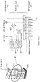
- Figures 1(a)-1(c) illustrate an exemplary computing system 100 including a computing IC 110, a computing IC 120, or a computing IC 140, formed with multiple physical layers that include multiple dies and tiles, in accordance with various embodiments.
- the computing system 100 includes the computing IC 110, which is included in a semiconductor package 103.
- the semiconductor package 103 is placed on a board, e.g., a printed circuit board (PCB), 101.
- the board 101 may include a host or a controller 102, so that the controller 102 and the computing IC 110 may work together to accomplishing desired functions.
- the controller 102 may perform control related operations while the computing device 110 may perform more computation intensive operations, e.g., matrix multiplication.
- the computing IC 110 may be used as a hardware accelerator to the controller 102.
- a computing IC e.g., the computing IC 110, 120, or 140, may be simply referred to as a computing device.
- the computing device 110 may include multiple physical layers, e.g., a physical network layer 107, a physical computing layer 105, and a physical memory layer 109 (hereinafter, simply a network layer 107, a computing layer 105, and a memory layer 109).
- a physical network layer 107 e.g., a physical network layer 107, a physical computing layer 105, and a physical memory layer 109
- other physical layers may be included as well, e.g., a physical power delivery layer, or a physical communication layer, not shown.
- the network layer 107 has a first side and a second side opposite to the first side.
- the computing layer 105 is adjacent to the first side of the network layer 107 and the memory layer 109 is adjacent to the second side of the network layer 107.
- one or more of the network layer 107, the computing layer 105, or the memory layer 109 each includes multiple dies, e.g., a die 112.
- the network layer 107 may include a first set of dies
- the computing layer 105 may include a second set of dies
- the memory layer 109 may include a third set of dies. At least a die of the second set of dies is adjacent to the first side of the network layer 107, and at least a die of the third set of dies is adjacent to the second side of the network layer 107.
- a die of the multiple dies includes multiple tiles, e.g., a tile 114.
- a die of the first set of dies for the network layer 107 includes multiple tiles
- at least a die of the second set of dies for the computing layer 105 includes multiple tiles
- at least a die of the third set of dies for the memory layer 109 includes multiple tiles.
- a tile of the memory layer 109 includes one or more storage cells. In some embodiments, there may be up to about O(10 4 ) tiles on the network layer 107, the computing layer 105, or the memory layer 109.
- the network layer 107 may include a single-hop circuit-switched network to support circuit-switching, where the single-hop circuit-switched network is configured by software.
- the single-hop circuit-switched network may include one or more signal pathways or virtual circuits (VC).
- VC virtual circuits
- the network layer 107 may include a VC 142 starting at a tile 141 and ending at a tile 143, where the VC 142 is a direct, unbuffered signal pathway extending through multiple tiles of the network layer 107.
- the network layer 107 may include one or more signal pathways or VCs, e.g., the VC 142, dynamically configurable between multiple pre-defined topologies for the multiple tiles on the die of the network layer 107.
- the network layer 107 may also include a multi-hop packet switched network to support packet-switching.
- data may move between two tiles in the computing layer 105 or between a tile in the computing layer 105 and a storage cell of the memory layer 109 through a signal pathway of the single-hop circuit-switched network in the network layer 107, or through a path in the multi-hop packet switched network in the network layer 107.
- a tile in the computing layer 105 is arranged to move data to another tile in the computing layer 105 or a storage cell of the memory layer 109 through the one or more signal pathways in the network layer 107.
- the computing IC 120 includes a network layer 127, a computing layer 125, and a memory layer 129, which may be similar to the network layer 107, the computing layer 105, and the memory layer 109.
- the memory layer 129 includes a control logic sublayer 131, and one or more storage cell sublayers 133 having storage cells.
- the network layer 127 or the computing layer 125 may also include one or more sublayers, not shown.
- a sublayer may refer to a single physical layer in a three dimensional grouping of layers.
- the computing IC 140 includes a network layer 147, a computing layer 145, and a memory layer 149, which may be similar to the network layer 107, the computing layer 105, and the memory layer 109.
- the IC 140 further includes an input/output (I/O) layer 148.
- the I/O layer 148 may be placed below memory layer 149. In some other embodiments, the I/O layer 148 may be placed in other locations. There may be further other layers, e.g., a power supply layer, a communication layer, not shown.
- the memory layer 149 includes a control logic sublayer 151, and one or more storage cell sublayers 153 having storage cells.
- the network layer 147, the computing layer 145, or the I/O layer 148 may also include one or more sublayers, not shown.
- dataflow execution model may be applied to the computing device 110.
- the regular design of tiles for the various physical layers may provide a systolic compute fabric leading to inherently stationary latency and throughput.
- the inherently stationary latency and throughput for the computing device 110 may be scale invariant with some small runtime variance.
- the multiple physical layers of the computing device 110 enable shorter distance and low energy interconnect between computing elements and large-capacity memory, compared to an alternative design of placing all the computing elements and large-capacity memory in a same layer.
- 80 fused multiply-add (FMA) computing components may access 64MB of memory positioned within 1.5mm, which may be difficult to achieve for other alternative designs.
- the low frequency design components used in the computing layer 105 can lower the thermal density, enabling three dimensional stacking. Extra-reticle patterning enables 2D scaling via simple repetition.
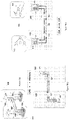
- the network layer 207, the computing layer 205, or the memory layer 209 may be bonded together by direct bonding, where one or more contact points 212 of a first tile in a first layer is in direct contact with one or more contact points of a second tile of a second layer, the first layer or the second layer may be selected from the network layer 207, the computing layer 205, or the memory layer 209.
- the computing IC 200 may include one or more tile stacks, e.g., a tile stack 210, which may be viewed as an atomic element of a complete computing system implemented as 3D stack of monolithic layers.
- the tile stack 210 includes a computing tile 215 in the computing layer 205, a network tile 217 in the network layer 207, and a tile 219 in the memory layer 209.
- the computing tile 215, the network tile 217, and the tile 219 in the memory layer 209 may be substantially vertically aligned, one over another.
- the computing tile 215, the network tile 217, and the tile 219 may represent multiple tiles stacked together.
- the tile 219 may include a tile of a control sublayer of the memory layer 209, and one or more storage tiles of one or more storage sublayers of the memory layer 209.
- any of the network layer 207, the computing layer 205, or the memory layer 209 may include multiple dies.
- the network layer 207 has a die 221, a die 223, a die 225, and other dies, which are on a super-reticle.
- Interconnect line 222 may be between the die 221 and the die 223 to couple a first device in the die 221 to a second device of the die 223, or between the die 221 and the die 225 to couple a first device in the die 221 to a second device of the die 225.
- the individual die may be of a size about 20 mm to about 30 mm, while the super-reticle formed for the network layer 207 may be of a size about 50 nm to about 75 mm, which may be 6 times larger than a single die.
- Other physical layers, e.g., the computing layer 205 and the memory layer 209 may be on a super-reticle as well. Additionally and alternatively, the computing layer 205 and the memory layer 209 may be designed differently as showing in Figures 3(a)-3(b) below.
- the computing IC 300 may include the network layer 307 formed on a super-reticle, which may be similar to the super-reticle for the network layer 207 shown in Figure 2 .
- the network layer 307 includes a super-reticle having multiple dies, e.g., a die 304, interconnected by interconnect lines.
- the computing layer 305 or the memory layer 309 may include one or more chiplets, e.g., a chiplet 302, or a chiplet 306.
- a chiplet may be a silicn die in a small form factor.
- a tile of a chiplet may be coupled or bonded to a tile of a die of the super-reticle for the network layer 307.
- the network layer 307 may include multiple tiles 311-318, organized into a radix 6 array shape with multiple rows, e.g., three rows.
- Each tile may have one or more contact points, which may be used for direct bonding or to contact with TSV. All the contact points of a tile are confined to an area less than or equal to 1 ⁇ 2 of the tile, e.g., a left half or a right left that is opposite to the left half of the tile. For example, at a first row, for the tile 316 and the tile 318, the contact points are at the right half of the tile area; at a second row, for the tile 311, the tile 313, and the tile 315, the contact points are at the left half of the tile area.
- the contact points are at the right half of the tile area.
- the pattern of the contact points can be continued for the network layer 307 so that if all the tiles in row n have their contact points on the left half, then all the tiles in row n + 1 have their contact points on the right half.
- the contact points of the tiles for the network layer 307 may result in an interface pattern as seen by other layers, e.g., the compute layer 305 or the memory layer 309 as a Cartesian array.
- the contact points 322 of the tile 312, the contact points 323 of the tile 313, and the contact points 326 of the tile 316 become vertically aligned.
- the contact points 322 of the tile 312 of the network layer 307 may be in direct contact with the contact points 344 of the tile 334 of the computing layer 305
- the contact points 323 of the tile 313 may be in direct contact with the contact points 345 of the tile 335
- the contact points 326 of the tile 316 may be in direct contact with the contact points 346 of the tile 336.
- the dataflow fabric 443 may be an architectural subset of the configurable spatial array dataflow fabric including about 256 PEs, operating with 200 MHz system clock.
- An operation performed by the dataflow fabric 443 may access data stored in the scratch memory 445 embedded in the dataflow fabric 443, or a memory bank in the memory tile 418.
- the bulk of the computing may take place on the dataflow fabric 443 with simplified memory access model.
- the computing tile 414 may have no support for coherency.
- the virtual-physical address translation may be embedded in the control logic of the memory tile 418.
- Input and output to the dataflow fabric 443 can come from the CPU 441, the memory interface 448, the network interface 444, or the VC ports 446.
- the scratch memory 445 within the dataflow fabric 443 may expand capacity and configurability of the dataflow fabric 443.
- VC portals that serve as terminal points or contact points for up to six point-to-point VCs.
- These VC portals can be configured by configuring a selector 442 to act as either a memory portal or a direct extension to the CSA dataflow fabric. In the latter mode, the CPU's on two cooperating tiles can created direct links between their dataflow fabric 443.
- the minimum access granularity for the 8 storage sublayers 453 may be single byte, and maximum transfer rate may be 8 bytes per cycle on each port.
- the memory tile 418 may also support unbuffered, single cycle reads.
- a memory stack configured as 16 banks @ 2MB per bank with a 200MHz system clock may deliver a bandwidth density of 26 GB/s per mm 2 .
- the 600 tiles covering the area of a standard reticle may deliver an aggregate of 15.3 TB/s of access bandwidth operating on 19.3 GB of storage.
- computing element 523 of computing tile 524 in tile stack 520 is configured to be coupled through VC 531 to computing element 513 of computing tile 514 in tile stack 510.
- VC 531 includes a first VC portal 521 of network tile 526 of tile stack 520 and a second VC portal 511 of network tile 516 of tile stack 510.
- Computing element 523 and computing element 513 may be a PE inside a dataflow fabric.
- VC 531 couples computing element 523 in the dataflow fabric in computing tile 524 to computing element 513 in the dataflow fabric in computing tile 514, extending the dataflow fabric from one computing tile to another tile.
- the computing system 100 may employ one or more tile stacks, e.g., tile stack 210, tile stack 410, tile stack 510, or tile stack 520, to perform operations, e.g., matrix-matrix multiplication.
- a performance model for matrix-matrix multiplication illustrates the power of the computing system 100 with the various tile stacks.
- the matrix multiplication operation may be instantiated as a single large dataflow graph and folded directly onto the tile stacks of the computing system 100. In an experiment, throughput is scaled by growing the size of the tile array and by expanding the dataflow graph to utilize the additional tiles. Performance is modeled as the tile array scales from 5K to 40K nodes, achieving 1 PFlop/s sustained performance at approximately 34K nodes.
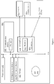
- the system 600 may include one or more processors 602, and one or more hardware accelerators 603.
- the hardware accelerator 603 may be an example of the computing IC 110, 120, 140, as shown in Figures 1(a)-1(c) , the computing IC 200 as shown in Figure 2 , the computing IC 300 as shown in Figures 3(a)-3(b) , with further details of a computing IC as shown in Figures 4(a)-4(d) , and in Figures 5(a)-5(c) .
- a software module 663 may be executed by the execution unit(s) 602.
- the computing system 600 may include a main memory device 604, which may be any one of a number of known persistent storage media, and a data storage circuitry 608.
- memory circuitry 604 can be any suitable type, number and/or combination of volatile memory devices (e.g., random access memory (RAM), dynamic RAM (DRAM), static RAM (SRAM), etc.) and/or non-volatile memory devices (e.g., read-only memory (ROM), erasable programmable read-only memory (EPROM), electrically erasable programmable read-only memory (EEPROM), flash memory, antifuses, etc.) that may be configured in any suitable implementation as are known.
- volatile memory devices e.g., random access memory (RAM), dynamic RAM (DRAM), static RAM (SRAM), etc.
- non-volatile memory devices e.g., read-only memory (ROM), erasable programmable read-only memory (EPROM), electrically erasable programmable read-only memory (EEPROM), flash memory, antifuses, etc.
- ROM read-only memory
- EPROM erasable programmable read-only memory
- EEPROM electrically erasable programmable read
- the number, capability and/or capacity of these elements 602-663 may vary, depending on the number of other devices the device 600 is configured to support. Otherwise, the constitutions of elements 602-661 are known, and accordingly will not be further described.
- a computer-usable or computer-readable medium could even be paper or another suitable medium upon which the program is printed, as the program can be electronically captured, via, for instance, optical scanning of the paper or other medium, then compiled, interpreted, or otherwise processed in a suitable manner, if necessary, and then stored in a computer memory.
- a computer-usable or computer-readable medium may be any medium that can contain, store, communicate, propagate, or transport the program for use by or in connection with the instruction execution system, apparatus, or device.
- the computer-usable medium may include a propagated data signal with the computer-usable program code embodied therewith, either in baseband or as part of a carrier wave.
- the computer usable program code may be transmitted using any appropriate medium, including but not limited to wireless, wireline, optical fiber cable, RF, etc.
Landscapes
- Engineering & Computer Science (AREA)
- Theoretical Computer Science (AREA)
- Physics & Mathematics (AREA)
- Computer Hardware Design (AREA)
- General Engineering & Computer Science (AREA)
- General Physics & Mathematics (AREA)
- Software Systems (AREA)
- Power Engineering (AREA)
- Human Computer Interaction (AREA)
- Semiconductor Memories (AREA)
- Geometry (AREA)
- Design And Manufacture Of Integrated Circuits (AREA)
Description
- Embodiments of the present disclosure relate generally to the technical field of computing, and more particularly to integrated circuits with multiple physical layers.
- The background description provided herein is for the purpose of generally presenting the context of the disclosure. Unless otherwise indicated herein, the materials described in this section are not prior art to the claims in this application and are not admitted to be prior art by inclusion in this section.
- Traditionally, high performance computing (HPC) and enterprise data center computing are optimized for different types of applications. Those within the data center are largely transaction-oriented while HPC applications crunch numbers and high volumes of data. However, driven by business-oriented analytics applications, e.g., Artificial intelligence (AI), HPC plays a more and more important role in data center computing. HPC systems have made tremendous progress, but still face many obstacles to further improve their performance. For example, the throughput per unit area and energy efficiency of integrated circuits (ICs) in current HPC systems may be limited. HPC systems may be built using multi-tile processor ICs that may include multiple processor tiles. A processor tile may include a computing element, a processor core, a core, a processing engine, an execution unit, a central processing unit (CPU), caches, switches, and other components. A large number of processor tiles may be formed on a die. Efforts to advance the performance of HPC system ICs may have focused largely on advancing performance of component parts while holding the division of labor for a workload between the components relatively stable. Incremental advances in component performance are ultimately bounded.
-
WO 2011/107612 discloses a method for creating electrical connections between a plurality of electronic circuit tiles on a same semiconductor die - it comprises selecting a plurality of electronic circuit tiles for being diced together, i.e. in one block, from a wafer so as to create a die comprising multiple electronic circuit tiles; and customizing one or more electrically conductive layers of the created die to make electrical connections between the selected plurality of electronic circuit tiles. - Embodiments will be readily understood by the following detailed description in conjunction with the accompanying drawings. To facilitate this description, like reference numerals designate like structural elements. Embodiments are illustrated by way of example and not by way of limitation in the figures of the accompanying drawings.
-
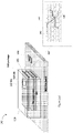
Figures 1(a)-1(c) illustrate an exemplary computing system including a computing integrated circuit (IC) formed with multiple physical layers that include multiple dies and tiles, in accordance with various embodiments. -
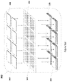
Figure 2 illustrates an exemplary computing IC including multiple physical layers formed by multiple dies and tiles, in accordance with various embodiments. -
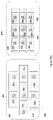
Figures 3(a)-3(b) illustrate another exemplary computing IC including multiple physical layers having multiple dies and tiles, in accordance with various embodiments. -
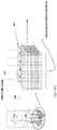
Figures 4(a)-4(d) illustrate more details of a multiple layer tile stack of an exemplary computing IC, in accordance with various embodiments. -
Figures 5(a)-5(c) illustrate more details of dataflow computations by multiple tile stacks of an exemplary computing IC, in accordance with various embodiments. -
Figure 6 illustrates an example computing system formed with computing ICs of the present disclosure, in accordance with various embodiments. -
Figure 7 illustrates a storage medium having instructions for implementing various system services and applications on a computing system formed with computing ICs described with references toFigures 1-6 , in accordance with various embodiments. - Enterprise data center computing are facing many new challenges for data-driven, customer-facing online services, including financial services, healthcare, and travel. The explosive, global growth of software as a service and online services is leading to major changes in enterprise infrastructure, with new application development methodologies, new database solutions, new infrastructure hardware and software technologies, and new datacenter management paradigms. As enterprise cloud infrastructures continue to grow in scale while delivering increasingly sophisticated analytics, High performance computing (HPC) systems may play a more and more important role in the data driven enterprise cloud computing.
- High performance computing (HPC) systems may be built using multi-tile processors, e.g. integrated circuits (ICs) with multiple processor tiles, or simply referred to as tiles. A processor tile may include a computing element, a processor core, a core, a processing engine, an execution unit, a central processing unit (CPU), caches, switches, and other components. A large number of processor tiles may be formed on a die. Each tile may be coupled to one or more neighboring tiles by interconnects according to a topology or an interconnect topology.
- Efforts to advance the performance of HPC systems have focused largely on advancing performance of component parts of HPC systems while holding the division of labor for a workload between the components relatively stable. For example, various technologies have been developed for higher performance sockets, higher bandwidth switching fabric, denser packaging, higher capacity cooling, faster and denser tile arrays, higher bandwidth on-die mesh, more efficient on-package routing, larger or faster memory stacks, or 3D logic stacking and near-memory compute. Incremental advances in component performance are ultimately bounded by the architectural fundamentals at the socket and board levels. For example, there may be a minimum energy cost to move a byte of data from a high bandwidth memory (HBM), e.g., DRAM stack, onto the tile array, through the memory hierarchy and on to the requesting core. Universal mesh-based interconnects may limit the aggregate injection rate of the tile array, and by extension, the number of tiles. For GHz clock rates, thermals may limit the number of transistors per mm2 that can switch simultaneously.
- Embodiments herein may address two primary limits on the performance of HPC systems: energy efficiency and throughput per unit area of the computing ICs. Embodiments herein present three dimensional dataflow computing ICs, which are an architecture including multiple physical layers, e.g., a physical network layer, a physical computing layer, and a physical memory layer. Other physical layers or device layers may be included as well, e.g., a power delivery layer, an input/output (I/O) layer, or a communication layer. The physical network layer may be above the physical memory layer, and the physical computing layer may be above the physical network layer, hence forming a three dimensional dataflow computing device. The terms, a physical network layer, a physical computing layer, or a physical memory layer refer to the fact that the physical network layer, the physical memory layer, and the physical computing layer are concrete objects in the real world, not an abstract layer just in a person's mind. For example, the physical network layer includes a first set of dies, the physical computing layer includes a second set of dies, and the physical memory layer incudes a third set of dies, which are all physical objects made from silicon or other technologies. On the other hand, circuits in dies on the physical network layer may perform similar functions, e.g., related to networking functions. Similarly, circuits in dies on the physical computing layer may perform mainly computing related functions, and circuits in dies on the physical memory layer may perform mainly memory related functions, e.g., storage cells. Therefore, each of the physical network layer, the physical memory layer, and the physical computing layer may also refer to a functional layer performing similar functions. In addition, in the description below, for simplicity reasons, a physical network layer, a physical memory layer, or a physical computing layer may be simply referred to as a network layer, a memory layer, or a computing layer.
- Embodiments herein may improve and overcome some technical obstacles that collectively bound performance of HPC systems, e.g., throughput per unit area and energy efficiency of the constituent computing ICs. The energy barrier may be overcome by shortening the distance from storage to a computing element, and from a computing element to another computing element, e.g., within a package. The performance barrier may be overcome with a packaging approach that includes the entire computing device with multiple physical layers within one package. Hence, the IC architecture may be viewed as an architecture for a super-reticle computer, where the super-reticle refers to the fact that multiple dies in a physical layer may be grouped together to form a super-reticle with an area size larger than a single die. The multiple dies in a physical layer, e.g., the network layer, may form a super-reticle to expand the two dimensional surface area to fill the available surface area of the U-card. In some embodiments, a super-reticle formed by multiple dies may be used for other physical layers, e.g., the computing layer. In some other embodiments, there may be only one physical layer, e.g., the network layer, includes a super-reticle. As a result, computing is performed essentially at per-board level, e.g., compute-per-lU-server. The integration of thousands of low power cores, integrated memory, and a mesh network effectively compresses many racks of standard server hardware down to a single server tray. A customer immediately saves floor space and power while achieving high and repeatable performance. For example, a customer may achieve an improvement of 6x in throughput per 1U server and 15x in performance-per-Watt over a baseline performance modeled on the evolving A21/A23 supercomputers. Additionally, multiples of these three-dimensional dataflow computing ICs with multiple physical layers can create supercomputer-grade systems with far less assembly and management hassle. In addition, the dataflow computation based design enables basic advances in run-time repeatability, precision performance modeling, and sensitivity to manufacturing yield. Embodiments herein may be used to perform some computation intensive operations such as matrix multiplications. They can be used as an accelerator to work with a host, or independently for various applications, such as the current applications for enterprise data center computing for data-driven, customer-facing online services, including financial services, healthcare, travel, and more.
- Embodiments herein may present an integrated circuit including a physical network layer, a physical computing layer, and a physical memory layer. The physical network layer includes a first set of dies, and has a first side and a second side opposite to the first side. A die of the first set of dies includes multiple tiles. The physical network layer further includes one or more signal pathways dynamically configurable between multiple predefined interconnect topologies for the multiple tiles, where each topology of the multiple pre-defined interconnect topologies corresponds to a communication pattern related to a workload. The physical computing layer has a second set of dies. At least a die of the second set of dies includes multiple tiles, and is adjacent to the first side of the physical network layer. The physical memory layer has a third set of dies. At least a die of the third set of dies includes multiple tiles, and is adjacent to the second side of the physical network layer. A tile of the memory layer includes one or more storage cells. At least one tile in the physical computing layer is further arranged to move data to another tile in the physical computing layer or a storage cell of the physical memory layer through the one or more signal pathways in the physical network layer.
- Embodiments herein may present a computing system including a printed circuit board (PCB), a host attached to the PCB, and a semiconductor package including an integrated circuit. The integrated circuit includes a physical network layer, a physical computing layer, and a physical memory layer. The host and the semiconductor package including the integrated circuit are placed on the PCB, while the physical memory layer of the integrated circuit is closer to a top surface of the PCB than the physical computing layer of the integrated circuit. The physical network layer includes a first set of dies, and has a first side and a second side opposite to the first side. A die of the first set of dies includes multiple tiles. The physical network layer further includes one or more signal pathways dynamically configurable between multiple pre-defined interconnect topologies for the multiple tiles, where each topology of the multiple pre-defined interconnect topologies corresponds to a communication pattern related to a workload. The physical computing layer has a second set of dies. At least a die of the second set of dies includes multiple tiles, and is adjacent to the first side of the physical network layer. The physical memory layer has a third set of dies. At least a die of the third set of dies includes multiple tiles, and is adjacent to the second side of the physical network layer. A tile of the memory layer includes one or more storage cells. At least a tile in the physical computing layer is further arranged to move data to another tile in the physical computing layer or a storage cell of the physical memory layer through the one or more signal pathways in the physical network layer.
- Embodiments herein may present an integrated circuit including one or more tile stacks. A tile stack of the one or more tile stacks includes a computing tile in a physical computing layer, a network tile in a physical network layer, a tile of a control sublayer of a physical memory layer, and one or more storage tiles of one or more storage sublayers of the physical memory layer. The computing tile, the network tile, the tile of a control sublayer, and the one or more storage tiles are substantially vertically aligned. The computing tile includes an input/output (I/O) interface, a memory interface, a scratch memory, interconnects, and at least a computing element selected from a processor core, a configurable spatial array (CSA), an application specific integrated circuit (ASIC), a central processing unit (CPU), a processing engine (PE), a dataflow fabric. The network tile includes a virtual circuit (VC) portal to form a segment of a virtual circuit for a single-hop circuit-switched network to support circuit-switching. The one or more storage tiles include multiple storage cells.
- In the description to follow, reference is made to the accompanying drawings that form a part hereof wherein like numerals designate like parts throughout, and in which is shown by way of illustration embodiments that may be practiced. It is to be understood that other embodiments may be utilized and structural or logical changes may be made without departing from the scope of the present disclosure. Therefore, the following detailed description is not to be taken in a limiting sense, and the scope of embodiments is defined by the appended claims and their equivalents.
- Operations of various methods may be described as multiple discrete actions or operations in turn, in a manner that is most helpful in understanding the claimed subject matter. However, the order of description should not be construed as to imply that these operations are necessarily order dependent. In particular, these operations may not be performed in the order of presentation. Operations described may be performed in a different order than the described embodiments. Various additional operations may be performed and/or described operations may be omitted, split or combined in additional embodiments.
- For the purposes of the present disclosure, the phrase "A or B" and "A and/or B" means (A), (B), or (A and B). For the purposes of the present disclosure, the phrase "A, B, and/or C" means (A), (B), (C), (A and B), (A and C), (B and C), or (A, B and C).
- The description may use the phrases "in an embodiment," or "in embodiments," which may each refer to one or more of the same or different embodiments. Furthermore, the terms "comprising," "including," "having," and the like, as used with respect to embodiments of the present disclosure, are synonymous.
- As used hereinafter, including the claims, the term "module" or "routine" may refer to, be part of, or include an Application Specific Integrated Circuit (ASIC), an electronic circuit, a processor (shared, dedicated, or group) and/or memory (shared, dedicated, or group) that execute one or more software or firmware programs, a combinational logic circuit, and/or other suitable components that provide the described functionality.
- Where the disclosure recites "a" or "a first" element or the equivalent thereof, such disclosure includes one or more such elements, neither requiring nor excluding two or more such elements. Further, ordinal indicators (e.g., first, second or third) for identified elements are used to distinguish between the elements, and do not indicate or imply a required or limited number of such elements, nor do they indicate a particular position or order of such elements unless otherwise specifically stated.
- The terms "coupled with" and "coupled to" and the like may be used herein. "Coupled" may mean one or more of the following. "Coupled" may mean that two or more elements are in direct physical or electrical contact. However, "coupled" may also mean that two or more elements indirectly contact each other, but yet still cooperate or interact with each other, and may mean that one or more other elements are coupled or connected between the elements that are said to be coupled with each other. By way of example and not limitation, "coupled" may mean two or more elements or devices are coupled by electrical connections on a printed circuit board such as a motherboard, for example. By way of example and not limitation, "coupled" may mean two or more elements/devices cooperate and/or interact through one or more network linkages such as wired and/or wireless networks. By way of example and not limitation, a computing apparatus may include two or more computing devices "coupled" on a motherboard or by one or more network linkages.
- As used herein, the term "circuitry" may refer to, be part of, or include an Application Specific Integrated Circuit (ASIC), an electronic circuit, a processor (shared, dedicated, or group), and/or memory (shared, dedicated, or group) that execute one or more software or firmware programs, a combinational logic circuit, and/or other suitable hardware components that provide the described functionality. As used herein, "computer-implemented method" may refer to any method executed by one or more processors, a computer system having one or more processors, a mobile device such as a smartphone (which may include one or more processors), a tablet, a laptop computer, a set-top box, a gaming console, and so forth.
-
Figures 1(a)-1(c) illustrate anexemplary computing system 100 including acomputing IC 110, acomputing IC 120, or acomputing IC 140, formed with multiple physical layers that include multiple dies and tiles, in accordance with various embodiments. - In embodiments, the
computing system 100 includes thecomputing IC 110, which is included in asemiconductor package 103. Thesemiconductor package 103 is placed on a board, e.g., a printed circuit board (PCB), 101. Theboard 101 may include a host or acontroller 102, so that thecontroller 102 and thecomputing IC 110 may work together to accomplishing desired functions. For example, thecontroller 102 may perform control related operations while thecomputing device 110 may perform more computation intensive operations, e.g., matrix multiplication. In some embodiments, thecomputing IC 110 may be used as a hardware accelerator to thecontroller 102. In the description below, a computing IC, e.g., thecomputing IC - In embodiments, the
computing device 110 may include multiple physical layers, e.g., aphysical network layer 107, aphysical computing layer 105, and a physical memory layer 109 (hereinafter, simply anetwork layer 107, acomputing layer 105, and a memory layer 109). In addition, other physical layers may be included as well, e.g., a physical power delivery layer, or a physical communication layer, not shown. Thenetwork layer 107 has a first side and a second side opposite to the first side. Thecomputing layer 105 is adjacent to the first side of thenetwork layer 107 and the memory layer 109 is adjacent to the second side of thenetwork layer 107. In various embodiments, when the semiconductor package 103 (having IC 110) is placed on theboard 101, the memory layer 109 of thecomputing device 110 is closer to a top surface of theboard 101 than thecomputing layer 105 of thecomputing device 110. In other words, the memory layer 109 is above theboard 101, thenetwork layer 107 is above the memory layer 109, and thecomputing layer 105 is above thenetwork layer 107. - In embodiments, one or more of the
network layer 107, thecomputing layer 105, or the memory layer 109 each includes multiple dies, e.g., adie 112. For example, thenetwork layer 107 may include a first set of dies, thecomputing layer 105 may include a second set of dies, and the memory layer 109 may include a third set of dies. At least a die of the second set of dies is adjacent to the first side of thenetwork layer 107, and at least a die of the third set of dies is adjacent to the second side of thenetwork layer 107. A die of the multiple dies includes multiple tiles, e.g., atile 114. For example, a die of the first set of dies for thenetwork layer 107 includes multiple tiles, at least a die of the second set of dies for thecomputing layer 105 includes multiple tiles, and at least a die of the third set of dies for the memory layer 109 includes multiple tiles. A tile of the memory layer 109 includes one or more storage cells. In some embodiments, there may be up to about O(104) tiles on thenetwork layer 107, thecomputing layer 105, or the memory layer 109. - In embodiments, since the
network layer 107, thecomputing layer 105, or the memory layer 109 includes multiple dies, thesemiconductor package 103 containing thecomputing device 110 has a volume larger than a volume of today's typical semiconductor package that includes only one die. For example, theboard 101 may be a U-card, and the multiple dies in thenetwork layer 107 may form a super-reticle to expand the two dimensional surface area to fill the available surface area of the U-card. In some embodiments, a super-reticle formed by multiple dies for thenetwork layer 107, thecomputing layer 105, or the memory layer 109 may occupy an area up to about 54 in2, equivalent to the area of 76 standard full sized reticles. As a result, the throughput per area for the embodiments may result in a 6x performance gain at the board level. - In embodiments, the multiple tiles of the
network layer 107 may be dynamically configured to provide a selected one of a plurality of predefined interconnect topologies based on the interconnections among the tiles. In embodiments, thenetwork layer 107 may include multiple selectable pre-defined topologies, with each topology of the multiple pre-defined interconnect topologies based on a communication pattern related to a workload, e.g., a matrix multiplication. - In embodiments, the
network layer 107 may include a single-hop circuit-switched network to support circuit-switching, where the single-hop circuit-switched network is configured by software. The single-hop circuit-switched network may include one or more signal pathways or virtual circuits (VC). For example, thenetwork layer 107 may include aVC 142 starting at atile 141 and ending at atile 143, where theVC 142 is a direct, unbuffered signal pathway extending through multiple tiles of thenetwork layer 107. Thenetwork layer 107 may include one or more signal pathways or VCs, e.g., theVC 142, dynamically configurable between multiple pre-defined topologies for the multiple tiles on the die of thenetwork layer 107. - In addition, the
network layer 107 may also include a multi-hop packet switched network to support packet-switching. In embodiments, data may move between two tiles in thecomputing layer 105 or between a tile in thecomputing layer 105 and a storage cell of the memory layer 109 through a signal pathway of the single-hop circuit-switched network in thenetwork layer 107, or through a path in the multi-hop packet switched network in thenetwork layer 107. In detail, a tile in thecomputing layer 105 is arranged to move data to another tile in thecomputing layer 105 or a storage cell of the memory layer 109 through the one or more signal pathways in thenetwork layer 107. - In embodiments, as shown in
Figure 1(b) , thecomputing IC 120 includes anetwork layer 127, acomputing layer 125, and amemory layer 129, which may be similar to thenetwork layer 107, thecomputing layer 105, and the memory layer 109. Thememory layer 129 includes acontrol logic sublayer 131, and one or more storage cell sublayers 133 having storage cells. Similarly, thenetwork layer 127 or thecomputing layer 125 may also include one or more sublayers, not shown. A sublayer may refer to a single physical layer in a three dimensional grouping of layers. - In embodiments, as shown in
Figure 1(c) , thecomputing IC 140 includes anetwork layer 147, acomputing layer 145, and amemory layer 149, which may be similar to thenetwork layer 107, thecomputing layer 105, and the memory layer 109. In addition, theIC 140 further includes an input/output (I/O)layer 148. The I/O layer 148 may be placed belowmemory layer 149. In some other embodiments, the I/O layer 148 may be placed in other locations. There may be further other layers, e.g., a power supply layer, a communication layer, not shown. Thememory layer 149 includes acontrol logic sublayer 151, and one or more storage cell sublayers 153 having storage cells. Similarly, thenetwork layer 147, thecomputing layer 145, or the I/O layer 148 may also include one or more sublayers, not shown. - In embodiments, the
computing system 100 may be implemented by various technologies for the components. For example, thecomputing layer 105 and the memory layer 109 may form processing-in-memory (PiM) components. A PiM component may have a compute element, e.g., a processor core, a central processing unit (CPU), a processing engine (PE), in immediate spatial proximity to dense memory storage to reduce energy used for data transport. For example, networked processor cores may be embedded directly into the base layer of a DRAM stack. Furthermore, thecomputing layer 105 may have components based on low frequency design. For a given compute pipeline, lowering the target frequency prior to synthesis enables savings across the design stack, from cell selection, to component count, to clock provisioning, to placement area. - In embodiments, the
network layer 107 in thecomputing system 100 may form a dynamically configurable on-die interconnect, sometimes referred to as a switchable topology machine, with dynamically configurable on-die network that supports near instantaneous switching between multiple preconfigured interconnect topologies. In addition, thenetwork layer 107 may support unsupervised distributed place and route. In the presence of multiple faults, unsupervised routing of on-die signal pathways may be performed by hardware or software methods based on decentralized local interactions between adjacent tiles. Dedicated signal pathways may be produced that are optimized against selectable criteria such as latency, energy, heat, or routing density. - In embodiments, the multiple dies in the
network layer 107, thecomputing layer 105, or the memory layer 109 may form a super-reticle by various techniques, e.g., by die stitching. Such super-reticles may improve energy efficiency of inter-node data transport. Fabrication techniques for printing monolithic structures may be used to produce the super-reticles with a 2D area larger than that of a single reticle. - In embodiments, dataflow execution model may be applied to the
computing device 110. The regular design of tiles for the various physical layers may provide a systolic compute fabric leading to inherently stationary latency and throughput. In practice, the inherently stationary latency and throughput for thecomputing device 110 may be scale invariant with some small runtime variance. - There are many advantages for the
computing system 100. For example, thecomputing system 100 may embed compute elements near the memory in thecomputing layer 105 or the memory layer 109 to reduce the energy for data transport. Thecomputing layer 105 may lower the energy per unit area of computing by lowering the clock frequency, e.g., to 200 MHz or 1GHz. Thesemiconductor package 103 may include a single large board-scale monolithic tile array including all the board's compute and memory elements, hence improving the performance that may be lost due to the lower clock frequency for thecomputing layer 105. Even though a large board-scale monolithic tile array may normally have a low yield with reduced precision modeling of performance, thenetwork layer 107 may employ a dynamically configurable hybrid packet and circuit-switched network architecture to overcome such low yield and precision. Workloads coded as large monolithic graphs can employ the dataflow execution model to re-establish determinism. This enables high precision performance modeling with minimal variance across runs. - In embodiments, the multiple physical layers of the
computing device 110 enable shorter distance and low energy interconnect between computing elements and large-capacity memory, compared to an alternative design of placing all the computing elements and large-capacity memory in a same layer. For example, for thecomputing device 110 with multiple physical layers, 80 fused multiply-add (FMA) computing components may access 64MB of memory positioned within 1.5mm, which may be difficult to achieve for other alternative designs. In addition, the low frequency design components used in thecomputing layer 105 can lower the thermal density, enabling three dimensional stacking. Extra-reticle patterning enables 2D scaling via simple repetition. For some examples, the peak performance of a single reticle (19.6 TFLOP/s) may be scaled to 1 PFLOP/s for a 1U-compute board with a 54in2 super-die stack. The configurable on-die network at thenetwork layer 107further supports 2D scaling by customizing network topologies to workload communication patterns. Distributed place and route algorithms for thenetwork layer 107 may route around defective tiles. Hardware extensions of circuit-switched terminal points enable 2D scaling of the dataflow fabric by enabling direct connections between fabrics on separate tiles of thecomputing layer 105 through thenetwork layer 107. -
Figure 2 illustrates anexemplary computing IC 200 including multiple physical layers formed by multiple dies and tiles, in accordance with various embodiments. In embodiments, thecomputing IC 200 may be an example of thecomputing IC Figures 1(a)-1(c) . - In embodiments, the
computing IC 200 includes anetwork layer 207, acomputing layer 205, and amemory layer 209, which may be similar to thenetwork layer 107, thecomputing layer 105, and the memory layer 109, as shown inFigure 1(a) . Thenetwork layer 207, thecomputing layer 205, or thememory layer 209 may be coupled together by through-silicon vias (TSV) 214. Additionally and alternatively, thenetwork layer 207, thecomputing layer 205, or thememory layer 209 may be bonded together by direct bonding, where one or more contact points 212 of a first tile in a first layer is in direct contact with one or more contact points of a second tile of a second layer, the first layer or the second layer may be selected from thenetwork layer 207, thecomputing layer 205, or thememory layer 209. - In embodiments, the
computing IC 200 may include one or more tile stacks, e.g., atile stack 210, which may be viewed as an atomic element of a complete computing system implemented as 3D stack of monolithic layers. Thetile stack 210 includes acomputing tile 215 in thecomputing layer 205, anetwork tile 217 in thenetwork layer 207, and atile 219 in thememory layer 209. Thecomputing tile 215, thenetwork tile 217, and thetile 219 in thememory layer 209 may be substantially vertically aligned, one over another. In some embodiments, thecomputing tile 215, thenetwork tile 217, and thetile 219 may represent multiple tiles stacked together. For example, thetile 219 may include a tile of a control sublayer of thememory layer 209, and one or more storage tiles of one or more storage sublayers of thememory layer 209. - In embodiments, any of the
network layer 207, thecomputing layer 205, or thememory layer 209 may include multiple dies. For example, thenetwork layer 207 has adie 221, adie 223, adie 225, and other dies, which are on a super-reticle.Interconnect line 222 may be between the die 221 and thedie 223 to couple a first device in thedie 221 to a second device of thedie 223, or between the die 221 and thedie 225 to couple a first device in thedie 221 to a second device of thedie 225. In some embodiments, the individual die may be of a size about 20 mm to about 30 mm, while the super-reticle formed for thenetwork layer 207 may be of a size about 50 nm to about 75 mm, which may be 6 times larger than a single die. Other physical layers, e.g., thecomputing layer 205 and thememory layer 209 may be on a super-reticle as well. Additionally and alternatively, thecomputing layer 205 and thememory layer 209 may be designed differently as showing inFigures 3(a)-3(b) below. -
Figures 3(a)-3(b) illustrate anotherexemplary computing IC 300 including multiple physical layers having multiple dies and tiles, in accordance with various embodiments. In embodiments, thecomputing IC 300 may be an example of thecomputing IC Figures 1(a)-1(c) , or thecomputing IC 200 as shown inFigure 2 . - In embodiments, as shown in
Figure 3(a) , thecomputing IC 300 may include thenetwork layer 307 formed on a super-reticle, which may be similar to the super-reticle for thenetwork layer 207 shown inFigure 2 . Thenetwork layer 307 includes a super-reticle having multiple dies, e.g., adie 304, interconnected by interconnect lines. Instead of being a super-reticle, thecomputing layer 305 or thememory layer 309 may include one or more chiplets, e.g., achiplet 302, or achiplet 306. A chiplet may be a silicn die in a small form factor. A tile of a chiplet may be coupled or bonded to a tile of a die of the super-reticle for thenetwork layer 307. For example, a tile of thechiplet 302 is bonded to a tile of thedie 304. Similarly, a tile of thechiplet 306 is coupled to a tile of thedie 304. By using only one super-reticle for thenetwork layer 307 and using chiplets for other physical layers, thecomputing IC 300 may be more flexible in design and improve the yield, assembly and wafer utilization of the overall systems. In embodiments, all the chiplets of thecomputing layer 305 may be above thenetwork layer 307, and all the chiplets of thememory layer 309 may be below thenetwork layer 307. Hence, even when thememory layer 309 or thecomputing layer 305 are implemented by discrete chiplets, thememory layer 309 is still below thenetwork layer 307 and thecomputing layer 305 is still above thenetwork layer 307. - In embodiments, as shown in
Figure 3(b) , thenetwork layer 307 includes a monolithic super-die containing multiple tiles assembled into a hexagonal tile array. Other physical layers, e.g., thecomputing layer 305 may have Cartesian tile arrays, which can be singulated into various sizes of chiplets and bonded directly to thenetwork layer 307. - In embodiments, the
network layer 307 may include multiple tiles 311-318, organized into a radix 6 array shape with multiple rows, e.g., three rows. Each tile may have one or more contact points, which may be used for direct bonding or to contact with TSV. All the contact points of a tile are confined to an area less than or equal to ½ of the tile, e.g., a left half or a right left that is opposite to the left half of the tile. For example, at a first row, for thetile 316 and thetile 318, the contact points are at the right half of the tile area; at a second row, for thetile 311, thetile 313, and thetile 315, the contact points are at the left half of the tile area. Similarly, at a third row, for thetile 312 and thetile 314, the contact points are at the right half of the tile area. The pattern of the contact points can be continued for thenetwork layer 307 so that if all the tiles in row n have their contact points on the left half, then all the tiles in row n + 1 have their contact points on the right half. As a result of the arrangements of the radix 6 grid pattern on thenetwork layer 307, the contact points of the tiles for thenetwork layer 307 may result in an interface pattern as seen by other layers, e.g., thecompute layer 305 or thememory layer 309 as a Cartesian array. For example, the contact points 322 of thetile 312, the contact points 323 of thetile 313, and the contact points 326 of thetile 316, become vertically aligned. - In embodiments, the
computing layer 305 may include multiple tiles 331-339, organized into a radix 4 Cartesian array shape in a standard north, east, west, and south (NEWS) grid. In some other embodiments, the multiples 331-339 may be for thememory layer 309 instead of thecomputing layer 305. One or more contact points of a first tile in thenetwork layer 307 may be in direct contact with one or more contact points of a second tile of thecomputing layer 305 or thememory layer 307. For example, the contact points 322 of thetile 312 of thenetwork layer 307 may be in direct contact with the contact points 344 of thetile 334 of thecomputing layer 305, the contact points 323 of thetile 313 may be in direct contact with the contact points 345 of thetile 335, and the contact points 326 of thetile 316 may be in direct contact with the contact points 346 of thetile 336. -
Figures 4(a)-4(d) illustrate more details of a multiplelayer tile stack 410 of an exemplary computing IC, in accordance with various embodiments. In embodiments, thetile stack 410 may be an example of thetile stack 210 of thecomputing IC 200 that includes one or more tile stacks, as shown inFigure 2 . - In embodiments, as shown in
Figure 4(a) , thetile stack 410 includes acomputing tile 414 in acomputing layer 405, anetwork tile 416 in anetwork layer 407, amemory tile 418 in amemory layer 409. Thecomputing tile 414, thenetwork tile 416, and thememory tile 418 are substantially vertically aligned. In some embodiments, thememory tile 418 may represent a memory tile stack or a memory stack having multiple tiles in multiple sublayers, e.g., a tile of a control sublayer of the memory layer, and one or more storage tiles of one or more storage sublayers of the memory layer. For example, thememory tile 418 may be a memory tile stack including 9-layer memory sublayers having one control sublayer and 8 storage sublayers. Thecomputing tile 414, thenetwork tile 416, the tile of a control sublayer, and the one or more storage tiles of the memory layer have substantial vertical alignment. - In some embodiments, the
tile stack 410 may have a 1 mm footprint. The small tile stack footprint area may reduce the blast zone of individual defects. Furthermore, computing ICs on thecomputing tile 414 may have a low frequency system clock and components designed for low frequency, e.g., a frequency of about 250 MHz or slower than 1GHz. The low frequency design drives down switching energy and heat low enough to permit 3D stacking of the multiple tiles in thetile stack 410. Furthermore, slow cycle times motivates use of energy efficient resistive memory in thememory tile 418 or the memory stack. Thememory tile 418 may have single cycle-access that enables hardware savings in the computing layer by eliminating cache and prediction circuitry. - In embodiments, as shown in
Figure 4(b) , thecomputing tile 414 includes an input/output (I/O)interface 447. The I/O interface 447 includes amemory interface 448, anetwork interface 444, andVC ports 446. Thecomputing tile 414 also includes various computing elements, e.g., aCPU 441, and adataflow fabric 443. Thedataflow fabric 443 may be a configurable spatial array (CSA) including multiple PEs and ascratch memory 445. There may be other computing elements, e.g., a processor core, or an application specific integrated circuit (ASIC) in thecomputing tile 414. - In embodiments, the
dataflow fabric 443 may be an architectural subset of the configurable spatial array dataflow fabric including about 256 PEs, operating with 200 MHz system clock. An operation performed by thedataflow fabric 443 may access data stored in thescratch memory 445 embedded in thedataflow fabric 443, or a memory bank in thememory tile 418. The bulk of the computing may take place on thedataflow fabric 443 with simplified memory access model. For example, thecomputing tile 414 may have no support for coherency. The virtual-physical address translation may be embedded in the control logic of thememory tile 418. Input and output to thedataflow fabric 443 can come from theCPU 441, thememory interface 448, thenetwork interface 444, or theVC ports 446. Thescratch memory 445 within thedataflow fabric 443 may expand capacity and configurability of thedataflow fabric 443. - In embodiments, the
CPU 441 may be a simple x86 core (single issue, inorder, no cache), or an embedded controller. TheCPU 441 may fetch data via portals in thememory interface 448 to dedicated banks of thememory stack 418. A low frequency system clock, e.g., 200 MHz system clock, enables single-cycle latency on instruction fetch and data load/store for theCPU 441, obviating the need for cache, or hardware support for prediction. In addition, theCPU 441 may perform operations related to managing boot, packet messages, and network controller. TheCPU 441 may configure thedataflow fabric 443 and performs exception processing as needed. - In embodiments, the I/
O interface 447 of thecomputing tile 414 includes thememory interface 448, thenetwork interface 444, andVC ports 446. Thememory interface 448 includes one or more portals to the memory layer, e.g., thememory tile 418. Thenetwork interface 444 includes one or more portals to a multi-hop packet switched network of thenetwork layer 407. The packet portal is analogous to a light-weight mesh stop were multi-hop messages addressed to the tile are buffered. TheVC ports 446 includes one or more portals to a single-hop circuit-switched network of thenetwork layer 407, where thenetwork layer 407 includes the multi-hop packet switched network to support packet-switching, and the single-hop circuit-switched network to support circuit-switching. As shown, there may be six VC portals that serve as terminal points or contact points for up to six point-to-point VCs. These VC portals can be configured by configuring aselector 442 to act as either a memory portal or a direct extension to the CSA dataflow fabric. In the latter mode, the CPU's on two cooperating tiles can created direct links between theirdataflow fabric 443. - In embodiments, as shown in
Figure 4(c) , thememory tile 418 represents a memory tile stack or a memory stack having multiple tiles in multiple sublayers, e.g., a tile of acontrol sublayer 451 of thememory layer 409, and one or more storage tiles of one ormore storage sublayers 453, e.g., 8 storage sublayers, of thememory layer 409. In some embodiments, the 8storage sublayers 453 may have net capacity of 80 MB (16MB for instruction, 64MB for data). The data portion of the 8storage sublayers 453 may be organized in banks, e.g., abank 452, independently addressable via dedicated ports. The logic in thecontrol sublayer 451 subdivides the address space into separately addressable banks. For each bank, e.g., thebank 452, the control logic performs cell selection, signal preconditioning, and error recovery. - In embodiments, the minimum access granularity for the 8
storage sublayers 453 may be single byte, and maximum transfer rate may be 8 bytes per cycle on each port. Thememory tile 418 may also support unbuffered, single cycle reads. In some embodiments, a memory stack configured as 16 banks @ 2MB per bank with a 200MHz system clock may deliver a bandwidth density of 26 GB/s per mm2. The 600 tiles covering the area of a standard reticle may deliver an aggregate of 15.3 TB/s of access bandwidth operating on 19.3 GB of storage. - In embodiments, the 8
storage sublayers 453 may be implemented as spintransfer torque magnetic random-access memory (STT-MRAM) storage technology. The STT-MRAM storage medium combines desirable properties in retention, endurance, and a bit density on par with DRAM. A bit cell of STT-MRAM storage cell is bistable that expends near zero standby power. STT-MRAM storage technology is compatible with CMOS foundry, with bit cells topologies that are inherently amenable to generational CMOS scaling. - In embodiments, as shown in
Figure 4(d) , thenetwork tile 416 includes avirtual VC portal 461 to form a segment of a virtual circuit for a single-hop circuit-switched network to support circuit-switching, andmessage passing storage 463 to support a multi-hop packet switched network for packet-switching. - The portal 461 can be coupled to a
multiplexer 465 to be selectively coupled to a storage cell in thememory layer 409, or to acomputing element 469 of thecomputing tile 414 of thecomputing layer 405. Thenetwork tile 416 functions as an integrated nexus for data movement, both within the tile stack and between the tile and its neighbors. Thenetwork tile 416 is different from other network tiles that may only function as a passthrough for direct interconnect between memory portals in the compute layer and control logic of the memory stack. With the portal 461, VC signaling is expanded to selectively route directly to a compute element in thecomputing layer 405, or to the address ports of a D-bank 452 in thememory layer 409. A layer ofmemory control logic 467 may be inserted between the memory portals in thecompute layer 405 and the control logic of the memory stack, e.g., thememory stack 453 shown inFigure 4(c) . Thememory control logic 467 enables address ports of a D-bank 452 of thememory stack 453 to be dynamically mapped to either the associated port on thecompute layer 405, or theVC port 461. -
Figures 5(a)-5(c) illustrate more details of dataflow computations by multiple tile stacks, e.g., atile stack 510 and atile stack 520, of an exemplary computing IC, in accordance with various embodiments. In embodiments, thetile stack 510 and thetile stack 520 may be an example of thetile stack 210 as shown inFigure 2 , or thetile stack 410 as shown inFigures 4(a)-4(d) . - In embodiments, as shown in
Figure 5(a) , thetile stack 510 includes acomputing tile 514 in acomputing layer 505, anetwork tile 516 in anetwork layer 507, and a memory tile 518 in amemory layer 509. In some embodiments, the memory tile 518 may represent a memory tile stack or a memory stack having multiple tiles in multiple sublayers, e.g., a tile of a control sublayer of the memory layer, and one or more storage tiles of one or more storage sublayers of the memory layer. Similarly, thetile stack 520 includes acomputing tile 524 in thecomputing layer 505, anetwork tile 526 in thenetwork layer 507, and amemory tile 528 in thememory layer 509. - In embodiments, as shown in
Figure 5(b) , acomputing element 525, e.g., a CPU, of thecomputing tile 524 of thetile stack 520 is configured to have memory access to one ormore storage cells 519 of thetile stack 510. The memory access by thecomputing element 525 is through aVC portal 527 of thenetwork tile 526 of thetile stack 520 and aVC portal 517 of thenetwork tile 516 of thetile stack 510. - In embodiments, as shown in
Figure 5(c) ,computing element 523 ofcomputing tile 524 intile stack 520 is configured to be coupled throughVC 531 tocomputing element 513 ofcomputing tile 514 intile stack 510.VC 531 includes afirst VC portal 521 ofnetwork tile 526 oftile stack 520 and asecond VC portal 511 ofnetwork tile 516 oftile stack 510.Computing element 523 andcomputing element 513 may be a PE inside a dataflow fabric.VC 531couples computing element 523 in the dataflow fabric incomputing tile 524 tocomputing element 513 in the dataflow fabric incomputing tile 514, extending the dataflow fabric from one computing tile to another tile. Furthermore,computing element 523 may perform operations related todataflow graph 522, andcomputing element 513 may perform operations related todataflow graph 512. A node ofdataflow graph 512 may be coupled to a node ofdataflow graph 522 by anedge 533, corresponding toVC 531. Hence, a single large graph can be subdivided into two, and overlaid on the dataflow fabrics oftile stack 510 andtile stack 520, with the connecting edge overlaid on the VC. - In embodiments, the computing system 100 (including computing IC 110) may employ one or more tile stacks, e.g.,
tile stack 210,tile stack 410,tile stack 510, ortile stack 520, to perform operations, e.g., matrix-matrix multiplication. A performance model for matrix-matrix multiplication illustrates the power of thecomputing system 100 with the various tile stacks. The matrix multiplication operation may be instantiated as a single large dataflow graph and folded directly onto the tile stacks of thecomputing system 100. In an experiment, throughput is scaled by growing the size of the tile array and by expanding the dataflow graph to utilize the additional tiles. Performance is modeled as the tile array scales from 5K to 40K nodes, achieving 1 PFlop/s sustained performance at approximately 34K nodes. -
Figure 6 illustrates anexample computing system 600 formed with computing ICs of the present disclosure, in accordance with various embodiments. Thecomputing system 600 may be with various embodiments of the earlier described computing ICs. - As shown, the
system 600 may include one ormore processors 602, and one ormore hardware accelerators 603. Thehardware accelerator 603 may be an example of thecomputing IC Figures 1(a)-1(c) , thecomputing IC 200 as shown inFigure 2 , thecomputing IC 300 as shown inFigures 3(a)-3(b) , with further details of a computing IC as shown inFigures 4(a)-4(d) , and inFigures 5(a)-5(c) . Asoftware module 663 may be executed by the execution unit(s) 602. Additionally, thecomputing system 600 may include amain memory device 604, which may be any one of a number of known persistent storage media, and adata storage circuitry 608. In addition, thecomputing system 600 may include an I/O interface circuitry 618 having atransmitter 623 and areceiver 617, coupled to one ormore sensors 614, adisplay device 613, and aninput device 621. Furthermore, thecomputing system 600 may includecommunication circuitry 605 including e.g., a transceiver (Tx) 611. The elements may be coupled to each other viabus 616. - In embodiments, the processor(s) 602 (also referred to as "
execution circuitry 602") may be one or more processing elements configured to perform basic arithmetical, logical, and input/output operations by carrying out instructions.Execution circuitry 602 may be implemented as a standalone system/device/package or as part of an existing system/device/package. - In embodiments, memory 604 (also referred to as "
memory circuitry 604" or the like) andstorage 608 may be circuitry configured to store data or logic for operating thecomputer device 600.Memory circuitry 604 may include a number of memory devices that may be used to provide for a given amount of system memory. As examples,memory circuitry 604 can be any suitable type, number and/or combination of volatile memory devices (e.g., random access memory (RAM), dynamic RAM (DRAM), static RAM (SRAM), etc.) and/or non-volatile memory devices (e.g., read-only memory (ROM), erasable programmable read-only memory (EPROM), electrically erasable programmable read-only memory (EEPROM), flash memory, antifuses, etc.) that may be configured in any suitable implementation as are known. - The number, capability and/or capacity of these elements 602-663 may vary, depending on the number of other devices the
device 600 is configured to support. Otherwise, the constitutions of elements 602-661 are known, and accordingly will not be further described. - As will be appreciated by one skilled in the art, the present disclosure may be embodied as methods or computer program products. Accordingly, the present disclosure, in addition to being embodied in hardware as earlier described, may take the form of an entirely software embodiment (including firmware, resident software, micro-code, etc.) or an embodiment combining software and hardware aspects that may all generally be referred to as a "circuit," "module," or "system."
-
Figure 7 illustrates an example computer-readable non-transitory storage medium that may be suitable for use to store instructions that cause an apparatus or a computing device, in response to execution of the instructions by the apparatus or the computing device, to implement various system services or application on a computing system formed with the computing IC of the present disclosure. As shown, non-transitory computer-readable storage medium 702 may include a number ofprogramming instructions 704. Programminginstructions 704 may be configured to enable a computing system, e.g.,system 600, in particular, processor(s) 602, or hardware accelerator 603 (formed withcomputing ICs - In alternate embodiments, programming
instructions 704 may be disposed on multiple computer-readablenon-transitory storage media 702 instead. In alternate embodiments, programminginstructions 704 may be disposed on computer-readabletransitory storage media 702, such as, signals. Any combination of one or more computer usable or computer readable medium(s) may be utilized. The computer-usable or computer-readable medium may be, for example but not limited to, an electronic, magnetic, optical, electromagnetic, infrared, or semiconductor system, apparatus, device, or propagation medium. More specific examples (a non- exhaustive list) of the computer-readable medium would include the following: an electrical connection having one or more wires, a portable computer diskette, a hard disk, a random access memory (RAM), a read-only memory (ROM), an erasable programmable read-only memory (EPROM or Flash memory), an optical fiber, a portable compact disc read-only memory (CD-ROM), an optical storage device, a transmission media such as those supporting the Internet or an intranet, or a magnetic storage device. Note that the computer-usable or computer-readable medium could even be paper or another suitable medium upon which the program is printed, as the program can be electronically captured, via, for instance, optical scanning of the paper or other medium, then compiled, interpreted, or otherwise processed in a suitable manner, if necessary, and then stored in a computer memory. In the context of this document, a computer-usable or computer-readable medium may be any medium that can contain, store, communicate, propagate, or transport the program for use by or in connection with the instruction execution system, apparatus, or device. The computer-usable medium may include a propagated data signal with the computer-usable program code embodied therewith, either in baseband or as part of a carrier wave. The computer usable program code may be transmitted using any appropriate medium, including but not limited to wireless, wireline, optical fiber cable, RF, etc. - Computer program code for carrying out operations of the present disclosure may be written in any combination of one or more programming languages, including an object oriented programming language such as Java, Smalltalk, C++ or the like and conventional procedural programming languages, such as the "C" programming language or similar programming languages. The program code may execute entirely on the user's computer, partly on the user's computer, as a stand-alone software package, partly on the user's computer and partly on a remote computer or entirely on the remote computer or server. In the latter scenario, the remote computer may be connected to the user's computer through any type of network, including a local area network (LAN) or a wide area network (WAN), or the connection may be made to an external computer (for example, through the Internet using an Internet Service Provider).
- The present disclosure is described with reference to flowchart illustrations and/or block diagrams of methods, apparatus (systems) and computer program products according to embodiments of the disclosure. It will be understood that each block of the flowchart illustrations and/or block diagrams, and combinations of blocks in the flowchart illustrations and/or block diagrams, can be implemented by computer program instructions. These computer program instructions may be provided to a processor of a general purpose computer, special purpose computer, or other programmable data processing apparatus to produce a machine, such that the instructions, which execute via the processor of the computer or other programmable data processing apparatus, create means for implementing the functions/acts specified in the flowchart and/or block diagram block or blocks.
- These computer program instructions may also be stored in a computer-readable medium that can direct a computer or other programmable data processing apparatus to function in a particular manner, such that the instructions stored in the computer-readable medium produce an article of manufacture including instruction means which implement the function/act specified in the flowchart and/or block diagram block or blocks.
- The computer program instructions may also be loaded onto a computer or other programmable data processing apparatus to cause a series of operational steps to be performed on the computer or other programmable apparatus to produce a computer implemented process such that the instructions which execute on the computer or other programmable apparatus provide processes for implementing the functions/acts specified in the flowchart and/or block diagram block or blocks.
- The flowchart and block diagrams in the figures illustrate the architecture, functionality, and operation of possible implementations of systems, methods and computer program products according to various embodiments of the present disclosure. In this regard, each block in the flowchart or block diagrams may represent a module, segment, or portion of code, which comprises one or more executable instructions for implementing the specified logical function(s). It should also be noted that, in some alternative implementations, the functions noted in the block may occur out of the order noted in the figures. For example, two blocks shown in succession may, in fact, be executed substantially concurrently, or the blocks may sometimes be executed in the reverse order, depending upon the functionality involved. It will also be noted that each block of the block diagrams and/or flowchart illustration, and combinations of blocks in the block diagrams and/or flowchart illustration, can be implemented by special purpose hardware-based systems that perform the specified functions or acts, or combinations of special purpose hardware and computer instructions. As used herein, "computer-implemented method" may refer to any method executed by one or more processors, a computer system having one or more processors, a mobile device such as a smartphone (which may include one or more processors), a tablet, a laptop computer, a set-top box, a gaming console, and so forth.
- Embodiments may be implemented as a computer process, a computing system or as an article of manufacture such as a computer program product of computer readable media. The computer program product may be a computer storage medium readable by a computer system and encoding a computer program instructions for executing a computer process.
- Various embodiments may include any suitable combination of the above-described embodiments including alternative (or) embodiments of embodiments that are described in conjunctive form (and) above (e.g., the "and" may be "and/or"). Furthermore, some embodiments may include one or more articles of manufacture (e.g., non-transitory computer-readable media) having instructions, stored thereon, that when executed result in actions of any of the above-described embodiments. Moreover, some embodiments may include apparatuses or systems having any suitable means for carrying out the various operations of the above-described embodiments.
- The above description of illustrated implementations, including what is described in the Abstract, is not intended to be exhaustive or to limit the embodiments of the present disclosure to the precise forms disclosed. While specific implementations and examples are described herein for illustrative purposes, various equivalent modifications are possible within the scope of the appended claims as those skilled in the relevant art will recognize.
- These modifications may be made to embodiments of the present disclosure in light of the above detailed description. The terms used in the following claims should not be construed to limit various embodiments of the present disclosure to the specific implementations disclosed in the specification and the claims. Rather, the scope is to be determined entirely by the following claims, which are to be construed in accordance with established doctrines of claim interpretation.
- Although certain embodiments have been illustrated and described herein for purposes of description this application is intended to cover any adaptations or variations of the embodiments discussed herein. Therefore, it is manifestly intended that embodiments described herein be limited only by the claims.
Claims (13)
- An integrated circuit (110, 120, 140), comprising:a physical network layer (107, 127, 147) having a first set of dies (112) configured to perform functions associated with networking, a first side, and a second side opposite to the first side, wherein a die of the first set of dies includes multiple tiles (114), wherein the physical network layer further includes one or more signal pathways dynamically configurable to define respective virtual circuits, VCs, associated with respective pre-defined interconnect topologies to thereby interconnect different sets of tiles of the multiple tiles, where each topology of the multiple pre-defined interconnect topologies corresponds to a communication pattern related to a workload;a physical computing layer (105, 125, 145) having a second set of dies (112) configured to perform functions associated with computing, with at least a die of the second set of dies being adjacent to the first side of the physical network layer or including multiple tiles (114); anda physical memory layer (109, 129, 149) having a third set of dies (112) configured to perform functions associated with memory processing, with at least a die of the third set of dies being adjacent to the second side of the physical network layer, wherein at least a die of the third set of dies includes multiple tiles (114), and a tile of the physical memory layer includes one or more storage cells; andwherein at least a tile in the physical computing layer is further arranged to move data to another tile in the physical computing layer or a storage cell of the physical memory layer through at least one VC defined by the one or more signal pathways in the physical network layer.
- The integrated circuit of claim 1, wherein the physical network layer, the physical computing layer, and the physical memory layer are selectively coupled together by through-silicon vias, TSV, or bonded together by direct bonding, where one or more contact points of a first tile in a first of the physical network, computing and memory layers is in direct contact with one or more contact points of a second tile of a second of the physical network, computing and memory layer.
- The integrated circuit of any one of claims 1-2, wherein at least one of the physical network layer, the physical computing layer, or the physical memory layer includes a super-reticle having multiple dies interconnected by interconnect lines coupling a first device in a first die of the multiple dies to a second device of a second die of the multiple dies.
- The integrated circuit of any one of claims 1-2, wherein the physical network layer includes a multi-hop packet switched network to support packet-switching, or a configurable single-hop circuit-switched network to support circuit-switching.
- The integrated circuit of any one of claims 1-2, wherein a tile of the physical computing layer includes an input/output, I/O, interface, a memory interface, a scratch memory, interconnects, or a computing element selected from a processor core, a configurable spatial array, CSA, an application specific integrated circuit, ASIC, a central processing unit, CPU, a processing engine, PE, or a dataflow fabric.
- The integrated circuit of claim 5, wherein the I/O interface of the tile of the physical computing layer includes one or more portals to the physical memory layer, one or more portals to a multi-hop packet switched network of the physical network layer, or one or more portals to a single-hop circuit-switched network of the physical network layer, and wherein the physical network layer includes the multi-hop packet switched network to support packet-switching, and the single-hop circuit-switched network to support circuit-switching.
- The integrated circuit of any one of claims 1-2, wherein the integrated circuit include one or more tile stacks (210), where a tile stack of the one or more tile stacks includes a computing tile in the physical computing layer, a network tile in the physical network layer, a tile of a control sublayer of the physical memory layer, and one or more storage tiles of one or more storage sublayers of the physical memory layer, the computing tile, the network tile, the tile of a control sublayer, and the one or more storage tiles configured to be substantially vertically aligned, and wherein:the computing tile includes an input/output, I/O, interface, a memory interface, a scratch memory, interconnects, and at least a computing element selected from a processor core, a configurable spatial array, CSA, an application specific integrated circuit, ASIC, a central processing unit, CPU, a processing engine, PE, or a dataflow fabric;the network tile includes a virtual circuit, VC, portal configured to form a segment of a virtual circuit in the physical network layer for a single-hop circuit-switched network to support circuit-switching; orthe one or more storage tiles include multiple storage cells.
- The integrated circuit of claim 7, wherein a computing element of the computing tile of a first tile stack of the one or more tile stacks is configured to have memory access to one or more storage cells of one or more storage tiles of a second tile stack, the memory access by the computing element being through a VC portal of the network tile of the first tile stack and a VC portal of the network tile of the second tile stack.
- The integrated circuit of any one of claims 7-8, wherein a first computing element of the computing tile of a first tile stack of the one or more tile stacks is configured to be coupled through a VC to a second computing element of the computing tile of a second tile stack of the one or more tile stacks, the VC including a first VC portal of the network tile of the first tile stack and a second VC portal of the network tile of the second tile stack.
- A computing system (100), comprising:a printed circuit board, PCB, (101);a host (102) attached to the PCB; anda semiconductor package (103) including the integrated circuit (110, 120, 140) of any of claims 1-9,wherein the host and the semiconductor package are arranged on the PCB, the memory layer of the integrated circuit being closer to a top surface of the PCB than the computing layer of the integrated circuit, the top surface defined as the surface of the PCB in contact with the semiconductor package.
- The computing system of claim 10, wherein the physical network layer includes a super-reticle having multiple dies interconnected by interconnect lines coupling a first device in a first die of the multiple dies to a second device of a second die of the multiple dies, and the physical computing layer or the physical memory layer includes one or more chiplets, a tile of a chiplet of the one or more chiplets is bonded to a tile of a die of the super-reticle for the physical network layer.
- The computing system of any one of claims 10-11, wherein the physical network layer has multiple tiles organized into a radix 6 array shape with multiple rows, with a tile in a first row having one or more contact points located at a first half of the tile, and a tile in a second row adjacent to the first row having one or more contact points located at a second half of the tile opposite to the first half of the tile, and wherein the physical computing layer or the physical memory layer has multiple tiles organized into a radix 4 array shape in a standard NEWS grid, with one or more contact points of a first tile in the physical network layer being in direct contact with one or more contact points of a second tile of the physical computing layer or the physical memory layer.
- The computing system of any one of claims 10-11, wherein a tile of the physical computing layer includes an input/output, I/O, interface, a memory interface, a scratch memory, interconnects, or a computing element selected from a processor core, a configurable spatial array, CSA, an application specific integrated circuit, ASIC, a central processing unit, CPU, a processing engine, PE, or a dataflow fabric.
Applications Claiming Priority (1)
| Application Number | Priority Date | Filing Date | Title |
|---|---|---|---|
| US16/416,753 US10691182B2 (en) | 2019-05-20 | 2019-05-20 | Layered super-reticle computing: architectures and methods |
Publications (2)
| Publication Number | Publication Date |
|---|---|
| EP3742485A1 EP3742485A1 (en) | 2020-11-25 |
| EP3742485B1 true EP3742485B1 (en) | 2022-08-24 |
Family
ID=68532851
Family Applications (1)
| Application Number | Title | Priority Date | Filing Date |
|---|---|---|---|
| EP20166445.5A Active EP3742485B1 (en) | 2019-05-20 | 2020-03-27 | Layered super-reticle computing: architectures and methods |
Country Status (2)
| Country | Link |
|---|---|
| US (3) | US10691182B2 (en) |
| EP (1) | EP3742485B1 (en) |
Families Citing this family (10)
| Publication number | Priority date | Publication date | Assignee | Title |
|---|---|---|---|---|
| US10854763B2 (en) * | 2018-09-17 | 2020-12-01 | Gbt Technologies Inc. | Multi-dimensional integrated circuit having multiple planes and memory architecture having a honeycomb or bee hive structure |
| US11139283B2 (en) * | 2018-12-22 | 2021-10-05 | Xcelsis Corporation | Abstracted NAND logic in stacks |
| US11264361B2 (en) * | 2019-06-05 | 2022-03-01 | Invensas Corporation | Network on layer enabled architectures |
| WO2021108090A1 (en) * | 2019-11-26 | 2021-06-03 | Mythic, Inc. | Systems and methods for implementing redundancy for tile-based intelligence processing computing architecture |
| US11226816B2 (en) * | 2020-02-12 | 2022-01-18 | Samsung Electronics Co., Ltd. | Systems and methods for data placement for in-memory-compute |
| KR102898250B1 (en) * | 2021-01-26 | 2025-12-11 | 삼성전자주식회사 | High bandwidth memory system using multi-level signaling |
| US11488935B1 (en) * | 2021-05-07 | 2022-11-01 | Applied Materials, Inc. | Scalable network-on-package for connecting chiplet-based designs |
| KR20230095685A (en) * | 2021-12-22 | 2023-06-29 | 삼성전자주식회사 | Semiconductor package |
| US20250259685A1 (en) * | 2024-02-13 | 2025-08-14 | Sandisk Technologies Llc | High bandwidth nonvolatile memory devices |
| TW202545043A (en) * | 2024-03-29 | 2025-11-16 | 美商谷歌有限責任公司 | Memory and compute 3dic integration without through silicon via |
Family Cites Families (11)
| Publication number | Priority date | Publication date | Assignee | Title |
|---|---|---|---|---|
| KR20080067328A (en) * | 2005-09-06 | 2008-07-18 | 비욘드 블라데스 리미티드 | 3DMC Architecture |
| US8796740B1 (en) * | 2009-01-13 | 2014-08-05 | Altera Corporation | Using a single mask for various design configurations |
| WO2011107612A1 (en) * | 2010-03-05 | 2011-09-09 | Imec | Customizable interconnections between electronic circuits |
| US9026872B2 (en) * | 2012-08-16 | 2015-05-05 | Xilinx, Inc. | Flexible sized die for use in multi-die integrated circuit |
| US9886193B2 (en) | 2015-05-15 | 2018-02-06 | International Business Machines Corporation | Architecture and implementation of cortical system, and fabricating an architecture using 3D wafer scale integration |
| US10075524B1 (en) * | 2015-09-29 | 2018-09-11 | Amazon Technologies, Inc. | Storage bridge device for communicating with network storage |
| KR101843397B1 (en) * | 2016-08-03 | 2018-03-30 | 한국전자통신연구원 | Semiconductor device and semiconductor package |
| KR101942727B1 (en) * | 2016-09-12 | 2019-01-28 | 삼성전기 주식회사 | Fan-out semiconductor package |
| US10468397B2 (en) * | 2017-05-05 | 2019-11-05 | X-Celeprint Limited | Matrix addressed tiles and arrays |
| US10469397B2 (en) * | 2017-07-01 | 2019-11-05 | Intel Corporation | Processors and methods with configurable network-based dataflow operator circuits |
| US10963780B2 (en) * | 2017-08-24 | 2021-03-30 | Google Llc | Yield improvements for three-dimensionally stacked neural network accelerators |
-
2019
- 2019-05-20 US US16/416,753 patent/US10691182B2/en active Active
-
2020
- 2020-03-27 EP EP20166445.5A patent/EP3742485B1/en active Active
- 2020-04-29 US US16/862,263 patent/US10963022B2/en active Active
-
2021
- 2021-02-11 US US17/174,106 patent/US11656662B2/en active Active
Also Published As
| Publication number | Publication date |
|---|---|
| US20210255674A1 (en) | 2021-08-19 |
| US20190354146A1 (en) | 2019-11-21 |
| US11656662B2 (en) | 2023-05-23 |
| US10691182B2 (en) | 2020-06-23 |
| EP3742485A1 (en) | 2020-11-25 |
| US20200371566A1 (en) | 2020-11-26 |
| US10963022B2 (en) | 2021-03-30 |
Similar Documents
| Publication | Publication Date | Title |
|---|---|---|
| US11656662B2 (en) | Layered super-reticle computing : architectures and methods | |
| Adiga et al. | An overview of the BlueGene/L supercomputer | |
| US12260118B2 (en) | Deterministic near-compute memory for deterministic processor and enhanced data movement between memory units and processing units | |
| US9825843B2 (en) | Die-stacked device with partitioned multi-hop network | |
| Shao et al. | Simba: scaling deep-learning inference with chiplet-based architecture | |
| TW202305623A (en) | Compute-in-memory (cim) device and related method | |
| Xie et al. | Die-stacking architecture | |
| Sharma et al. | A heterogeneous chiplet architecture for accelerating end-to-end transformer models | |
| US9003160B2 (en) | Active buffered memory | |
| Jiao et al. | FPIA: Communication-aware multi-chiplet integration with field-programmable interconnect fabric on reusable silicon interposer | |
| Kurshan et al. | 3d stacking for ai systems: Emulating heterogeneous 3d architectures for ai | |
| US9257152B2 (en) | Memory architectures having wiring structures that enable different access patterns in multiple dimensions | |
| US20230418604A1 (en) | Reconfigurable vector processing in a memory | |
| Jagasivamani et al. | Memory-systems challenges in realizing monolithic computers | |
| Koob et al. | Design of a 3-D fully depleted SOI computational RAM | |
| Kurshan et al. | Towards 3D AI hardware: fine-grain hardware characterization of 3D stacks for heterogeneous system integration & AI systems | |
| US12572342B2 (en) | Configurable access to a reconfigurable processor by a virtual function | |
| Bhanota et al. | The bluegene/l supercomputer | |
| Lee et al. | 16.2 rngd: A 5nm tensor-contraction processor for power-efficient inference on large language models | |
| JPH0636060A (en) | Array-processor used for slide-network | |
| Gannavaram et al. | Performance Analysis of 3D Stacked Memory Architectures in High Performance Computing | |
| Balaji et al. | Understanding network saturation behavior on large-scale blue gene/p systems | |
| Barrett et al. | An overview of the BlueGene/L supercomputer | |
| Clermidy et al. | 3D stacking for multi-core architectures: From WIDEIO to distributed caches | |
| US12482756B2 (en) | Connectivity layer in 3D devices |
Legal Events
| Date | Code | Title | Description |
|---|---|---|---|
| PUAI | Public reference made under article 153(3) epc to a published international application that has entered the european phase |
Free format text: ORIGINAL CODE: 0009012 |
|
| STAA | Information on the status of an ep patent application or granted ep patent |
Free format text: STATUS: THE APPLICATION HAS BEEN PUBLISHED |
|
| AK | Designated contracting states |
Kind code of ref document: A1 Designated state(s): AL AT BE BG CH CY CZ DE DK EE ES FI FR GB GR HR HU IE IS IT LI LT LU LV MC MK MT NL NO PL PT RO RS SE SI SK SM TR |
|
| AX | Request for extension of the european patent |
Extension state: BA ME |
|
| STAA | Information on the status of an ep patent application or granted ep patent |
Free format text: STATUS: REQUEST FOR EXAMINATION WAS MADE |
|
| 17P | Request for examination filed |
Effective date: 20210520 |
|
| RBV | Designated contracting states (corrected) |
Designated state(s): AL AT BE BG CH CY CZ DE DK EE ES FI FR GB GR HR HU IE IS IT LI LT LU LV MC MK MT NL NO PL PT RO RS SE SI SK SM TR |
|
| GRAP | Despatch of communication of intention to grant a patent |
Free format text: ORIGINAL CODE: EPIDOSNIGR1 |
|
| STAA | Information on the status of an ep patent application or granted ep patent |
Free format text: STATUS: GRANT OF PATENT IS INTENDED |
|
| RIC1 | Information provided on ipc code assigned before grant |
Ipc: H01L 25/18 20060101AFI20220224BHEP |
|
| INTG | Intention to grant announced |
Effective date: 20220314 |
|
| GRAS | Grant fee paid |
Free format text: ORIGINAL CODE: EPIDOSNIGR3 |
|
| GRAA | (expected) grant |
Free format text: ORIGINAL CODE: 0009210 |
|
| STAA | Information on the status of an ep patent application or granted ep patent |
Free format text: STATUS: THE PATENT HAS BEEN GRANTED |
|
| AK | Designated contracting states |
Kind code of ref document: B1 Designated state(s): AL AT BE BG CH CY CZ DE DK EE ES FI FR GB GR HR HU IE IS IT LI LT LU LV MC MK MT NL NO PL PT RO RS SE SI SK SM TR |
|
| REG | Reference to a national code |
Ref country code: CH Ref legal event code: EP |
|
| REG | Reference to a national code |
Ref country code: IE Ref legal event code: FG4D |
|
| REG | Reference to a national code |
Ref country code: AT Ref legal event code: REF Ref document number: 1514244 Country of ref document: AT Kind code of ref document: T Effective date: 20220915 Ref country code: DE Ref legal event code: R096 Ref document number: 602020004638 Country of ref document: DE |
|
| REG | Reference to a national code |
Ref country code: NL Ref legal event code: FP |
|
| REG | Reference to a national code |
Ref country code: LT Ref legal event code: MG9D |
|
| PG25 | Lapsed in a contracting state [announced via postgrant information from national office to epo] |
Ref country code: SE Free format text: LAPSE BECAUSE OF FAILURE TO SUBMIT A TRANSLATION OF THE DESCRIPTION OR TO PAY THE FEE WITHIN THE PRESCRIBED TIME-LIMIT Effective date: 20220824 Ref country code: RS Free format text: LAPSE BECAUSE OF FAILURE TO SUBMIT A TRANSLATION OF THE DESCRIPTION OR TO PAY THE FEE WITHIN THE PRESCRIBED TIME-LIMIT Effective date: 20220824 Ref country code: PT Free format text: LAPSE BECAUSE OF FAILURE TO SUBMIT A TRANSLATION OF THE DESCRIPTION OR TO PAY THE FEE WITHIN THE PRESCRIBED TIME-LIMIT Effective date: 20221226 Ref country code: NO Free format text: LAPSE BECAUSE OF FAILURE TO SUBMIT A TRANSLATION OF THE DESCRIPTION OR TO PAY THE FEE WITHIN THE PRESCRIBED TIME-LIMIT Effective date: 20221124 Ref country code: LV Free format text: LAPSE BECAUSE OF FAILURE TO SUBMIT A TRANSLATION OF THE DESCRIPTION OR TO PAY THE FEE WITHIN THE PRESCRIBED TIME-LIMIT Effective date: 20220824 Ref country code: LT Free format text: LAPSE BECAUSE OF FAILURE TO SUBMIT A TRANSLATION OF THE DESCRIPTION OR TO PAY THE FEE WITHIN THE PRESCRIBED TIME-LIMIT Effective date: 20220824 Ref country code: FI Free format text: LAPSE BECAUSE OF FAILURE TO SUBMIT A TRANSLATION OF THE DESCRIPTION OR TO PAY THE FEE WITHIN THE PRESCRIBED TIME-LIMIT Effective date: 20220824 |
|
| REG | Reference to a national code |
Ref country code: AT Ref legal event code: MK05 Ref document number: 1514244 Country of ref document: AT Kind code of ref document: T Effective date: 20220824 |
|
| PG25 | Lapsed in a contracting state [announced via postgrant information from national office to epo] |
Ref country code: PL Free format text: LAPSE BECAUSE OF FAILURE TO SUBMIT A TRANSLATION OF THE DESCRIPTION OR TO PAY THE FEE WITHIN THE PRESCRIBED TIME-LIMIT Effective date: 20220824 Ref country code: IS Free format text: LAPSE BECAUSE OF FAILURE TO SUBMIT A TRANSLATION OF THE DESCRIPTION OR TO PAY THE FEE WITHIN THE PRESCRIBED TIME-LIMIT Effective date: 20221224 Ref country code: HR Free format text: LAPSE BECAUSE OF FAILURE TO SUBMIT A TRANSLATION OF THE DESCRIPTION OR TO PAY THE FEE WITHIN THE PRESCRIBED TIME-LIMIT Effective date: 20220824 Ref country code: GR Free format text: LAPSE BECAUSE OF FAILURE TO SUBMIT A TRANSLATION OF THE DESCRIPTION OR TO PAY THE FEE WITHIN THE PRESCRIBED TIME-LIMIT Effective date: 20221125 |
|
| PG25 | Lapsed in a contracting state [announced via postgrant information from national office to epo] |
Ref country code: SM Free format text: LAPSE BECAUSE OF FAILURE TO SUBMIT A TRANSLATION OF THE DESCRIPTION OR TO PAY THE FEE WITHIN THE PRESCRIBED TIME-LIMIT Effective date: 20220824 Ref country code: RO Free format text: LAPSE BECAUSE OF FAILURE TO SUBMIT A TRANSLATION OF THE DESCRIPTION OR TO PAY THE FEE WITHIN THE PRESCRIBED TIME-LIMIT Effective date: 20220824 Ref country code: ES Free format text: LAPSE BECAUSE OF FAILURE TO SUBMIT A TRANSLATION OF THE DESCRIPTION OR TO PAY THE FEE WITHIN THE PRESCRIBED TIME-LIMIT Effective date: 20220824 Ref country code: DK Free format text: LAPSE BECAUSE OF FAILURE TO SUBMIT A TRANSLATION OF THE DESCRIPTION OR TO PAY THE FEE WITHIN THE PRESCRIBED TIME-LIMIT Effective date: 20220824 Ref country code: CZ Free format text: LAPSE BECAUSE OF FAILURE TO SUBMIT A TRANSLATION OF THE DESCRIPTION OR TO PAY THE FEE WITHIN THE PRESCRIBED TIME-LIMIT Effective date: 20220824 Ref country code: AT Free format text: LAPSE BECAUSE OF FAILURE TO SUBMIT A TRANSLATION OF THE DESCRIPTION OR TO PAY THE FEE WITHIN THE PRESCRIBED TIME-LIMIT Effective date: 20220824 |
|
| REG | Reference to a national code |
Ref country code: DE Ref legal event code: R097 Ref document number: 602020004638 Country of ref document: DE |
|
| PG25 | Lapsed in a contracting state [announced via postgrant information from national office to epo] |
Ref country code: SK Free format text: LAPSE BECAUSE OF FAILURE TO SUBMIT A TRANSLATION OF THE DESCRIPTION OR TO PAY THE FEE WITHIN THE PRESCRIBED TIME-LIMIT Effective date: 20220824 Ref country code: EE Free format text: LAPSE BECAUSE OF FAILURE TO SUBMIT A TRANSLATION OF THE DESCRIPTION OR TO PAY THE FEE WITHIN THE PRESCRIBED TIME-LIMIT Effective date: 20220824 |
|
| P01 | Opt-out of the competence of the unified patent court (upc) registered |
Effective date: 20230518 |
|
| PG25 | Lapsed in a contracting state [announced via postgrant information from national office to epo] |
Ref country code: AL Free format text: LAPSE BECAUSE OF FAILURE TO SUBMIT A TRANSLATION OF THE DESCRIPTION OR TO PAY THE FEE WITHIN THE PRESCRIBED TIME-LIMIT Effective date: 20220824 |
|
| PLBE | No opposition filed within time limit |
Free format text: ORIGINAL CODE: 0009261 |
|
| STAA | Information on the status of an ep patent application or granted ep patent |
Free format text: STATUS: NO OPPOSITION FILED WITHIN TIME LIMIT |
|
| 26N | No opposition filed |
Effective date: 20230525 |
|
| PG25 | Lapsed in a contracting state [announced via postgrant information from national office to epo] |
Ref country code: SI Free format text: LAPSE BECAUSE OF FAILURE TO SUBMIT A TRANSLATION OF THE DESCRIPTION OR TO PAY THE FEE WITHIN THE PRESCRIBED TIME-LIMIT Effective date: 20220824 |
|
| PG25 | Lapsed in a contracting state [announced via postgrant information from national office to epo] |
Ref country code: MC Free format text: LAPSE BECAUSE OF FAILURE TO SUBMIT A TRANSLATION OF THE DESCRIPTION OR TO PAY THE FEE WITHIN THE PRESCRIBED TIME-LIMIT Effective date: 20220824 |
|
| REG | Reference to a national code |
Ref country code: CH Ref legal event code: PL |
|
| REG | Reference to a national code |
Ref country code: BE Ref legal event code: MM Effective date: 20230331 |
|
| PG25 | Lapsed in a contracting state [announced via postgrant information from national office to epo] |
Ref country code: LU Free format text: LAPSE BECAUSE OF NON-PAYMENT OF DUE FEES Effective date: 20230327 |
|
| REG | Reference to a national code |
Ref country code: IE Ref legal event code: MM4A |
|
| PG25 | Lapsed in a contracting state [announced via postgrant information from national office to epo] |
Ref country code: LI Free format text: LAPSE BECAUSE OF NON-PAYMENT OF DUE FEES Effective date: 20230331 Ref country code: IE Free format text: LAPSE BECAUSE OF NON-PAYMENT OF DUE FEES Effective date: 20230327 Ref country code: FR Free format text: LAPSE BECAUSE OF NON-PAYMENT OF DUE FEES Effective date: 20230331 Ref country code: CH Free format text: LAPSE BECAUSE OF NON-PAYMENT OF DUE FEES Effective date: 20230331 |
|
| PG25 | Lapsed in a contracting state [announced via postgrant information from national office to epo] |
Ref country code: BE Free format text: LAPSE BECAUSE OF NON-PAYMENT OF DUE FEES Effective date: 20230331 |
|
| PG25 | Lapsed in a contracting state [announced via postgrant information from national office to epo] |
Ref country code: IT Free format text: LAPSE BECAUSE OF FAILURE TO SUBMIT A TRANSLATION OF THE DESCRIPTION OR TO PAY THE FEE WITHIN THE PRESCRIBED TIME-LIMIT Effective date: 20220824 |
|
| PG25 | Lapsed in a contracting state [announced via postgrant information from national office to epo] |
Ref country code: BG Free format text: LAPSE BECAUSE OF FAILURE TO SUBMIT A TRANSLATION OF THE DESCRIPTION OR TO PAY THE FEE WITHIN THE PRESCRIBED TIME-LIMIT Effective date: 20220824 |
|
| GBPC | Gb: european patent ceased through non-payment of renewal fee |
Effective date: 20240327 |
|
| PG25 | Lapsed in a contracting state [announced via postgrant information from national office to epo] |
Ref country code: BG Free format text: LAPSE BECAUSE OF FAILURE TO SUBMIT A TRANSLATION OF THE DESCRIPTION OR TO PAY THE FEE WITHIN THE PRESCRIBED TIME-LIMIT Effective date: 20220824 |
|
| PG25 | Lapsed in a contracting state [announced via postgrant information from national office to epo] |
Ref country code: GB Free format text: LAPSE BECAUSE OF NON-PAYMENT OF DUE FEES Effective date: 20240327 |
|
| PG25 | Lapsed in a contracting state [announced via postgrant information from national office to epo] |
Ref country code: GB Free format text: LAPSE BECAUSE OF NON-PAYMENT OF DUE FEES Effective date: 20240327 |
|
| PG25 | Lapsed in a contracting state [announced via postgrant information from national office to epo] |
Ref country code: CY Free format text: LAPSE BECAUSE OF FAILURE TO SUBMIT A TRANSLATION OF THE DESCRIPTION OR TO PAY THE FEE WITHIN THE PRESCRIBED TIME-LIMIT; INVALID AB INITIO Effective date: 20200327 |
|
| PG25 | Lapsed in a contracting state [announced via postgrant information from national office to epo] |
Ref country code: HU Free format text: LAPSE BECAUSE OF FAILURE TO SUBMIT A TRANSLATION OF THE DESCRIPTION OR TO PAY THE FEE WITHIN THE PRESCRIBED TIME-LIMIT; INVALID AB INITIO Effective date: 20200327 |
|
| REG | Reference to a national code |
Ref country code: DE Ref legal event code: R079 Ref document number: 602020004638 Country of ref document: DE Free format text: PREVIOUS MAIN CLASS: H01L0025180000 Ipc: H10W0090000000 |
|
| PG25 | Lapsed in a contracting state [announced via postgrant information from national office to epo] |
Ref country code: TR Free format text: LAPSE BECAUSE OF FAILURE TO SUBMIT A TRANSLATION OF THE DESCRIPTION OR TO PAY THE FEE WITHIN THE PRESCRIBED TIME-LIMIT Effective date: 20220824 |
|
| PGFP | Annual fee paid to national office [announced via postgrant information from national office to epo] |
Ref country code: NL Payment date: 20260227 Year of fee payment: 7 |
|
| PGFP | Annual fee paid to national office [announced via postgrant information from national office to epo] |
Ref country code: DE Payment date: 20260102 Year of fee payment: 7 |