EP3739750A1 - Temperature correction circuit and method of operating a power amplifier - Google Patents
Temperature correction circuit and method of operating a power amplifier Download PDFInfo
- Publication number
- EP3739750A1 EP3739750A1 EP19305614.0A EP19305614A EP3739750A1 EP 3739750 A1 EP3739750 A1 EP 3739750A1 EP 19305614 A EP19305614 A EP 19305614A EP 3739750 A1 EP3739750 A1 EP 3739750A1
- Authority
- EP
- European Patent Office
- Prior art keywords
- transistor
- current
- terminal
- temperature
- pair
- Prior art date
- Legal status (The legal status is an assumption and is not a legal conclusion. Google has not performed a legal analysis and makes no representation as to the accuracy of the status listed.)
- Granted
Links
Images


Classifications
-
- H—ELECTRICITY
- H03—ELECTRONIC CIRCUITRY
- H03F—AMPLIFIERS
- H03F1/00—Details of amplifiers with only discharge tubes, only semiconductor devices or only unspecified devices as amplifying elements
- H03F1/02—Modifications of amplifiers to raise the efficiency, e.g. gliding Class A stages, use of an auxiliary oscillation
- H03F1/0205—Modifications of amplifiers to raise the efficiency, e.g. gliding Class A stages, use of an auxiliary oscillation in transistor amplifiers
-
- H—ELECTRICITY
- H03—ELECTRONIC CIRCUITRY
- H03F—AMPLIFIERS
- H03F1/00—Details of amplifiers with only discharge tubes, only semiconductor devices or only unspecified devices as amplifying elements
- H03F1/32—Modifications of amplifiers to reduce non-linear distortion
-
- H—ELECTRICITY
- H03—ELECTRONIC CIRCUITRY
- H03F—AMPLIFIERS
- H03F1/00—Details of amplifiers with only discharge tubes, only semiconductor devices or only unspecified devices as amplifying elements
- H03F1/02—Modifications of amplifiers to raise the efficiency, e.g. gliding Class A stages, use of an auxiliary oscillation
- H03F1/0205—Modifications of amplifiers to raise the efficiency, e.g. gliding Class A stages, use of an auxiliary oscillation in transistor amplifiers
- H03F1/0261—Modifications of amplifiers to raise the efficiency, e.g. gliding Class A stages, use of an auxiliary oscillation in transistor amplifiers with control of the polarisation voltage or current, e.g. gliding Class A
-
- H—ELECTRICITY
- H03—ELECTRONIC CIRCUITRY
- H03F—AMPLIFIERS
- H03F1/00—Details of amplifiers with only discharge tubes, only semiconductor devices or only unspecified devices as amplifying elements
- H03F1/30—Modifications of amplifiers to reduce influence of variations of temperature or supply voltage or other physical parameters
-
- H—ELECTRICITY
- H03—ELECTRONIC CIRCUITRY
- H03F—AMPLIFIERS
- H03F1/00—Details of amplifiers with only discharge tubes, only semiconductor devices or only unspecified devices as amplifying elements
- H03F1/30—Modifications of amplifiers to reduce influence of variations of temperature or supply voltage or other physical parameters
- H03F1/302—Modifications of amplifiers to reduce influence of variations of temperature or supply voltage or other physical parameters in bipolar transistor amplifiers
-
- H—ELECTRICITY
- H03—ELECTRONIC CIRCUITRY
- H03F—AMPLIFIERS
- H03F3/00—Amplifiers with only discharge tubes or only semiconductor devices as amplifying elements
- H03F3/189—High-frequency amplifiers, e.g. radio frequency amplifiers
- H03F3/19—High-frequency amplifiers, e.g. radio frequency amplifiers with semiconductor devices only
-
- H—ELECTRICITY
- H03—ELECTRONIC CIRCUITRY
- H03F—AMPLIFIERS
- H03F3/00—Amplifiers with only discharge tubes or only semiconductor devices as amplifying elements
- H03F3/189—High-frequency amplifiers, e.g. radio frequency amplifiers
- H03F3/19—High-frequency amplifiers, e.g. radio frequency amplifiers with semiconductor devices only
- H03F3/195—High-frequency amplifiers, e.g. radio frequency amplifiers with semiconductor devices only in integrated circuits
-
- H—ELECTRICITY
- H03—ELECTRONIC CIRCUITRY
- H03F—AMPLIFIERS
- H03F3/00—Amplifiers with only discharge tubes or only semiconductor devices as amplifying elements
- H03F3/20—Power amplifiers, e.g. Class B amplifiers, Class C amplifiers
-
- H—ELECTRICITY
- H03—ELECTRONIC CIRCUITRY
- H03F—AMPLIFIERS
- H03F3/00—Amplifiers with only discharge tubes or only semiconductor devices as amplifying elements
- H03F3/20—Power amplifiers, e.g. Class B amplifiers, Class C amplifiers
- H03F3/21—Power amplifiers, e.g. Class B amplifiers, Class C amplifiers with semiconductor devices only
- H03F3/211—Power amplifiers, e.g. Class B amplifiers, Class C amplifiers with semiconductor devices only using a combination of several amplifiers
-
- H—ELECTRICITY
- H03—ELECTRONIC CIRCUITRY
- H03F—AMPLIFIERS
- H03F2200/00—Indexing scheme relating to amplifiers
- H03F2200/447—Indexing scheme relating to amplifiers the amplifier being protected to temperature influence
-
- H—ELECTRICITY
- H03—ELECTRONIC CIRCUITRY
- H03F—AMPLIFIERS
- H03F2200/00—Indexing scheme relating to amplifiers
- H03F2200/451—Indexing scheme relating to amplifiers the amplifier being a radio frequency amplifier
-
- H—ELECTRICITY
- H03—ELECTRONIC CIRCUITRY
- H03F—AMPLIFIERS
- H03F2200/00—Indexing scheme relating to amplifiers
- H03F2200/528—Indexing scheme relating to amplifiers the temperature dependence being controlled by referencing to the band gap
-
- H—ELECTRICITY
- H03—ELECTRONIC CIRCUITRY
- H03F—AMPLIFIERS
- H03F2203/00—Indexing scheme relating to amplifiers with only discharge tubes or only semiconductor devices as amplifying elements covered by H03F3/00
- H03F2203/20—Indexing scheme relating to power amplifiers, e.g. Class B amplifiers, Class C amplifiers
- H03F2203/21—Indexing scheme relating to power amplifiers, e.g. Class B amplifiers, Class C amplifiers with semiconductor devices only
- H03F2203/211—Indexing scheme relating to power amplifiers, e.g. Class B amplifiers, Class C amplifiers with semiconductor devices only using a combination of several amplifiers
- H03F2203/21127—Indexing scheme relating to power amplifiers, e.g. Class B amplifiers, Class C amplifiers with semiconductor devices only using a combination of several amplifiers the input bias current of a power amplifier being controlled, e.g. by an active current source or a current mirror
-
- H—ELECTRICITY
- H03—ELECTRONIC CIRCUITRY
- H03F—AMPLIFIERS
- H03F2203/00—Indexing scheme relating to amplifiers with only discharge tubes or only semiconductor devices as amplifying elements covered by H03F3/00
- H03F2203/20—Indexing scheme relating to power amplifiers, e.g. Class B amplifiers, Class C amplifiers
- H03F2203/21—Indexing scheme relating to power amplifiers, e.g. Class B amplifiers, Class C amplifiers with semiconductor devices only
- H03F2203/211—Indexing scheme relating to power amplifiers, e.g. Class B amplifiers, Class C amplifiers with semiconductor devices only using a combination of several amplifiers
- H03F2203/21131—Indexing scheme relating to power amplifiers, e.g. Class B amplifiers, Class C amplifiers with semiconductor devices only using a combination of several amplifiers the input bias voltage of a power amplifier being controlled, e.g. by a potentiometer or an emitter follower
-
- H—ELECTRICITY
- H03—ELECTRONIC CIRCUITRY
- H03G—CONTROL OF AMPLIFICATION
- H03G2201/00—Indexing scheme relating to subclass H03G
- H03G2201/70—Gain control characterized by the gain control parameter
- H03G2201/708—Gain control characterized by the gain control parameter being temperature
Definitions
- the present specification relates to a temperature correction circuit for maintaining a transistor of a power amplifier in a linear operating region.
- the present specification also relates to a method of operating a power amplifier.
- EVM Error Vector Magnitude
- the Dynamic Error Vector Magnitude (DEVM) is directly dependent on power gain variation. In wide temperature range bipolar power amplifiers, the power gain stabilization becomes important when targeting low DEVM levels.
- a temperature correction circuit for maintaining a transistor of a power amplifier in a linear operating region of said transistor, the temperature correction circuit comprising:
- a method of operating a power amplifier comprising:
- a temperature correction circuit and method according to embodiments of this disclosure can allow the operation of a power amplifier to be corrected for static and dynamic temperature variations. This may be achieved using a single reference current.
- the circuitry for producing a reference current may include a static temperature sub-circuit configured to use the first correction current and the gain selection current to produce a contribution to the reference current associated with the absolute, static temperature of the die.
- the circuitry for producing a reference current may include a dynamic temperature sub-circuit configured to use the first correction current and the second current to produce a contribution to the reference current associated with the change in temperature of the part of the semiconductor die in which the transistor is located.
- the separate provision of a static temperature sub-circuit and a dynamic temperature sub-circuit may allow the static and dynamic contributions to the reference current to be produced separately, in a manner in which the dynamic correction does not affect the static correction, and vice versa.
- the dynamic temperature sub-circuit may include:
- the static temperature sub-circuit may include one or more programmable current mirrors for producing the contribution to the reference current associated with the absolute, static temperature of the die.
- the dynamic temperature sub-circuit may include one or more programmable current mirrors for producing the contribution to the reference current associated with the change in temperature of the part of the semiconductor die in which the transistor is located.
- the temperature correction circuit may be configured to use one or more code words for controlling the current mirrors to produce the contributions to the reference current. These control codes may be provided by digital circuitry of the temperature correction circuit.
- the reference current may be suitable for biasing the transistor of the power amplifier.
- the temperature correction circuit may be configured to determine the gain selection current according to a gain mode of the power amplifier.
- the first current source circuit may include a current mirror, a current source operable to output a current based on a bandgap voltage reference, and a pair of cross coupled transistors located at a temperature of the die.
- the first current source circuit may include:
- the second current source circuit may include a current mirror, a current source operable to output a current based on a bandgap voltage reference, and a pair of cross coupled transistors located at a temperature of a junction of the transistor of the power amplifier.
- the first current source circuit may include:
- the power amplifier may be a Radio Frequency (RF) power amplifier.
- RF Radio Frequency
- the power amplifier may be coupled to the output of the temperature correction circuit for providing the reference current to the transistor of the power amplifier.
- Radio Frequency refers to frequencies typically in the range of, but not limited to 0.5 GHz ⁇ f ⁇ 100 GHz.
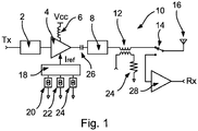
- FIG 1 shows a block diagram of a radio frequency front end 10 (hereinafter “front end” or “RFFE”), according to an embodiment of this disclosure.
- RFFE radio frequency front end 10
- the RFFE 10 includes an antenna 16, which may be used to transmit and receive radio frequency signals.
- a switch 14 may be provided to route the transmitted and received signals within the RFFE 10. As shown in Figure 1 , the switch 14 may be set to connect the antenna 16 to a transmit path (Tx) of the RFFE 10. Alternatively, the switch 14 may be set to connect the antenna to a receive path (Rx) of the RFFE 10.
- the receive path may include a low noise amplifier 28 for amplifying the received radio frequency signals.
- the RFFE 10 includes a power amplifier 4.
- the power amplifier 4 may include a transistor, such as a bipolar junction transistor for field effect transistor for amplifying an input signal to be transmitted by the antenna 16.
- the power amplifier 4 may be powered by supply voltage V cc .
- Inductance 6 provides an RF choke, which isolates the DC from the RF signal, and resonates with the output capacitance of the transistor in the power amplifier 4, so as to provide a resistive load at the collector of the transistor.
- the transmit path also includes a coupler 12 for coupling the amplified signal to the antenna 16.
- the coupler 12 may comprise an inductor.
- the transmit path may further include a capacitance 26, an input impedance matching network 2 and an output impedance matching network 8.
- the operation of the power amplifier may, in accordance with embodiments of this disclosure, be controlled using a reference current I ref .
- I ref may be used to bias the transistor of the power amplifier 4, so as to maintaining the transistor in a linear operating region.
- the reference current I ref may be used to correct for static and dynamic temperature effects in the power amplifier 4.
- the RFFE 10 includes circuitry for producing the reference current I ref .
- This circuitry may include a number of current mirrors 18, which can receive and process a number of input currents to generate I ref .
- An output of the current mirrors may be coupled to the power amplifier 4, so as to provide the reference current I ref to the power amplifier 4.
- the input currents which are used by the current mirrors 18 to produce the reference current I ref , include a first correction current I ptat , which is proportional to an absolute, static temperature of a semiconductor die including the transistor. Accordingly, the first correction current I ptat may allow the static temperature of the transistor to be factored in to the generation of the reference current I ref .
- the first correction current I ptat may be generated by a first current source 20.
- the input currents also include a second correction current I ptdt .
- the second correction current I ptdt is proportional to a change in temperature of the part of the semiconductor die in which the transistor is located. Accordingly, the second correction current I ptdt may allow changes in temperature of the part of the semiconductor die near the transistor to be factored in to the generation of the reference current I ref .
- the second correction current I ptdt may be generated by a second current source 22.
- the input currents also include a gain selection current I 0 .
- the gain selection current I 0 may be selected in accordance with an operational mode (e.g. required gain level) of the power amplifier 4.
- the gain selection current I 0 may be generated by a third current source 24.
- the gain selection current I 0 may itself be used in the generation of the first and second correction currents I ptat , I ptdt .
- FIG. 2 shows, in more detail, circuitry 300 for producing the reference current I ref according to an embodiment of this disclosure.
- the circuit 300 includes a number of subcircuits.
- the circuitry 300 includes a static temperature sub-circuit 40 and a dynamic temperature sub-circuit 50.
- Each sub-circuit 40, 50 and further sub-circuitry thereof, may produce a respective contribution to the reference current I ref .
- the static temperature sub-circuit 40 is configured to use the first correction current I ptat and the gain selection current I 0 to produce a contribution to the reference current I ref associated with the absolute, static temperature of the semiconductor die incorporating the transistor of the power amplifier 4.
- the static temperature sub-circuit 40 includes a first sub-circuit 42 and a second sub-circuit 44.
- the dynamic temperature sub-circuit 50 is configured to use the first correction current I ptat and the second current I ptdt to produce a contribution to the reference current associated with a change in temperature of the part of the semiconductor die in which the transistor of the power amplifier 4 is located.
- the dynamic temperature sub-circuit 50 in this embodiment includes circuitry 52 for producing an uncorrected contribution to the reference current associated with the change in temperature of the part of the semiconductor die in which the transistor of the power amplifier 4 is located from the second correction current I ptdt .
- the dynamic temperature sub-circuit 50 in this embodiment also includes circuitry 54 for removing a static part from the contribution to I ref produced by the dynamic temperature sub-circuit 50.
- the circuitry 54 uses the first correction current I ptat to make this correction.
- the output (represented by the node 302) of the circuitry 300 is used to provide the reference current I ref to the power amplifier 4.
- the node 302 is connected to the output(s) of the static temperature sub-circuit 40 and the dynamic temperature sub-circuit 50 for producing I ref .
- I ref is provided to the input of a current mirror 30 comprising a pair of transistors 32, 34.
- the emitters of each transistor 32, 34 are connected to the power amplifier supply voltage V cc .
- the collector of the transistor 32 is coupled to the node 302 to receive I ref .
- the bases of each transistor 32, 34 are coupled together, and are further coupled to the node 302 (the bases receive I ref / ⁇ , where ⁇ is the PNP current gain).
- the output of the current mirror 30 is provided to a replica transistor at 200.
- the replica transistor designates here a diode-mounted transistor, which forms with the power cell a last current mirror for a good collector current control. In this way, the collector current is an image of I ref .
- A, B and ⁇ are constants
- T die is the absolute, static temperature of the semiconductor die in which the transistor of the power amplifier 4 is provided
- T PA is a temperature to which the temperature of the part of the semiconductor die in which the transistor of the power amplifier 4 is located changes during operation of the transistor (accordingly, the associated change of temperature of the power amplifier is given by (T PA - T die )).
- the junction temperature of the transistor may be considered to be substantially equal to T PA .
- the various parts of the circuitry 300 in Figure 2 may be allocated the task of producing contributions corresponding to respective parts of the expression for I ref shown above.
- dtT die T PA - T die , and corresponds to the change in temperature of the part of the semiconductor die in which the transistor of the power amplifier 4 is located during operation of the transistor, as noted above.
- I ptdt is proportional to the aforementioned change in temperature, but also includes a contribution corresponding the absolute, static temperature T die .
- the circuit of Figure 2 may use control codes to control a number of current mirrors provided within the static temperature sub-circuit 40 and the dynamic temperature sub-circuit 50 for the generation of the various contributions to the reference current I ref .
- the first sub-circuit 42, second sub-circuit 44, and circuitry 52 may include current mirrors that comprise a plurality of field effect transistors (e.g. NMOS or PMOS) connected in parallel, with gates that are connected to receive a respective bit of the control code for that current mirror.
- the circuitry 54 may include a current mirror that comprise a plurality of field effect transistors (e.g. NMOS or PMOS) connected in parallel, with gates that are connected to receive a respective bit of the control code for that current mirror.
- the control codes may be generated by digital circuitry of the circuitry 300 and provided to the current mirrors. In one example implementation, 0V or 2.5V values may be given to each control code depending on the targeted correction or gain selection. These voltages may be applied to the gate of NMOS or PMOS transistors of the current mirrors to control the current flowing within the bias circuitry.
- I ref A . T die + B + ⁇ . T PA ⁇ T die the operation of the various parts of the circuit in Figure 2 for producing the various contributions to the reference current I ref will now be described.
- the static temperature sub-circuit 40 allows the contribution A.T die + B to I ref to be produced.
- the first sub-circuit 42 includes a current mirror which uses first reference current I ptat to produce the contribution A.T die
- the second sub-circuit 44 includes a current mirror which uses the gain selection current I 0 to produce the contribution B.
- the outputs of the first sub-circuit 42 and second sub-circuit 44 of the static temperature sub-circuit 40 are summed at the output of the static temperature sub-circuit 40 presented at node 302.
- the first reference current I ptat may be produced from a bandgap voltage by the current source for I ptat shown in Figure 2 .
- the first sub-circuit 42 of the static temperature sub-circuit 40 controls and amplifies the first reference current I ptat using the current mirror S x shown in Figure 2 .
- the circuitry 300 may be operable to use the code word X to control the current mirror S x in the first cub-circuit 42.
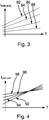
- the output of the current mirror S x (corresponding to the first reference current I ptat , amplified by the current mirror S x ), as a function of the static temperature T 0 is shown in Figure 3 .
- Each slope 82, 84, 86, 88 in Figure 3 corresponds to a different value of the constant A.
- the second sub-circuit 44 of the static temperature sub-circuit 40 uses the current mirror S x and the current mirror S z to control and amplify the gain selection current I 0 .
- the circuitry 300 may be operable to use the code word X to control the current mirror S x in the second cub-circuit 44 and the code word Z to control the current mirror S z to produce the contribution B from the gain selection current I 0 .
- the control code Z in this embodiment is exclusively dedicated to the gain selection current (for a multi-mode power amplifier 4 operable at different gain levels).
- the second sub-circuit 44 acts to bring each slope 82, 84, 86, 88 shown in Figure 3 back to the same level, thereby correcting A.T die , as produced by the first sub-circuit 42, for B, as produced by the second sub-circuit 44.
- the corrected slopes 92, 94, 96, 98, corresponding to A.T die + B, are shown in Figure 4 .
- the output of the static temperature sub-circuit 40 is a current that is proportional to the static temperature of the die (T die ), and allows errors (the error vector magnitude (EVM)) associated with slow thermal constant and the static temperature of the die incorporating the transistor of the power amplifier 4 to be compensated for.
- the static temperature sub-circuit 40 may accordingly compensate for changes in ambient temperature of the die, as opposed to the typically faster changes in temperature caused by the operation of the transistor of the power amplifier 4 in the vicinity of the transistor.
- the dynamic temperature sub-circuit 50 in this embodiment includes circuitry 52 for producing an uncorrected contribution to the reference current associated with the change in temperature of the part of the semiconductor die in which the transistor of the power amplifier 4 is located during operation of the transistor from the second correction current I ptdt , and circuitry 54 for removing a static part from the contribution to I ref produced by the dynamic temperature sub-circuit 50.
- the circuitry 52 includes current mirror S y , which controls and amplifies the second reference current I ptdt to produce a contribution to I ref corresponding to ⁇ T PA .
- the circuitry 300 may be operable to use the code word Y to control the current mirror S y in the circuitry 52 for producing ⁇ T PA from the second reference current I ptdt .
- the circuitry 54 includes a (e.g. PMOS) current mirror S y , which controls and amplifies the first reference current I ptat to produce a contribution to I ref corresponding to - ⁇ T die .
- a (e.g. PMOS) current mirror S y which controls and amplifies the first reference current I ptat to produce a contribution to I ref corresponding to - ⁇ T die .
- I ptdt a . T die + dtT die + b on T die to be removed.
- the circuitry 300 may be operable to use the code word Y to control the current mirror S y in the circuitry 54 for producing - ⁇ T die from the first reference current I ptat .
- the outputs of the circuitry 52 and the circuitry 54 of the dynamic temperature sub-circuit 50 are summed at the output of the dynamic temperature sub-circuit 50 presented at node 302.
- I ref ZS z b ⁇ XS x b + XS x a .
- T die + b dtT die + b ⁇ YS y a .
- I ptat and I ptdt include b (where b is equal to the gain selection current I 0 ), and I ptat and I ptdt are thus at least in part determined by the gain selection current I 0 .
- Figure 5 shows a circuit for producing the first reference current I ptat from the gain selection current I 0 .
- Figure 6 shows a circuit for producing the second reference current I ptdt from the gain selection current I 0 .
- the circuit of Figure 5 includes a current mirror formed by transistors 64, 66.
- the circuit of Figure 5 also includes a current source 62 which is operable to output a current based on a bandgap voltage reference.
- the circuit of Figure 5 further includes a pair of cross coupled transistors 72, 74 (e.g. NPN bipolar transistors).
- Each transistor in the circuit of Figure 5 includes a first current terminal, a second current terminal and a control terminal.
- the current terminals may for instance be the collector and the emitter of a bipolar junction transistor, and the control terminal may be the base.
- the control terminal of the transistor 64 is coupled to the control terminal of the transistor 66.
- the current source 62 is coupled to a first current terminal (e.g. the collector) of the transistor 64 and to the control terminals of the transistors 64, 66.
- the second current terminal (e.g. the emitter) of the transistor 64 is coupled to the first current terminal (e.g. the collector) of the transistor 72.
- the second current terminal (e.g. the emitter) of the transistor 66 is coupled to the first current terminal (e.g. the collector) of the second transistor 74.
- the control terminal of the transistor 72 is coupled to the first current terminal (e.g. the collector) of the transistor 74.
- the control terminal of the transistor 74 is coupled to the first current terminal (e.g. the collector) of the transistor 72.
- the second current terminal (e.g. the emitter) of the transistor 72 is coupled to a reference potential, typically ground.
- the second current terminal (e.g. the emitter) of the transistor 74 is coupled to the reference potential (typically ground) via a resistor 76.
- the circuit shown in Figure 6 is substantially the same as the circuit shown in Figure 5 (note that the features 162, 164, 166, 170, 172, 174, 176, 178 in Figure 6 correspond to the features 62, 64, 66, 70, 72, 74, 76, 78 in Figure 5 , respectively). However, while the cross connected pair of transistors 72, 74 (highlighted in the box 70) in Figure 5 is held at temperature of the die T die (e.g.
- the cross connected pair of transistors 172, 174 (highlighted in the box 170) in Figure 6 is held at temperature of the part of the semiconductor die in which the transistor of the power amplifier 4 is located T PA , which may be the junction temperature of the transistor of the power amplifier 4.
- T PA which may be the junction temperature of the transistor of the power amplifier 4.
- the placing of the transistors 172, 174 at T PA allows the circuit of Figure 6 to track changes in temperature in the vicinity of the transistor of the power amplifier 4 during operation of the transistor, thereby to act as a current source for outputting (at node 178) the second reference current I ptdt .
- the temperature correction circuit includes a first current source circuit operable to provide a first correction current proportional to an absolute temperature of a semiconductor die including the transistor.
- the temperature correction circuit also includes a second current source circuit operable to provide a second correction current proportional to a change in temperature of a part of the semiconductor die in which the transistor is located during operation of the transistor.
- the temperature correction circuit further includes a third current source circuit operable to provide a gain selection current.
- the temperature correction circuit also includes circuitry for producing a reference current from the first and second correction currents and the gain current.
- the temperature correction circuit further includes an output for providing the reference current to the transistor.
Landscapes
- Engineering & Computer Science (AREA)
- Power Engineering (AREA)
- Physics & Mathematics (AREA)
- Nonlinear Science (AREA)
- Microelectronics & Electronic Packaging (AREA)
- Amplifiers (AREA)
Abstract
Description
- The present specification relates to a temperature correction circuit for maintaining a transistor of a power amplifier in a linear operating region. The present specification also relates to a method of operating a power amplifier.
- Traditionally, static Error Vector Magnitude (EVM) calculations for power amplifiers have been based on amplitude-to-amplitude modulation (AM/AM) and amplitude-to-phase modulation (AM/PM) distortions and are proportional mainly to Pout/(Icq 2.Rl), where Pout is the output power of the power amplifier, Icq is the quiescent current of the power amplifier and Ri is the load impendence.
- However, this type of calculation does not capture the dynamic thermal behaviour of the power amplifier, which may be important to consider, especially in Time Division Duplex (TDD) systems and flip chip packages.
- The Dynamic Error Vector Magnitude (DEVM) is directly dependent on power gain variation. In wide temperature range bipolar power amplifiers, the power gain stabilization becomes important when targeting low DEVM levels.
- Aspects of the present disclosure are set out in the accompanying independent and dependent claims. Combinations of features from the dependent claims may be combined with features of the independent claims as appropriate and not merely as explicitly set out in the claims.
- According to an aspect of the present disclosure, there is provided a temperature correction circuit for maintaining a transistor of a power amplifier in a linear operating region of said transistor, the temperature correction circuit comprising:
- a first current source circuit operable to provide a first correction current proportional to an absolute, static temperature of a semiconductor die including said transistor;
- a second current source circuit operable to provide a second correction current proportional to a change in temperature of a part of said semiconductor die in which the transistor is located during operation of the transistor;
- a third current source circuit operable to provide a gain selection current;
- circuitry for producing a reference current from said first and second correction currents and said gain current; and
- an output for providing said reference current to said transistor.
- According to another aspect of the present disclosure, there is provided a method of operating a power amplifier, the method comprising:
- providing a gain selection current;
- providing a first correction current proportional to an absolute temperature of a semiconductor die including a transistor of said power amplifier;
- providing a second correction current proportional to a change in temperature of a part of said semiconductor die in which the transistor is located during operation of the transistor;
- producing a reference current from said first and second correction currents and said gain current; and
- providing said reference current to said transistor for maintaining said transistor in a linear operating region.
- A temperature correction circuit and method according to embodiments of this disclosure can allow the operation of a power amplifier to be corrected for static and dynamic temperature variations. This may be achieved using a single reference current.
- The circuitry for producing a reference current may include a static temperature sub-circuit configured to use the first correction current and the gain selection current to produce a contribution to the reference current associated with the absolute, static temperature of the die.
- The circuitry for producing a reference current may include a dynamic temperature sub-circuit configured to use the first correction current and the second current to produce a contribution to the reference current associated with the change in temperature of the part of the semiconductor die in which the transistor is located.
- The separate provision of a static temperature sub-circuit and a dynamic temperature sub-circuit may allow the static and dynamic contributions to the reference current to be produced separately, in a manner in which the dynamic correction does not affect the static correction, and vice versa.
- The dynamic temperature sub-circuit may include:
- circuitry for producing the contribution to the reference current associated with the change in temperature of the part of the semiconductor die in which the transistor is located from the second correction current; and
- circuitry for removing a static part from the contribution using the first correction current.
- The static temperature sub-circuit may include one or more programmable current mirrors for producing the contribution to the reference current associated with the absolute, static temperature of the die.
- The dynamic temperature sub-circuit may include one or more programmable current mirrors for producing the contribution to the reference current associated with the change in temperature of the part of the semiconductor die in which the transistor is located.
- The temperature correction circuit may be configured to use one or more code words for controlling the current mirrors to produce the contributions to the reference current. These control codes may be provided by digital circuitry of the temperature correction circuit.
- The reference current may be suitable for biasing the transistor of the power amplifier.
- The temperature correction circuit may be configured to determine the gain selection current according to a gain mode of the power amplifier.
- The first current source circuit may include a current mirror, a current source operable to output a current based on a bandgap voltage reference, and a pair of cross coupled transistors located at a temperature of the die.
- The first current source circuit may include:
- a first transistor pair comprising:
- a first transistor having a first current terminal, a second current terminal and a control terminal; and
- a second transistor having a first current terminal, a second current terminal and a control terminal; and
- a second transistor pair comprising:
- a first transistor having a first current terminal, a second current terminal and a control terminal; and
- a second transistor having a first current terminal, a second current terminal and a control terminal; and
- the pair of cross coupled transistors of the first current source circuit comprises the second transistor pair;
- the control terminal of the first transistor of the first transistor pair is coupled to the control terminal of the second transistor of the first transistor pair,
- the current source is coupled to the first control terminal of the first transistor of the first transistor pair and to the control terminals of the first transistor and the second transistor of the first transistor pair,
- the second current terminal of the first transistor of the first transistor pair is coupled to the first current terminal of the first transistor of the second transistor pair,
- the second current terminal of the second transistor of the first transistor pair is coupled to the first current terminal of the second transistor of the second transistor pair,
- the control terminal of the first transistor of the second transistor pair is coupled to the first current terminal of the second transistor of the second transistor pair,
- the control terminal of the second transistor of the second transistor pair is coupled to the first current terminal of the first transistor of the second transistor pair,
- the second current terminal of the first transistor of the second transistor pair is coupled to ground, and
- the second current terminal of the second transistor of the second transistor pair is coupled to ground via a resistor.
- The second current source circuit may include a current mirror, a current source operable to output a current based on a bandgap voltage reference, and a pair of cross coupled transistors located at a temperature of a junction of the transistor of the power amplifier.
- The first current source circuit may include:
- a first transistor pair comprising:
- a first transistor having a first current terminal, a second current terminal and a control terminal; and
- a second transistor having a first current terminal, a second current terminal and a control terminal; and
- a second transistor pair comprising:
- a first transistor having a first current terminal, a second current terminal and a control terminal; and
- a second transistor having a first current terminal, a second current terminal and a control terminal; and
- the pair of cross coupled transistors of the second current source circuit comprises the second transistor pair;
- the control terminal of the first transistor of the first transistor pair is coupled to the control terminal of the second transistor of the first transistor pair,
- the current source is coupled to the first current terminal of the first transistor of the first transistor pair and to the control terminals of the first transistor and the second transistor of the first transistor pair,
- the second current terminal of the first transistor of the first transistor pair is coupled to the first current terminal of the first transistor of the second transistor pair,
- the second current terminal of the second transistor of the first transistor pair is coupled to the first current terminal of the second transistor of the second transistor pair,
- the control terminal of the first transistor of the second transistor pair is coupled to the first current terminal of the second transistor of the second transistor pair,
- the control terminal of the second transistor of the second transistor pair is coupled to the first current terminal of the first transistor of the second transistor pair,
- the second current terminal of the first transistor of the second transistor pair is coupled to ground, and
- the second current terminal of the second transistor of the second transistor pair is coupled to ground via a resistor.
- The power amplifier may be a Radio Frequency (RF) power amplifier.
- The power amplifier may be coupled to the output of the temperature correction circuit for providing the reference current to the transistor of the power amplifier.
- For the purposes of this disclosure "Radio Frequency" (RF) refers to frequencies typically in the range of, but not limited to 0.5 GHz ≤ f ≤ 100 GHz.
- Embodiments of this disclosure will be described hereinafter, by way of example only, with reference to the accompanying drawings in which like reference signs relate to like elements and in which:
-
Figure 1 shows a block diagram of an RF Front End, according to an embodiment of this disclosure; -
Figure 2 shows a circuit according to an embodiment of this disclosure; -
Figure 3 shows an output of a current mirror according to an embodiment of this disclosure; -
Figure 4 shows an output of a current mirror according to an embodiment of this disclosure; -
Figure 5 shows a circuit according to an embodiment of this disclosure; and -
Figure 6 shows a circuit according to an embodiment of this disclosure. - Embodiments of this disclosure are described in the following with reference to the accompanying drawings.
-
Figure 1 shows a block diagram of a radio frequency front end 10 (hereinafter "front end" or "RFFE"), according to an embodiment of this disclosure. - The
RFFE 10 includes anantenna 16, which may be used to transmit and receive radio frequency signals. Aswitch 14 may be provided to route the transmitted and received signals within theRFFE 10. As shown inFigure 1 , theswitch 14 may be set to connect theantenna 16 to a transmit path (Tx) of theRFFE 10. Alternatively, theswitch 14 may be set to connect the antenna to a receive path (Rx) of theRFFE 10. The receive path may include alow noise amplifier 28 for amplifying the received radio frequency signals. - The features in the transmit path of the
RFFE 10 will now be described. - The
RFFE 10 includes apower amplifier 4. Thepower amplifier 4 may include a transistor, such as a bipolar junction transistor for field effect transistor for amplifying an input signal to be transmitted by theantenna 16. Thepower amplifier 4 may be powered by supply voltage Vcc. Inductance 6 provides an RF choke, which isolates the DC from the RF signal, and resonates with the output capacitance of the transistor in thepower amplifier 4, so as to provide a resistive load at the collector of the transistor. The transmit path also includes acoupler 12 for coupling the amplified signal to theantenna 16. Thecoupler 12 may comprise an inductor. The transmit path may further include acapacitance 26, an inputimpedance matching network 2 and an outputimpedance matching network 8. - The operation of the power amplifier may, in accordance with embodiments of this disclosure, be controlled using a reference current Iref. Iref may be used to bias the transistor of the
power amplifier 4, so as to maintaining the transistor in a linear operating region. In particular, the reference current Iref may be used to correct for static and dynamic temperature effects in thepower amplifier 4. - The
RFFE 10 includes circuitry for producing the reference current Iref. This circuitry may include a number ofcurrent mirrors 18, which can receive and process a number of input currents to generate Iref. An output of the current mirrors may be coupled to thepower amplifier 4, so as to provide the reference current Iref to thepower amplifier 4. - The input currents, which are used by the
current mirrors 18 to produce the reference current Iref, include a first correction current Iptat, which is proportional to an absolute, static temperature of a semiconductor die including the transistor. Accordingly, the first correction current Iptat may allow the static temperature of the transistor to be factored in to the generation of the reference current Iref. The first correction current Iptat may be generated by a firstcurrent source 20. - During operation of the transistor of the
power amplifier 4, a part of the semiconductor die in the vicinity of the transistor may change in temperature. Typically, the operation of the transistor will heat up this part of the semiconductor die, and conversely this part of the semiconductor die may cool down again when the transistor operates less or ceases to operate. To account for these changes in temperature, the input currents also include a second correction current Iptdt. The second correction current Iptdt is proportional to a change in temperature of the part of the semiconductor die in which the transistor is located. Accordingly, the second correction current Iptdt may allow changes in temperature of the part of the semiconductor die near the transistor to be factored in to the generation of the reference current Iref. The second correction current Iptdt may be generated by a secondcurrent source 22. - The input currents also include a gain selection current I0. The gain selection current I0 may be selected in accordance with an operational mode (e.g. required gain level) of the
power amplifier 4. The gain selection current I0 may be generated by a thirdcurrent source 24. The gain selection current I0 may itself be used in the generation of the first and second correction currents Iptat, Iptdt. -
Figure 2 shows, in more detail,circuitry 300 for producing the reference current Iref according to an embodiment of this disclosure. Thecircuit 300 includes a number of subcircuits. In particular, thecircuitry 300 includes astatic temperature sub-circuit 40 and adynamic temperature sub-circuit 50. Each sub-circuit 40, 50 and further sub-circuitry thereof, may produce a respective contribution to the reference current Iref. - The
static temperature sub-circuit 40 is configured to use the first correction current Iptat and the gain selection current I0 to produce a contribution to the reference current Iref associated with the absolute, static temperature of the semiconductor die incorporating the transistor of thepower amplifier 4. Thestatic temperature sub-circuit 40 includes afirst sub-circuit 42 and asecond sub-circuit 44. - The
dynamic temperature sub-circuit 50 is configured to use the first correction current Iptat and the second current Iptdt to produce a contribution to the reference current associated with a change in temperature of the part of the semiconductor die in which the transistor of thepower amplifier 4 is located. - The
dynamic temperature sub-circuit 50 in this embodiment includescircuitry 52 for producing an uncorrected contribution to the reference current associated with the change in temperature of the part of the semiconductor die in which the transistor of thepower amplifier 4 is located from the second correction current Iptdt. Thedynamic temperature sub-circuit 50 in this embodiment also includescircuitry 54 for removing a static part from the contribution to Iref produced by thedynamic temperature sub-circuit 50. Thecircuitry 54 uses the first correction current Iptat to make this correction. - As shown in
Figure 2 , the output (represented by the node 302) of thecircuitry 300 is used to provide the reference current Iref to thepower amplifier 4. Note that thenode 302 is connected to the output(s) of thestatic temperature sub-circuit 40 and the dynamic temperature sub-circuit 50 for producing Iref. In this embodiment, Iref is provided to the input of acurrent mirror 30 comprising a pair oftransistors transistor transistor 32 is coupled to thenode 302 to receive Iref. The bases of eachtransistor current mirror 30 is provided to a replica transistor at 200. The replica transistor designates here a diode-mounted transistor, which forms with the power cell a last current mirror for a good collector current control. In this way, the collector current is an image of Iref. - The mathematics of the generation of the reference current Iref will now be described.
- Reference current Iref may be expressed as:

power amplifier 4 is provided, and TPA is a temperature to which the temperature of the part of the semiconductor die in which the transistor of thepower amplifier 4 is located changes during operation of the transistor (accordingly, the associated change of temperature of the power amplifier is given by (TPA - Tdie)). Note that the junction temperature of the transistor may be considered to be substantially equal to TPA. As will be described in more detail below, the various parts of thecircuitry 300 inFigure 2 (in particular thestatic temperature sub-circuit 40, thedynamic temperature sub-circuit 50 and the sub circuitry thereof) may be allocated the task of producing contributions corresponding to respective parts of the expression for Iref shown above. - The first reference current Iptat may be expressed as:

- The second reference current Iptdt may be expressed as:

power amplifier 4 is located during operation of the transistor, as noted above. Note that Iptdt is proportional to the aforementioned change in temperature, but also includes a contribution corresponding the absolute, static temperature Tdie. - The gain selection current I0 may be expressed as:

power amplifier 4. In some embodiments, the gain selection current I0 may be around 50µA. - The circuit of
Figure 2 may use control codes to control a number of current mirrors provided within thestatic temperature sub-circuit 40 and the dynamic temperature sub-circuit 50 for the generation of the various contributions to the reference current Iref. In the present embodiment, thefirst sub-circuit 42, second sub-circuit 44, andcircuitry 52 may include current mirrors that comprise a plurality of field effect transistors (e.g. NMOS or PMOS) connected in parallel, with gates that are connected to receive a respective bit of the control code for that current mirror. In the present embodiment, thecircuitry 54 may include a current mirror that comprise a plurality of field effect transistors (e.g. NMOS or PMOS) connected in parallel, with gates that are connected to receive a respective bit of the control code for that current mirror. - The control codes may be generated by digital circuitry of the
circuitry 300 and provided to the current mirrors. In one example implementation, 0V or 2.5V values may be given to each control code depending on the targeted correction or gain selection. These voltages may be applied to the gate of NMOS or PMOS transistors of the current mirrors to control the current flowing within the bias circuitry. - In
Figure 2 : - Sx is the ratio of the current mirrors in the static temperature sub-circuit 40 for generating A.Tdie + B;
- Sy is the ratio of the current mirrors in the dynamic temperature sub-circuit 50 for generating α[TPA - Tdie];
- X is a control code to control a current mirror in the static temperature sub-circuit 40 (more particularly in the first sub-circuit 42 to be described below) for selection of a Tdie slope, corresponding to the value of the constant A (for the static error vector magnitude (EVM) temperature correction);
-
X is a control code to control a current mirror in the static temperature sub-circuit 40 (more particularly in the second sub-circuit 44 to be described below) for handling the current mirror of the current I0; - Y is a control code to control a current mirror in the dynamic temperature sub-circuit 50 (more particularly in the
circuitry 52 to be described below) for selection of a dtTdie slope, corresponding to the value of the constant a (for the dynamic error vector magnitude (EVM) temperature correction); -
Y is a control code to control a current mirror in the dynamic temperature sub-circuit 50 (more particularly in thecircuitry 54 to be described below) to perform a subtraction of the static part from the contribution to Iref produced by thedynamic temperature sub-circuit 50; and - Z is a control code to control a current mirror in the static temperature sub-circuit 40 (more particularly in the second sub-circuit 44 to be described below) for selection the Iref level, corresponding to the value of the constant B.
- Recalling that:

Figure 2 for producing the various contributions to the reference current Iref will now be described. In this respect, note that the reference current may also be written as: Iref = A.Tdie + α.dtTdie + B. - In
Figure 2 , thestatic temperature sub-circuit 40 allows the contribution A.Tdie + B to Iref to be produced. In particular, as shown inFigure 2 , thefirst sub-circuit 42 includes a current mirror which uses first reference current Iptat to produce the contribution A.Tdie, and thesecond sub-circuit 44 includes a current mirror which uses the gain selection current I0 to produce the contribution B. The outputs of thefirst sub-circuit 42 andsecond sub-circuit 44 of thestatic temperature sub-circuit 40 are summed at the output of thestatic temperature sub-circuit 40 presented atnode 302. - The first reference current Iptat may be produced from a bandgap voltage by the current source for Iptat shown in
Figure 2 . Thefirst sub-circuit 42 of thestatic temperature sub-circuit 40 controls and amplifies the first reference current Iptat using the current mirror Sx shown inFigure 2 . Thecircuitry 300 may be operable to use the code word X to control the current mirror Sx in the first cub-circuit 42. The output of the current mirror Sx (corresponding to the first reference current Iptat, amplified by the current mirror Sx), as a function of the static temperature T0 is shown inFigure 3 . Eachslope Figure 3 corresponds to a different value of the constant A. - The
second sub-circuit 44 of thestatic temperature sub-circuit 40 uses the current mirror Sx and the current mirror Sz to control and amplify the gain selection current I0. Thecircuitry 300 may be operable to use the code wordX to control the current mirror Sx in the second cub-circuit 44 and the code word Z to control the current mirror Sz to produce the contribution B from the gain selection current I0. Note that the control code Z in this embodiment is exclusively dedicated to the gain selection current (for amulti-mode power amplifier 4 operable at different gain levels). - The second sub-circuit 44 acts to bring each
slope Figure 3 back to the same level, thereby correcting A.Tdie, as produced by thefirst sub-circuit 42, for B, as produced by thesecond sub-circuit 44. The corrected slopes 92, 94, 96, 98, corresponding to A.Tdie + B, are shown inFigure 4 . As described herein, the output of thestatic temperature sub-circuit 40 is a current that is proportional to the static temperature of the die (Tdie), and allows errors (the error vector magnitude (EVM)) associated with slow thermal constant and the static temperature of the die incorporating the transistor of thepower amplifier 4 to be compensated for. Thestatic temperature sub-circuit 40 may accordingly compensate for changes in ambient temperature of the die, as opposed to the typically faster changes in temperature caused by the operation of the transistor of thepower amplifier 4 in the vicinity of the transistor. - As noted previously, the
dynamic temperature sub-circuit 50 in this embodiment includescircuitry 52 for producing an uncorrected contribution to the reference current associated with the change in temperature of the part of the semiconductor die in which the transistor of thepower amplifier 4 is located during operation of the transistor from the second correction current Iptdt, andcircuitry 54 for removing a static part from the contribution to Iref produced by thedynamic temperature sub-circuit 50. In particular, thecircuitry 52 includes current mirror Sy, which controls and amplifies the second reference current Iptdt to produce a contribution to Iref corresponding to αTPA. Thecircuitry 300 may be operable to use the code word Y to control the current mirror Sy in thecircuitry 52 for producing αTPA from the second reference current Iptdt. - The
circuitry 54 includes a (e.g. PMOS) current mirror Sy, which controls and amplifies the first reference current Iptat to produce a contribution to Iref corresponding to - αTdie. This allows the dependency of the expression
circuitry 300 may be operable to use the code wordY to control the current mirror Sy in thecircuitry 54 for producing -αTdie from the first reference current Iptat. - The outputs of the
circuitry 52 and thecircuitry 54 of thedynamic temperature sub-circuit 50 are summed at the output of thedynamic temperature sub-circuit 50 presented atnode 302. - To summarise, the above stated expression for the reference current Iref, namely

circuitry 300 as:
- • B = ZSzb,
- • A = XSxa, and
- • α = YSya.
- As mentioned previously, the expressions for Iptat and Iptdt shown above includes b (where b is equal to the gain selection current I0), and Iptat and Iptdt are thus at least in part determined by the gain selection current I0.
Figure 5 shows a circuit for producing the first reference current Iptat from the gain selection current I0.Figure 6 shows a circuit for producing the second reference current Iptdt from the gain selection current I0. - The circuit of
Figure 5 includes a current mirror formed bytransistors Figure 5 also includes acurrent source 62 which is operable to output a current based on a bandgap voltage reference. The circuit ofFigure 5 further includes a pair of cross coupledtransistors 72, 74 (e.g. NPN bipolar transistors). Each transistor in the circuit ofFigure 5 includes a first current terminal, a second current terminal and a control terminal. The current terminals may for instance be the collector and the emitter of a bipolar junction transistor, and the control terminal may be the base. - The control terminal of the
transistor 64 is coupled to the control terminal of thetransistor 66. Thecurrent source 62 is coupled to a first current terminal (e.g. the collector) of thetransistor 64 and to the control terminals of thetransistors transistor 64 is coupled to the first current terminal (e.g. the collector) of thetransistor 72. The second current terminal (e.g. the emitter) of thetransistor 66 is coupled to the first current terminal (e.g. the collector) of thesecond transistor 74. The control terminal of thetransistor 72 is coupled to the first current terminal (e.g. the collector) of thetransistor 74. The control terminal of thetransistor 74 is coupled to the first current terminal (e.g. the collector) of thetransistor 72. The second current terminal (e.g. the emitter) of thetransistor 72 is coupled to a reference potential, typically ground. The second current terminal (e.g. the emitter) of thetransistor 74 is coupled to the reference potential (typically ground) via aresistor 76. - The circuit shown in
Figure 6 is substantially the same as the circuit shown inFigure 5 (note that thefeatures Figure 6 correspond to thefeatures Figure 5 , respectively). However, while the cross connected pair oftransistors 72, 74 (highlighted in the box 70) inFigure 5 is held at temperature of the die Tdie (e.g. by placing thetransistors transistors 172, 174 (highlighted in the box 170) inFigure 6 is held at temperature of the part of the semiconductor die in which the transistor of thepower amplifier 4 is located TPA, which may be the junction temperature of the transistor of thepower amplifier 4. The placing of thetransistors Figure 5 to act as a current source for outputting (at node 78) the first reference current Iptat. The placing of thetransistors Figure 6 to track changes in temperature in the vicinity of the transistor of thepower amplifier 4 during operation of the transistor, thereby to act as a current source for outputting (at node 178) the second reference current Iptdt. - Accordingly, there has been described a temperature correction circuit and method for maintaining a transistor of a power amplifier in a linear operating region of the transistor. The temperature correction circuit includes a first current source circuit operable to provide a first correction current proportional to an absolute temperature of a semiconductor die including the transistor. The temperature correction circuit also includes a second current source circuit operable to provide a second correction current proportional to a change in temperature of a part of the semiconductor die in which the transistor is located during operation of the transistor. The temperature correction circuit further includes a third current source circuit operable to provide a gain selection current. The temperature correction circuit also includes circuitry for producing a reference current from the first and second correction currents and the gain current. The temperature correction circuit further includes an output for providing the reference current to the transistor.
- Although particular embodiments of this disclosure have been described, it will be appreciated that many modifications/additions and/or substitutions may be made within the scope of the claims.
Claims (15)
- A temperature correction circuit for maintaining a transistor of a power amplifier in a linear operating region of said transistor, the temperature correction circuit comprising:a first current source circuit operable to provide a first correction current proportional to an absolute, static temperature of a semiconductor die including said transistor;a second current source circuit operable to provide a second correction current proportional to a change in temperature of a part of said semiconductor die in which the transistor is located during operation of the transistor;a third current source circuit operable to provide a gain selection current;circuitry for producing a reference current from said first and second correction currents and said gain current; andan output for providing said reference current to said transistor.
- The temperature correction circuit of claim 1, wherein the circuitry for producing a reference current comprises a static temperature sub-circuit configured to use said first correction current and said gain selection current to produce a contribution to the reference current associated with said absolute, static temperature of the die.
- The temperature correction circuit of claim 1 or claim 2, wherein the circuitry for producing a reference current comprises a dynamic temperature sub-circuit configured to use said first correction current and said second current to produce a contribution to the reference current associated with said change in temperature of said part of the semiconductor die in which the transistor is located.
- The temperature correction circuit of claim 3, wherein the dynamic temperature sub-circuit comprises:circuitry for producing said contribution to the reference current associated with said change in temperature of said part of the semiconductor die in which the transistor is located from the second correction current; andcircuitry for removing a static part from said contribution using the first correction current.
- The temperature correction circuit of any of claims 2 to 4, whereinthe static temperature sub-circuit includes one or more programmable current mirrors for producing the contribution to the reference current associated with said absolute, static temperature of the die; and/orthe dynamic temperature sub-circuit includes one or more programmable current mirrors for producing the contribution to the reference current associated with said change in temperature of said part of the semiconductor die in which the transistor is located.
- The temperature correction circuit of claim 5, wherein the temperature correction circuit is configured to use one or more code words for controlling the current mirrors to produce said contributions to the reference current.
- The temperature correction circuit of any preceding claim, wherein the reference current is for biasing the transistor of the power amplifier.
- The temperature correction circuit of any preceding claim, configured to determine the gain selection current according to a gain mode of the power amplifier.
- The temperature correction circuit of any preceding claim, wherein the first current source circuit includes a current mirror, a current source operable to output a current based on a bandgap voltage reference, and a pair of cross coupled transistors located at a temperature of said die.
- The temperature correction circuit of claim 9, wherein the first current source circuit comprises:a first transistor pair comprising:a first transistor having a first current terminal, a second current terminal and a control terminal; anda second transistor having a first current terminal, a second current terminal and a control terminal; anda second transistor pair comprising:wherein:a first transistor having a first current terminal, a second current terminal and a control terminal; anda second transistor having a first current terminal, a second current terminal and a control terminal; andsaid pair of cross coupled transistors of said first current source circuit comprises said second transistor pair;the control terminal of the first transistor of the first transistor pair is coupled to the control terminal of the second transistor of the first transistor pair,the current source is coupled to the first current terminal of the first transistor of the first transistor pair and to the control terminals of the first transistor and the second transistor of the first transistor pair,the second current terminal of the first transistor of the first transistor pair is coupled to the first current terminal of the first transistor of the second transistor pair,the second current terminal of the second transistor of the first transistor pair is coupled to the first current terminal of the second transistor of the second transistor pair,the control terminal of the first transistor of the second transistor pair is coupled to the first current terminal of the second transistor of the second transistor pair,the control terminal of the second transistor of the second transistor pair is coupled to the first current terminal of the first transistor of the second transistor pair,the second current terminal of the first transistor of the second transistor pair is coupled to ground, andthe second current terminal of the second transistor of the second transistor pair is coupled to ground via a resistor.
- The temperature correction circuit of any preceding claim, wherein the second current source circuit includes a current mirror, a current source operable to output a current based on a bandgap voltage reference, and a pair of cross coupled transistors located at a temperature of a junction of said transistor of said power amplifier.
- The temperature correction circuit of claim 11, wherein the first current source circuit comprises:a first transistor pair comprising:a first transistor having a first current terminal, a second current terminal and a control terminal; anda second transistor having a first current terminal, a second current terminal and a control terminal; anda second transistor pair comprising:a first transistor having a first current terminal, a second current terminal and a control terminal; anda second transistor having a first current terminal, a second currentterminal and a control terminal; andwherein:said pair of cross coupled transistors of said second current source circuit comprises said second transistor pair;the control terminal of the first transistor of the first transistor pair is coupled to the control terminal of the second transistor of the first transistor pair,the current source is coupled to the first control terminal of the first transistor of the first transistor pair and to the control terminals of the first transistor and the second transistor of the first transistor pair,the second current terminal of the first transistor of the first transistor pair is coupled to the first current terminal of the first transistor of the second transistor pair,the second current terminal of the second transistor of the first transistor pair is coupled to the first current terminal of the second transistor of the second transistor pair,the control terminal of the first transistor of the second transistor pair is coupled to the first current terminal of the second transistor of the second transistor pair,the control terminal of the second transistor of the second transistor pair is coupled to the first current terminal of the first transistor of the second transistor pair,the second current terminal of the first transistor of the second transistor pair is coupled to ground, andthe second current terminal of the second transistor of the second transistor pair is coupled to ground via a resistor.
- The temperature correction circuit of any preceding claim, wherein the power amplifier is a Radio Frequency (RF) power amplifier.
- The temperature correction circuit of any preceding claim and said power amplifier coupled to the output of the temperature correction circuit for providing the reference current to the transistor of the power amplifier.
- A method of operating a power amplifier, the method comprising:providing a gain selection current;providing a first correction current proportional to an absolute temperature of a semiconductor die including a transistor of said power amplifier;providing a second correction current proportional to a change in temperature of a part of said semiconductor die in which the transistor is located during operation of the transistor;producing a reference current from said first and second correction currents and said gain current; andproviding said reference current to said transistor for maintaining said transistor in a linear operating region.
Priority Applications (3)
| Application Number | Priority Date | Filing Date | Title |
|---|---|---|---|
| EP19305614.0A EP3739750B1 (en) | 2019-05-14 | 2019-05-14 | Temperature correction circuit and method of operating a power amplifier |
| US16/860,645 US11251752B2 (en) | 2019-05-14 | 2020-04-28 | Temperature correction circuit and method of operating a power amplifier |
| CN202010405244.3A CN111953307B (en) | 2019-05-14 | 2020-05-13 | Temperature correction circuit and method of operating a power amplifier |
Applications Claiming Priority (1)
| Application Number | Priority Date | Filing Date | Title |
|---|---|---|---|
| EP19305614.0A EP3739750B1 (en) | 2019-05-14 | 2019-05-14 | Temperature correction circuit and method of operating a power amplifier |
Publications (2)
| Publication Number | Publication Date |
|---|---|
| EP3739750A1 true EP3739750A1 (en) | 2020-11-18 |
| EP3739750B1 EP3739750B1 (en) | 2023-07-26 |
Family
ID=66685515
Family Applications (1)
| Application Number | Title | Priority Date | Filing Date |
|---|---|---|---|
| EP19305614.0A Active EP3739750B1 (en) | 2019-05-14 | 2019-05-14 | Temperature correction circuit and method of operating a power amplifier |
Country Status (3)
| Country | Link |
|---|---|
| US (1) | US11251752B2 (en) |
| EP (1) | EP3739750B1 (en) |
| CN (1) | CN111953307B (en) |
Families Citing this family (4)
| Publication number | Priority date | Publication date | Assignee | Title |
|---|---|---|---|---|
| CN111294004B (en) * | 2020-05-13 | 2020-08-28 | 锐石创芯(深圳)科技有限公司 | Gain compensation device and bias circuit device |
| CN113162564B (en) * | 2021-03-25 | 2023-05-26 | 成都知融科技有限公司 | CMOS power amplifier with temperature compensation function on chip |
| US12587144B2 (en) | 2023-05-08 | 2026-03-24 | Nxp Usa, Inc. | Power amplifier (PA) self-heating tracking for with self-heating time constant estimation |
| CN116633383B (en) * | 2023-07-18 | 2023-10-17 | 唯捷创芯(天津)电子技术股份有限公司 | Radio frequency front-end module for optimizing dynamic error vector amplitude and electronic equipment |
Citations (1)
| Publication number | Priority date | Publication date | Assignee | Title |
|---|---|---|---|---|
| US10230335B2 (en) * | 2016-09-30 | 2019-03-12 | Skyworks Solutions, Inc. | Temperature compensated power amplifier gain |
Family Cites Families (8)
| Publication number | Priority date | Publication date | Assignee | Title |
|---|---|---|---|---|
| US5396163A (en) * | 1991-03-13 | 1995-03-07 | Inco Limited | Battery charger |
| JP3479408B2 (en) * | 1996-04-23 | 2003-12-15 | アルプス電気株式会社 | AGC voltage correction circuit |
| US7342451B2 (en) * | 2005-08-05 | 2008-03-11 | Siemens Medical Soluitions Usa, Inc. | System for logarithmically controlling multiple variable gain amplifiers |
| JP5235025B2 (en) * | 2010-07-27 | 2013-07-10 | 旭化成エレクトロニクス株式会社 | Amplifier circuit |
| US9813027B2 (en) | 2013-12-31 | 2017-11-07 | Skyworks Solutions, Inc. | Devices and methods related to embedded sensors for dynamic error vector magnitude corrections |
| CN104682898B (en) * | 2015-02-15 | 2017-03-22 | 上海唯捷创芯电子技术有限公司 | Active bias circuit for power amplifier and communication equipment |
| KR102282192B1 (en) * | 2015-07-23 | 2021-07-27 | 삼성전자 주식회사 | Semiconductor device with mismatch detection and recovery circuit |
| GB201810227D0 (en) * | 2018-06-21 | 2018-08-08 | Nordic Semiconductor Asa | Oscillator circuits |
-
2019
- 2019-05-14 EP EP19305614.0A patent/EP3739750B1/en active Active
-
2020
- 2020-04-28 US US16/860,645 patent/US11251752B2/en active Active
- 2020-05-13 CN CN202010405244.3A patent/CN111953307B/en active Active
Patent Citations (1)
| Publication number | Priority date | Publication date | Assignee | Title |
|---|---|---|---|---|
| US10230335B2 (en) * | 2016-09-30 | 2019-03-12 | Skyworks Solutions, Inc. | Temperature compensated power amplifier gain |
Non-Patent Citations (3)
| Title |
|---|
| HUI DONG LEE ET AL: "A Wideband CMOS Variable Gain Amplifier With an Exponential Gain Control", IEEE TRANSACTIONS ON MICROWAVE THEORY AND TECHNIQUES, PLENUM, USA, vol. 55, no. 6, 1 June 2007 (2007-06-01), pages 1363 - 1373, XP011185145, ISSN: 0018-9480, DOI: 10.1109/TMTT.2007.896787 * |
| KENICHI AGAWA ET AL: "A 0.13 m CMOS Bluetooth EDR Transceiver with High Sensitivity over Wide Temperature Range and Immunity to Process Variation", IEICE TRANSACTIONS ON ELECTRONICS, INSTITUTE OF ELECTRONICS, TOKYO, JP, vol. E93C, no. 6, 1 June 2010 (2010-06-01), pages 803 - 811, XP001557243, ISSN: 0916-8524, DOI: 10.1587/TRANSELE.E93.C.803 * |
| OFIR DEGANI ET AL: "A 90nm CMOS PA module for 4G applications with embedded PVT gain compensation circuit", IEEE TOPICAL CONFERENCE ON POWER AMPLIFIERS FOR WIRELESS AND RADIO APPLICATIONS (PAWR); 15 -18 JANUARY 2012; SANTA CLARA, CA, IEEE, 15 January 2012 (2012-01-15), pages 25 - 28, XP032153870, ISBN: 978-1-4577-1119-0, DOI: 10.1109/PAWR.2012.6174913 * |
Also Published As
| Publication number | Publication date |
|---|---|
| US20200366246A1 (en) | 2020-11-19 |
| CN111953307B (en) | 2025-10-03 |
| US11251752B2 (en) | 2022-02-15 |
| CN111953307A (en) | 2020-11-17 |
| EP3739750B1 (en) | 2023-07-26 |
Similar Documents
| Publication | Publication Date | Title |
|---|---|---|
| US11251752B2 (en) | Temperature correction circuit and method of operating a power amplifier | |
| EP1744448B1 (en) | Radio frequency amplifiers | |
| US11456707B2 (en) | Power amplifier circuit | |
| US7696826B2 (en) | Temperature compensation of collector-voltage control RF amplifiers | |
| CN106357226B (en) | Power amplifier module | |
| EP1855379B1 (en) | Output power control of an RF amplifier | |
| US20100066433A1 (en) | Bias controller | |
| EP1580881B1 (en) | High-frequency power amplifier and communication apparatus | |
| CN116382402B (en) | Band gap reference voltage generating circuit and integrated circuit | |
| KR100247471B1 (en) | Agc voltage correction circuit | |
| US6486724B2 (en) | FET bias circuit | |
| US10432154B2 (en) | Regulation of an RF amplifier | |
| CN109842389B (en) | Radio frequency power amplifier and power control circuit thereof | |
| US7948319B2 (en) | Current-mirroring systems and methods | |
| EP1326328B1 (en) | High-frequency amplifier | |
| JP2021005818A (en) | Power amplification circuit | |
| US8779854B2 (en) | Variable gain amplifier circuit | |
| US9998080B2 (en) | Low voltage supply amplifier | |
| EP1601100A1 (en) | Transistor amplifying stage | |
| US20250286513A1 (en) | Voltage regulator to enable reduced memory effects in power amplifier | |
| US11764736B2 (en) | Bias compensation circuit of amplifier | |
| JP2024131165A (en) | Amplification circuit and system | |
| KR101983141B1 (en) | Bias circuit and amplifier using the same | |
| US20200389136A1 (en) | Power Amplifier Arrangement | |
| CN111030623A (en) | Adjustable gain amplifier for calibrating direct current offset |
Legal Events
| Date | Code | Title | Description |
|---|---|---|---|
| STAA | Information on the status of an ep patent application or granted ep patent |
Free format text: STATUS: UNKNOWN |
|
| PUAI | Public reference made under article 153(3) epc to a published international application that has entered the european phase |
Free format text: ORIGINAL CODE: 0009012 |
|
| STAA | Information on the status of an ep patent application or granted ep patent |
Free format text: STATUS: THE APPLICATION HAS BEEN PUBLISHED |
|
| AK | Designated contracting states |
Kind code of ref document: A1 Designated state(s): AL AT BE BG CH CY CZ DE DK EE ES FI FR GB GR HR HU IE IS IT LI LT LU LV MC MK MT NL NO PL PT RO RS SE SI SK SM TR |
|
| AX | Request for extension of the european patent |
Extension state: BA ME |
|
| STAA | Information on the status of an ep patent application or granted ep patent |
Free format text: STATUS: REQUEST FOR EXAMINATION WAS MADE |
|
| 17P | Request for examination filed |
Effective date: 20210518 |
|
| RBV | Designated contracting states (corrected) |
Designated state(s): AL AT BE BG CH CY CZ DE DK EE ES FI FR GB GR HR HU IE IS IT LI LT LU LV MC MK MT NL NO PL PT RO RS SE SI SK SM TR |
|
| STAA | Information on the status of an ep patent application or granted ep patent |
Free format text: STATUS: EXAMINATION IS IN PROGRESS |
|
| 17Q | First examination report despatched |
Effective date: 20220512 |
|
| GRAP | Despatch of communication of intention to grant a patent |
Free format text: ORIGINAL CODE: EPIDOSNIGR1 |
|
| STAA | Information on the status of an ep patent application or granted ep patent |
Free format text: STATUS: GRANT OF PATENT IS INTENDED |
|
| INTG | Intention to grant announced |
Effective date: 20230328 |
|
| GRAS | Grant fee paid |
Free format text: ORIGINAL CODE: EPIDOSNIGR3 |
|
| GRAA | (expected) grant |
Free format text: ORIGINAL CODE: 0009210 |
|
| STAA | Information on the status of an ep patent application or granted ep patent |
Free format text: STATUS: THE PATENT HAS BEEN GRANTED |
|
| AK | Designated contracting states |
Kind code of ref document: B1 Designated state(s): AL AT BE BG CH CY CZ DE DK EE ES FI FR GB GR HR HU IE IS IT LI LT LU LV MC MK MT NL NO PL PT RO RS SE SI SK SM TR |
|
| REG | Reference to a national code |
Ref country code: CH Ref legal event code: EP |
|
| REG | Reference to a national code |
Ref country code: IE Ref legal event code: FG4D |
|
| REG | Reference to a national code |
Ref country code: DE Ref legal event code: R096 Ref document number: 602019033470 Country of ref document: DE |
|
| P01 | Opt-out of the competence of the unified patent court (upc) registered |
Effective date: 20230907 |
|
| REG | Reference to a national code |
Ref country code: LT Ref legal event code: MG9D |
|
| REG | Reference to a national code |
Ref country code: NL Ref legal event code: MP Effective date: 20230726 |
|
| REG | Reference to a national code |
Ref country code: AT Ref legal event code: MK05 Ref document number: 1593124 Country of ref document: AT Kind code of ref document: T Effective date: 20230726 |
|
| PG25 | Lapsed in a contracting state [announced via postgrant information from national office to epo] |
Ref country code: NL Free format text: LAPSE BECAUSE OF FAILURE TO SUBMIT A TRANSLATION OF THE DESCRIPTION OR TO PAY THE FEE WITHIN THE PRESCRIBED TIME-LIMIT Effective date: 20230726 |
|
| PG25 | Lapsed in a contracting state [announced via postgrant information from national office to epo] |
Ref country code: GR Free format text: LAPSE BECAUSE OF FAILURE TO SUBMIT A TRANSLATION OF THE DESCRIPTION OR TO PAY THE FEE WITHIN THE PRESCRIBED TIME-LIMIT Effective date: 20231027 |
|
| PG25 | Lapsed in a contracting state [announced via postgrant information from national office to epo] |
Ref country code: IS Free format text: LAPSE BECAUSE OF FAILURE TO SUBMIT A TRANSLATION OF THE DESCRIPTION OR TO PAY THE FEE WITHIN THE PRESCRIBED TIME-LIMIT Effective date: 20231126 |
|
| PG25 | Lapsed in a contracting state [announced via postgrant information from national office to epo] |
Ref country code: SE Free format text: LAPSE BECAUSE OF FAILURE TO SUBMIT A TRANSLATION OF THE DESCRIPTION OR TO PAY THE FEE WITHIN THE PRESCRIBED TIME-LIMIT Effective date: 20230726 Ref country code: RS Free format text: LAPSE BECAUSE OF FAILURE TO SUBMIT A TRANSLATION OF THE DESCRIPTION OR TO PAY THE FEE WITHIN THE PRESCRIBED TIME-LIMIT Effective date: 20230726 Ref country code: PT Free format text: LAPSE BECAUSE OF FAILURE TO SUBMIT A TRANSLATION OF THE DESCRIPTION OR TO PAY THE FEE WITHIN THE PRESCRIBED TIME-LIMIT Effective date: 20231127 Ref country code: NO Free format text: LAPSE BECAUSE OF FAILURE TO SUBMIT A TRANSLATION OF THE DESCRIPTION OR TO PAY THE FEE WITHIN THE PRESCRIBED TIME-LIMIT Effective date: 20231026 Ref country code: LV Free format text: LAPSE BECAUSE OF FAILURE TO SUBMIT A TRANSLATION OF THE DESCRIPTION OR TO PAY THE FEE WITHIN THE PRESCRIBED TIME-LIMIT Effective date: 20230726 Ref country code: LT Free format text: LAPSE BECAUSE OF FAILURE TO SUBMIT A TRANSLATION OF THE DESCRIPTION OR TO PAY THE FEE WITHIN THE PRESCRIBED TIME-LIMIT Effective date: 20230726 Ref country code: IS Free format text: LAPSE BECAUSE OF FAILURE TO SUBMIT A TRANSLATION OF THE DESCRIPTION OR TO PAY THE FEE WITHIN THE PRESCRIBED TIME-LIMIT Effective date: 20231126 Ref country code: HR Free format text: LAPSE BECAUSE OF FAILURE TO SUBMIT A TRANSLATION OF THE DESCRIPTION OR TO PAY THE FEE WITHIN THE PRESCRIBED TIME-LIMIT Effective date: 20230726 Ref country code: GR Free format text: LAPSE BECAUSE OF FAILURE TO SUBMIT A TRANSLATION OF THE DESCRIPTION OR TO PAY THE FEE WITHIN THE PRESCRIBED TIME-LIMIT Effective date: 20231027 Ref country code: FI Free format text: LAPSE BECAUSE OF FAILURE TO SUBMIT A TRANSLATION OF THE DESCRIPTION OR TO PAY THE FEE WITHIN THE PRESCRIBED TIME-LIMIT Effective date: 20230726 Ref country code: AT Free format text: LAPSE BECAUSE OF FAILURE TO SUBMIT A TRANSLATION OF THE DESCRIPTION OR TO PAY THE FEE WITHIN THE PRESCRIBED TIME-LIMIT Effective date: 20230726 |
|
| PG25 | Lapsed in a contracting state [announced via postgrant information from national office to epo] |
Ref country code: PL Free format text: LAPSE BECAUSE OF FAILURE TO SUBMIT A TRANSLATION OF THE DESCRIPTION OR TO PAY THE FEE WITHIN THE PRESCRIBED TIME-LIMIT Effective date: 20230726 |
|
| PG25 | Lapsed in a contracting state [announced via postgrant information from national office to epo] |
Ref country code: ES Free format text: LAPSE BECAUSE OF FAILURE TO SUBMIT A TRANSLATION OF THE DESCRIPTION OR TO PAY THE FEE WITHIN THE PRESCRIBED TIME-LIMIT Effective date: 20230726 |
|
| REG | Reference to a national code |
Ref country code: DE Ref legal event code: R097 Ref document number: 602019033470 Country of ref document: DE |
|
| PG25 | Lapsed in a contracting state [announced via postgrant information from national office to epo] |
Ref country code: SM Free format text: LAPSE BECAUSE OF FAILURE TO SUBMIT A TRANSLATION OF THE DESCRIPTION OR TO PAY THE FEE WITHIN THE PRESCRIBED TIME-LIMIT Effective date: 20230726 Ref country code: RO Free format text: LAPSE BECAUSE OF FAILURE TO SUBMIT A TRANSLATION OF THE DESCRIPTION OR TO PAY THE FEE WITHIN THE PRESCRIBED TIME-LIMIT Effective date: 20230726 Ref country code: ES Free format text: LAPSE BECAUSE OF FAILURE TO SUBMIT A TRANSLATION OF THE DESCRIPTION OR TO PAY THE FEE WITHIN THE PRESCRIBED TIME-LIMIT Effective date: 20230726 Ref country code: EE Free format text: LAPSE BECAUSE OF FAILURE TO SUBMIT A TRANSLATION OF THE DESCRIPTION OR TO PAY THE FEE WITHIN THE PRESCRIBED TIME-LIMIT Effective date: 20230726 Ref country code: DK Free format text: LAPSE BECAUSE OF FAILURE TO SUBMIT A TRANSLATION OF THE DESCRIPTION OR TO PAY THE FEE WITHIN THE PRESCRIBED TIME-LIMIT Effective date: 20230726 Ref country code: CZ Free format text: LAPSE BECAUSE OF FAILURE TO SUBMIT A TRANSLATION OF THE DESCRIPTION OR TO PAY THE FEE WITHIN THE PRESCRIBED TIME-LIMIT Effective date: 20230726 Ref country code: SK Free format text: LAPSE BECAUSE OF FAILURE TO SUBMIT A TRANSLATION OF THE DESCRIPTION OR TO PAY THE FEE WITHIN THE PRESCRIBED TIME-LIMIT Effective date: 20230726 |
|
| PG25 | Lapsed in a contracting state [announced via postgrant information from national office to epo] |
Ref country code: IT Free format text: LAPSE BECAUSE OF FAILURE TO SUBMIT A TRANSLATION OF THE DESCRIPTION OR TO PAY THE FEE WITHIN THE PRESCRIBED TIME-LIMIT Effective date: 20230726 |
|
| PLBE | No opposition filed within time limit |
Free format text: ORIGINAL CODE: 0009261 |
|
| STAA | Information on the status of an ep patent application or granted ep patent |
Free format text: STATUS: NO OPPOSITION FILED WITHIN TIME LIMIT |
|
| 26N | No opposition filed |
Effective date: 20240429 |
|
| PG25 | Lapsed in a contracting state [announced via postgrant information from national office to epo] |
Ref country code: SI Free format text: LAPSE BECAUSE OF FAILURE TO SUBMIT A TRANSLATION OF THE DESCRIPTION OR TO PAY THE FEE WITHIN THE PRESCRIBED TIME-LIMIT Effective date: 20230726 |
|
| PG25 | Lapsed in a contracting state [announced via postgrant information from national office to epo] |
Ref country code: BG Free format text: LAPSE BECAUSE OF FAILURE TO SUBMIT A TRANSLATION OF THE DESCRIPTION OR TO PAY THE FEE WITHIN THE PRESCRIBED TIME-LIMIT Effective date: 20230726 |
|
| PG25 | Lapsed in a contracting state [announced via postgrant information from national office to epo] |
Ref country code: BG Free format text: LAPSE BECAUSE OF FAILURE TO SUBMIT A TRANSLATION OF THE DESCRIPTION OR TO PAY THE FEE WITHIN THE PRESCRIBED TIME-LIMIT Effective date: 20230726 |
|
| REG | Reference to a national code |
Ref country code: CH Ref legal event code: PL |
|
| PG25 | Lapsed in a contracting state [announced via postgrant information from national office to epo] |
Ref country code: MC Free format text: LAPSE BECAUSE OF FAILURE TO SUBMIT A TRANSLATION OF THE DESCRIPTION OR TO PAY THE FEE WITHIN THE PRESCRIBED TIME-LIMIT Effective date: 20230726 |
|
| PG25 | Lapsed in a contracting state [announced via postgrant information from national office to epo] |
Ref country code: LU Free format text: LAPSE BECAUSE OF NON-PAYMENT OF DUE FEES Effective date: 20240514 |
|
| GBPC | Gb: european patent ceased through non-payment of renewal fee |
Effective date: 20240514 |
|
| PG25 | Lapsed in a contracting state [announced via postgrant information from national office to epo] |
Ref country code: MC Free format text: LAPSE BECAUSE OF FAILURE TO SUBMIT A TRANSLATION OF THE DESCRIPTION OR TO PAY THE FEE WITHIN THE PRESCRIBED TIME-LIMIT Effective date: 20230726 Ref country code: LU Free format text: LAPSE BECAUSE OF NON-PAYMENT OF DUE FEES Effective date: 20240514 Ref country code: CH Free format text: LAPSE BECAUSE OF NON-PAYMENT OF DUE FEES Effective date: 20240531 |
|
| REG | Reference to a national code |
Ref country code: BE Ref legal event code: MM Effective date: 20240531 |
|
| PG25 | Lapsed in a contracting state [announced via postgrant information from national office to epo] |
Ref country code: IE Free format text: LAPSE BECAUSE OF NON-PAYMENT OF DUE FEES Effective date: 20240514 |
|
| PG25 | Lapsed in a contracting state [announced via postgrant information from national office to epo] |
Ref country code: BE Free format text: LAPSE BECAUSE OF NON-PAYMENT OF DUE FEES Effective date: 20240531 |
|
| PG25 | Lapsed in a contracting state [announced via postgrant information from national office to epo] |
Ref country code: GB Free format text: LAPSE BECAUSE OF NON-PAYMENT OF DUE FEES Effective date: 20240514 |
|
| PGFP | Annual fee paid to national office [announced via postgrant information from national office to epo] |
Ref country code: DE Payment date: 20250423 Year of fee payment: 7 |
|
| PGFP | Annual fee paid to national office [announced via postgrant information from national office to epo] |
Ref country code: FR Payment date: 20250423 Year of fee payment: 7 |
|
| PG25 | Lapsed in a contracting state [announced via postgrant information from national office to epo] |
Ref country code: CY Free format text: LAPSE BECAUSE OF FAILURE TO SUBMIT A TRANSLATION OF THE DESCRIPTION OR TO PAY THE FEE WITHIN THE PRESCRIBED TIME-LIMIT; INVALID AB INITIO Effective date: 20190514 |
|
| PG25 | Lapsed in a contracting state [announced via postgrant information from national office to epo] |
Ref country code: HU Free format text: LAPSE BECAUSE OF FAILURE TO SUBMIT A TRANSLATION OF THE DESCRIPTION OR TO PAY THE FEE WITHIN THE PRESCRIBED TIME-LIMIT; INVALID AB INITIO Effective date: 20190514 |