EP3739626A1 - Electronic package with rotated semiconductor die - Google Patents
Electronic package with rotated semiconductor die Download PDFInfo
- Publication number
- EP3739626A1 EP3739626A1 EP20172494.5A EP20172494A EP3739626A1 EP 3739626 A1 EP3739626 A1 EP 3739626A1 EP 20172494 A EP20172494 A EP 20172494A EP 3739626 A1 EP3739626 A1 EP 3739626A1
- Authority
- EP
- European Patent Office
- Prior art keywords
- package
- interface circuit
- speed interface
- package substrate
- circuit die
- Prior art date
- Legal status (The legal status is an assumption and is not a legal conclusion. Google has not performed a legal analysis and makes no representation as to the accuracy of the status listed.)
- Granted
Links
Images




Classifications
-
- H—ELECTRICITY
- H10—SEMICONDUCTOR DEVICES; ELECTRIC SOLID-STATE DEVICES NOT OTHERWISE PROVIDED FOR
- H10W—GENERIC PACKAGES, INTERCONNECTIONS, CONNECTORS OR OTHER CONSTRUCTIONAL DETAILS OF DEVICES COVERED BY CLASS H10
- H10W40/00—Arrangements for thermal protection or thermal control
- H10W40/20—Arrangements for cooling
- H10W40/22—Arrangements for cooling characterised by their shape, e.g. having conical or cylindrical projections
-
- H—ELECTRICITY
- H10—SEMICONDUCTOR DEVICES; ELECTRIC SOLID-STATE DEVICES NOT OTHERWISE PROVIDED FOR
- H10W—GENERIC PACKAGES, INTERCONNECTIONS, CONNECTORS OR OTHER CONSTRUCTIONAL DETAILS OF DEVICES COVERED BY CLASS H10
- H10W42/00—Arrangements for protection of devices
-
- H—ELECTRICITY
- H10—SEMICONDUCTOR DEVICES; ELECTRIC SOLID-STATE DEVICES NOT OTHERWISE PROVIDED FOR
- H10W—GENERIC PACKAGES, INTERCONNECTIONS, CONNECTORS OR OTHER CONSTRUCTIONAL DETAILS OF DEVICES COVERED BY CLASS H10
- H10W42/00—Arrangements for protection of devices
- H10W42/121—Arrangements for protection of devices protecting against mechanical damage
-
- H—ELECTRICITY
- H10—SEMICONDUCTOR DEVICES; ELECTRIC SOLID-STATE DEVICES NOT OTHERWISE PROVIDED FOR
- H10W—GENERIC PACKAGES, INTERCONNECTIONS, CONNECTORS OR OTHER CONSTRUCTIONAL DETAILS OF DEVICES COVERED BY CLASS H10
- H10W44/00—Electrical arrangements for controlling or matching impedance
- H10W44/20—Electrical arrangements for controlling or matching impedance at high-frequency [HF] or radio frequency [RF]
-
- H—ELECTRICITY
- H10—SEMICONDUCTOR DEVICES; ELECTRIC SOLID-STATE DEVICES NOT OTHERWISE PROVIDED FOR
- H10W—GENERIC PACKAGES, INTERCONNECTIONS, CONNECTORS OR OTHER CONSTRUCTIONAL DETAILS OF DEVICES COVERED BY CLASS H10
- H10W70/00—Package substrates; Interposers; Redistribution layers [RDL]
- H10W70/60—Insulating or insulated package substrates; Interposers; Redistribution layers
-
- H—ELECTRICITY
- H10—SEMICONDUCTOR DEVICES; ELECTRIC SOLID-STATE DEVICES NOT OTHERWISE PROVIDED FOR
- H10W—GENERIC PACKAGES, INTERCONNECTIONS, CONNECTORS OR OTHER CONSTRUCTIONAL DETAILS OF DEVICES COVERED BY CLASS H10
- H10W70/00—Package substrates; Interposers; Redistribution layers [RDL]
- H10W70/60—Insulating or insulated package substrates; Interposers; Redistribution layers
- H10W70/611—Insulating or insulated package substrates; Interposers; Redistribution layers for connecting multiple chips together
-
- H—ELECTRICITY
- H10—SEMICONDUCTOR DEVICES; ELECTRIC SOLID-STATE DEVICES NOT OTHERWISE PROVIDED FOR
- H10W—GENERIC PACKAGES, INTERCONNECTIONS, CONNECTORS OR OTHER CONSTRUCTIONAL DETAILS OF DEVICES COVERED BY CLASS H10
- H10W70/00—Package substrates; Interposers; Redistribution layers [RDL]
- H10W70/60—Insulating or insulated package substrates; Interposers; Redistribution layers
- H10W70/62—Insulating or insulated package substrates; Interposers; Redistribution layers characterised by their interconnections
- H10W70/65—Shapes or dispositions of interconnections
-
- H—ELECTRICITY
- H10—SEMICONDUCTOR DEVICES; ELECTRIC SOLID-STATE DEVICES NOT OTHERWISE PROVIDED FOR
- H10W—GENERIC PACKAGES, INTERCONNECTIONS, CONNECTORS OR OTHER CONSTRUCTIONAL DETAILS OF DEVICES COVERED BY CLASS H10
- H10W74/00—Encapsulations, e.g. protective coatings
- H10W74/10—Encapsulations, e.g. protective coatings characterised by their shape or disposition
- H10W74/111—Encapsulations, e.g. protective coatings characterised by their shape or disposition the semiconductor body being completely enclosed
- H10W74/114—Encapsulations, e.g. protective coatings characterised by their shape or disposition the semiconductor body being completely enclosed by a substrate and the encapsulations
- H10W74/117—Encapsulations, e.g. protective coatings characterised by their shape or disposition the semiconductor body being completely enclosed by a substrate and the encapsulations the substrate having spherical bumps for external connection
-
- H—ELECTRICITY
- H10—SEMICONDUCTOR DEVICES; ELECTRIC SOLID-STATE DEVICES NOT OTHERWISE PROVIDED FOR
- H10W—GENERIC PACKAGES, INTERCONNECTIONS, CONNECTORS OR OTHER CONSTRUCTIONAL DETAILS OF DEVICES COVERED BY CLASS H10
- H10W90/00—Package configurations
-
- H—ELECTRICITY
- H10—SEMICONDUCTOR DEVICES; ELECTRIC SOLID-STATE DEVICES NOT OTHERWISE PROVIDED FOR
- H10W—GENERIC PACKAGES, INTERCONNECTIONS, CONNECTORS OR OTHER CONSTRUCTIONAL DETAILS OF DEVICES COVERED BY CLASS H10
- H10W90/00—Package configurations
- H10W90/401—Package configurations characterised by multiple insulating or insulated package substrates, interposers or RDLs
-
- H—ELECTRICITY
- H03—ELECTRONIC CIRCUITRY
- H03M—CODING; DECODING; CODE CONVERSION IN GENERAL
- H03M9/00—Parallel/series conversion or vice versa
-
- H—ELECTRICITY
- H10—SEMICONDUCTOR DEVICES; ELECTRIC SOLID-STATE DEVICES NOT OTHERWISE PROVIDED FOR
- H10W—GENERIC PACKAGES, INTERCONNECTIONS, CONNECTORS OR OTHER CONSTRUCTIONAL DETAILS OF DEVICES COVERED BY CLASS H10
- H10W44/00—Electrical arrangements for controlling or matching impedance
- H10W44/20—Electrical arrangements for controlling or matching impedance at high-frequency [HF] or radio frequency [RF]
- H10W44/203—Electrical connections
- H10W44/223—Differential pair signal lines
-
- H—ELECTRICITY
- H10—SEMICONDUCTOR DEVICES; ELECTRIC SOLID-STATE DEVICES NOT OTHERWISE PROVIDED FOR
- H10W—GENERIC PACKAGES, INTERCONNECTIONS, CONNECTORS OR OTHER CONSTRUCTIONAL DETAILS OF DEVICES COVERED BY CLASS H10
- H10W44/00—Electrical arrangements for controlling or matching impedance
- H10W44/20—Electrical arrangements for controlling or matching impedance at high-frequency [HF] or radio frequency [RF]
- H10W44/241—Electrical arrangements for controlling or matching impedance at high-frequency [HF] or radio frequency [RF] for passive devices or passive elements
- H10W44/243—Electrical arrangements for controlling or matching impedance at high-frequency [HF] or radio frequency [RF] for passive devices or passive elements for decoupling, e.g. bypass capacitors
-
- H—ELECTRICITY
- H10—SEMICONDUCTOR DEVICES; ELECTRIC SOLID-STATE DEVICES NOT OTHERWISE PROVIDED FOR
- H10W—GENERIC PACKAGES, INTERCONNECTIONS, CONNECTORS OR OTHER CONSTRUCTIONAL DETAILS OF DEVICES COVERED BY CLASS H10
- H10W72/00—Interconnections or connectors in packages
- H10W72/071—Connecting or disconnecting
- H10W72/072—Connecting or disconnecting of bump connectors
-
- H—ELECTRICITY
- H10—SEMICONDUCTOR DEVICES; ELECTRIC SOLID-STATE DEVICES NOT OTHERWISE PROVIDED FOR
- H10W—GENERIC PACKAGES, INTERCONNECTIONS, CONNECTORS OR OTHER CONSTRUCTIONAL DETAILS OF DEVICES COVERED BY CLASS H10
- H10W72/00—Interconnections or connectors in packages
- H10W72/071—Connecting or disconnecting
- H10W72/073—Connecting or disconnecting of die-attach connectors
-
- H—ELECTRICITY
- H10—SEMICONDUCTOR DEVICES; ELECTRIC SOLID-STATE DEVICES NOT OTHERWISE PROVIDED FOR
- H10W—GENERIC PACKAGES, INTERCONNECTIONS, CONNECTORS OR OTHER CONSTRUCTIONAL DETAILS OF DEVICES COVERED BY CLASS H10
- H10W72/00—Interconnections or connectors in packages
- H10W72/20—Bump connectors, e.g. solder bumps or copper pillars; Dummy bumps; Thermal bumps
- H10W72/221—Structures or relative sizes
-
- H—ELECTRICITY
- H10—SEMICONDUCTOR DEVICES; ELECTRIC SOLID-STATE DEVICES NOT OTHERWISE PROVIDED FOR
- H10W—GENERIC PACKAGES, INTERCONNECTIONS, CONNECTORS OR OTHER CONSTRUCTIONAL DETAILS OF DEVICES COVERED BY CLASS H10
- H10W72/00—Interconnections or connectors in packages
- H10W72/20—Bump connectors, e.g. solder bumps or copper pillars; Dummy bumps; Thermal bumps
- H10W72/241—Dispositions, e.g. layouts
-
- H—ELECTRICITY
- H10—SEMICONDUCTOR DEVICES; ELECTRIC SOLID-STATE DEVICES NOT OTHERWISE PROVIDED FOR
- H10W—GENERIC PACKAGES, INTERCONNECTIONS, CONNECTORS OR OTHER CONSTRUCTIONAL DETAILS OF DEVICES COVERED BY CLASS H10
- H10W72/00—Interconnections or connectors in packages
- H10W72/851—Dispositions of multiple connectors or interconnections
- H10W72/874—On different surfaces
-
- H—ELECTRICITY
- H10—SEMICONDUCTOR DEVICES; ELECTRIC SOLID-STATE DEVICES NOT OTHERWISE PROVIDED FOR
- H10W—GENERIC PACKAGES, INTERCONNECTIONS, CONNECTORS OR OTHER CONSTRUCTIONAL DETAILS OF DEVICES COVERED BY CLASS H10
- H10W72/00—Interconnections or connectors in packages
- H10W72/851—Dispositions of multiple connectors or interconnections
- H10W72/874—On different surfaces
- H10W72/877—Bump connectors and die-attach connectors
-
- H—ELECTRICITY
- H10—SEMICONDUCTOR DEVICES; ELECTRIC SOLID-STATE DEVICES NOT OTHERWISE PROVIDED FOR
- H10W—GENERIC PACKAGES, INTERCONNECTIONS, CONNECTORS OR OTHER CONSTRUCTIONAL DETAILS OF DEVICES COVERED BY CLASS H10
- H10W72/00—Interconnections or connectors in packages
- H10W72/90—Bond pads, in general
- H10W72/941—Dispositions of bond pads
- H10W72/9413—Dispositions of bond pads on encapsulations
-
- H—ELECTRICITY
- H10—SEMICONDUCTOR DEVICES; ELECTRIC SOLID-STATE DEVICES NOT OTHERWISE PROVIDED FOR
- H10W—GENERIC PACKAGES, INTERCONNECTIONS, CONNECTORS OR OTHER CONSTRUCTIONAL DETAILS OF DEVICES COVERED BY CLASS H10
- H10W74/00—Encapsulations, e.g. protective coatings
- H10W74/10—Encapsulations, e.g. protective coatings characterised by their shape or disposition
- H10W74/131—Encapsulations, e.g. protective coatings characterised by their shape or disposition the semiconductor body being only partially enclosed
- H10W74/142—Encapsulations, e.g. protective coatings characterised by their shape or disposition the semiconductor body being only partially enclosed the encapsulations exposing the passive side of the semiconductor body
-
- H—ELECTRICITY
- H10—SEMICONDUCTOR DEVICES; ELECTRIC SOLID-STATE DEVICES NOT OTHERWISE PROVIDED FOR
- H10W—GENERIC PACKAGES, INTERCONNECTIONS, CONNECTORS OR OTHER CONSTRUCTIONAL DETAILS OF DEVICES COVERED BY CLASS H10
- H10W74/00—Encapsulations, e.g. protective coatings
- H10W74/10—Encapsulations, e.g. protective coatings characterised by their shape or disposition
- H10W74/15—Encapsulations, e.g. protective coatings characterised by their shape or disposition on active surfaces of flip-chip devices, e.g. underfills
-
- H—ELECTRICITY
- H10—SEMICONDUCTOR DEVICES; ELECTRIC SOLID-STATE DEVICES NOT OTHERWISE PROVIDED FOR
- H10W—GENERIC PACKAGES, INTERCONNECTIONS, CONNECTORS OR OTHER CONSTRUCTIONAL DETAILS OF DEVICES COVERED BY CLASS H10
- H10W90/00—Package configurations
- H10W90/10—Configurations of laterally-adjacent chips
-
- H—ELECTRICITY
- H10—SEMICONDUCTOR DEVICES; ELECTRIC SOLID-STATE DEVICES NOT OTHERWISE PROVIDED FOR
- H10W—GENERIC PACKAGES, INTERCONNECTIONS, CONNECTORS OR OTHER CONSTRUCTIONAL DETAILS OF DEVICES COVERED BY CLASS H10
- H10W90/00—Package configurations
- H10W90/701—Package configurations characterised by the relative positions of pads or connectors relative to package parts
-
- H—ELECTRICITY
- H10—SEMICONDUCTOR DEVICES; ELECTRIC SOLID-STATE DEVICES NOT OTHERWISE PROVIDED FOR
- H10W—GENERIC PACKAGES, INTERCONNECTIONS, CONNECTORS OR OTHER CONSTRUCTIONAL DETAILS OF DEVICES COVERED BY CLASS H10
- H10W90/00—Package configurations
- H10W90/701—Package configurations characterised by the relative positions of pads or connectors relative to package parts
- H10W90/721—Package configurations characterised by the relative positions of pads or connectors relative to package parts of bump connectors
- H10W90/724—Package configurations characterised by the relative positions of pads or connectors relative to package parts of bump connectors between a chip and a stacked insulating package substrate, interposer or RDL
-
- H—ELECTRICITY
- H10—SEMICONDUCTOR DEVICES; ELECTRIC SOLID-STATE DEVICES NOT OTHERWISE PROVIDED FOR
- H10W—GENERIC PACKAGES, INTERCONNECTIONS, CONNECTORS OR OTHER CONSTRUCTIONAL DETAILS OF DEVICES COVERED BY CLASS H10
- H10W90/00—Package configurations
- H10W90/701—Package configurations characterised by the relative positions of pads or connectors relative to package parts
- H10W90/731—Package configurations characterised by the relative positions of pads or connectors relative to package parts of die-attach connectors
- H10W90/734—Package configurations characterised by the relative positions of pads or connectors relative to package parts of die-attach connectors between a chip and a stacked insulating package substrate, interposer or RDL
-
- H—ELECTRICITY
- H10—SEMICONDUCTOR DEVICES; ELECTRIC SOLID-STATE DEVICES NOT OTHERWISE PROVIDED FOR
- H10W—GENERIC PACKAGES, INTERCONNECTIONS, CONNECTORS OR OTHER CONSTRUCTIONAL DETAILS OF DEVICES COVERED BY CLASS H10
- H10W90/00—Package configurations
- H10W90/701—Package configurations characterised by the relative positions of pads or connectors relative to package parts
- H10W90/731—Package configurations characterised by the relative positions of pads or connectors relative to package parts of die-attach connectors
- H10W90/736—Package configurations characterised by the relative positions of pads or connectors relative to package parts of die-attach connectors between a chip and a stacked lead frame, conducting package substrate or heat sink
Definitions
- the present disclosure relates generally to the field of semiconductor packaging. More particularly, the present disclosure relates to an electronic package with a rotated semiconductor die.
- a data communication network includes multiple communication devices and a connection infrastructure or medium for interconnecting or networking the communication devices.
- the communication devices may include embedded controllers.
- the communication devices may connect with high-speed analog serial data interfaces or ports configured to operate at Gigabit-per-second (Gbps) data rates (e.g., 56Gbps or 112 Gbps).
- Gbps gigabit-per-second
- the serial data interfaces are configured in accordance with known data transmission standards.
- the connection infrastructure is capable of interfacing with such high-speed analog serial data interfaces.
- high-speed serial communication links transmit data from one location to another over transmission lines.
- These data links can include Serializer/Deserializer data links (i.e. SerDes) that receive data in a parallel format and convert the data to a serial format for high speed transmission.
- SerDes data links can be part of a backplane in a communications system.
- the foot width of the metal lid or ring is increased or dummy dies are added at open areas.
- the orientation of the fan-out die attachment is 0, 90, or 270, which is limited by substrate trace design, substrate marks such as bar code, fiducial mark or the like, and ring/lid foot width design at substrate corners.
- an electronic package includes a package substrate of a rectangular shape; a chip package comprising a first high-speed interface circuit die, mounted on a top surface of the package substrate, wherein the chip package and/or the first high-speed interface circuit die is rotated relative to the package substrate about a vertical axis that is orthogonal to the top surface by a rotation offset angle; and a metal ring mounted on the top surface of the package substrate.
- the rotation offset angle is between 30 and 75 degrees.
- the rotation offset angle is about 45 degrees, in particular 45 degrees.
- the top surface of the package substrate is partitioned into four quadrants by two orthogonal axes in a two-dimensional plane.
- the first high-speed interface circuit die comprises a first edge directly facing a vertex of the package substrate, wherein a first row of input/output (I/O) pads is disposed along the first edge.
- I/O input/output
- the first high-speed interface circuit die comprises a second edge that is perpendicular to the first edge, wherein a second row of input/output (I/O) pads is disposed along the second edge.
- I/O input/output
- a first group of solder balls is arranged along two sides joined at said vertex of the package substrate, and wherein said first row of I/O pads is electrically connected to the first group of solder balls through a plurality first traces, respectively, within one of the four quadrants on the top surface of the package substrate.
- a second group of solder balls is arranged along one of said two sides joined at said vertex of the package substrate, and wherein said second row of I/O pads is electrically connected to the second group of solder balls through a plurality second traces, respectively, within said one of the four quadrants on the top surface of the package substrate.
- the first high-speed interface circuit die comprises a first Serializer/Deserializer (SerDes) circuit block.
- SerDes Serializer/Deserializer
- the electronic package further includes a second high-speed interface circuit die in proximity to the first high-speed interface circuit die.
- the second high-speed interface circuit die comprises a second Serializer/Deserializer (SerDes) circuit block.
- SerDes Serializer/Deserializer
- the first high-speed interface circuit die is electrically connected to the second high-speed interface circuit die through a redistribution layer (RDL) structure.
- RDL redistribution layer
- the electronic package further includes a plurality of capacitors disposed within a triangular region between the metal ring and a side of the rotated chip package.
- the electronic package further includes a plurality of chips disposed within a triangular region between the metal ring and a side of the rotated chip package.
- the plurality of chips is rotated or non-rotated.
- the metal ring comprises an extension portion disposed within a triangular region between the metal ring and a side of the rotated chip package for warpage control.
- the electronic package further includes at least one decoupling capacitor at a corner of the package substrate, wherein the decoupling capacitor is rotated relative to the package substrate about a vertical axis that is orthogonal to the top surface by a rotation offset angle.
- first, second, third, primary, secondary, etc. may be used herein to describe various elements, components, regions, layers and/or sections, these elements, components, regions, layers and/or sections should not be limited by these terms. These terms are only used to distinguish one element, component, region, layer or section from another region, layer or section. Thus, a first or primary element, component, region, layer or section discussed below could be termed a second or secondary element, component, region, layer or section without departing from the teachings of the present inventive concept.
- spatially relative terms such as “beneath”, “below”, “lower”, “under”, “above,” “upper,” “over” and the like, may be used herein for ease of description to describe one element or feature's relationship to another element(s) or feature(s) as illustrated in the figures. It will be understood that the spatially relative terms are intended to encompass different orientations of the device in use or operation in addition to the orientation depicted in the figures. For example, if the device in the figures is turned over, elements described as “below” or “beneath” or “under” other elements or features would then be oriented “above” or “over” the other elements or features. Thus, the exemplary terms “below” and “under” can encompass both an orientation of above and below.
- the device may be otherwise oriented (rotated 90 degrees or at other orientations) and the spatially relative descriptors used herein interpreted accordingly.
- a layer when referred to as being "between" two layers, it can be the only layer between the two layers, or one or more intervening layers may also be present.
- SerDes Serializer/Deserializer
- SerDes is a pair of functional blocks commonly used in high-speed communications to compensate for limited input/output. These blocks convert data between serial data and parallel interfaces in each direction.
- SerDes generically refers to interfaces used in various technologies and applications.
- the primary use of a SerDes is to provide data transmission over a single line or a differential pair in order to minimize the number of I/O pins and interconnects.
- SerDes data transmission implementations can be used in a wide range of communication systems and devices, such as mobile devices, desktop computers and servers, computer networks, and telecommunication networks.
- the disclosed electronic package which is configured to operate at Gigabit-per-second (Gbps) data rates, is capable of reducing signal skew and thus improving electrical performance of the chip package, which is suited for high-data rate communication applications including, but not limited to, hyper scale data centers, ultra-high performance networking switches, routers or compute applications as well as 4G and 5G service provider (backhaul) infrastructure, AI/Deep-learning applications, and novel computing applications.
- Gbps gigabit-per-second
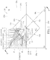
- FIG. 1 is a perspective top view of an electronic package according to one embodiment of the invention.
- FIG. 2 is a schematic, cross-sectional diagram taken alone line I-I' in FIG. 1 .
- FIG. 3 is a perspective view of the electronic package according to one embodiment of the invention.
- an electronic package 1 comprises a chip package 10 that is mounted on a top surface 201 of a package substrate 20 in a flip-chip manner and may be bonded to the top surface 201 with bumps 30.
- the chip package 10 and the package substrate 20 may both have a rectangular shape when viewed from the above.
- the chip package 10 and the package substrate 20 may both have a square shape having four sides of equal length.
- the chip package 10 has four sides 10a ⁇ 10d.
- the package substrate 20 has four vertices A ⁇ D and four sides 20a ⁇ 20d between the four vertices A ⁇ D, respectively.
- the top surface 201 of the package substrate 20 may be partitioned into four 90-degree quadrants Q 1 ⁇ Q 4 by two orthogonal axes (reference X and Y axes) in a two-dimensional plane (parallel to the top surface 201).
- the quadrants Q 1 and Q 3 are diagonally opposite each other.
- the quadrants Q 2 and Q 4 are diagonally opposite each other
- FIG. 1 to FIG. 3 a reference Z axis that is orthogonal to the top surface 201 or X-Y plane is shown.
- the package substrate 20 may be an organic substrate comprising laminated organic material or a core 200, such as epoxy or the like. As shown in FIG. 2 , a plurality of solder balls 230 may be disposed on a bottom surface 202 of the package substrate 20.
- the chip package 10 is mounted on the top surface 201 of a package substrate 20 through a plurality of solder joints or bumps 30.
- An underfill 40 may be dispensed to fill a gap (or standoff) between the chip package 10 and the package substrate 20.
- the package substrate 20 may comprise multiple layers of traces, for example, traces 211 and 221.
- the trace 211 is intended to be disposed in the topmost layer of the multiple layers of traces of the package substrate 20.
- the traces 211 may be covered with a protection layer 280 such as a solder mask or the like, but is not limited thereto.
- the bump 30 is joined to and aligned with a corresponding bump pad 210 situated, for example, at one distal end of the trace 211.
- the trace 211 extends toward the corner at the vertex A or toward the two adjacent sides 20a and 20b around the corner.
- the traces 211 for electrically connecting the corresponding bump pads 210 are generally disposed within the exemplary revealed quadrant Q 2 .
- the trace 211 is electrically coupled to a connection pad 212.
- a plated through hole (PTH) 213 may be provided to electrically connect the connection pad 212 to a solder ball pad 214 at the bottom surface 202 of the package substrate 20.
- a solder ball 230 is planted on the solder ball pad 214 for further connection with a system board or a printed circuit board (PCB).
- PCB printed circuit board
- connection pads 212 is aligned with the solder ball pads 214 and therefore the solder balls 230, the position of each connection pad 212 in FIG. 1 generally represents the position of each solder ball 230. It is understood that the configuration as indicated in quadrant Q 2 may be employed in the other quadrants Q 1 , Q 3 and Q 4 in other embodiments.
- the chip package 10 and the package substrate 20 may have the same center point CP and therefore have a concentric configuration with the chip package that is angular offset relative to the package substrate 20.
- the chip package 10 is rotated relative to the package substrate 20 about the Z axis by a rotation offset angle ⁇ of about 45 degrees, wherein the rotation offset angle ⁇ is the included angle between the reference Y axis and the direction of the side 10b or 10d of the chip package 10.
- ⁇ is the included angle between the reference Y axis and the direction of the side 10b or 10d of the chip package 10.
- none of the four sides 10a ⁇ 10d of the chip package 10 is parallel with any of the four sides 20a ⁇ 20d of the package substrate 20.
- the chip package 10 It is intended to rotate the chip package 10 such that its one side 10a directly faces one corner at vertex A of the package substrate 20.
- the two sides 20a and 20b of the package substrate 20 are joined at the vertex A.
- the two sides 20a and 20b define boundaries of the 90-degree quadrant Q 2 .
- the chip package 10 comprises a first high-speed interface circuit die 11, which may be operated at high-speed data transmission rate of at least 1000Mbps at frequency higher than 500MHz.
- the first high-speed interface circuit die 11 may be encapsulated within a molding compound 50.
- the first high-speed interface circuit die 11 comprises a first Serializer/Deserializer (SerDes) circuit block 110 that is located in close proximity to the side 10a that directly faces one corner at vertex A of the package substrate 20.
- SerDes Serializer/Deserializer
- the first high-speed interface circuit die 11 comprises a first edge 11a directly facing the corner at the vertex A of the package substrate 20, a second edge 11b that is perpendicular to the first edge 11a and is joined to the first edge 11a, and a third edge 11c that is perpendicular to the first edge 11a and is joined to the first edge 11a.
- the first edge 11a is in parallel with the side 10a of the chip package 10
- the second edge 11b is in parallel with the side 10d of the chip package
- the third edge 11c is parallel with the side 10b of the chip package 10.
- the second edge 11b and the third edge 11c are in parallel with a diagonal line DL extending between the vertex A and the vertex C.
- a first row of input/output (I/O) pads 111a is disposed along the first edge 11a
- a second row of I/O pads 111b is disposed along the second edge 11b
- a third row of I/O pads 111c is disposed along the third edge 11c. It is understood that these I/O pads 111 are disposed at a bottom of the first high-speed interface circuit die 11.
- a redistribution layer (RDL) structure 100 may be provided between the first high-speed interface circuit die 11 and the top surface 201 of the package substrate 20 to fan-out the I/O pads 111.
- the RDL structure 100 which is known in the art, may be composed of dielectric layers and interconnect structures in the dielectric layers for electrically connecting the I/O pads of the high-speed interface circuit die 11 to the corresponding bump pads 101 on which the bump 30 is formed.
- the chip package 10 may be a fan-out wafer level package (FOWLP).
- the first SerDes circuit block 110 of the first high-speed interface circuit die 11, the edges 11a ⁇ 11c, the rows of I/O pads 111a ⁇ 111c are generally disposed within the exemplary quadrant Q 2 . It is understood that the chip package 10 is flipped with its active surface mounted on the top surface 201 of the package substrate 20 in a flip-chip manner.
- a first group of solder balls P 1 solder balls are not explicitly shown in FIG. 1 , but aligned with the connection pads 212a
- the first row of I/O pads 111a disposed at the first edge 11a of the high-speed interface circuit die 11 is electrically connected to the first group of solder balls P 1 through the traces 211a, respectively, within the quadrant Q 2 on the top surface 201 of the package substrate 20.
- a second group of solder balls P 2 (solder balls are not explicitly shown in FIG. 1 , but aligned with the connection pads 212b) is arranged along the side 20a adjacent to the corner at the vertex A.
- the second row of I/O pads 111b is electrically connected to the second group of solder balls P 2 through traces 211b, respectively, within the quadrant Q 2 on the top surface 201 of the package substrate 20.
- a third group of solder balls P 3 (solder balls are not explicitly shown in FIG. 1 , but aligned with the connection pads 212c) is arranged along the side 20b adjacent to the corner at the vertex A.
- the third row of I/O pads 111c is electrically connected to the third group of solder balls P 3 through traces 211c, respectively, within the quadrant Q 2 on the top surface 201 of the package substrate 20.
- the chip package 10 may further comprises a second high-speed interface circuit die 12 in proximity to the first high-speed interface circuit die 11.
- the second high-speed interface circuit die 12 may comprise a SerDes circuit block 120 and may have similar trace and ball arrangement in the quadrant Q 4 of the top surface 201 of the package substrate 20.
- the first high-speed interface circuit die 11 may be electrically connected to the second high-speed interface circuit die 12 through the RDL structure 100.
- the I/O pad 111d of the first high-speed interface circuit die 11 is electrically connected to the I/O pad 121d of the second high-speed interface circuit die 12 through the interconnect line 103 in the RDL structure 100.
- the present disclosure because by providing the rotated chip package configuration, the corresponding traces and ball arrangement on the package substrate are concentrated within one of the four quadrants Q 1 ⁇ Q 4 , resulting in a 14.3% reduction of the maximum signal length (e.g., from about 35mm to about30mm for 60x60mm ⁇ 90x90mm package substrate), and a significant reduction of trace length difference (max. length minus min. length) from 20mm to 13mm. Therefore, the skew is mitigated and the signal delay as well as the electrical performance of SerDes circuit of the electronic package can be significantly improved (e.g., with improvement by 18% or about -0.5dB).
- rotation offset angle ⁇ of approximately 45 degrees is used in the illustrative embodiment(s)
- the rotated die design in the electronic package 1 is not limited to this angle in other embodiments.
- the rotation offset angle ⁇ may range between 30 and 75 degrees in some embodiments.
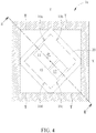
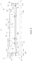
- FIG. 4 and FIG. 5 show an electronic package with metal ring and rotated semiconductor die on the package substrate, wherein like layers, elements, or regions are designated by like numeral numbers and labels.
- the electronic package 1a according to the invention may comprise a metal ring (or metal frame) 60 that is adhered to the top surface 201 of the package substrate 20 with an adhesive layer 610.
- the metal ring 60 may be a copper ring, but is not limited thereto.
- the package substrate 20 has a rectangular shape and has four corners.
- the chip package 10 comprises a first high-speed interface circuit die 11 mounted on the top surface 201 of the package substrate 20, and a second high-speed interface circuit die 12 disposed in proximity to the first high-speed interface circuit die 11.
- the chip package 10, the first high-speed interface circuit die 11, and the second high-speed interface circuit die 12 are rotated relative to the package substrate 20 about a vertical axis (Z axis in FIG. 5 ) that is orthogonal to the top surface 201 by a rotation offset angle ⁇ .
- the rotated chip package 10 on the package substrate 20 can provide some space in the triangular regions T at each of the four corners of the electronic package 1a for the improvements on warpage control or electrical performance.
- the metal ring 60 may be replaced with a metal lid 60a that covers the top surface of the chip package 10 in some embodiments, as shown in FIG. 6 .
- the molding compound 50 of the electronic package 1b may be polished until the top surfaces of the first high-speed interface circuit die 11 and the second high-speed interface circuit die 12 are exposed.
- the metal lid 60a may be in thermal contact with the exposed top surfaces of the first high-speed interface circuit die 11 and the second high-speed interface circuit die 12.
- the triangular regions T between the metal ring 60 and the chip package 10 may be used to accommodate more decoupling capacitors 70 in the triangular regions T at each of the four corners. Therefore, the electronic package 1c comprises more decoupling capacitors at the corners of the package, thereby improving the electrical performance such as the performance of the power distribution network (PDN).
- PDN power distribution network
- At least one decoupling capacitor 70 may be disposed at the corner of the package substrate 20 wherein the decoupling capacitor 70 is rotated relative to the package substrate 20 about a vertical axis (Z axis in FIG. 5 ) that is orthogonal to the top surface 201 by a rotation offset angle ⁇ .
- the triangular regions T between the metal ring 60 and the chip package 10 may be used to accommodate more chips 80 or chips with a larger size.
- the chips 80 disposed within the triangular regions T may be rotated or non-rotated.
- the multi-chip modules could be larger and more symmetric, resulting in better package warpage control and improved electrical performance.
- the modules could be molding-type (with or without function) packages to balance the coefficient of thermal expansion (CTE) mismatch and improve the package warpage.
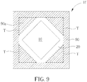
- the metal ring 90 may comprise an extension portion 90a within the triangular regions T between the metal ring 60 and the chip package 10 as indicated by dotted line in FIG. 4 .
- the package warpage control is improved because of the wider ring foot standing at the four corners of the electronic package If.
Landscapes
- Semiconductor Integrated Circuits (AREA)
- Physics & Mathematics (AREA)
- Geometry (AREA)
- Wire Bonding (AREA)
- Structures For Mounting Electric Components On Printed Circuit Boards (AREA)
Abstract
Description
- This application claims benefits from
U.S. provisional application No. 62/848,064 filed May 15, 2019 - The present disclosure relates generally to the field of semiconductor packaging. More particularly, the present disclosure relates to an electronic package with a rotated semiconductor die.
- Typically, a data communication network includes multiple communication devices and a connection infrastructure or medium for interconnecting or networking the communication devices. The communication devices may include embedded controllers. The communication devices may connect with high-speed analog serial data interfaces or ports configured to operate at Gigabit-per-second (Gbps) data rates (e.g., 56Gbps or 112 Gbps). The serial data interfaces are configured in accordance with known data transmission standards. The connection infrastructure is capable of interfacing with such high-speed analog serial data interfaces.
- The use of high-speed serial communication links in electronic systems has continued to grow. As known in the art, high-speed data links transmit data from one location to another over transmission lines. These data links can include Serializer/Deserializer data links (i.e. SerDes) that receive data in a parallel format and convert the data to a serial format for high speed transmission. SerDes data links can be part of a backplane in a communications system.
- However, the prior art chip packages for high-data communication applications, which contain SerDes circuits, usually suffer from so-called SerDes loss arose from signal skew or signal delay, which in turn deteriorates the electrical performance of the chip package.
- Further, it is difficult to control the coplanarity and warpage of the conventional large-size chip packages. Typically, to improve the warpage for the large-size chip packages, the foot width of the metal lid or ring is increased or dummy dies are added at open areas. Conventionally, the orientation of the fan-out die attachment is 0, 90, or 270, which is limited by substrate trace design, substrate marks such as bar code, fiducial mark or the like, and ring/lid foot width design at substrate corners.
- It is one object of the present disclosure to provide an improved semiconductor electronic package for high-data rate communication applications, which is capable of reducing signal skew or signal delay and thus improving electrical performance of the semiconductor electronic package.
- It is another object of the present disclosure to provide an improved semiconductor electronic package with metal ring and rotated semiconductor die, which is capable of improving warpage control of the package.
- An electronic package according to the invention is defined in
independent claim 1. The dependent claims define preferred embodiments thereof. - One aspect of the present disclosure provides an electronic package includes a package substrate of a rectangular shape; a chip package comprising a first high-speed interface circuit die, mounted on a top surface of the package substrate, wherein the chip package and/or the first high-speed interface circuit die is rotated relative to the package substrate about a vertical axis that is orthogonal to the top surface by a rotation offset angle; and a metal ring mounted on the top surface of the package substrate.
- Preferably, the rotation offset angle is between 30 and 75 degrees.
- Preferably, the rotation offset angle is about 45 degrees, in particular 45 degrees.
- Preferably, the top surface of the package substrate is partitioned into four quadrants by two orthogonal axes in a two-dimensional plane.
- Preferably, the first high-speed interface circuit die comprises a first edge directly facing a vertex of the package substrate, wherein a first row of input/output (I/O) pads is disposed along the first edge.
- Preferably, the first high-speed interface circuit die comprises a second edge that is perpendicular to the first edge, wherein a second row of input/output (I/O) pads is disposed along the second edge.
- Preferably, a first group of solder balls is arranged along two sides joined at said vertex of the package substrate, and wherein said first row of I/O pads is electrically connected to the first group of solder balls through a plurality first traces, respectively, within one of the four quadrants on the top surface of the package substrate.
- Preferably, a second group of solder balls is arranged along one of said two sides joined at said vertex of the package substrate, and wherein said second row of I/O pads is electrically connected to the second group of solder balls through a plurality second traces, respectively, within said one of the four quadrants on the top surface of the package substrate.
- Preferably, the first high-speed interface circuit die comprises a first Serializer/Deserializer (SerDes) circuit block.
- Preferably, the electronic package further includes a second high-speed interface circuit die in proximity to the first high-speed interface circuit die.
- Preferably, the second high-speed interface circuit die comprises a second Serializer/Deserializer (SerDes) circuit block.
- Preferably, the first high-speed interface circuit die is electrically connected to the second high-speed interface circuit die through a redistribution layer (RDL) structure.
- Preferably, the electronic package further includes a plurality of capacitors disposed within a triangular region between the metal ring and a side of the rotated chip package.
- Preferably, the electronic package further includes a plurality of chips disposed within a triangular region between the metal ring and a side of the rotated chip package.
- Preferably, the plurality of chips is rotated or non-rotated.
- Preferably, the metal ring comprises an extension portion disposed within a triangular region between the metal ring and a side of the rotated chip package for warpage control.
- Preferably, the electronic package further includes at least one decoupling capacitor at a corner of the package substrate, wherein the decoupling capacitor is rotated relative to the package substrate about a vertical axis that is orthogonal to the top surface by a rotation offset angle.
- These and other objectives of the present invention will no doubt become obvious to those of ordinary skill in the art after reading the following detailed description of the preferred embodiment that is illustrated in the various figures and drawings.
- The accompanying drawings are included to provide a further understanding of the invention, and are incorporated in and constitute a part of this specification. The drawings illustrate embodiments of the invention and, together with the description, serve to explain the principles of the invention. In the drawings:
-
FIG. 1 is a perspective top view of a semiconductor electronic package according to one embodiment of the invention; -
FIG. 2 is a schematic, cross-sectional diagram taken alone line I-I' inFIG. 1 ; -
FIG. 3 is a perspective view of the semiconductor electronic package according to one embodiment of the invention; -
FIG. 4 is a schematic top view of an electronic package with metal ring and rotated semiconductor die on the package substrate; -
FIG. 5 is schematic, cross-sectional view taken alone line II-II' inFIG. 4 ; -
FIG. 6 is schematic, cross-sectional diagram showing an electronic package with metal lid according to another embodiment of the invention; -
FIG. 7 is a schematic top view of an electronic package with metal ring and rotated semiconductor die showing that more decoupling capacitors are disposed within the triangular regions between the metal ring and the chip package according to another embodiment of the invention; -
FIG. 8 is a schematic top view of an electronic package with metal ring and rotated semiconductor die showing that some chips are disposed within the triangular regions between the metal ring and the chip package according to another embodiment of the invention; and -
FIG. 9 is a schematic top view of an electronic package with extended metal ring for warpage control according to another embodiment of the invention. - In the following detailed description of embodiments of the invention, reference is made to the accompanying drawings, which form a part hereof, and in which is shown by way of illustration specific preferred embodiments in which the disclosure may be practiced.
- These embodiments are described in sufficient detail to enable those skilled in the art to practice them, and it is to be understood that other embodiments may be utilized and that mechanical, structural, and procedural changes may be made without departing from the spirit and scope of the present disclosure. The following detailed description is, therefore, not to be taken in a limiting sense, and the scope of embodiments of the present invention is defined only by the appended claims.
- It will be understood that, although the terms first, second, third, primary, secondary, etc. may be used herein to describe various elements, components, regions, layers and/or sections, these elements, components, regions, layers and/or sections should not be limited by these terms. These terms are only used to distinguish one element, component, region, layer or section from another region, layer or section. Thus, a first or primary element, component, region, layer or section discussed below could be termed a second or secondary element, component, region, layer or section without departing from the teachings of the present inventive concept.
- Spatially relative terms, such as "beneath", "below", "lower", "under", "above," "upper," "over" and the like, may be used herein for ease of description to describe one element or feature's relationship to another element(s) or feature(s) as illustrated in the figures. It will be understood that the spatially relative terms are intended to encompass different orientations of the device in use or operation in addition to the orientation depicted in the figures. For example, if the device in the figures is turned over, elements described as "below" or "beneath" or "under" other elements or features would then be oriented "above" or "over" the other elements or features. Thus, the exemplary terms "below" and "under" can encompass both an orientation of above and below. The device may be otherwise oriented (rotated 90 degrees or at other orientations) and the spatially relative descriptors used herein interpreted accordingly. In addition, it will also be understood that when a layer is referred to as being "between" two layers, it can be the only layer between the two layers, or one or more intervening layers may also be present.
- The terminology used herein is for the purpose of describing particular embodiments only and is not intended to be limiting of the inventive concept. As used herein, the singular forms "a", "an" and "the" are intended to include the plural forms as well, unless the context clearly indicates otherwise. It will be further understood that the terms "comprises" and/or "comprising," when used in this specification, specify the presence of stated features, integers, steps, operations, elements, and/or components, but do not preclude the presence or addition of one or more other features, integers, steps, operations, elements, components, and/or groups thereof. As used herein, the term "and/or" includes any and all combinations of one or more of the associated listed items, and may be abbreviated as "/".
- It will be understood that when an element or layer is referred to as being "on", "connected to", "coupled to", or "adjacent to" another element or layer, it can be directly on, connected, coupled, or adjacent to the other element or layer, or intervening elements or layers may be present. In contrast, when an element is referred to as being "directly on," "directly connected to", "directly coupled to", or "immediately adjacent to" another element or layer, there are no intervening elements or layers present.
- A Serializer/Deserializer (SerDes) is a pair of functional blocks commonly used in high-speed communications to compensate for limited input/output. These blocks convert data between serial data and parallel interfaces in each direction. The term "SerDes" generically refers to interfaces used in various technologies and applications. The primary use of a SerDes is to provide data transmission over a single line or a differential pair in order to minimize the number of I/O pins and interconnects. SerDes data transmission implementations can be used in a wide range of communication systems and devices, such as mobile devices, desktop computers and servers, computer networks, and telecommunication networks.
- The disclosed electronic package, which is configured to operate at Gigabit-per-second (Gbps) data rates, is capable of reducing signal skew and thus improving electrical performance of the chip package, which is suited for high-data rate communication applications including, but not limited to, hyper scale data centers, ultra-high performance networking switches, routers or compute applications as well as 4G and 5G service provider (backhaul) infrastructure, AI/Deep-learning applications, and novel computing applications.
- Please refer to
FIG. 1 to FIG. 3 .FIG. 1 is a perspective top view of an electronic package according to one embodiment of the invention.FIG. 2 is a schematic, cross-sectional diagram taken alone line I-I' inFIG. 1 .FIG. 3 is a perspective view of the electronic package according to one embodiment of the invention. - As shown in
FIG. 1 to FIG. 3 , in accordance with one embodiment, anelectronic package 1 comprises achip package 10 that is mounted on atop surface 201 of apackage substrate 20 in a flip-chip manner and may be bonded to thetop surface 201 withbumps 30. Thechip package 10 and thepackage substrate 20 may both have a rectangular shape when viewed from the above. For example, thechip package 10 and thepackage substrate 20 may both have a square shape having four sides of equal length. Thechip package 10 has foursides 10a∼10d. Thepackage substrate 20 has four vertices A∼D and foursides 20a∼20d between the four vertices A∼D, respectively. - As shown in
FIG. 1 , thetop surface 201 of thepackage substrate 20 may be partitioned into four 90-degree quadrants Q1∼Q4 by two orthogonal axes (reference X and Y axes) in a two-dimensional plane (parallel to the top surface 201). The quadrants Q1 and Q3 are diagonally opposite each other. The quadrants Q2 and Q4 are diagonally opposite each other ThroughFIG. 1 to FIG. 3 , a reference Z axis that is orthogonal to thetop surface 201 or X-Y plane is shown. - Preferably, the
package substrate 20 may be an organic substrate comprising laminated organic material or acore 200, such as epoxy or the like. As shown inFIG. 2 , a plurality ofsolder balls 230 may be disposed on abottom surface 202 of thepackage substrate 20. Thechip package 10 is mounted on thetop surface 201 of apackage substrate 20 through a plurality of solder joints or bumps 30. Anunderfill 40 may be dispensed to fill a gap (or standoff) between thechip package 10 and thepackage substrate 20. Thepackage substrate 20 may comprise multiple layers of traces, for example, traces 211 and 221. - In
FIG. 2 , thetrace 211 is intended to be disposed in the topmost layer of the multiple layers of traces of thepackage substrate 20. Typically, thetraces 211 may be covered with aprotection layer 280 such as a solder mask or the like, but is not limited thereto. Thebump 30 is joined to and aligned with acorresponding bump pad 210 situated, for example, at one distal end of thetrace 211. Thetrace 211 extends toward the corner at the vertex A or toward the twoadjacent sides - The
traces 211 for electrically connecting thecorresponding bump pads 210 are generally disposed within the exemplary revealed quadrant Q2. Thetrace 211 is electrically coupled to aconnection pad 212. A plated through hole (PTH) 213 may be provided to electrically connect theconnection pad 212 to asolder ball pad 214 at thebottom surface 202 of thepackage substrate 20. Asolder ball 230 is planted on thesolder ball pad 214 for further connection with a system board or a printed circuit board (PCB). - For the sake of simplicity, only the traces and ball arrangement within the quadrant Q2 is revealed in perspective view as shown in
FIG. 1 . Thesolder balls 230 are not expressly shown inFIG. 1 . However, it is understood that since theconnection pads 212 is aligned with thesolder ball pads 214 and therefore thesolder balls 230, the position of eachconnection pad 212 inFIG. 1 generally represents the position of eachsolder ball 230. It is understood that the configuration as indicated in quadrant Q2 may be employed in the other quadrants Q1, Q3 and Q4 in other embodiments. - As shown in
FIG. 1 andFIG. 3 , thechip package 10 and thepackage substrate 20 may have the same center point CP and therefore have a concentric configuration with the chip package that is angular offset relative to thepackage substrate 20. Preferably, for example, thechip package 10 is rotated relative to thepackage substrate 20 about the Z axis by a rotation offset angle θ of about 45 degrees, wherein the rotation offset angle θ is the included angle between the reference Y axis and the direction of theside chip package 10. Preferably, none of the foursides 10a∼10d of thechip package 10 is parallel with any of the foursides 20a∼20d of thepackage substrate 20. - It is intended to rotate the
chip package 10 such that its oneside 10a directly faces one corner at vertex A of thepackage substrate 20. The twosides package substrate 20 are joined at the vertex A. The twosides - Preferably, the
chip package 10 comprises a first high-speed interface circuit die 11, which may be operated at high-speed data transmission rate of at least 1000Mbps at frequency higher than 500MHz. As shown inFIG. 2 , the first high-speed interface circuit die 11 may be encapsulated within amolding compound 50. Preferably, the first high-speed interface circuit die 11 comprises a first Serializer/Deserializer (SerDes)circuit block 110 that is located in close proximity to theside 10a that directly faces one corner at vertex A of thepackage substrate 20. - Preferably, as shown in
FIG. 1 , the first high-speed interface circuit die 11 comprises afirst edge 11a directly facing the corner at the vertex A of thepackage substrate 20, asecond edge 11b that is perpendicular to thefirst edge 11a and is joined to thefirst edge 11a, and athird edge 11c that is perpendicular to thefirst edge 11a and is joined to thefirst edge 11a. Preferably, thefirst edge 11a is in parallel with theside 10a of thechip package 10, thesecond edge 11b is in parallel with theside 10d of thechip package 10, and thethird edge 11c is parallel with theside 10b of thechip package 10. Thesecond edge 11b and thethird edge 11c are in parallel with a diagonal line DL extending between the vertex A and the vertex C. - Preferably, as shown in
FIG. 1 , a first row of input/output (I/O)pads 111a is disposed along thefirst edge 11a, a second row of I/O pads 111b is disposed along thesecond edge 11b, and a third row of I/O pads 111c is disposed along thethird edge 11c. It is understood that these I/O pads 111 are disposed at a bottom of the first high-speed interface circuit die 11. - Preferably, a redistribution layer (RDL)
structure 100 may be provided between the first high-speed interface circuit die 11 and thetop surface 201 of thepackage substrate 20 to fan-out the I/O pads 111. TheRDL structure 100, which is known in the art, may be composed of dielectric layers and interconnect structures in the dielectric layers for electrically connecting the I/O pads of the high-speed interface circuit die 11 to thecorresponding bump pads 101 on which thebump 30 is formed. Preferably, thechip package 10 may be a fan-out wafer level package (FOWLP). - Preferably, the first
SerDes circuit block 110 of the first high-speed interface circuit die 11, theedges 11a∼11c, the rows of I/O pads 111a∼111c are generally disposed within the exemplary quadrant Q2. It is understood that thechip package 10 is flipped with its active surface mounted on thetop surface 201 of thepackage substrate 20 in a flip-chip manner. - As shown in
FIG. 1 , preferably, a first group of solder balls P1 (solder balls are not explicitly shown inFIG. 1 , but aligned with theconnection pads 212a) is arranged along twosides package substrate 20. The first row of I/O pads 111a disposed at thefirst edge 11a of the high-speed interface circuit die 11 is electrically connected to the first group of solder balls P1 through thetraces 211a, respectively, within the quadrant Q2 on thetop surface 201 of thepackage substrate 20. - Preferably, a second group of solder balls P2 (solder balls are not explicitly shown in
FIG. 1 , but aligned with theconnection pads 212b) is arranged along theside 20a adjacent to the corner at the vertex A. The second row of I/O pads 111b is electrically connected to the second group of solder balls P2 throughtraces 211b, respectively, within the quadrant Q2 on thetop surface 201 of thepackage substrate 20. - Preferably, a third group of solder balls P3 (solder balls are not explicitly shown in
FIG. 1 , but aligned with theconnection pads 212c) is arranged along theside 20b adjacent to the corner at the vertex A. The third row of I/O pads 111c is electrically connected to the third group of solder balls P3 throughtraces 211c, respectively, within the quadrant Q2 on thetop surface 201 of thepackage substrate 20. - Preferably, as shown in
FIG. 2 , thechip package 10 may further comprises a second high-speed interface circuit die 12 in proximity to the first high-speed interface circuit die 11. The second high-speed interface circuit die 12 may comprise aSerDes circuit block 120 and may have similar trace and ball arrangement in the quadrant Q4 of thetop surface 201 of thepackage substrate 20. The first high-speed interface circuit die 11 may be electrically connected to the second high-speed interface circuit die 12 through theRDL structure 100. For example, the I/O pad 111d of the first high-speed interface circuit die 11 is electrically connected to the I/O pad 121d of the second high-speed interface circuit die 12 through theinterconnect line 103 in theRDL structure 100. - It is advantageous to use the present disclosure because by providing the rotated chip package configuration, the corresponding traces and ball arrangement on the package substrate are concentrated within one of the four quadrants Q1∼Q4, resulting in a 14.3% reduction of the maximum signal length (e.g., from about 35mm to about30mm for 60x60mm∼90x90mm package substrate), and a significant reduction of trace length difference (max. length minus min. length) from 20mm to 13mm. Therefore, the skew is mitigated and the signal delay as well as the electrical performance of SerDes circuit of the electronic package can be significantly improved (e.g., with improvement by 18% or about -0.5dB).
- It is noteworthy that although a rotation offset angle θ of approximately 45 degrees is used in the illustrative embodiment(s), the rotated die design in the
electronic package 1 is not limited to this angle in other embodiments. For example, the rotation offset angle θ may range between 30 and 75 degrees in some embodiments. -
FIG. 4 andFIG. 5 show an electronic package with metal ring and rotated semiconductor die on the package substrate, wherein like layers, elements, or regions are designated by like numeral numbers and labels. As shown inFIG. 4 andFIG. 5 , the electronic package 1a according to the invention may comprise a metal ring (or metal frame) 60 that is adhered to thetop surface 201 of thepackage substrate 20 with anadhesive layer 610. Preferably, themetal ring 60 may be a copper ring, but is not limited thereto. Preferably, thepackage substrate 20 has a rectangular shape and has four corners. - As previously described, the
chip package 10 comprises a first high-speed interface circuit die 11 mounted on thetop surface 201 of thepackage substrate 20, and a second high-speed interface circuit die 12 disposed in proximity to the first high-speed interface circuit die 11. Thechip package 10, the first high-speed interface circuit die 11, and the second high-speed interface circuit die 12 are rotated relative to thepackage substrate 20 about a vertical axis (Z axis inFIG. 5 ) that is orthogonal to thetop surface 201 by a rotation offset angle θ. - As indicated by dotted line in
FIG. 4 , the rotatedchip package 10 on thepackage substrate 20 can provide some space in the triangular regions T at each of the four corners of the electronic package 1a for the improvements on warpage control or electrical performance. - It is to be understood that the
metal ring 60 may be replaced with ametal lid 60a that covers the top surface of thechip package 10 in some embodiments, as shown inFIG. 6 . InFIG. 6 , themolding compound 50 of the electronic package 1b may be polished until the top surfaces of the first high-speed interface circuit die 11 and the second high-speed interface circuit die 12 are exposed. Themetal lid 60a may be in thermal contact with the exposed top surfaces of the first high-speed interface circuit die 11 and the second high-speed interface circuit die 12. - Preferably, as shown in
FIG. 7 , the triangular regions T between themetal ring 60 and thechip package 10 may be used to accommodatemore decoupling capacitors 70 in the triangular regions T at each of the four corners. Therefore, the electronic package 1c comprises more decoupling capacitors at the corners of the package, thereby improving the electrical performance such as the performance of the power distribution network (PDN). - Preferably, at least one
decoupling capacitor 70 may be disposed at the corner of thepackage substrate 20 wherein thedecoupling capacitor 70 is rotated relative to thepackage substrate 20 about a vertical axis (Z axis inFIG. 5 ) that is orthogonal to thetop surface 201 by a rotation offset angle θ. - Preferably, as shown in
FIG. 8 , the triangular regions T between themetal ring 60 and thechip package 10 may be used to accommodatemore chips 80 or chips with a larger size. Thechips 80 disposed within the triangular regions T may be rotated or non-rotated. By providing such configuration in the electronic package Id, the multi-chip modules could be larger and more symmetric, resulting in better package warpage control and improved electrical performance. The modules could be molding-type (with or without function) packages to balance the coefficient of thermal expansion (CTE) mismatch and improve the package warpage. - Preferably, as shown in
FIG. 9 , themetal ring 90 may comprise anextension portion 90a within the triangular regions T between themetal ring 60 and thechip package 10 as indicated by dotted line inFIG. 4 . The package warpage control is improved because of the wider ring foot standing at the four corners of the electronic package If. - Those skilled in the art will readily observe that numerous modifications and alterations of the device and method may be made while retaining the teachings of the invention. Accordingly, the above disclosure should be construed as limited only by the metes and bounds of the appended claims.
Claims (15)
- An electronic package (1; 1a; 1b; 1c), comprising:a package substrate (20) of a rectangular shape;a chip package (10) comprising a first high-speed interface circuit die (11), mounted on a top surface (201) of the package substrate (20), wherein the chip package (10) and/or the first high-speed interface circuit die (11) is rotated relative to the package substrate (20) about a vertical axis (Z) that is orthogonal to the top surface (201) by a rotation offset angle (θ); anda metal ring (60; 90) mounted on the top surface (201) of the package substrate (20).
- The electronic package according to claim 1, wherein the rotation offset angle is between 30 and 75 degrees.
- The electronic package according to claim 1 or 2, wherein the rotation offset angle is about 45 degrees.
- The electronic package according to any one of claims 1 to 3, wherein the top surface (201) of the package substrate (20) is partitioned into four quadrants (Q1 - Q4) by two orthogonal axes (X, Y) in a two-dimensional plane.
- The electronic package according to claim 4, wherein the first high-speed interface circuit die (11) comprises a first edge (11a) directly facing a vertex (A) of the package substrate (20), wherein a first row of input/output, in the following also referred to as I/O, pads (111a) is disposed along the first edge (11a).
- The electronic package according to claim 5, wherein the first high-speed interface circuit die (11) comprises a second edge (11b) that is perpendicular to the first edge (11a), wherein a second row of I/O pads (111b) is disposed along the second edge (11b).
- The electronic package according to claim 5 or 6, wherein a first group of solder balls (P1) is arranged along two sides (20a, 20b) joined at said vertex (A) of the package substrate (20), and wherein said first row of I/O pads (111a) is electrically connected to the first group of solder balls (P1) through a plurality first traces (211a), respectively, within one of the four quadrants (Q2) on the top surface (201) of the package substrate (20).
- The electronic package according to claim 7, wherein a second group of solder balls (P2) is arranged along one of said two sides (20a) joined at said vertex (A) of the package substrate (20), and wherein said second row of I/O pads (111b) is electrically connected to the second group of solder balls (P2) through a plurality second traces (211b), respectively, within said one of the four quadrants (Q2) on the top surface (201) of the package substrate (20).
- The electronic package according to any one of claims 1 to 8, wherein the first high-speed interface circuit die (11) comprises a first Serializer/Deserializer, in the following also referred to as SerDes, circuit block.
- The electronic package according to any one of claims 1 to 9, further comprising:
a second high-speed interface circuit die (12) in proximity to the first high-speed interface circuit die (11). - The electronic package according to claim 10, wherein the second high-speed interface circuit die (12) comprises a second SerDes circuit block.
- The electronic package according to claim 10 or 11, wherein the first high-speed interface circuit die (11) is electrically connected to the second high-speed interface circuit die (12) through a redistribution layer, in the following also referred to as RDL, structure (100).
- The electronic package according to any one of claims 1 to 12, further comprising:a plurality of capacitors (70) disposed within a triangular region (T) between the metal ring (60; 90) and a side of the rotated chip package; and/ora plurality of chips (80) disposed within a triangular region (T) between the metal ring (60 90) and a side of the rotated chip package, wherein preferably the plurality of chips (80) is rotated or non-rotated.
- The electronic package according to any one of claims 1 to 13, wherein the metal ring (90) comprises an extension portion (90a) disposed within a triangular region (T) between the metal ring (90) and a side of the rotated chip package for warpage control.
- The electronic package according to any one of claims 1 to 12, further comprising:
at least one decoupling capacitor (70) at a corner of the package substrate (20), wherein the decoupling capacitor (70) is rotated relative to the package substrate (20) about a vertical axis (Z) that is orthogonal to the top surface (201) by a rotation offset angle (θ).
Applications Claiming Priority (2)
| Application Number | Priority Date | Filing Date | Title |
|---|---|---|---|
| US201962848064P | 2019-05-15 | 2019-05-15 | |
| US16/846,381 US11222850B2 (en) | 2019-05-15 | 2020-04-12 | Electronic package with rotated semiconductor die |
Publications (2)
| Publication Number | Publication Date |
|---|---|
| EP3739626A1 true EP3739626A1 (en) | 2020-11-18 |
| EP3739626B1 EP3739626B1 (en) | 2025-10-22 |
Family
ID=70483040
Family Applications (1)
| Application Number | Title | Priority Date | Filing Date |
|---|---|---|---|
| EP20172494.5A Active EP3739626B1 (en) | 2019-05-15 | 2020-04-30 | Electronic package with rotated semiconductor die |
Country Status (4)
| Country | Link |
|---|---|
| US (3) | US11222850B2 (en) |
| EP (1) | EP3739626B1 (en) |
| CN (2) | CN115985861A (en) |
| TW (1) | TWI719897B (en) |
Families Citing this family (8)
| Publication number | Priority date | Publication date | Assignee | Title |
|---|---|---|---|---|
| US11222850B2 (en) * | 2019-05-15 | 2022-01-11 | Mediatek Inc. | Electronic package with rotated semiconductor die |
| TWI735398B (en) * | 2020-12-21 | 2021-08-01 | 矽品精密工業股份有限公司 | Electronic package and manufacturing method thereof |
| US11562962B2 (en) * | 2021-01-13 | 2023-01-24 | Qualcomm Incorporated | Package comprising a substrate and interconnect device configured for diagonal routing |
| TWI819441B (en) * | 2021-05-05 | 2023-10-21 | 威盛電子股份有限公司 | Package substrate, chip package and integrated circuit chip |
| CN114496971A (en) * | 2021-05-05 | 2022-05-13 | 威盛电子股份有限公司 | Packaging substrate, chip packaging body and integrated circuit chip |
| DE102021120398B4 (en) * | 2021-08-05 | 2023-03-02 | Infineon Technologies Ag | SYSTEMS AND DEVICES FOR WHEEL SENSORS |
| CN114927491A (en) * | 2022-05-17 | 2022-08-19 | 超聚变数字技术有限公司 | Electronic device, circuit board and chip |
| US20230395524A1 (en) * | 2022-06-06 | 2023-12-07 | Intel Corporation | Emi cage for microstrip routing via dual layer underfill concept |
Citations (8)
| Publication number | Priority date | Publication date | Assignee | Title |
|---|---|---|---|---|
| US20020145197A1 (en) * | 2001-03-23 | 2002-10-10 | Ngk Spark Plug Co., Ltd. | Wiring substrate |
| US20080179735A1 (en) * | 2007-01-30 | 2008-07-31 | Kabushiki Kaisha Toshiba | System in package device |
| US20100155927A1 (en) * | 2008-12-23 | 2010-06-24 | Kee Leong Cheah | Semiconductor packages with stiffening support for power delivery |
| US20120127774A1 (en) * | 2009-08-07 | 2012-05-24 | Panasonic Corporation | Semiconductor device and electronic device |
| DE102013103138A1 (en) * | 2012-03-27 | 2013-10-02 | Intel Mobile Communications GmbH | Fan-out type wafer-level twisted-semiconductor device packages and method of manufacturing fan-out type wafer-level twisted semiconductor packages |
| US20140048951A1 (en) * | 2012-08-14 | 2014-02-20 | Bridge Semiconductor Corporation | Semiconductor assembly with dual connecting channels between interposer and coreless substrate |
| US20180261554A1 (en) * | 2017-03-09 | 2018-09-13 | Taiwan Semiconductor Manufacturing Company Ltd. | Semiconductor device |
| EP3582260A2 (en) * | 2018-05-18 | 2019-12-18 | MediaTek Inc. | Electronic package for high-data rate communication applications |
Family Cites Families (18)
| Publication number | Priority date | Publication date | Assignee | Title |
|---|---|---|---|---|
| US4705917A (en) * | 1985-08-27 | 1987-11-10 | Hughes Aircraft Company | Microelectronic package |
| JP2003007971A (en) * | 2001-06-25 | 2003-01-10 | Toshiba Corp | Semiconductor device |
| DE10202878A1 (en) * | 2002-01-25 | 2003-08-07 | Infineon Technologies Ag | Circuit board with integrated circuit for high speed data processing |
| TW571407B (en) * | 2002-10-25 | 2004-01-11 | Advanced Semiconductor Eng | Construction of a package with multiple modules |
| JP2008218669A (en) * | 2007-03-02 | 2008-09-18 | Nec Electronics Corp | Semiconductor device |
| WO2008149508A1 (en) * | 2007-05-31 | 2008-12-11 | Sanyo Electric Co., Ltd. | Semiconductor module and portable devices |
| TWI335055B (en) * | 2007-06-29 | 2010-12-21 | Chipmos Technologies Inc | Chip-stacked package structure |
| JP5548342B2 (en) * | 2007-10-23 | 2014-07-16 | パナソニック株式会社 | Semiconductor device |
| JP2009283835A (en) * | 2008-05-26 | 2009-12-03 | Elpida Memory Inc | Semiconductor device and method of manufacturing the same |
| US9147667B2 (en) * | 2013-10-25 | 2015-09-29 | Bridge Semiconductor Corporation | Semiconductor device with face-to-face chips on interposer and method of manufacturing the same |
| US9281296B2 (en) * | 2014-07-31 | 2016-03-08 | Invensas Corporation | Die stacking techniques in BGA memory package for small footprint CPU and memory motherboard design |
| US10242957B2 (en) * | 2015-02-27 | 2019-03-26 | Qualcomm Incorporated | Compartment shielding in flip-chip (FC) module |
| US9761571B2 (en) * | 2015-09-17 | 2017-09-12 | Deca Technologies Inc. | Thermally enhanced fully molded fan-out module |
| JP6450864B2 (en) * | 2016-02-10 | 2019-01-09 | ルネサスエレクトロニクス株式会社 | Semiconductor device |
| US9899305B1 (en) | 2017-04-28 | 2018-02-20 | Taiwan Semiconductor Manufacturing Company Ltd. | Semiconductor package structure |
| KR102439761B1 (en) * | 2017-12-22 | 2022-09-02 | 삼성전자주식회사 | Electronic devices and methods of manufacturing electronic devices |
| US12588560B2 (en) * | 2018-12-07 | 2026-03-24 | Amkor Technology Singapore Holding Pte, Ltd. | Semiconductor package and fabricating method thereof |
| US11222850B2 (en) * | 2019-05-15 | 2022-01-11 | Mediatek Inc. | Electronic package with rotated semiconductor die |
-
2020
- 2020-04-12 US US16/846,381 patent/US11222850B2/en active Active
- 2020-04-24 CN CN202310021282.2A patent/CN115985861A/en active Pending
- 2020-04-24 CN CN202010332486.4A patent/CN111952256B/en active Active
- 2020-04-30 EP EP20172494.5A patent/EP3739626B1/en active Active
- 2020-05-12 TW TW109115743A patent/TWI719897B/en active
-
2021
- 2021-12-16 US US17/553,760 patent/US11830820B2/en active Active
-
2023
- 2023-10-24 US US18/383,466 patent/US12388026B2/en active Active
Patent Citations (8)
| Publication number | Priority date | Publication date | Assignee | Title |
|---|---|---|---|---|
| US20020145197A1 (en) * | 2001-03-23 | 2002-10-10 | Ngk Spark Plug Co., Ltd. | Wiring substrate |
| US20080179735A1 (en) * | 2007-01-30 | 2008-07-31 | Kabushiki Kaisha Toshiba | System in package device |
| US20100155927A1 (en) * | 2008-12-23 | 2010-06-24 | Kee Leong Cheah | Semiconductor packages with stiffening support for power delivery |
| US20120127774A1 (en) * | 2009-08-07 | 2012-05-24 | Panasonic Corporation | Semiconductor device and electronic device |
| DE102013103138A1 (en) * | 2012-03-27 | 2013-10-02 | Intel Mobile Communications GmbH | Fan-out type wafer-level twisted-semiconductor device packages and method of manufacturing fan-out type wafer-level twisted semiconductor packages |
| US20140048951A1 (en) * | 2012-08-14 | 2014-02-20 | Bridge Semiconductor Corporation | Semiconductor assembly with dual connecting channels between interposer and coreless substrate |
| US20180261554A1 (en) * | 2017-03-09 | 2018-09-13 | Taiwan Semiconductor Manufacturing Company Ltd. | Semiconductor device |
| EP3582260A2 (en) * | 2018-05-18 | 2019-12-18 | MediaTek Inc. | Electronic package for high-data rate communication applications |
Also Published As
| Publication number | Publication date |
|---|---|
| US20200365515A1 (en) | 2020-11-19 |
| US12388026B2 (en) | 2025-08-12 |
| EP3739626B1 (en) | 2025-10-22 |
| CN115985861A (en) | 2023-04-18 |
| TW202044496A (en) | 2020-12-01 |
| TWI719897B (en) | 2021-02-21 |
| US11222850B2 (en) | 2022-01-11 |
| US20240055358A1 (en) | 2024-02-15 |
| US20220108954A1 (en) | 2022-04-07 |
| US11830820B2 (en) | 2023-11-28 |
| CN111952256A (en) | 2020-11-17 |
| CN111952256B (en) | 2023-02-07 |
Similar Documents
| Publication | Publication Date | Title |
|---|---|---|
| US12388026B2 (en) | Electronic package with rotated semiconductor die | |
| US11469201B2 (en) | Semiconductor package and method for fabricating base for semiconductor package | |
| US9177899B2 (en) | Semiconductor package and method for fabricating base for semiconductor package | |
| US11139253B2 (en) | Semiconductor package | |
| US10396036B2 (en) | Rlink-ground shielding attachment structures and shadow voiding for data signal contacts of package devices; vertical ground shielding structures and shield fencing of vertical data signal interconnects of package devices; and ground shielding for electro optical module connector data signal contacts and contact pins of package devices | |
| US10490506B2 (en) | Packaged chip and signal transmission method based on packaged chip | |
| KR20160074494A (en) | Technique for controlling positions of stacked dies | |
| EP3582260A2 (en) | Electronic package for high-data rate communication applications | |
| US20110149539A1 (en) | Base plate for use in a multi-chip module | |
| US20210273315A1 (en) | Semiconductor device package and method of manufacturing the same | |
| US7663248B2 (en) | Flip-chip component | |
| US20060043537A1 (en) | Routing differential signal lines in a substrate | |
| US20060055022A1 (en) | Routing power and ground vias in a substrate | |
| TW202117943A (en) | Multi-chip three-dimensional stacked package with fan-out structure | |
| US6989607B2 (en) | Stress reduction in flip-chip PBGA packaging by utilizing segmented chips and/or chip carriers | |
| Chen et al. | An overview of electrical and mechanical aspects of electronic packaging | |
| CN121693260A (en) | Three-dimensional packaging structure of multi-chip module | |
| KR20250065985A (en) | Circuit board and package substrate having the same | |
| KR20250131055A (en) | Circuit board and package substrate having the same | |
| CN118448384A (en) | Bearing substrate |
Legal Events
| Date | Code | Title | Description |
|---|---|---|---|
| PUAI | Public reference made under article 153(3) epc to a published international application that has entered the european phase |
Free format text: ORIGINAL CODE: 0009012 |
|
| STAA | Information on the status of an ep patent application or granted ep patent |
Free format text: STATUS: THE APPLICATION HAS BEEN PUBLISHED |
|
| AK | Designated contracting states |
Kind code of ref document: A1 Designated state(s): AL AT BE BG CH CY CZ DE DK EE ES FI FR GB GR HR HU IE IS IT LI LT LU LV MC MK MT NL NO PL PT RO RS SE SI SK SM TR |
|
| AX | Request for extension of the european patent |
Extension state: BA ME |
|
| STAA | Information on the status of an ep patent application or granted ep patent |
Free format text: STATUS: REQUEST FOR EXAMINATION WAS MADE |
|
| 17P | Request for examination filed |
Effective date: 20210510 |
|
| RBV | Designated contracting states (corrected) |
Designated state(s): AL AT BE BG CH CY CZ DE DK EE ES FI FR GB GR HR HU IE IS IT LI LT LU LV MC MK MT NL NO PL PT RO RS SE SI SK SM TR |
|
| P01 | Opt-out of the competence of the unified patent court (upc) registered |
Effective date: 20230607 |
|
| GRAP | Despatch of communication of intention to grant a patent |
Free format text: ORIGINAL CODE: EPIDOSNIGR1 |
|
| STAA | Information on the status of an ep patent application or granted ep patent |
Free format text: STATUS: GRANT OF PATENT IS INTENDED |
|
| INTG | Intention to grant announced |
Effective date: 20250603 |
|
| GRAS | Grant fee paid |
Free format text: ORIGINAL CODE: EPIDOSNIGR3 |
|
| GRAA | (expected) grant |
Free format text: ORIGINAL CODE: 0009210 |
|
| STAA | Information on the status of an ep patent application or granted ep patent |
Free format text: STATUS: THE PATENT HAS BEEN GRANTED |
|
| AK | Designated contracting states |
Kind code of ref document: B1 Designated state(s): AL AT BE BG CH CY CZ DE DK EE ES FI FR GB GR HR HU IE IS IT LI LT LU LV MC MK MT NL NO PL PT RO RS SE SI SK SM TR |
|
| REG | Reference to a national code |
Ref country code: CH Ref legal event code: F10 Free format text: ST27 STATUS EVENT CODE: U-0-0-F10-F00 (AS PROVIDED BY THE NATIONAL OFFICE) Effective date: 20251022 Ref country code: GB Ref legal event code: FG4D |
|
| REG | Reference to a national code |
Ref country code: DE Ref legal event code: R096 Ref document number: 602020060737 Country of ref document: DE |
|
| REG | Reference to a national code |
Ref country code: IE Ref legal event code: FG4D |
|
| REG | Reference to a national code |
Ref country code: DE Ref legal event code: R079 Ref document number: 602020060737 Country of ref document: DE Free format text: PREVIOUS MAIN CLASS: H01L0023538000 Ipc: H10W0070600000 |
|
| REG | Reference to a national code |
Ref country code: NL Ref legal event code: MP Effective date: 20251022 |
|
| PG25 | Lapsed in a contracting state [announced via postgrant information from national office to epo] |
Ref country code: NL Free format text: LAPSE BECAUSE OF FAILURE TO SUBMIT A TRANSLATION OF THE DESCRIPTION OR TO PAY THE FEE WITHIN THE PRESCRIBED TIME-LIMIT Effective date: 20251022 |
|
| PGFP | Annual fee paid to national office [announced via postgrant information from national office to epo] |
Ref country code: GB Payment date: 20260312 Year of fee payment: 7 |
|
| PG25 | Lapsed in a contracting state [announced via postgrant information from national office to epo] |
Ref country code: ES Free format text: LAPSE BECAUSE OF FAILURE TO SUBMIT A TRANSLATION OF THE DESCRIPTION OR TO PAY THE FEE WITHIN THE PRESCRIBED TIME-LIMIT Effective date: 20251022 |
|
| REG | Reference to a national code |
Ref country code: LT Ref legal event code: MG9D |
|
| PG25 | Lapsed in a contracting state [announced via postgrant information from national office to epo] |
Ref country code: NO Free format text: LAPSE BECAUSE OF FAILURE TO SUBMIT A TRANSLATION OF THE DESCRIPTION OR TO PAY THE FEE WITHIN THE PRESCRIBED TIME-LIMIT Effective date: 20260122 |
|
| PG25 | Lapsed in a contracting state [announced via postgrant information from national office to epo] |
Ref country code: FI Free format text: LAPSE BECAUSE OF FAILURE TO SUBMIT A TRANSLATION OF THE DESCRIPTION OR TO PAY THE FEE WITHIN THE PRESCRIBED TIME-LIMIT Effective date: 20251022 Ref country code: HR Free format text: LAPSE BECAUSE OF FAILURE TO SUBMIT A TRANSLATION OF THE DESCRIPTION OR TO PAY THE FEE WITHIN THE PRESCRIBED TIME-LIMIT Effective date: 20251022 Ref country code: AT Free format text: LAPSE BECAUSE OF FAILURE TO SUBMIT A TRANSLATION OF THE DESCRIPTION OR TO PAY THE FEE WITHIN THE PRESCRIBED TIME-LIMIT Effective date: 20251022 |
|
| REG | Reference to a national code |
Ref country code: AT Ref legal event code: MK05 Ref document number: 1850002 Country of ref document: AT Kind code of ref document: T Effective date: 20251022 |
|
| PG25 | Lapsed in a contracting state [announced via postgrant information from national office to epo] |
Ref country code: RS Free format text: LAPSE BECAUSE OF FAILURE TO SUBMIT A TRANSLATION OF THE DESCRIPTION OR TO PAY THE FEE WITHIN THE PRESCRIBED TIME-LIMIT Effective date: 20260122 |
|
| PG25 | Lapsed in a contracting state [announced via postgrant information from national office to epo] |
Ref country code: IS Free format text: LAPSE BECAUSE OF FAILURE TO SUBMIT A TRANSLATION OF THE DESCRIPTION OR TO PAY THE FEE WITHIN THE PRESCRIBED TIME-LIMIT Effective date: 20260222 |
|
| PGFP | Annual fee paid to national office [announced via postgrant information from national office to epo] |
Ref country code: FR Payment date: 20260309 Year of fee payment: 7 |
|
| PG25 | Lapsed in a contracting state [announced via postgrant information from national office to epo] |
Ref country code: PT Free format text: LAPSE BECAUSE OF FAILURE TO SUBMIT A TRANSLATION OF THE DESCRIPTION OR TO PAY THE FEE WITHIN THE PRESCRIBED TIME-LIMIT Effective date: 20260223 |
|
| PG25 | Lapsed in a contracting state [announced via postgrant information from national office to epo] |
Ref country code: PL Free format text: LAPSE BECAUSE OF FAILURE TO SUBMIT A TRANSLATION OF THE DESCRIPTION OR TO PAY THE FEE WITHIN THE PRESCRIBED TIME-LIMIT Effective date: 20251022 |
|
| PG25 | Lapsed in a contracting state [announced via postgrant information from national office to epo] |
Ref country code: LV Free format text: LAPSE BECAUSE OF FAILURE TO SUBMIT A TRANSLATION OF THE DESCRIPTION OR TO PAY THE FEE WITHIN THE PRESCRIBED TIME-LIMIT Effective date: 20251022 |
|
| PG25 | Lapsed in a contracting state [announced via postgrant information from national office to epo] |
Ref country code: BG Free format text: LAPSE BECAUSE OF FAILURE TO SUBMIT A TRANSLATION OF THE DESCRIPTION OR TO PAY THE FEE WITHIN THE PRESCRIBED TIME-LIMIT Effective date: 20251022 |