EP3739443A1 - Method and device for configuring controller in master control chip - Google Patents
Method and device for configuring controller in master control chip Download PDFInfo
- Publication number
- EP3739443A1 EP3739443A1 EP19211587.1A EP19211587A EP3739443A1 EP 3739443 A1 EP3739443 A1 EP 3739443A1 EP 19211587 A EP19211587 A EP 19211587A EP 3739443 A1 EP3739443 A1 EP 3739443A1
- Authority
- EP
- European Patent Office
- Prior art keywords
- clock
- controller
- peripheral
- bit
- syn
- Prior art date
- Legal status (The legal status is an assumption and is not a legal conclusion. Google has not performed a legal analysis and makes no representation as to the accuracy of the status listed.)
- Ceased
Links
Images






Classifications
-
- G—PHYSICS
- G06—COMPUTING OR CALCULATING; COUNTING
- G06F—ELECTRIC DIGITAL DATA PROCESSING
- G06F1/00—Details not covered by groups G06F3/00 - G06F13/00 and G06F21/00
- G06F1/04—Generating or distributing clock signals or signals derived directly therefrom
- G06F1/12—Synchronisation of different clock signals provided by a plurality of clock generators
-
- G—PHYSICS
- G06—COMPUTING OR CALCULATING; COUNTING
- G06F—ELECTRIC DIGITAL DATA PROCESSING
- G06F13/00—Interconnection of, or transfer of information or other signals between, memories, input/output devices or central processing units
- G06F13/10—Program control for peripheral devices
- G06F13/102—Program control for peripheral devices where the program performs an interfacing function, e.g. device driver
-
- G—PHYSICS
- G06—COMPUTING OR CALCULATING; COUNTING
- G06F—ELECTRIC DIGITAL DATA PROCESSING
- G06F1/00—Details not covered by groups G06F3/00 - G06F13/00 and G06F21/00
- G06F1/04—Generating or distributing clock signals or signals derived directly therefrom
-
- G—PHYSICS
- G06—COMPUTING OR CALCULATING; COUNTING
- G06F—ELECTRIC DIGITAL DATA PROCESSING
- G06F13/00—Interconnection of, or transfer of information or other signals between, memories, input/output devices or central processing units
- G06F13/10—Program control for peripheral devices
- G06F13/12—Program control for peripheral devices using hardware independent of the central processor, e.g. channel or peripheral processor
- G06F13/124—Program control for peripheral devices using hardware independent of the central processor, e.g. channel or peripheral processor where hardware is a sequential transfer control unit, e.g. microprocessor, peripheral processor or state-machine
- G06F13/126—Program control for peripheral devices using hardware independent of the central processor, e.g. channel or peripheral processor where hardware is a sequential transfer control unit, e.g. microprocessor, peripheral processor or state-machine and has means for transferring I/O instructions and statuses between control unit and main processor
-
- G—PHYSICS
- G06—COMPUTING OR CALCULATING; COUNTING
- G06F—ELECTRIC DIGITAL DATA PROCESSING
- G06F13/00—Interconnection of, or transfer of information or other signals between, memories, input/output devices or central processing units
- G06F13/14—Handling requests for interconnection or transfer
- G06F13/16—Handling requests for interconnection or transfer for access to memory bus
- G06F13/1668—Details of memory controller
- G06F13/1689—Synchronisation and timing concerns
-
- G—PHYSICS
- G06—COMPUTING OR CALCULATING; COUNTING
- G06F—ELECTRIC DIGITAL DATA PROCESSING
- G06F13/00—Interconnection of, or transfer of information or other signals between, memories, input/output devices or central processing units
- G06F13/38—Information transfer, e.g. on bus
- G06F13/382—Information transfer, e.g. on bus using universal interface adapter
- G06F13/385—Information transfer, e.g. on bus using universal interface adapter for adaptation of a particular data processing system to different peripheral devices
-
- G—PHYSICS
- G06—COMPUTING OR CALCULATING; COUNTING
- G06F—ELECTRIC DIGITAL DATA PROCESSING
- G06F13/00—Interconnection of, or transfer of information or other signals between, memories, input/output devices or central processing units
- G06F13/38—Information transfer, e.g. on bus
- G06F13/382—Information transfer, e.g. on bus using universal interface adapter
- G06F13/387—Information transfer, e.g. on bus using universal interface adapter for adaptation of different data processing systems to different peripheral devices, e.g. protocol converters for incompatible systems, open system
-
- G—PHYSICS
- G06—COMPUTING OR CALCULATING; COUNTING
- G06F—ELECTRIC DIGITAL DATA PROCESSING
- G06F13/00—Interconnection of, or transfer of information or other signals between, memories, input/output devices or central processing units
- G06F13/38—Information transfer, e.g. on bus
- G06F13/42—Bus transfer protocol, e.g. handshake; Synchronisation
- G06F13/4282—Bus transfer protocol, e.g. handshake; Synchronisation on a serial bus, e.g. I2C bus, SPI bus
- G06F13/4291—Bus transfer protocol, e.g. handshake; Synchronisation on a serial bus, e.g. I2C bus, SPI bus using a clocked protocol
-
- G—PHYSICS
- G06—COMPUTING OR CALCULATING; COUNTING
- G06F—ELECTRIC DIGITAL DATA PROCESSING
- G06F2213/00—Indexing scheme relating to interconnection of, or transfer of information or other signals between, memories, input/output devices or central processing units
- G06F2213/40—Bus coupling
Definitions
- the present disclosure generally relates to the technical field of communications, and more particularly, to a method and device for configuring a controller in a master control chip.
- a master control chip which is a core component of a main board or a hard disk, is a bridge for connecting each device and also a brain for controlling a device to run and work.
- master control chips have external interfaces for preset peripherals for being plugged into. During use, the preset peripherals are only required to be plugged into the external interfaces of the master control chips.
- embodiments of the present disclosure provide a method and device for configuring a controller in a master control chip.
- the technical solutions are implemented as follows.
- a method for configuring a controller in a master control chip is provided, which may include that:
- the controller is configured according to the sampling rate, the bit width occupied by data transmission of the at least one peripheral and the number of the at least one peripheral plugged into the interface corresponding to the controller, and the data transmitted by the peripheral plugged into the interface is received through the configured controller.
- a configuration parameter of the controller is reconfigured, and then peripheral may be connected to the interface at the timing generated by the controller and the data transmitted by the peripheral may be acquired, so that types of peripherals supported by the master control chip are extended, and the number of peripherals that can be plugged into the master control chip is effectively increased.
- the operation that the controller is configured according to the sampling rate, the bit width occupied by data transmission of the at least one peripheral and the number of the at least one peripheral plugged into the interface corresponding to the controller may include that:
- the operation that the controller is configured according to the sampling rate, the bit width occupied by data transmission of the at least one peripheral and the number of the at least one peripheral plugged into the interface corresponding to the controller may include that:
- the operation that the controller is configured according to the sampling rate, the bit width occupied by data transmission of the at least one peripheral and the number of the at least one peripheral plugged into the interface corresponding to the controller may include that: a bit-width parameter of the controller is configured according to the bit width occupied by data transmission of the peripheral.
- the operation that the controller is configured according to the sampling rate, the bit width occupied by data transmission of the at least one peripheral and the number of the at least one peripheral plugged into the interface corresponding to the controller may include that: a parameter of the number of a sound track of the controller is configured according to the number of the at least one peripheral plugged into the interface.
- the method may further include that: the controller is controlled to generate the frame SYN clock and the bit SYN clock.
- the controller may include a Pulse Code Modulation (PCM) controller; and the peripheral may include a Time Division Multiplexing (TDM) device.
- PCM Pulse Code Modulation
- TDM Time Division Multiplexing
- a device for configuring a controller in a master control chip which may include:
- the configuration module may include a first acquisition submodule and a first configuration submodule.
- the first acquisition submodule may be configured to acquire a clock frequency of a bit SYN clock of the controller according to the sampling rate, the bit width and the number of the at least one peripheral.
- the first configuration submodule may be configured to configure the bit SYN clock according to the clock frequency, acquired by the first acquisition submodule, of the bit SYN clock.
- the configuration module may include a second acquisition submodule, a third acquisition submodule, a fourth acquisition submodule and a second configuration submodule.
- the second acquisition submodule may be configured to acquire a clock cycle of the bit SYN clock according to the clock frequency, acquired by the first acquisition submodule, of the bit SYN clock.
- the third acquisition submodule may be configured to acquire a high pulse duration of a frame SYN clock of the controller according to the clock cycle, acquired by the second acquisition submodule, of the bit SYN clock.
- the fourth acquisition submodule may be configured to acquire a clock frequency of the frame SYN clock of the controller according to the sampling rate.
- the second configuration submodule may be configured to configure the frame SYN clock according to the high pulse duration, acquired by the third acquisition submodule, of the frame SYN clock and the clock frequency, acquired by the fourth acquisition submodule, of the frame SYN clock.
- the configuration module may include a third configuration submodule.
- the third configuration submodule may be configured to configure a bit-width parameter of the controller according to the bit width occupied by data transmission of the peripheral.
- the configuration module may include a fourth configuration submodule.
- the fourth configuration submodule may be configured to configure a parameter of the number of a sound track of the controller according to the number of the at least one peripheral plugged into the interface.
- the device may further include a control submodule.
- the control submodule may be configured to control the controller to generate the frame SYN clock and the bit SYN clock.
- the controller may include a PCM controller; and the peripheral may include a TDM device.
- a device for configuring a controller in a master control chip which may include:
- an audio data output pin in the master control chip may be connected with a data input pin of the first-stage peripheral; and an audio data input pin in the master control chip may be connected with a data output pin of the first-stage peripheral.
- a data transmission completion indication signal pin of a previous-stage peripheral may be connected with a wakeup signal pin of a next-stage peripheral of the previous-stage peripheral; a bit SYN signal pin of a peripheral of each stage may be connected with the bit SYN clock pin in the master control chip; and a data transmission pin of the peripheral of each stage may be connected with a data transmission pin in the master control chip.
- a controller in the master control chip may include a PCM controller; and the peripheral may include a TDM device.
- a device for configuring a controller in a master control chip which may include:
- a computer-readable storage medium which have stored a computer instruction thereon, the instruction when executed by a processor, enabling the processor to implement the operations of any method in the first aspect.
- master control chips have external interfaces for preset peripherals to be plugged in. During use, the preset peripherals are required to be plugged into the external interfaces of the master control chip only.
- the type of existing external interfaces in master control chips is undiversified, which cannot flexibly support plugging of peripherals of other types. For example, an external interface only supports plugging of a peripheral of a first type while cannot support plugging of a peripheral of a second type.
- the present disclosure may provide a method for achieving compatibility between a transmission protocol of an external interface and transmission protocols of other peripherals, so that the types of peripherals supported by a master control chip may be extended.
- I2S Inter-Integrated Circuit Sound
- the I2S protocol is a bus standard that is set by Philips for audio data transmission between digital audio devices, and the bus is dedicated to data transmission between audio devices.
- a single data line can be used for transmitting dual-track audio data only, and for transmission of audio data of more sound tracks, more data lines are needed, so that the number of occupied pins of a master control chip may be increased, and complexity and cost of circuit wiring may also be increased.
- TDM Time Division Multiplexing
- DMICs TDM Digital Microphones
- the present disclosure may provide a method for achieving compatibility between a PCM transmission protocol and a TDM transmission protocol, so that the types of peripherals capable of being supported by a master control chip may be extended.
- a master control chip is connected with an external TDM DMIC array, the method of the present disclosure may be used.
- Fig. 1 is a flow chart illustrating a method for configuring a controller in a master control chip according to an exemplary embodiment. As shown in Fig. 1 , the method includes the following operations S101 to S102.
- a controller is configured according to a sampling rate, a bit width occupied by data transmission of at least one peripheral and the number of the at least one peripheral plugged into an interface corresponding to the controller.
- controller includes a PCM controller and the peripheral includes a TDM device as an example. It is to be noted that, in a practical application, the controller and the peripheral may also be of other types.
- the master control chip may usually be integrated with a PCM protocol controller for connecting with an external PCM device.
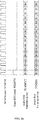
- PCM transmission timing in the related art is shown in Fig. 2a to Fig. 2d .
- Fig. 2a is a schematic transmission timing diagram illustrating Short Frame SYN Timing according to exemplary embodiment 1.
- Fig. 2b is a schematic transmission timing diagram illustrating Short Frame SYN Timing according to exemplary embodiment 2.
- Fig. 2c is a schematic transmission timing diagram illustrating Long Frame SYN Timing according to exemplary embodiment 1.
- Fig. 2d is a schematic transmission timing diagram illustrating Long Frame SYN Timing according to exemplary embodiment 2.
- PCMCLK is a pin corresponding to a bit synchronization (SYN) clock (also called a bit SYN clock pin).
- PCMSYN is a pin corresponding to a frame SYN clock (also called a frame SYN clock pin).
- PCMDOUT and PCMDIN are pins corresponding to audio data transmission lines (also called audio data transmission pins).
- the PCMDOUT is a pin corresponding to an audio data output line (also called an audio data output pin), and the PCMDIN is a pin corresponding to an audio data input line (also called an audio data input pin). Every time when PCMCLK vibrates for a cycle, a bit of data is transmitted on PCMDIN and PCMDOUT. Every time when PCMSYN vibrates for a cycle, a frame of data is transmitted.
- TDM transmission timing in the related art is shown in Fig. 3 .
- WS is a pin corresponding to a wakeup signal input by the TDM device (also called a wakeup signal pin)
- WSO represents an output signal for waking up a TDM device of a next stage after a TDM device of a previous stage completes transmitting one slot (also called a data transmission completion indication signal pin)
- SCK is a pin corresponding to a bit SYN signal (also called a bit SYN signal pin)
- SD is a pin corresponding to a data transmission line (also called a data transmission pin).
- the present-stage TDM device after receiving the WS which has a high-level pulse, may occupy a SD data transmission line to transmit one frame of data presently acquired by the present-stage TDM device, the one frame of data also being called one slot.
- WSO of a previous-stage device is required to be connected with the WS of a next-stage device. Every time when SCK vibrates for a cycle, a bit of data is transmitted on the SD data line.
- Different TDM devices may have different slot bit widths. Descriptions will be made in Fig. 3 with a slot bit width being 32 as an example.
- SCK is nx32xfs, where n is the number of cascading stages of the present-stage TDM device and fs is the sampling rate.
- WS in the TDM timing diagram is equivalent to PCMSYN in the PCM timing diagram.
- SCK in the TDM timing diagram is equivalent to PCMCLK in the PCM timing diagram.
- SD in the TDM timing diagram is equivalent to PCMDIN and/or PCMDOUT in the PCM timing diagram.
- WSO in the TDM timing diagram is a signal transmitted to a next-stage TDM device from a previous-stage TDM device, and is not required to correspond to the PCM timing. TDM devices are connected together stage by stage.
- the TDM devices may be connected through PCM interfaces.
- the types of peripherals supported by the master control chip may be extended.
- the technical solution of the present disclosure may be used, thereby avoiding additional use of more pins in the master control chip and avoiding increased complexity and cost of circuit wiring.
- a configuration parameter of new PCM timing (timing for connecting a TDM device) generated by the PCM controller may be associated with a sampling rate, a bit width occupied by data transmission of at least one TDM device and the number of the at least one TDM device plugged into the PCM interface corresponding to the PCM controller. Therefore, the PCM controller is configured according to the sampling rate, the bit width occupied by data transmission of the at least one TDM device and the number of the at least one TDM device plugged into the corresponding PCM interface corresponding to the PCM controller, and the at least one TDM device may be connected to the PCM interface at the PCM timing generated by the PCM controller and the data transmitted by the at least one TDM device may be acquired.
- a controller is configured according to a sampling rate, a bit width occupied by data transmission of a peripheral and the number of the peripheral plugged into an interface corresponding to the controller, and the data transmitted by the at least one peripheral plugged into the interface is received through the configured controller.
- a configuration parameter of the controller is reconfigured, and then the peripheral may be connected to the interface at the timing generated by the controller and the data transmitted by the at least one peripheral may be acquired, so that the types of the peripheral supported by the master control chip may be extended, and the number of the at least one peripheral that may be plugged into the master control chip is effectively increased.
- the operation S101 may include the following sub-operations A1-A2.
- a clock frequency of a bit SYN clock of the controller is acquired according to the sampling rate, the bit width and the number of the at least one peripheral.
- bit SYN clock is configured according to the clock frequency.
- the clock frequency of the bit SYN clock of the controller the bit width*the number of cascaded peripheral*the sampling rate.
- the clock frequency of the bit SYN clock is calculated through the formula, and the bit SYN clock is further configured based on the calculated clock frequency.
- the operation S101 may include the following sub-operations B1-B4.
- sub-operation B1 a clock cycle of the bit SYN clock is acquired according to the clock frequency of the bit SYN clock.
- sub-operation B2 a high pulse duration of a frame SYN clock of the controller is acquired according to the clock cycle of the bit SYN clock.
- a clock frequency of the frame SYN clock of the controller is acquired according to the sampling rate.
- the clock frequency of the frame SYN clock of the controller the sampling rate, i.e., the number of frames of data sampled per second.
- the frame SYN clock is configured according to the high pulse duration of the frame SYN clock and the clock frequency of the frame SYN clock.
- Transmission timing of the peripheral may be the same as transmission timing of the controller in some specific scenarios, and in such a case, the high pulse duration of the frame SYN clock is associated with the clock frequency of the frame SYN clock in the specific scenarios, so that it is necessary to configure the frame SYN clock according to the high pulse duration of the frame SYN clock and the clock frequency of the frame SYN clock.
- the operation S101 may include the following sub-operation that: a bit-width parameter of the controller is configured according to the bit width occupied by data transmission of the at least one peripheral.
- the bit width of the controller is set to be a bit width occupied by data transmission of one peripheral.
- the operation S101 may include the following sub-operation that: a parameter of the number of a sound track of the controller is configured according to the number of the at least one peripheral plugged into the interface.
- the peripheral may not generate a clock signal by itself, and thus the method may further include that: the controller is controlled to generate the frame SYN clock and the bit SYN clock.
- a preset clock mode of the controller is set, under which the controller generates the bit SYN clock and the frame SYN clock by itself for the peripheral to use.
- An embodiment of the present disclosure also provides a device for configuring a controller in a master control chip, which includes:
- the audio data output pin in the master control chip is connected with a data input pin of the first-stage peripheral.
- the audio data transmission pin in the master control chip includes an audio data input pin
- the audio data input pin in the master control chip is connected with a data output pin of the first-stage peripheral.
- a data transmission completion indication signal pin of a peripheral is connected with a wakeup signal pin of a next-stage peripheral; a bit SYN signal pin of the peripheral of each stage is connected with the bit SYN clock pin in the master control chip; and a data transmission pin of the peripheral of each stage may be connected with a data transmission pin in the master control chip.
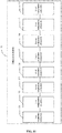
- Fig. 4 is a diagram illustrating a scenario according to an exemplary embodiment.
- Fig. 5 is a timing diagram of each pin in Fig. 4 according to an exemplary embodiment.
- a PCM controller is used as the controller in the master control chip and a PCM interface is used as the interface, all the TDM devices are cascaded.
- a PCMSYN pin in the PCM interface is connected with a WS pin of a first-stage TDM device, a PCMCLK pin in the PCM interface is connected with an SCK pin of the TDM device of each stage, and a PCMDIN pin in the PCM interface is connected with an SD pin of the TDM device of each stage.
- timing generated by the PCM controller corresponding to the PCM interface in the master control chip is the timing provided in the present disclosure.
- TDM devices can be connected to the master control chip which adopts the PCM transmission protocol only. Since all the TDM devices are cascaded, pins of the master control chip may be saved, and the complexity and cost of circuit wiring may be reduced. Moreover, a manufacturer of the master control chip may develop a TDM controller based on the original PCM controller and integrate it to the chip.
- the scenario in Fig. 4 is an example only.
- the PCMDOUT pin in the PCM interface may be connected with the SD pin of the TDM device of each stage; and if the TDM devices are output devices as well as input devices, the PCMDOUT pin in the PCM interface may be connected with the data input pin of the TDM device of each stage, and the PCMDIN pin in the PCM interface may be connected with the data output pin of the TDM device of each stage.
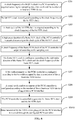
- Fig. 6 is a flow chart illustrating a method for configuring a controller in a master control chip according to an exemplary embodiment. As shown in Fig. 6 , the method includes the following operations.
- a clock frequency of a bit SYN clock of a PCM controller is acquired according to a sampling rate, a bit width and the number of at least one TDM device.
- the bit SYN clock is configured according to the clock frequency of the bit SYN clock.
- the clock frequency of PCMCLK is calculated through the formula, and the PCMCLK is further configured based on the calculated clock frequency of PCMCLK.
- a clock cycle of the bit SYN clock is acquired according to the clock frequency of the bit SYN clock.
- a high pulse duration of a frame SYN clock of the PCM controller is acquired according to the clock cycle of the bit SYN clock.
- a clock frequency of the frame SYN clock of the PCM controller is acquired according to the sampling rate.
- the clock frequency of the PCMSYN of the PCM controller the sampling rate, i.e., the number of frames of data sampled per second.
- the frame SYN clock is configured according to the high pulse duration of the frame SYN clock and the clock frequency of the frame SYN clock.
- TDM transmission timing is substantially the same as PCM Short Frame SYN Timing
- PCM controller outputs the Short Frame SYN Timing
- the high pulse duration of PCMSYN of the PCM controller one PCMCLK cycle.
- the clock frequency of the bit SYN clock is acquired in the above operations, the cycle of PCMCLK may be acquired based on the clock frequency of PCMCLK accordingly.
- a bit-width parameter of the PCM controller is configured according to the bit width occupied by data transmission of the at least one TDM device.
- the slot bit width of the PCM controller is set to be a bit width occupied by data transmission of one TDM device.
- a parameter of the number of a sound track of the PCM controller is configured according to the number of the at least one TDM device plugged into a PCM interface.
- the number of a PCM slot sound track of the PCM controller the number of the cascaded at least one TDM device.
- the PCM controller is controlled to generate the frame SYN clock and the bit SYN clock.
- a master clock mode of the PCM controller is set, namely the PCM controller generates the clocks PCMSYN and PCMCLK for the TDM device to use.
- the PCM controller is required to modify the slot bit width, i.e., a bit width occupied by each sampling point, according to requirements of different TDM devices, and the PCM controller is required to adjust the clock PCMCLK according to the number of the cascaded external TDM devices.
- the clock frequency of PCMCLK the slot bit width ⁇ the number of the cascaded at least one TDM device ⁇ the sampling rate of PCMSYN.
- the clock frequency of PCMSYN the sampling rate, and a Short Frame mode is adopted, namely the high-level pulse duration of PCMSYN is a PCMCLK cycle.
- the PCM controller serving as a master PCM clock, generates the clocks PCMSYN and PCMCLK.
- the number of slot sound tracks of the PCM controller the number of the cascaded TDM devices.
- a device embodiment of the present disclosure is provided below and may execute the method embodiment of the present disclosure.
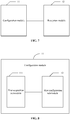
- Fig. 7 is a block diagram of a device for configuring a controller in a master control chip according to an exemplary embodiment. As shown in Fig. 7 , the device includes:
- the configuration module 11 includes a first acquisition submodule 111 and a first configuration submodule 112.
- the first acquisition submodule 111 is configured to acquire a clock frequency of a bit SYN clock of the controller according to the sampling rate, the bit width and the number of the at least one peripheral.
- the first configuration submodule 112 is configured to configure the bit SYN clock according to the clock frequency, acquired by the first acquisition submodule 111, of the bit SYN clock.
- the configuration module 11 includes a second acquisition submodule 113, a third acquisition submodule 114, a fourth acquisition submodule 115 and a second configuration submodule 116.
- the second acquisition submodule 113 is configured to acquire a clock cycle of the bit SYN clock according to the clock frequency, acquired by the first acquisition submodule 111, of the bit SYN clock.
- the third acquisition submodule 114 is configured to acquire a high pulse duration of a frame SYN clock of the controller according to the clock cycle, acquired by the second acquisition submodule 113, of the bit SYN clock.
- the fourth acquisition submodule 115 is configured to acquire a clock frequency of the frame SYN clock of the controller according to the sampling rate.
- the second configuration submodule 116 is configured to configure the frame SYN clock according to the high pulse duration, acquired by the third acquisition submodule 114, of the frame SYN clock and the clock frequency, acquired by the fourth acquisition submodule 115, of the frame SYN clock.
- the configuration module 11 includes a third configuration submodule 117.
- the third configuration submodule 117 is configured to configure a bit-width parameter of the controller according to the bit width occupied by data transmission of the at least one peripheral.
- the configuration module 11 includes a fourth configuration submodule 118.
- the fourth configuration submodule 118 is configured to configure a parameter of the number of a sound track of the controller according to the number of the at least one peripheral plugged into the interface.
- the device further includes a control submodule 119.
- the control submodule 119 is configured to control the controller to generate the frame SYN clock and the bit SYN clock.
- the controller may include a PCM controller; and the peripheral may include a TDM device.
- a device for configuring a controller in a master control chip which includes:
- the processor may further be configured to execute operations as follows.
- the processor may be further configured to:
- the processor may be further configured to:
- the processor may be further configured to: configure a bit-width parameter of the controller according to the bit width occupied by data transmission of the at least one peripheral.
- the processor may be further configured to: configure a parameter of the number of a sound track of the controller according to the number of the at least one peripheral plugged into the interface.
- the processor may further configured to: control the controller to generate the frame SYN clock and the bit SYN clock.
- the controller may include a PCM controller; and the peripheral may include a TDM device.
- Fig. 13 is a block diagram of a device 90 for configuring a controller in a master control chip according to an exemplary embodiment.
- the device 90 may act as a server.
- the device 90 may include: a processing component 902 which may further includes one or more processors; and a memory resource represented by a memory 903, configured to store an instruction executable by the processing component 902, for example, an application.
- the application stored in the memory 903 may include one or more than one module, each of which corresponds to a set of instructions.
- the processing component 902 is configured to execute the instruction to execute the abovementioned method.
- the device 90 may further include a power component 906 configured to execute power management of the device 90, a wired or wireless network interface 905 configured to connect the device 90 to a network and an Input/Output (I/O) interface 908.
- the device 90 may be operated based on an operating system stored in the memory 903, for example, Windows ServerTM, Max OS XTM, UnixTM, LinuxTM, FreeBSDTM or the like.
- non-transitory computer-readable storage medium having stored an instruction thereon, when executed by the processor of the device 90, to enable the device 90 to execute the method for configuring a controller in the master control chip, the method including that:
- the operation that the controller is configured according to the sampling rate, the bit width occupied by data transmission of the at least one peripheral and the number of the at least one peripheral plugged into the interface corresponding to the controller may include that:
- the operation that the controller is configured according to the sampling rate, the bit width occupied by data transmission of the at least one peripheral and the number of the at least one peripheral plugged into the interface corresponding to the controller may include that:
- the operation that the controller is configured according to the sampling rate, the bit width occupied by data transmission of the at least one peripheral and the number of the at least one peripheral plugged into the interface corresponding to the controller may include that: a bit-width parameter of the controller is configured according to the bit width occupied by data transmission of the at least one peripheral.
- the operation that the controller is configured according to the sampling rate, the bit width occupied by data transmission of the at least one peripheral and the number of the at least one peripheral plugged into the interface corresponding to the controller may include that: a parameter of the number of a sound track of the controller is configured according to the number of the at least one peripheral plugged into the interface.
- the method further may include that: the controller is controlled to generate the frame SYN clock and the bit SYN clock.
- the controller may include a PCM controller; and the peripheral may include a TDM device.
Landscapes
- Engineering & Computer Science (AREA)
- Theoretical Computer Science (AREA)
- Physics & Mathematics (AREA)
- General Engineering & Computer Science (AREA)
- General Physics & Mathematics (AREA)
- Computer Hardware Design (AREA)
- Microelectronics & Electronic Packaging (AREA)
- Time-Division Multiplex Systems (AREA)
- Information Transfer Systems (AREA)
- Synchronisation In Digital Transmission Systems (AREA)
Abstract
Description
- The present disclosure generally relates to the technical field of communications, and more particularly, to a method and device for configuring a controller in a master control chip.
- A master control chip, which is a core component of a main board or a hard disk, is a bridge for connecting each device and also a brain for controlling a device to run and work. At present, many master control chips have external interfaces for preset peripherals for being plugged into. During use, the preset peripherals are only required to be plugged into the external interfaces of the master control chips.
- For solving the problem in a related art, embodiments of the present disclosure provide a method and device for configuring a controller in a master control chip. The technical solutions are implemented as follows.
- According to a first aspect of the embodiments of the present disclosure, a method for configuring a controller in a master control chip is provided, which may include that:
- a controller is configured according to a sampling rate, a bit width occupied by data transmission of at least one peripheral and the number of the at least one peripheral plugged into an interface corresponding to the controller; and
- data transmitted by the at least one peripheral plugged into the interface is received through the configured controller.
- The technical solution provided in the embodiments of the present disclosure may have the following beneficial effects. The controller is configured according to the sampling rate, the bit width occupied by data transmission of the at least one peripheral and the number of the at least one peripheral plugged into the interface corresponding to the controller, and the data transmitted by the peripheral plugged into the interface is received through the configured controller. A configuration parameter of the controller is reconfigured, and then peripheral may be connected to the interface at the timing generated by the controller and the data transmitted by the peripheral may be acquired, so that types of peripherals supported by the master control chip are extended, and the number of peripherals that can be plugged into the master control chip is effectively increased.
- In an embodiment, the operation that the controller is configured according to the sampling rate, the bit width occupied by data transmission of the at least one peripheral and the number of the at least one peripheral plugged into the interface corresponding to the controller may include that:
- a clock frequency of a bit Synchronization (SYN) clock of the controller is acquired according to the sampling rate, the bit width and the number of the at least one peripheral; and
- the bit SYN clock is configured according to the clock frequency of the bit SYN clock.
- In an embodiment, the operation that the controller is configured according to the sampling rate, the bit width occupied by data transmission of the at least one peripheral and the number of the at least one peripheral plugged into the interface corresponding to the controller may include that:
- a clock cycle of the bit SYN clock is acquired according to the clock frequency of the bit SYN clock;
- a high pulse duration of a frame SYN clock of the controller is acquired according to the clock cycle of the bit SYN clock;
- a clock frequency of the frame SYN clock of the controller is acquired according to the sampling rate; and
- the frame SYN clock is configured according to the high pulse duration of the frame SYN clock and the clock frequency of the frame SYN clock.
- In an embodiment, the operation that the controller is configured according to the sampling rate, the bit width occupied by data transmission of the at least one peripheral and the number of the at least one peripheral plugged into the interface corresponding to the controller may include that:
a bit-width parameter of the controller is configured according to the bit width occupied by data transmission of the peripheral. - In an embodiment, the operation that the controller is configured according to the sampling rate, the bit width occupied by data transmission of the at least one peripheral and the number of the at least one peripheral plugged into the interface corresponding to the controller may include that:
a parameter of the number of a sound track of the controller is configured according to the number of the at least one peripheral plugged into the interface. - In an embodiment, the method may further include that:
the controller is controlled to generate the frame SYN clock and the bit SYN clock. - In an embodiment, the controller may include a Pulse Code Modulation (PCM) controller; and the peripheral may include a Time Division Multiplexing (TDM) device.
- According to a second aspect of the embodiments of the present disclosure, a device for configuring a controller in a master control chip is provided, which may include:
- a configuration module, configured to configure a controller according to a sampling rate, a bit width occupied by data transmission of at least one peripheral and the number of the at least one peripheral plugged into an interface corresponding to the controller; and
- a reception module, configured to receive data transmitted by the peripheral plugged into the interface through the controller configured by the configuration module.
- In an embodiment, the configuration module may include a first acquisition submodule and a first configuration submodule.
- The first acquisition submodule may be configured to acquire a clock frequency of a bit SYN clock of the controller according to the sampling rate, the bit width and the number of the at least one peripheral.
- The first configuration submodule may be configured to configure the bit SYN clock according to the clock frequency, acquired by the first acquisition submodule, of the bit SYN clock.
- In an embodiment, the configuration module may include a second acquisition submodule, a third acquisition submodule, a fourth acquisition submodule and a second configuration submodule.
- The second acquisition submodule may be configured to acquire a clock cycle of the bit SYN clock according to the clock frequency, acquired by the first acquisition submodule, of the bit SYN clock.
- The third acquisition submodule may be configured to acquire a high pulse duration of a frame SYN clock of the controller according to the clock cycle, acquired by the second acquisition submodule, of the bit SYN clock.
- The fourth acquisition submodule may be configured to acquire a clock frequency of the frame SYN clock of the controller according to the sampling rate.
- The second configuration submodule may be configured to configure the frame SYN clock according to the high pulse duration, acquired by the third acquisition submodule, of the frame SYN clock and the clock frequency, acquired by the fourth acquisition submodule, of the frame SYN clock.
- In an embodiment, the configuration module may include a third configuration submodule.
- The third configuration submodule may be configured to configure a bit-width parameter of the controller according to the bit width occupied by data transmission of the peripheral.
- In an embodiment, the configuration module may include a fourth configuration submodule.
- The fourth configuration submodule may be configured to configure a parameter of the number of a sound track of the controller according to the number of the at least one peripheral plugged into the interface.
- In an embodiment, the device may further include a control submodule.
- The control submodule may be configured to control the controller to generate the frame SYN clock and the bit SYN clock.
- In an embodiment, the controller may include a PCM controller; and the peripheral may include a TDM device.
- According to a third aspect of the embodiments of the present disclosure, a device for configuring a controller in a master control chip is provided, which may include:
- the master control chip and N cascaded peripherals, N being a positive integer more than or equal to 1, wherein
- a frame SYN clock pin in the master control chip may be connected with a wakeup signal pin of a first-stage peripheral, the first-stage peripheral being one of the N peripherals;
- a bit SYN clock pin in the master control chip may be connected with a bit SYN signal pin of the first-stage peripheral; and
- an audio data transmission pin in the master control chip may be connected with a data transmission pin of the first-stage peripheral.
- In an embodiment, an audio data output pin in the master control chip may be connected with a data input pin of the first-stage peripheral; and an audio data input pin in the master control chip may be connected with a data output pin of the first-stage peripheral.
- In an embodiment, for the N cascaded peripherals, a data transmission completion indication signal pin of a previous-stage peripheral may be connected with a wakeup signal pin of a next-stage peripheral of the previous-stage peripheral;
a bit SYN signal pin of a peripheral of each stage may be connected with the bit SYN clock pin in the master control chip; and
a data transmission pin of the peripheral of each stage may be connected with a data transmission pin in the master control chip. - In an embodiment, a controller in the master control chip may include a PCM controller; and the peripheral may include a TDM device.
- According to a fourth aspect of the embodiments of the present disclosure, a device for configuring a controller in a master control chip is provided, which may include:
- a processor; and
- a memory configured to store an instruction executable by the processor,
- wherein the processor may be configured to:
- configure a controller according to a sampling rate, a bit width occupied by data transmission of at least one peripheral and the number of the at least one peripheral plugged into an interface corresponding to the controller; and
- receive data transmitted by the at least one peripheral plugged into the interface through the configured controller.
- According to a fifth aspect of the embodiments of the present disclosure, a computer-readable storage medium is provided, which have stored a computer instruction thereon, the instruction when executed by a processor, enabling the processor to implement the operations of any method in the first aspect.
- It is to be understood that the above general descriptions and detailed descriptions below are only exemplary and explanatory and not intended to limit the present disclosure.
- The accompanying drawings, which are incorporated in and constitute a part of this specification, illustrate embodiments consistent with the present disclosure and, together with the description, serve to explain the principles of the present disclosure.
-
Fig. 1 is a flow chart illustrating a method for configuring a controller in a master control chip according to an exemplary embodiment. -
Fig. 2a is a schematic transmission timing diagram illustrating Short Frame SYN Timing according toexemplary embodiment 1. -
Fig. 2b is a schematic transmission timing diagram illustrating Short Frame SYN Timing according toexemplary embodiment 2. -
Fig. 2c is a schematic transmission timing diagram illustrating Long Frame SYN Timing according toexemplary embodiment 1. -
Fig. 2d is a schematic transmission timing diagram illustrating Long Frame SYN Timing according toexemplary embodiment 2. -
Fig. 3 is a schematic diagram illustrating TDM transmission timing according toexemplary embodiment 2. -
Fig. 4 is a diagram illustrating a scenario according to an exemplary embodiment. -
Fig. 5 is a timing diagram of each pin inFig. 4 according to an exemplary embodiment. -
Fig. 6 is a flow chart illustrating a method for configuring a controller in a master control chip according to an exemplary embodiment. -
Fig. 7 is a block diagram of a device for configuring a controller in a master control chip according to an exemplary embodiment. -
Fig. 8 is a block diagram of a configuration module in a device for configuring a controller in a master control chip according to an exemplary embodiment. -
Fig. 9 is a block diagram of a configuration module in a device for configuring a controller in a master control chip according to an exemplary embodiment. -
Fig. 10 is a block diagram of a configuration module in a device for configuring a controller in a master control chip according to an exemplary embodiment. -
Fig. 11 is a block diagram of a configuration module in a device for configuring a controller in a master control chip according to an exemplary embodiment. -
Fig. 12 is a block diagram of a configuration module in a device for configuring a controller in a master control chip according to an exemplary embodiment. -
Fig. 13 is a block diagram of a device 90 for configuring a controller in a master control chip according to an exemplary embodiment. - Reference will now be made in detail to exemplary embodiments, examples of which are illustrated in the accompanying drawings. The following description refers to the accompanying drawings in which the same numbers in different drawings represent the same or similar elements unless otherwise represented. The implementations set forth in the following description of exemplary embodiments do not represent all implementations consistent with the present disclosure. Instead, they are merely examples of apparatuses and methods consistent with aspects associated with the present disclosure as recited in the appended claims.
- Terms used in the present disclosure are only adopted for the purpose of describing specific embodiments but not intended to limit the present disclosure. It is also to be understood that term "and/or" used in the present disclosure refers to and includes one or any or all possible combinations of multiple associated items that are listed.
- It is to be understood that "first", "second" and similar terms used in the specification and claims of the present application are not to represent any sequence, number or importance but only to distinguish different parts. Likewise, similar terms such as "a/an" and "the" as well as the plurality form do not represent a number limit but represent "at least one". Terms like "include" or "comprise" refer to that an element or object appearing before "include" or "comprise" covers an element or object and equivalent thereof listed after "include" or "comprise" and does not exclude another element or object.
- Many master control chips have external interfaces for preset peripherals to be plugged in. During use, the preset peripherals are required to be plugged into the external interfaces of the master control chip only. However, the type of existing external interfaces in master control chips is undiversified, which cannot flexibly support plugging of peripherals of other types. For example, an external interface only supports plugging of a peripheral of a first type while cannot support plugging of a peripheral of a second type.
- The present disclosure may provide a method for achieving compatibility between a transmission protocol of an external interface and transmission protocols of other peripherals, so that the types of peripherals supported by a master control chip may be extended.
- For example, for connecting multiple sound recording devices, it is usually necessary to use a fixed audio transmission protocol, such as an Inter-Integrated Circuit Sound (I2S) protocol. The I2S protocol is a bus standard that is set by Philips for audio data transmission between digital audio devices, and the bus is dedicated to data transmission between audio devices. However, according to the I2S protocol, a single data line can be used for transmitting dual-track audio data only, and for transmission of audio data of more sound tracks, more data lines are needed, so that the number of occupied pins of a master control chip may be increased, and complexity and cost of circuit wiring may also be increased.
- However, a Time Division Multiplexing (TDM) transmission protocol has the characteristics that only a few pins are occupied, many devices can be cascaded and multiple devices multiplex a data line in a time division manner. Therefore, multiple external TDM devices, for example, TDM Digital Microphones (DMICs), may be simply connected with a master control chip through the TDM transmission protocol so as to transmit more sound tracks without additionally using more pins in the master control chip.
- At present, there are few master control chips with TDM interfaces, however, many master control chips have Pulse Code Modulation (PCM) transmission interfaces. Accordingly, the present disclosure may provide a method for achieving compatibility between a PCM transmission protocol and a TDM transmission protocol, so that the types of peripherals capable of being supported by a master control chip may be extended. In some scenarios, for example, a master control chip is connected with an external TDM DMIC array, the method of the present disclosure may be used.
-
Fig. 1 is a flow chart illustrating a method for configuring a controller in a master control chip according to an exemplary embodiment. As shown inFig. 1 , the method includes the following operations S101 to S102. - In operation S101, a controller is configured according to a sampling rate, a bit width occupied by data transmission of at least one peripheral and the number of the at least one peripheral plugged into an interface corresponding to the controller.
- In operation S102, data transmitted by the at least one peripheral plugged into the interface is received through the configured controller.
- For describing the concept of the present disclosure clearly, descriptions will be made below with the condition that the controller includes a PCM controller and the peripheral includes a TDM device as an example. It is to be noted that, in a practical application, the controller and the peripheral may also be of other types.
- The master control chip may usually be integrated with a PCM protocol controller for connecting with an external PCM device.
- PCM transmission timing in the related art is shown in
Fig. 2a to Fig. 2d . -
Fig. 2a is a schematic transmission timing diagram illustrating Short Frame SYN Timing according toexemplary embodiment 1.Fig. 2b is a schematic transmission timing diagram illustrating Short Frame SYN Timing according toexemplary embodiment 2.Fig. 2c is a schematic transmission timing diagram illustrating Long Frame SYN Timing according toexemplary embodiment 1.Fig. 2d is a schematic transmission timing diagram illustrating Long Frame SYN Timing according toexemplary embodiment 2. InFig. 2a to Fig. 2d , descriptions are made with the condition that a bit width is 16bit as an example, and each of B0 to B15 represents one bit. PCMCLK is a pin corresponding to a bit synchronization (SYN) clock (also called a bit SYN clock pin). PCMSYN is a pin corresponding to a frame SYN clock (also called a frame SYN clock pin). PCMDOUT and PCMDIN are pins corresponding to audio data transmission lines (also called audio data transmission pins). The PCMDOUT is a pin corresponding to an audio data output line (also called an audio data output pin), and the PCMDIN is a pin corresponding to an audio data input line (also called an audio data input pin). Every time when PCMCLK vibrates for a cycle, a bit of data is transmitted on PCMDIN and PCMDOUT. Every time when PCMSYN vibrates for a cycle, a frame of data is transmitted. - TDM transmission timing in the related art is shown in
Fig. 3 . - WS is a pin corresponding to a wakeup signal input by the TDM device (also called a wakeup signal pin), WSO represents an output signal for waking up a TDM device of a next stage after a TDM device of a previous stage completes transmitting one slot (also called a data transmission completion indication signal pin), SCK is a pin corresponding to a bit SYN signal (also called a bit SYN signal pin), and SD is a pin corresponding to a data transmission line (also called a data transmission pin).
- The present-stage TDM device, after receiving the WS which has a high-level pulse, may occupy a SD data transmission line to transmit one frame of data presently acquired by the present-stage TDM device, the one frame of data also being called one slot. WSO of a previous-stage device is required to be connected with the WS of a next-stage device. Every time when SCK vibrates for a cycle, a bit of data is transmitted on the SD data line.
- Different TDM devices may have different slot bit widths. Descriptions will be made in
Fig. 3 with a slot bit width being 32 as an example. In such a case, SCK is nx32xfs, where n is the number of cascading stages of the present-stage TDM device and fs is the sampling rate. - It can be seen from
Fig. 2a to Fig. 3 that the TDM transmission timing is substantially the same as the PCM Short Frame SYN Timing. - That is, WS in the TDM timing diagram is equivalent to PCMSYN in the PCM timing diagram. SCK in the TDM timing diagram is equivalent to PCMCLK in the PCM timing diagram. SD in the TDM timing diagram is equivalent to PCMDIN and/or PCMDOUT in the PCM timing diagram. WSO in the TDM timing diagram is a signal transmitted to a next-stage TDM device from a previous-stage TDM device, and is not required to correspond to the PCM timing. TDM devices are connected together stage by stage.
- At present, many master control chips have PCM interfaces, but most of them do not have TDM interfaces. Since transmission timing of the PCM transmission protocol and that of the TDM transmission protocol are substantially the same in the abovementioned special scenario, the TDM devices may be connected through PCM interfaces.
- Accordingly, the types of peripherals supported by the master control chip may be extended. In some scenarios, for example, when the master control chip is connected with an external TDM DMIC array, the technical solution of the present disclosure may be used, thereby avoiding additional use of more pins in the master control chip and avoiding increased complexity and cost of circuit wiring.
- A configuration parameter of new PCM timing (timing for connecting a TDM device) generated by the PCM controller may be associated with a sampling rate, a bit width occupied by data transmission of at least one TDM device and the number of the at least one TDM device plugged into the PCM interface corresponding to the PCM controller. Therefore, the PCM controller is configured according to the sampling rate, the bit width occupied by data transmission of the at least one TDM device and the number of the at least one TDM device plugged into the corresponding PCM interface corresponding to the PCM controller, and the at least one TDM device may be connected to the PCM interface at the PCM timing generated by the PCM controller and the data transmitted by the at least one TDM device may be acquired.
- The technical solution provided in the embodiment of the present disclosure may have the following beneficial effects. A controller is configured according to a sampling rate, a bit width occupied by data transmission of a peripheral and the number of the peripheral plugged into an interface corresponding to the controller, and the data transmitted by the at least one peripheral plugged into the interface is received through the configured controller. A configuration parameter of the controller is reconfigured, and then the peripheral may be connected to the interface at the timing generated by the controller and the data transmitted by the at least one peripheral may be acquired, so that the types of the peripheral supported by the master control chip may be extended, and the number of the at least one peripheral that may be plugged into the master control chip is effectively increased.
- In an embodiment, the operation S101 may include the following sub-operations A1-A2.
- In sub-operation A1, a clock frequency of a bit SYN clock of the controller is acquired according to the sampling rate, the bit width and the number of the at least one peripheral.
- In sub-operation A2, the bit SYN clock is configured according to the clock frequency.
- Exemplarily, it is set that the clock frequency of the bit SYN clock of the controller=the bit width*the number of cascaded peripheral*the sampling rate. The clock frequency of the bit SYN clock is calculated through the formula, and the bit SYN clock is further configured based on the calculated clock frequency.
- In an embodiment, the operation S101 may include the following sub-operations B1-B4.
- In sub-operation B1, a clock cycle of the bit SYN clock is acquired according to the clock frequency of the bit SYN clock.
- In sub-operation B2, a high pulse duration of a frame SYN clock of the controller is acquired according to the clock cycle of the bit SYN clock.
- In sub-operation B3, a clock frequency of the frame SYN clock of the controller is acquired according to the sampling rate.
- It is set that the clock frequency of the frame SYN clock of the controller=the sampling rate, i.e., the number of frames of data sampled per second.
- In sub-operation B4, the frame SYN clock is configured according to the high pulse duration of the frame SYN clock and the clock frequency of the frame SYN clock.
- Transmission timing of the peripheral may be the same as transmission timing of the controller in some specific scenarios, and in such a case, the high pulse duration of the frame SYN clock is associated with the clock frequency of the frame SYN clock in the specific scenarios, so that it is necessary to configure the frame SYN clock according to the high pulse duration of the frame SYN clock and the clock frequency of the frame SYN clock.
- In an embodiment, the operation S101 may include the following sub-operation that:
a bit-width parameter of the controller is configured according to the bit width occupied by data transmission of the at least one peripheral. - The bit width of the controller is set to be a bit width occupied by data transmission of one peripheral.
- In an embodiment, the operation S101 may include the following sub-operation that:
a parameter of the number of a sound track of the controller is configured according to the number of the at least one peripheral plugged into the interface. - It is set that the sound track number of the controller=the number of the cascaded peripherals.
- In an embodiment, the peripheral may not generate a clock signal by itself, and thus the method may further include that:
the controller is controlled to generate the frame SYN clock and the bit SYN clock. - A preset clock mode of the controller is set, under which the controller generates the bit SYN clock and the frame SYN clock by itself for the peripheral to use.
- An embodiment of the present disclosure also provides a device for configuring a controller in a master control chip, which includes:
- a master control chip and N cascaded peripherals, N being a positive integer more than or equal to 1, wherein
- a frame SYN clock pin in the master control chip is connected with a wakeup signal pin of a first-stage peripheral, the first-stage peripheral being one of the N peripherals;
- a bit SYN clock pin in the master control chip is connected with a bit SYN signal pin of the first-stage peripheral; and
- an audio data transmission pin in the master control chip is connected with a data transmission pin of the first-stage peripheral.
- When the audio data transmission pin in the master control chip includes an audio data output pin, the audio data output pin in the master control chip is connected with a data input pin of the first-stage peripheral.
- When the audio data transmission pin in the master control chip includes an audio data input pin, the audio data input pin in the master control chip is connected with a data output pin of the first-stage peripheral.
- In an implementation mode, for the N cascaded peripherals, a data transmission completion indication signal pin of a peripheral is connected with a wakeup signal pin of a next-stage peripheral;
a bit SYN signal pin of the peripheral of each stage is connected with the bit SYN clock pin in the master control chip; and
a data transmission pin of the peripheral of each stage may be connected with a data transmission pin in the master control chip. -
Fig. 4 is a diagram illustrating a scenario according to an exemplary embodiment.Fig. 5 is a timing diagram of each pin inFig. 4 according to an exemplary embodiment. As shown inFig. 4 to Fig. 5 , in the scenario where ICS-52000 TDM devices are used as peripherals, a PCM controller is used as the controller in the master control chip and a PCM interface is used as the interface, all the TDM devices are cascaded. A PCMSYN pin in the PCM interface is connected with a WS pin of a first-stage TDM device, a PCMCLK pin in the PCM interface is connected with an SCK pin of the TDM device of each stage, and a PCMDIN pin in the PCM interface is connected with an SD pin of the TDM device of each stage. In such a case, timing generated by the PCM controller corresponding to the PCM interface in the master control chip is the timing provided in the present disclosure. - Through the method in the present disclosure, TDM devices can be connected to the master control chip which adopts the PCM transmission protocol only. Since all the TDM devices are cascaded, pins of the master control chip may be saved, and the complexity and cost of circuit wiring may be reduced. Moreover, a manufacturer of the master control chip may develop a TDM controller based on the original PCM controller and integrate it to the chip.
- It is to be noted that the scenario in
Fig. 4 is an example only. During the practical application, if TDM devices are output devices, the PCMDOUT pin in the PCM interface may be connected with the SD pin of the TDM device of each stage; and if the TDM devices are output devices as well as input devices, the PCMDOUT pin in the PCM interface may be connected with the data input pin of the TDM device of each stage, and the PCMDIN pin in the PCM interface may be connected with the data output pin of the TDM device of each stage. There are no limits made thereto in the present disclosure. -
Fig. 6 is a flow chart illustrating a method for configuring a controller in a master control chip according to an exemplary embodiment. As shown inFig. 6 , the method includes the following operations. - In operation S201, a clock frequency of a bit SYN clock of a PCM controller is acquired according to a sampling rate, a bit width and the number of at least one TDM device.
- In operation S202, the bit SYN clock is configured according to the clock frequency of the bit SYN clock.
- Exemplarily, it is set that the clock frequency of PCMCLK of the PCM controller=the slot bit width*the number of cascaded at least one TDM device*the sampling rate of PCMSYN. The clock frequency of PCMCLK is calculated through the formula, and the PCMCLK is further configured based on the calculated clock frequency of PCMCLK.
- In operation S203, a clock cycle of the bit SYN clock is acquired according to the clock frequency of the bit SYN clock.
- In operation S204, a high pulse duration of a frame SYN clock of the PCM controller is acquired according to the clock cycle of the bit SYN clock.
- In operation S205, a clock frequency of the frame SYN clock of the PCM controller is acquired according to the sampling rate.
- It is set that the clock frequency of the PCMSYN of the PCM controller=the sampling rate, i.e., the number of frames of data sampled per second.
- In operation S206, the frame SYN clock is configured according to the high pulse duration of the frame SYN clock and the clock frequency of the frame SYN clock.
- Since TDM transmission timing is substantially the same as PCM Short Frame SYN Timing, it is necessary to configure that the PCM controller outputs the Short Frame SYN Timing, and in such a case, it is necessary to set that the high pulse duration of PCMSYN of the PCM controller=one PCMCLK cycle. The clock frequency of the bit SYN clock is acquired in the above operations, the cycle of PCMCLK may be acquired based on the clock frequency of PCMCLK accordingly.
- In operation S207, a bit-width parameter of the PCM controller is configured according to the bit width occupied by data transmission of the at least one TDM device.
- The slot bit width of the PCM controller is set to be a bit width occupied by data transmission of one TDM device.
- In operation S208, a parameter of the number of a sound track of the PCM controller is configured according to the number of the at least one TDM device plugged into a PCM interface.
- It is set that the number of a PCM slot sound track of the PCM controller=the number of the cascaded at least one TDM device.
- In operation S209, the PCM controller is controlled to generate the frame SYN clock and the bit SYN clock.
- Since the TDM device cannot generate a clock signal by itself, a master clock mode of the PCM controller is set, namely the PCM controller generates the clocks PCMSYN and PCMCLK for the TDM device to use.
- In operation S2010, data transmitted by the at least one TDM device plugged into the PCM interface is received through the configured PCM controller.
- In the present disclosure, since Short Frame SYN Timing of PCM transmission timing and the TDM transmission timing are substantially the same and can be compatible, the PCM controller is required to modify the slot bit width, i.e., a bit width occupied by each sampling point, according to requirements of different TDM devices, and the PCM controller is required to adjust the clock PCMCLK according to the number of the cascaded external TDM devices. The clock frequency of PCMCLK=the slot bit width × the number of the cascaded at least one TDM device × the sampling rate of PCMSYN. The clock frequency of PCMSYN=the sampling rate, and a Short Frame mode is adopted, namely the high-level pulse duration of PCMSYN is a PCMCLK cycle. The PCM controller, serving as a master PCM clock, generates the clocks PCMSYN and PCMCLK. The number of slot sound tracks of the PCM controller=the number of the cascaded TDM devices.
- A device embodiment of the present disclosure is provided below and may execute the method embodiment of the present disclosure.
-
Fig. 7 is a block diagram of a device for configuring a controller in a master control chip according to an exemplary embodiment. As shown inFig. 7 , the device includes: - a
configuration module 11, configured to configure a controller according to a sampling rate, a bit width occupied by data transmission of at least one peripheral and the number of the at least one peripheral plugged into an interface corresponding to the controller; and - a
reception module 12, configured to receive data transmitted by the at least one peripheral plugged into the interface through the controller configured by theconfiguration module 11. - In an embodiment, as shown in
Fig. 8 , theconfiguration module 11 includes afirst acquisition submodule 111 and afirst configuration submodule 112. - The
first acquisition submodule 111 is configured to acquire a clock frequency of a bit SYN clock of the controller according to the sampling rate, the bit width and the number of the at least one peripheral. - The
first configuration submodule 112 is configured to configure the bit SYN clock according to the clock frequency, acquired by thefirst acquisition submodule 111, of the bit SYN clock. - In an embodiment, as shown in
Fig. 9 , theconfiguration module 11 includes asecond acquisition submodule 113, athird acquisition submodule 114, afourth acquisition submodule 115 and asecond configuration submodule 116. - The
second acquisition submodule 113 is configured to acquire a clock cycle of the bit SYN clock according to the clock frequency, acquired by thefirst acquisition submodule 111, of the bit SYN clock. - The
third acquisition submodule 114 is configured to acquire a high pulse duration of a frame SYN clock of the controller according to the clock cycle, acquired by thesecond acquisition submodule 113, of the bit SYN clock. - The
fourth acquisition submodule 115 is configured to acquire a clock frequency of the frame SYN clock of the controller according to the sampling rate. - The
second configuration submodule 116 is configured to configure the frame SYN clock according to the high pulse duration, acquired by thethird acquisition submodule 114, of the frame SYN clock and the clock frequency, acquired by thefourth acquisition submodule 115, of the frame SYN clock. - In an embodiment, as shown in
Fig. 10 , theconfiguration module 11 includes athird configuration submodule 117. - The
third configuration submodule 117 is configured to configure a bit-width parameter of the controller according to the bit width occupied by data transmission of the at least one peripheral. - In an embodiment, as shown in
Fig. 11 , theconfiguration module 11 includes afourth configuration submodule 118. - The
fourth configuration submodule 118 is configured to configure a parameter of the number of a sound track of the controller according to the number of the at least one peripheral plugged into the interface. - In an embodiment, as shown in
Fig. 12 , the device further includes acontrol submodule 119. - The control submodule 119 is configured to control the controller to generate the frame SYN clock and the bit SYN clock.
- In an embodiment, the controller may include a PCM controller; and the peripheral may include a TDM device.
- According to a third aspect of the embodiments of the present disclosure, a device for configuring a controller in a master control chip is provided, which includes:
- a processor; and
- a memory configured to store an instruction executable by the processor,
- wherein the processor is configured to:
- configure a controller according to a sampling rate, a bit width occupied by data transmission of at least one peripheral and the number of the at least one peripheral plugged into an interface corresponding to the controller; and
- control a transceiver to receive data transmitted by the at least one peripheral plugged into the interface through the configured controller.
- The processor may further be configured to execute operations as follows.
- For the operation that the controller is configured according to the sampling rate, the bit width occupied by data transmission of the at least one peripheral and the number of the at least one peripheral plugged into the interface corresponding to the controller, the processor may be further configured to:
- acquire a clock frequency of a bit SYN clock of the controller according to the sampling rate, the bit width and the number of the at least one peripheral; and
- configuring the bit SYN clock according to the clock frequency of the bit SYN clock.
- For the operation that the controller is configured according to the sampling rate, the bit width occupied by data transmission of the at least one peripheral and the number of the at least one peripheral plugged into the interface corresponding to the controller, the processor may be further configured to:
- acquire a clock cycle of the bit SYN clock according to the clock frequency of the bit SYN clock;
- acquire a high pulse duration of a frame SYN clock of the controller according to the clock cycle of the bit SYN clock;
- acquire a clock frequency of the frame SYN clock of the controller according to the sampling rate; and
- configure the frame SYN clock according to the high pulse duration of the frame SYN clock and the clock frequency of the frame SYN clock.
- For the operation that the controller is configured according to the sampling rate, the bit width occupied by data transmission of the at least one peripheral and the number of the at least one peripheral plugged into the interface corresponding to the controller, the processor may be further configured to:
configure a bit-width parameter of the controller according to the bit width occupied by data transmission of the at least one peripheral. - For the operation that the controller is configured according to the sampling rate, the bit width occupied by data transmission of the at least one peripheral and the number of the at least one peripheral plugged into the interface corresponding to the controller, the processor may be further configured to:
configure a parameter of the number of a sound track of the controller according to the number of the at least one peripheral plugged into the interface. - The processor may further configured to:
control the controller to generate the frame SYN clock and the bit SYN clock. - The controller may include a PCM controller; and the peripheral may include a TDM device.
- With respect to the device in the above embodiment, the specific manners for performing operations of individual components therein have been described in detail in the embodiment of the method, which will not be elaborated herein.
-
Fig. 13 is a block diagram of a device 90 for configuring a controller in a master control chip according to an exemplary embodiment. For example, the device 90 may act as a server. The device 90 may include: aprocessing component 902 which may further includes one or more processors; and a memory resource represented by amemory 903, configured to store an instruction executable by theprocessing component 902, for example, an application. The application stored in thememory 903 may include one or more than one module, each of which corresponds to a set of instructions. In addition, theprocessing component 902 is configured to execute the instruction to execute the abovementioned method. - The device 90 may further include a
power component 906 configured to execute power management of the device 90, a wired orwireless network interface 905 configured to connect the device 90 to a network and an Input/Output (I/O)interface 908. The device 90 may be operated based on an operating system stored in thememory 903, for example, Windows ServerTM, Max OS XTM, UnixTM, LinuxTM, FreeBSDTM or the like. - According to a non-transitory computer-readable storage medium, having stored an instruction thereon, when executed by the processor of the device 90, to enable the device 90 to execute the method for configuring a controller in the master control chip, the method including that:
- a controller is configured according to a sampling rate, a bit width occupied by data transmission of at least one peripheral and the number of the at least one peripheral plugged into an interface corresponding to the controller; and
- data transmitted by the at least one peripheral plugged into the interface is received through the configured controller.
- The operation that the controller is configured according to the sampling rate, the bit width occupied by data transmission of the at least one peripheral and the number of the at least one peripheral plugged into the interface corresponding to the controller may include that:
- a clock frequency of a bit SYN clock of the controller is acquired according to the sampling rate, the bit width and the number of the at least one peripheral; and
- the bit SYN clock is configured according to the clock frequency of the bit SYN clock.
- The operation that the controller is configured according to the sampling rate, the bit width occupied by data transmission of the at least one peripheral and the number of the at least one peripheral plugged into the interface corresponding to the controller may include that:
- a clock cycle of the bit SYN clock is acquired according to the clock frequency of the bit SYN clock;
- a high pulse duration of a frame SYN clock of the controller is acquired according to the clock cycle of the bit SYN clock;
- a clock frequency of the frame SYN clock of the controller is acquired according to the sampling rate; and
- the frame SYN clock is configured according to the high pulse duration of the frame SYN clock and the clock frequency of the frame SYN clock.
- The operation that the controller is configured according to the sampling rate, the bit width occupied by data transmission of the at least one peripheral and the number of the at least one peripheral plugged into the interface corresponding to the controller may include that:
a bit-width parameter of the controller is configured according to the bit width occupied by data transmission of the at least one peripheral. - The operation that the controller is configured according to the sampling rate, the bit width occupied by data transmission of the at least one peripheral and the number of the at least one peripheral plugged into the interface corresponding to the controller may include that:
a parameter of the number of a sound track of the controller is configured according to the number of the at least one peripheral plugged into the interface. - The method further may include that:
the controller is controlled to generate the frame SYN clock and the bit SYN clock. - The controller may include a PCM controller; and the peripheral may include a TDM device.
- Other implementation solutions of the present disclosure will be apparent to those skilled in the art from consideration of the specification and practice of the present disclosure. This application is intended to cover any variations, uses, or adaptations of the present disclosure following the general principles thereof and including such departures from the present disclosure as come within known or customary practice in the art. It is intended that the specification and examples be considered as exemplary only, with a true scope of the present disclosure being indicated by the following claims.
- It will be appreciated that the present disclosure is not limited to the exact construction that has been described above and illustrated in the accompanying drawings, and that various modifications and changes may be made without departing from the scope thereof. It is intended that the scope of the present disclosure only be limited by the appended claims.
Claims (15)
- A method for configuring a controller in a master control chip, comprising:configuring a controller according to a sampling rate, a bit width occupied by data transmission of at least one peripheral and the number of the at least one peripheral plugged into an interface corresponding to the controller; andreceiving data transmitted by the at least one peripheral plugged into the interface through the controller.
- The method of claim 1, wherein configuring the controller according to the sampling rate, the bit width occupied by data transmission of the at least one peripheral and the number of the at least one peripheral plugged into the interface corresponding to the controller comprises:acquiring a clock frequency of a bit Synchronization (SYN) clock of the controller according to the sampling rate, the bit width and the number of the at least one peripheral; andconfiguring the bit SYN clock according to the clock frequency
- The method of claim 2, wherein configuring the controller according to the sampling rate, the bit width occupied by data transmission of the at least one peripheral and the number of the at least one peripheral plugged into the interface corresponding to the controller comprises:acquiring a clock cycle of the bit SYN clock according to the clock frequency of the bit SYN clock;acquiring a high pulse duration of a frame SYN clock of the controller according to the clock cycle of the bit SYN clock;acquiring a clock frequency of the frame SYN clock of the controller according to the sampling rate; andconfiguring the frame SYN clock according to the high pulse duration of the frame SYN clock and the clock frequency of the frame SYN clock.
- The method of claim 1, wherein configuring the controller according to the sampling rate, the bit width occupied by data transmission of the at least one peripheral and the number of the at least one peripheral plugged into the interface corresponding to the controller comprises:configuring a bit-width parameter of the controller according to the bit width occupied by data transmission of the at least one peripheral; orconfiguring a parameter of the number of a sound track of the controller according to the number of the at least one peripheral plugged into the interface.
- The method of claim 3, further comprising:
controlling the controller to generate the frame SYN clock and the bit SYN clock. - The method of claim 1, wherein the controller comprises a Pulse Code Modulation (PCM) controller; and the peripheral comprises a Time Division Multiplexing (TDM) device.
- A device for configuring a controller in a master control chip, comprising:a configuration module, configured to configure a controller according to a sampling rate, a bit width occupied by data transmission of at least one peripheral and the number of the at least one peripheral plugged into an interface corresponding to the controller; anda reception module, configured to receive data transmitted by the peripheral plugged into the interface through the controller configured by the configuration module.
- The device of claim 7, wherein the configuration module comprises a first acquisition submodule and a first configuration submodule;the first acquisition submodule is configured to acquire a clock frequency of a bit Synchronization (SYN) clock of the controller according to the sampling rate, the bit width and the number of the at least one peripheral; andthe first configuration submodule is configured to configure the bit SYN clock according to the clock frequency, acquired by the first acquisition submodule, of the bit SYN clock.
- The device of claim 8, wherein the configuration module comprises a second acquisition submodule, a third acquisition submodule, a fourth acquisition submodule and a second configuration submodule;the second acquisition submodule is configured to acquire a clock cycle of the bit SYN clock according to the clock frequency, acquired by the first acquisition submodule, of the bit SYN clock;the third acquisition submodule is configured to acquire a high pulse duration of a frame SYN clock of the controller according to the clock cycle, acquired by the second acquisition submodule, of the bit SYN clock;the fourth acquisition submodule is configured to acquire a clock frequency of the frame SYN clock of the controller according to the sampling rate; andthe second configuration submodule is configured to configure the frame SYN clock according to the high pulse duration, acquired by the third acquisition submodule, of the frame SYN clock and the clock frequency, acquired by the fourth acquisition submodule, of the frame SYN clock.
- The device of claim 7, whereinthe configuration module comprises a third configuration submodule; and the third configuration submodule is configured to configure a bit-width parameter of the controller according to the bit width occupied by data transmission of the at least one peripheral; orthe configuration module comprises a fourth configuration submodule; and the fourth configuration submodule is configured to configure a parameter of the number of a sound track of the controller according to the number of the at least one peripheral plugged into the interface.
- The device of claim 9, further comprising a control submodule, wherein
the control submodule is configured to control the controller to generate the frame SYN clock and the bit SYN clock. - The device of claim 7, wherein the controller comprises a Pulse Code Modulation (PCM)
controller; and the peripheral comprises a Time Division Multiplexing (TDM) device. - A device for configuring a controller in a master control chip, comprising:the master control chip; andN cascaded peripherals, N being a positive integer more than or equal to 1, whereina frame Synchronization (SYN) clock pin in the master control chip is connected with a wakeup signal pin of a first-stage peripheral, the first-stage peripheral being one of the N peripherals;a bit SYN clock pin in the master control chip is connected with a bit SYN signal pin of the first-stage peripheral; andan audio data transmission pin in the master control chip is connected with a data transmission pin of the first-stage peripheral.
- The device of claim 13, whereinan audio data output pin in the master control chip is connected with a data input pin of the first-stage peripheral; andan audio data input pin in the master control chip is connected with a data output pin of the first-stage peripheral.
- The device of claim 14, whereinfor the N cascaded peripherals, a data transmission completion indication signal pin of a previous-stage peripheral is connected with a wakeup signal pin of a next-stage peripheral of the previous-stage peripheral;a bit SYN signal pin of a peripheral of each stage is connected with the bit SYN clock pin in the master control chip; anda data transmission pin of the peripheral of each stage is connected with a data transmission pin in the master control chip.
Applications Claiming Priority (1)
| Application Number | Priority Date | Filing Date | Title |
|---|---|---|---|
| CN201910411484.1A CN110221996B (en) | 2019-05-16 | 2019-05-16 | Controller configuration method and device in main control chip |
Publications (1)
| Publication Number | Publication Date |
|---|---|
| EP3739443A1 true EP3739443A1 (en) | 2020-11-18 |
Family
ID=67821108
Family Applications (1)
| Application Number | Title | Priority Date | Filing Date |
|---|---|---|---|
| EP19211587.1A Ceased EP3739443A1 (en) | 2019-05-16 | 2019-11-26 | Method and device for configuring controller in master control chip |
Country Status (3)
| Country | Link |
|---|---|
| US (1) | US11086799B2 (en) |
| EP (1) | EP3739443A1 (en) |
| CN (1) | CN110221996B (en) |
Families Citing this family (2)
| Publication number | Priority date | Publication date | Assignee | Title |
|---|---|---|---|---|
| CN114325214A (en) * | 2021-11-18 | 2022-04-12 | 国网辽宁省电力有限公司电力科学研究院 | Electric power online monitoring method based on microphone array sound source positioning technology |
| US12475069B2 (en) * | 2023-06-28 | 2025-11-18 | Texas Instruments Incorporated | Dynamic power gating using deterministic interconnect |
Citations (2)
| Publication number | Priority date | Publication date | Assignee | Title |
|---|---|---|---|---|
| CN107889001A (en) * | 2017-09-29 | 2018-04-06 | 恒玄科技(上海)有限公司 | Expansible microphone array and its method for building up |
| US20190005974A1 (en) * | 2017-06-28 | 2019-01-03 | Qualcomm Incorporated | Alignment of bi-directional multi-stream multi-rate i2s audio transmitted between integrated circuits |
Family Cites Families (7)
| Publication number | Priority date | Publication date | Assignee | Title |
|---|---|---|---|---|
| EP0459005B1 (en) * | 1990-06-01 | 1995-03-29 | Siemens Aktiengesellschaft | Method and arrangement for the transmission of operational status information between centralised and decentralised devices of a communication system |
| DE102009040839B4 (en) * | 2008-09-30 | 2025-08-21 | Carl Zeiss Microscopy Gmbh | Peripheral interface and data stream transmission method as well as laser scanning microscope |
| US9791905B2 (en) * | 2011-10-28 | 2017-10-17 | Intel Corporation | Rate scalable IO interface with zero stand-by power and fast start-up |
| CN104732979A (en) * | 2015-03-24 | 2015-06-24 | 无锡天脉聚源传媒科技有限公司 | Processing method and device of audio data |
| CN105611222B (en) * | 2015-12-25 | 2019-03-15 | 北京紫荆视通科技有限公司 | Audio data processing method, device, controlled device and system |
| CN106911987B (en) * | 2017-02-21 | 2019-11-05 | 珠海全志科技股份有限公司 | Main control end, equipment end, the method and system for transmitting multichannel audb data |
| US10852799B2 (en) * | 2017-07-14 | 2020-12-01 | Analog Devices Global Unlimited Company | Adaptive use of multiple power supplies in communication systems |
-
2019
- 2019-05-16 CN CN201910411484.1A patent/CN110221996B/en active Active
- 2019-11-19 US US16/688,867 patent/US11086799B2/en active Active
- 2019-11-26 EP EP19211587.1A patent/EP3739443A1/en not_active Ceased
Patent Citations (2)
| Publication number | Priority date | Publication date | Assignee | Title |
|---|---|---|---|---|
| US20190005974A1 (en) * | 2017-06-28 | 2019-01-03 | Qualcomm Incorporated | Alignment of bi-directional multi-stream multi-rate i2s audio transmitted between integrated circuits |
| CN107889001A (en) * | 2017-09-29 | 2018-04-06 | 恒玄科技(上海)有限公司 | Expansible microphone array and its method for building up |
Non-Patent Citations (4)
| Title |
|---|
| "TMS320C5515/14/05/04 DSP Inter-IC Sound (I2S) Bus User's Guide", 31 May 2014 (2014-05-31), Dallas,Texas, XP055244134, Retrieved from the Internet <URL:http://www.ti.com/lit/ug/sprufx4b/sprufx4b.pdf> [retrieved on 20160122] * |
| ANONYMOUS: "I2S - Wikipedia", 29 April 2019 (2019-04-29), XP055962670, Retrieved from the Internet <URL:https://en.wikipedia.org/w/index.php?title=I2S&oldid=894749283> [retrieved on 20220920] * |
| ANONYMOUS: "Pulse-code modulation - Wikipedia", 16 April 2019 (2019-04-16), XP055962672, Retrieved from the Internet <URL:https://en.wikipedia.org/w/index.php?title=Pulse-code_modulation&oldid=892731598> [retrieved on 20220920] * |
| ANONYMOUS: "Time-division multiplexing - Wikipedia", 9 March 2019 (2019-03-09), XP055962704, Retrieved from the Internet <URL:https://en.wikipedia.org/w/index.php?title=Time-division_multiplexing&oldid=887002108> [retrieved on 20220920] * |
Also Published As
| Publication number | Publication date |
|---|---|
| US20200364160A1 (en) | 2020-11-19 |
| CN110221996A (en) | 2019-09-10 |
| US11086799B2 (en) | 2021-08-10 |
| CN110221996B (en) | 2021-04-06 |
Similar Documents
| Publication | Publication Date | Title |
|---|---|---|
| CN113906402B (en) | Inter-integrated circuit (I2C) device | |
| TWI406578B (en) | Method and system for sleep mode signaling for a multistandard system with bluetooth | |
| JP2018522484A (en) | Low power mode signal bridge for optical media | |
| JP2018533120A (en) | Bridging and virtualization of input / output signals in multi-node networks | |
| EP3739443A1 (en) | Method and device for configuring controller in master control chip | |
| US20100272162A1 (en) | Synchronous serial programmable interface | |
| CN112597097A (en) | ADC data acquisition card of PXIE interface, application method and medium thereof | |
| CN114221666B (en) | Multi-mode time sequence control and intermediate frequency modulation signal generating device | |
| CN102202132A (en) | Method, system and equipment for initializing networking equipment | |
| US20190005974A1 (en) | Alignment of bi-directional multi-stream multi-rate i2s audio transmitted between integrated circuits | |
| CN112306932B (en) | An interface protocol multiplexing method and chip | |
| CN108319441A (en) | Control method, device, system, processor and the storage medium that audio plays | |
| US9490964B2 (en) | Symbol transition clocking clock and data recovery to suppress excess clock caused by symbol glitch during stable symbol period | |
| CN112350795B (en) | Data transmission method and device, storage medium and electronic device | |
| CN109857192B (en) | A signal processing method, apparatus, system, device and readable storage medium | |
| CN115114201B (en) | FSI controller and BMC chip comprising same | |
| CN117370252A (en) | Signal processing method, signal processing device, electronic equipment and computer readable storage medium | |
| CN110601784B (en) | TDM interface extension method, device, equipment and readable storage medium | |
| CN116541330A (en) | Signal conversion system, method, apparatus and readable medium | |
| CN115567039A (en) | A control circuit for pulse collection and flexible pulse generation | |
| WO2018006777A1 (en) | Communication connection apparatus and method, and communication board | |
| CN114185720A (en) | Method, device, equipment and storage medium for server dynamic hot backup | |
| CN118820165B (en) | Method, device and equipment for switching read-write equipment of multi-protocol product | |
| CN117056268B (en) | SPI interface circuit and SPI communication method for measuring instrument | |
| JP2003152898A (en) | Phone terminal equipment |
Legal Events
| Date | Code | Title | Description |
|---|---|---|---|
| PUAI | Public reference made under article 153(3) epc to a published international application that has entered the european phase |
Free format text: ORIGINAL CODE: 0009012 |
|
| STAA | Information on the status of an ep patent application or granted ep patent |
Free format text: STATUS: THE APPLICATION HAS BEEN PUBLISHED |
|
| AK | Designated contracting states |
Kind code of ref document: A1 Designated state(s): AL AT BE BG CH CY CZ DE DK EE ES FI FR GB GR HR HU IE IS IT LI LT LU LV MC MK MT NL NO PL PT RO RS SE SI SK SM TR |
|
| AX | Request for extension of the european patent |
Extension state: BA ME |
|
| STAA | Information on the status of an ep patent application or granted ep patent |
Free format text: STATUS: REQUEST FOR EXAMINATION WAS MADE |
|
| 17P | Request for examination filed |
Effective date: 20201126 |
|
| RBV | Designated contracting states (corrected) |
Designated state(s): AL AT BE BG CH CY CZ DE DK EE ES FI FR GB GR HR HU IE IS IT LI LT LU LV MC MK MT NL NO PL PT RO RS SE SI SK SM TR |
|
| STAA | Information on the status of an ep patent application or granted ep patent |
Free format text: STATUS: EXAMINATION IS IN PROGRESS |
|
| 17Q | First examination report despatched |
Effective date: 20210921 |
|
| STAA | Information on the status of an ep patent application or granted ep patent |
Free format text: STATUS: THE APPLICATION HAS BEEN REFUSED |
|
| 18R | Application refused |
Effective date: 20221030 |