EP3736870A1 - Manufacturing method for array substrate, array substrate and display device - Google Patents
Manufacturing method for array substrate, array substrate and display device Download PDFInfo
- Publication number
- EP3736870A1 EP3736870A1 EP18898178.1A EP18898178A EP3736870A1 EP 3736870 A1 EP3736870 A1 EP 3736870A1 EP 18898178 A EP18898178 A EP 18898178A EP 3736870 A1 EP3736870 A1 EP 3736870A1
- Authority
- EP
- European Patent Office
- Prior art keywords
- thin film
- film transistor
- insulating layer
- array substrate
- layer
- Prior art date
- Legal status (The legal status is an assumption and is not a legal conclusion. Google has not performed a legal analysis and makes no representation as to the accuracy of the status listed.)
- Withdrawn
Links
Images


Classifications
-
- H—ELECTRICITY
- H10—SEMICONDUCTOR DEVICES; ELECTRIC SOLID-STATE DEVICES NOT OTHERWISE PROVIDED FOR
- H10D—INORGANIC ELECTRIC SEMICONDUCTOR DEVICES
- H10D86/00—Integrated devices formed in or on insulating or conducting substrates, e.g. formed in silicon-on-insulator [SOI] substrates or on stainless steel or glass substrates
- H10D86/01—Manufacture or treatment
- H10D86/021—Manufacture or treatment of multiple TFTs
- H10D86/0221—Manufacture or treatment of multiple TFTs comprising manufacture, treatment or patterning of TFT semiconductor bodies
-
- H—ELECTRICITY
- H10—SEMICONDUCTOR DEVICES; ELECTRIC SOLID-STATE DEVICES NOT OTHERWISE PROVIDED FOR
- H10D—INORGANIC ELECTRIC SEMICONDUCTOR DEVICES
- H10D86/00—Integrated devices formed in or on insulating or conducting substrates, e.g. formed in silicon-on-insulator [SOI] substrates or on stainless steel or glass substrates
- H10D86/40—Integrated devices formed in or on insulating or conducting substrates, e.g. formed in silicon-on-insulator [SOI] substrates or on stainless steel or glass substrates characterised by multiple TFTs
- H10D86/421—Integrated devices formed in or on insulating or conducting substrates, e.g. formed in silicon-on-insulator [SOI] substrates or on stainless steel or glass substrates characterised by multiple TFTs having a particular composition, shape or crystalline structure of the active layer
-
- H—ELECTRICITY
- H10—SEMICONDUCTOR DEVICES; ELECTRIC SOLID-STATE DEVICES NOT OTHERWISE PROVIDED FOR
- H10D—INORGANIC ELECTRIC SEMICONDUCTOR DEVICES
- H10D86/00—Integrated devices formed in or on insulating or conducting substrates, e.g. formed in silicon-on-insulator [SOI] substrates or on stainless steel or glass substrates
- H10D86/40—Integrated devices formed in or on insulating or conducting substrates, e.g. formed in silicon-on-insulator [SOI] substrates or on stainless steel or glass substrates characterised by multiple TFTs
- H10D86/60—Integrated devices formed in or on insulating or conducting substrates, e.g. formed in silicon-on-insulator [SOI] substrates or on stainless steel or glass substrates characterised by multiple TFTs wherein the TFTs are in active matrices
-
- H—ELECTRICITY
- H10—SEMICONDUCTOR DEVICES; ELECTRIC SOLID-STATE DEVICES NOT OTHERWISE PROVIDED FOR
- H10K—ORGANIC ELECTRIC SOLID-STATE DEVICES
- H10K59/00—Integrated devices, or assemblies of multiple devices, comprising at least one organic light-emitting element covered by group H10K50/00
- H10K59/10—OLED displays
- H10K59/12—Active-matrix OLED [AMOLED] displays
- H10K59/121—Active-matrix OLED [AMOLED] displays characterised by the geometry or disposition of pixel elements
- H10K59/1213—Active-matrix OLED [AMOLED] displays characterised by the geometry or disposition of pixel elements the pixel elements being TFTs
-
- H—ELECTRICITY
- H10—SEMICONDUCTOR DEVICES; ELECTRIC SOLID-STATE DEVICES NOT OTHERWISE PROVIDED FOR
- H10D—INORGANIC ELECTRIC SEMICONDUCTOR DEVICES
- H10D86/00—Integrated devices formed in or on insulating or conducting substrates, e.g. formed in silicon-on-insulator [SOI] substrates or on stainless steel or glass substrates
- H10D86/40—Integrated devices formed in or on insulating or conducting substrates, e.g. formed in silicon-on-insulator [SOI] substrates or on stainless steel or glass substrates characterised by multiple TFTs
- H10D86/451—Integrated devices formed in or on insulating or conducting substrates, e.g. formed in silicon-on-insulator [SOI] substrates or on stainless steel or glass substrates characterised by multiple TFTs characterised by the compositions or shapes of the interlayer dielectrics
-
- H—ELECTRICITY
- H10—SEMICONDUCTOR DEVICES; ELECTRIC SOLID-STATE DEVICES NOT OTHERWISE PROVIDED FOR
- H10K—ORGANIC ELECTRIC SOLID-STATE DEVICES
- H10K59/00—Integrated devices, or assemblies of multiple devices, comprising at least one organic light-emitting element covered by group H10K50/00
- H10K59/10—OLED displays
- H10K59/12—Active-matrix OLED [AMOLED] displays
- H10K59/123—Connection of the pixel electrodes to the thin film transistors [TFT]
Definitions
- the present disclosure relates to the field of display technologies, and in particular to a method for manufacturing an array substrate, an array substrate, and a display device.
- OLED display technologies Due to the rise of the global information society and the development of technologies, display technologies are changing rapidly and there are more and more kinds of display technologies, such as the liquid crystal display technology, the organic light-emitting diode (OLED) display technology and the electrophoretic display technology. Comparing with other kinds of display devices, OLED display devices have advantages of self-luminous display, fast response, high brightness and wide viewing angle, and thus have wide application prospects. However, the OLED display device has disadvantages such as uneven illumination and presence of light and dark mura at different positions.
- One embodiment of the present disclosure provides a method of manufacturing an array substrate, including:
- One embodiment of the present disclosure further provides an array substrate which is manufactured by the above method.
- One embodiment of the present disclosure further provides a display device including the above array substrate.
- One embodiment of the present disclosure further provides an array substrate including: a base substrate; and a plurality of pixel structures on the base substrate.
- Each of the plurality of pixel structures includes a driving thin film transistor and at least one switch thin film transistor.
- a hydrogen ion concentration in an active layer of the driving thin film transistor is lower than a hydrogen ion concentration in an active layer of the at least one switch thin film transistor.
- One embodiment of the present disclosure further provides a display device including the above array substrate.
- the OLED display technology has many advantages, in the OLED display device, there are certain defect differences in the low-temperature polysilicon due to more or less grain boundaries in the low-temperature polysilicon, resulting in insufficient structural uniformity of the active layer. Thus, it is necessary to use hydrogenation process to perform hydrogen supplementation on the active layer. However, simply performing hydrogen supplementation treatment on thin film transistors on the array substrate will increase differences in driving current, resulting in uneven light emission of the OLED display device with light and dark mura appearing at different positions.
- one embodiment of the present disclosure provides a method for manufacturing an array substrate, an array substrate and a display device, which can solve the problem of uneven light emission of the OLED display device with light and dark mura appearing at different positions.
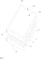
- FIG. 1 is a perspective view of a display device according to some embodiments of the present disclosure.
- a display device 100 includes an array substrate 10 and an opposite substrate 20.
- the array substrate 10 is disposed opposite to the opposite substrate 20, thereby together forming a display panel of the display device 100 and then implementing display function of the display device 100.
- the display device 100 further includes a display region 101 and a peripheral region 102 around the display region 101.
- the display region 101 is mainly used to implement the display function of the display device 100, and the peripheral region 102 is mainly used for wiring and the like.
- the array substrate 10 includes a base substrate 11, data lines 12 and gate lines 13 on the base substrate 11.
- the data lines 12 extend in a first direction on the base substrate 11, and the data lines 12 are arranged in parallel along a second direction.
- the gate lines 13 extend in the second direction on the base substrate 11, and the gate lines 13 are arranged in parallel along the first direction.
- Each pixel structure 14 includes thin film transistors 15 (shown in FIG. 2 ) which are respectively connected to the data line 12 and the gate line 13.
- the display device 100 is an OLED display device, and an OLED layer is further provided on the array substrate 10.
- the display device 100 may also be a conventional liquid crystal display device.
- FIG. 2 is a schematic diagram of the pixel structure of FIG. 1 .
- the thin film transistors 15 in each pixel structure 14 include a first thin film transistor 151 and at least one second thin film transistor 152.
- the first thin film transistor 151 is configured to control size of current of organic light-emitting elements during energizing; and the second thin film transistor 152 is configured to control on or off of the current in a circuit in which it is located.
- each pixel structure 14 there are seven second thin film transistors 152 in each pixel structure 14. In each pixel structure, except for one first thin film transistor 151, all other thin film transistors are second thin film transistors 152, which are not limited thereto. In other embodiment, other numbers of second thin film transistors may also be provided in each pixel structure.
- the first thin film transistor 151 is a driving thin film transistor
- the second thin film transistor 152 is a switch thin film transistor.
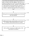
- FIG. 3 shows a method of manufacturing the array substrate of FIG. 1 ;
- FIG. 4 to FIG. 6 are partial cross-sectional views showing process of manufacturing the array substrate shown in FIG. 1 ;
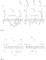
- FIG. 7 is a schematic diagram of hydrogen supplementation of a first thin film transistor and a second thin film transistor. As shown in FIG. 3 , the method includes the following steps.
- Step 301 providing a base substrate and forming a plurality of pixel structures on the base substrate; where each pixel structure includes a first thin film transistor and at least one second thin film transistor, and each of the first thin film transistor and the second thin film transistor is composed of a gate electrode, an active layer, a source electrode, a drain electrode and at least one insulating layer.
- a base substrate 11 is first provided. Then, a gate electrode 153, an active layer 154, a source electrode 155, a drain electrode 156 and at least one insulating layer 157 are formed on the base substrate 11, respectively.
- the gate electrode 153, the active layer 154, the source electrode 155, the drain electrode 156 and the at least one insulating layer 157 form the thin film transistors 15, that is, the first thin film transistor 151 and the second thin film transistor 152 as shown in FIG 4 are formed.
- the at least one insulating layer 157 includes a gate insulating layer 1571 and at least one protection layer 1572, which are not limited thereto.
- the at least one insulating layer may also include one of a gate insulating layer and at least one protection layer.
- the at least one protection layer 1572 includes a first passivation layer 1573 and a second passivation layer 1574.
- the active layer 154 is on the base substrate 11.
- the source electrode 155 and the drain electrode 156 are respectively located at two sides of the active layer 154.
- the source electrode 155 and the drain electrode 156 are in contact with two ends of the active layer 154, respectively.
- the gate insulating layer covers the active layer 154, the source electrode 155 and the drain electrode 156.
- the gate electrode 153 is disposed on the gate insulating layer 1571 and located above the active layer 154.
- the first passivation layer 1573 covers the gate electrode 153 and the gate insulating layer 1571.
- the second passivation layer 1574 is located on the first passivation layer 1573.
- the gate lines 13 may also be formed simultaneously in the process of forming the gate electrode 153.
- the data lines 12 may also be formed simultaneously in the process of forming the source electrode 155. In this way, a plurality of pixel structures is formed on the base substrate 11 with the first thin film transistor 151 and the second thin film transistor 152 in the pixel structure.
- Step 302 forming holes in at least one insulating layer of the first thin film transistor.
- holes may be formed in the first thin film transistor 151, thereby forming through holes in at least one insulating layer 157 of the thin film transistor 151 to expose the source electrode 155 and the drain electrode 156 of the first thin film transistor 151.
- a first mask 200 (as shown in FIG. 4 ) having light transmission regions 210 and opaque regions 220 may be first provided.
- the first mask is aligned with the base substrate 11, so that the light transmission regions of the first mask are respectively corresponding to the source electrode 155 and the drain electrode 156 of the first thin film transistor 151, and are respectively located above the source electrode 155 and the drain electrode 156 of the first thin film transistor 151.
- the at least one insulating layer 157 of the first thin film transistor 151 is patterned by using the first mask, thereby forming a first through hole 1581 and a second through hole 1582 in the at least one insulating layer 157, as shown in FIG. 5 .
- the first through hole 1581 is located above the source electrode 155 of the first thin film transistor 151, and the second through hole 1582 is located above the drain electrode 156 of the first thin film transistor 151, thereby exposing the source electrode 155 and the drain electrode 156 of the first thin film transistor 151 as shown in FIG. 5 .
- the first through hole 1581 and the second through hole 1582 are defined through the gate insulating layer 1571, the first passivation layer 1573 and the second passivation layer 1574 of the first thin film transistor 151, respectively, which are not limited thereto.
- there is no gate insulating layer on the source electrode and the drain electrode and only a first passivation layer and a second passivation layer are provided, that is, the at least one insulating layer includes the first passivation layer and the second passivation layer, then, it is only needed to form holes in the first passivation layer and the second passivation layer, thereby forming through holes to expose the source electrode and the drain electrode.
- Step 303 performing hydrogen supplementation on the first thin film transistor and the second thin film transistor.
- hydrogen supplementation may be performed on the first thin film transistor 151 and the second thin film transistor 152, thereby repairing internal defects of the active layer 154 of the first thin film transistor 151 and the second thin film transistor 152.
- performing hydrogen supplementation on the first thin film transistor 151 and the second thin film transistor 152 may include: placing the first thin film transistor 151 and the second thin film transistor 152 in a sealed container; then, heating the sealed container so that the temperature in the sealed container reaches a high temperature of 440 degrees to 460 degrees; maintaining the temperature in the sealed container at the high temperature of 440 degrees to 460 degrees, and continuing heating for 28 minutes to 32 minutes, thereby enabling hydrogen ions in the at least one insulating layer 157 of the first thin film transistor 151 and the second thin film transistor 152 to diffuse into the active layer 154.
- performing hydrogen supplementation on the first thin film transistor 151 and the second thin film transistor 152 includes: placing the first thin film transistor 151 and the second thin film transistor 152 in a sealed container; maintaining the temperature in the sealed container at the high temperature of 450 degrees, and continuing heating for 30 minutes, thereby enabling hydrogen ions in the at least one insulating layer 157 of the first thin film transistor 151 and the second thin film transistor 152 to diffuse into the active layer 154.
- FIG. 7 is a schematic diagram of hydrogen supplementation of a first thin film transistor and a second thin film transistor.
- hydrogen ions diffuse into the active layer 154 from the at least one insulating layer 157 of the first thin film transistor 151 and the second thin film transistor 152, along paths indicated by broken line as shown in FIG. 7 . Due to the presence of the first through hole 1581 and the second through hole 1582 in the at least one insulating layer 157 of the first thin film transistor 151, there is no hydrogen source for providing hydrogen ions to the active layer 154, at positions corresponding to the first through hole 1581 and the second through hole 1582.
- the presence of the first through hole and the second through hole is equivalent to reduction of the hydrogen source for providing hydrogen ions to the active layer 154 in the first thin film transistor 151. Since no through hole is defined in the second thin film transistor 152, the hydrogen source for providing hydrogen ions to the active layer 154 in the second thin film transistor 152 is sufficient, and more hydrogen ions can be provided to the active layer 154.
- the hydrogen source is reduced, and then the hydrogen supplementation effect of the first thin film transistor 151 is weakened. In this way, a slope of a current-voltage curve of the first thin film transistor 151 can be appropriately reduced, thereby reducing current difference caused by difference in threshold voltages.
- the hydrogen supplementation of the second thin film transistor 152 is normal, and the hydrogen supplementation effect of the second thin film transistor 152 may be considered to be enhanced as compared with the first thin film transistor 151.
- the electron mobility of the second thin film transistor 152 can be increased as much as possible, charging capacity of a capacitor can be increased, and the current difference between circuits can be reduced, so that the display device 100 can emit light uniformly, reduce probability of occurrence of Mura, and reduce the Mura effect.
- Step 304 forming holes in at least one insulating layer of the second thin film transistor.
- holes may be formed in the second thin film transistor 152, thereby forming through holes 1583, 1584 in at least one insulating layer 157 of the second thin film transistor 152 to expose the source electrode 155 and the drain electrode 156 of the second thin film transistor 152, as shown in FIG. 6 .
- a second mask 300 (as shown in FIG. 6 ) having light transmission regions 310 and opaque regions 320 may be first provided.
- the second mask is aligned with the base substrate 11, so that the light transmission regions of the second mask are respectively corresponding to the source electrode 155 and the drain electrode 156 of the second thin film transistor 152, and are respectively located above the source electrode 155 and the drain electrode 156 of the second thin film transistor 152.
- the at least one insulating layer 157 of the second thin film transistor 152 is patterned by using the second mask, thereby forming a third through hole 1583 and a fourth through hole 1584 in the at least one insulating layer 157, as shown in FIG. 6 .
- the third through hole 1583 is located above the source electrode 155 of the second thin film transistor 152, and the fourth through hole 1584 is located above the drain electrode 156 of the second thin film transistor 152, thereby exposing the source electrode 155 and the drain electrode 156 of the second thin film transistor 152 as shown in FIG. 6 .
- the third through hole 1583 and the fourth through hole 1584 are defined through the gate insulating layer 1571, the first passivation layer 1573 and the second passivation layer 1574 of the second thin film transistor 152, respectively, which are not limited thereto.
- there is no gate insulating layer on the source electrode and the drain electrode and only a first passivation layer and a second passivation layer are provided, that is, the at least one insulating layer includes the first passivation layer and the second passivation layer, then, it is only needed to form holes in the first passivation layer and the second passivation layer, thereby forming through holes to expose the source electrode and the drain electrode.
- holes are first formed above the source electrode 155 and the drain electrode 156 of the first thin film transistor 151, and then the first thin film transistor 151 and the second thin film transistor 152 are subjected to hydrogen supplementation treatment. In this way, the first thin film transistor 151 and the second thin film transistor 152 can be repaired and compensated in different degrees.
- the present disclosure is not limited thereto, and in other embodiments, holes may be respectively formed in lateral sides of the source electrode and the drain electrode of the first thin film transistor, thereby exposing the source electrode and the drain electrode from the lateral sides. Holes may also be formed in a certain area near the source electrode and the drain electrode of the first thin film transistor without exposing the source electrode and the drain electrode.
- holes may be formed in a certain area at lateral sides of the source electrode and the drain electrode, or holes may be formed above the source electrode and the drain electrode without exposing the source electrode and the drain electrode, and then the first thin film transistor and the second thin film transistor are subjected to hydrogen supplementation treatment, so that the first thin film transistor and the second thin film transistor can be repaired and compensated in different degrees.
- an array substrate 10 includes a base substrate 11 and a plurality of pixel structures 14 disposed on the base substrate 11.
- Each pixel structure 14 includes a driving thin film transistor 151 and at least one switch thin film transistor 152.
- a hydrogen ion concentration in an active layer 154 of the driving thin film transistor is lower than a hydrogen ion concentration in an active layer 154 of the at least one switch thin film transistor.
- One embodiment of the present disclosure further provides a display device including the above array substrate 10.
- a base substrate is provided and a plurality of pixel structures is formed on the base substrate.
- Each pixel structure includes a first thin film transistor and at least one second thin film transistor, and each of the first thin film transistor and the second thin film transistor is composed of a gate electrode, an active layer, a source electrode, a drain electrode and at least one insulating layer. Then, holes are formed in at least one insulating layer of the first thin film transistor, and hydrogen supplementation is performed on the first thin film transistor and the second thin film transistor. And then, holes are formed in at least one insulating layer of the second thin film transistor.
- the first thin film transistor and the second thin film transistor can be repaired and compensated in different degrees by hydrogen supplementation. Since the first thin film transistor 151 is provided with through holes, the hydrogen supplementation effect of the first thin film transistor is weakened. In this way, a slope of a current-voltage curve of the first thin film transistor can be appropriately reduced, thereby reducing current difference caused by difference in threshold voltages.
- the electron mobility of the second thin film transistor can be increased as much as possible, charging capacity of a capacitor can be increased, and the current difference between circuits can be reduced, so that the display device can emit light uniformly, reduce probability of occurrence of Mura, and reduce the Mura effect.
Landscapes
- Engineering & Computer Science (AREA)
- Microelectronics & Electronic Packaging (AREA)
- Physics & Mathematics (AREA)
- Geometry (AREA)
- Devices For Indicating Variable Information By Combining Individual Elements (AREA)
- Electroluminescent Light Sources (AREA)
- Chemical & Material Sciences (AREA)
- Crystallography & Structural Chemistry (AREA)
- Liquid Crystal (AREA)
Abstract
Description
- This application claims the benefit and priority of Chinese Application No.
201810004387.6, filed on January 3, 2018 - The present disclosure relates to the field of display technologies, and in particular to a method for manufacturing an array substrate, an array substrate, and a display device.
- Due to the rise of the global information society and the development of technologies, display technologies are changing rapidly and there are more and more kinds of display technologies, such as the liquid crystal display technology, the organic light-emitting diode (OLED) display technology and the electrophoretic display technology. Comparing with other kinds of display devices, OLED display devices have advantages of self-luminous display, fast response, high brightness and wide viewing angle, and thus have wide application prospects. However, the OLED display device has disadvantages such as uneven illumination and presence of light and dark mura at different positions.
- One embodiment of the present disclosure provides a method of manufacturing an array substrate, including:
- forming a plurality of pixel structures on a base substrate; wherein at least one of the plurality of pixel structures includes a first thin film transistor having at least one insulating layer and at least one second thin film transistor having at least one insulating layer;
- forming holes in the at least one insulating layer of the first thin film transistor;
- performing hydrogen supplementation on the first thin film transistor and the at least one second thin film transistor; and
- forming holes in the at least one insulating layer of the at least one second thin film transistor.
- One embodiment of the present disclosure further provides an array substrate which is manufactured by the above method.
- One embodiment of the present disclosure further provides a display device including the above array substrate.
- One embodiment of the present disclosure further provides an array substrate including: a base substrate; and a plurality of pixel structures on the base substrate. Each of the plurality of pixel structures includes a driving thin film transistor and at least one switch thin film transistor. A hydrogen ion concentration in an active layer of the driving thin film transistor is lower than a hydrogen ion concentration in an active layer of the at least one switch thin film transistor.
- One embodiment of the present disclosure further provides a display device including the above array substrate.
- In order to illustrate technical solutions according to embodiments of the present disclosure more clearly, drawings to be used in the description of the embodiments will be described briefly hereinafter. Apparently, the drawings described hereinafter are only some embodiments of the present disclosure, and other drawings may be obtained by those skilled in the art according to those drawings without creative work.
-
FIG. 1 is a perspective view of a display device according to some embodiments of the present disclosure; -
FIG. 2 is a schematic view showing a pixel structure of the display device ofFIG. 1 ; -
FIG. 3 is a flowchart of a method of manufacturing an array substrate of the display device ofFIG. 1 ; -
FIG. 4 to FIG. 6 are partial cross-sectional views showing process of manufacturing an array substrate of the display device shown inFIG. 1 ; and -
FIG. 7 is a schematic diagram of hydrogen supplementation of a first thin film transistor and a second thin film transistor. - The technical solution of embodiments of the present disclosure will be described hereinafter in a clear and complete manner in conjunction with the drawings and embodiments. Obviously, the following embodiments are merely a part of, rather than all of, the embodiments of the present disclosure, and based on these embodiments, a person skilled in the art may obtain the other embodiments, which also fall within the scope of the present disclosure.
- Although the OLED display technology has many advantages, in the OLED display device, there are certain defect differences in the low-temperature polysilicon due to more or less grain boundaries in the low-temperature polysilicon, resulting in insufficient structural uniformity of the active layer. Thus, it is necessary to use hydrogenation process to perform hydrogen supplementation on the active layer. However, simply performing hydrogen supplementation treatment on thin film transistors on the array substrate will increase differences in driving current, resulting in uneven light emission of the OLED display device with light and dark mura appearing at different positions.
- In view of this, one embodiment of the present disclosure provides a method for manufacturing an array substrate, an array substrate and a display device, which can solve the problem of uneven light emission of the OLED display device with light and dark mura appearing at different positions.
- Referring to
FIG. 1, FIG. 1 is a perspective view of a display device according to some embodiments of the present disclosure. As shown inFIG. 1 , adisplay device 100 includes anarray substrate 10 and anopposite substrate 20. Thearray substrate 10 is disposed opposite to theopposite substrate 20, thereby together forming a display panel of thedisplay device 100 and then implementing display function of thedisplay device 100. Thedisplay device 100 further includes adisplay region 101 and aperipheral region 102 around thedisplay region 101. Thedisplay region 101 is mainly used to implement the display function of thedisplay device 100, and theperipheral region 102 is mainly used for wiring and the like. - The
array substrate 10 includes abase substrate 11,data lines 12 andgate lines 13 on thebase substrate 11. Thedata lines 12 extend in a first direction on thebase substrate 11, and thedata lines 12 are arranged in parallel along a second direction. Thegate lines 13 extend in the second direction on thebase substrate 11, and thegate lines 13 are arranged in parallel along the first direction. - An orthographic projection of the
data lines 12 on thebase substrate 11 and an orthographic projection of thegate lines 13 on thebase substrate 11 cross each other and define an array ofpixel structures 14 in thedisplay region 101 of thedisplay device 100. Eachpixel structure 14 includes thin film transistors 15 (shown inFIG. 2 ) which are respectively connected to thedata line 12 and thegate line 13. - In one embodiment, the
display device 100 is an OLED display device, and an OLED layer is further provided on thearray substrate 10. However, it is not limited thereto, in other embodiment, thedisplay device 100 may also be a conventional liquid crystal display device. - Referring also to
FIG. 2, FIG. 2 is a schematic diagram of the pixel structure ofFIG. 1 . As shown inFIG. 2 , thethin film transistors 15 in eachpixel structure 14 include a firstthin film transistor 151 and at least one secondthin film transistor 152. The firstthin film transistor 151 is configured to control size of current of organic light-emitting elements during energizing; and the secondthin film transistor 152 is configured to control on or off of the current in a circuit in which it is located. - In one embodiment, there are seven second
thin film transistors 152 in eachpixel structure 14. In each pixel structure, except for one firstthin film transistor 151, all other thin film transistors are secondthin film transistors 152, which are not limited thereto. In other embodiment, other numbers of second thin film transistors may also be provided in each pixel structure. - Optionally, the first
thin film transistor 151 is a driving thin film transistor, and the secondthin film transistor 152 is a switch thin film transistor. - Referring to
FIG. 3 to FIG. 7 ,FIG. 3 shows a method of manufacturing the array substrate ofFIG. 1 ;FIG. 4 to FIG. 6 are partial cross-sectional views showing process of manufacturing the array substrate shown inFIG. 1 ; andFIG. 7 is a schematic diagram of hydrogen supplementation of a first thin film transistor and a second thin film transistor. As shown inFIG. 3 , the method includes the following steps. - Step 301: providing a base substrate and forming a plurality of pixel structures on the base substrate; where each pixel structure includes a first thin film transistor and at least one second thin film transistor, and each of the first thin film transistor and the second thin film transistor is composed of a gate electrode, an active layer, a source electrode, a drain electrode and at least one insulating layer.
- In this step, a
base substrate 11 is first provided. Then, agate electrode 153, anactive layer 154, asource electrode 155, adrain electrode 156 and at least oneinsulating layer 157 are formed on thebase substrate 11, respectively. Thegate electrode 153, theactive layer 154, thesource electrode 155, thedrain electrode 156 and the at least oneinsulating layer 157 form thethin film transistors 15, that is, the firstthin film transistor 151 and the secondthin film transistor 152 as shown inFIG 4 are formed. - Optionally, in one embodiment, the at least one
insulating layer 157 includes agate insulating layer 1571 and at least oneprotection layer 1572, which are not limited thereto. In other embodiment, the at least one insulating layer may also include one of a gate insulating layer and at least one protection layer. - In one embodiment, the at least one
protection layer 1572 includes afirst passivation layer 1573 and asecond passivation layer 1574. - In one embodiment, the
active layer 154 is on thebase substrate 11. Thesource electrode 155 and thedrain electrode 156 are respectively located at two sides of theactive layer 154. Thesource electrode 155 and thedrain electrode 156 are in contact with two ends of theactive layer 154, respectively. The gate insulating layer covers theactive layer 154, thesource electrode 155 and thedrain electrode 156. Thegate electrode 153 is disposed on thegate insulating layer 1571 and located above theactive layer 154. Thefirst passivation layer 1573 covers thegate electrode 153 and thegate insulating layer 1571. Thesecond passivation layer 1574 is located on thefirst passivation layer 1573. - The gate lines 13 (shown in
FIG. 1 ) may also be formed simultaneously in the process of forming thegate electrode 153. The data lines 12 (shown inFIG. 1 ) may also be formed simultaneously in the process of forming thesource electrode 155. In this way, a plurality of pixel structures is formed on thebase substrate 11 with the firstthin film transistor 151 and the secondthin film transistor 152 in the pixel structure. - Step 302: forming holes in at least one insulating layer of the first thin film transistor.
- In this step, after the first
thin film transistor 151 and the secondthin film transistor 152 are formed on thebase substrate 11, holes may be formed in the firstthin film transistor 151, thereby forming through holes in at least one insulatinglayer 157 of thethin film transistor 151 to expose thesource electrode 155 and thedrain electrode 156 of the firstthin film transistor 151. - Specifically, a first mask 200 (as shown in
FIG. 4 ) havinglight transmission regions 210 andopaque regions 220 may be first provided. The first mask is aligned with thebase substrate 11, so that the light transmission regions of the first mask are respectively corresponding to thesource electrode 155 and thedrain electrode 156 of the firstthin film transistor 151, and are respectively located above thesource electrode 155 and thedrain electrode 156 of the firstthin film transistor 151. Then, the at least one insulatinglayer 157 of the firstthin film transistor 151 is patterned by using the first mask, thereby forming a first throughhole 1581 and a second throughhole 1582 in the at least one insulatinglayer 157, as shown inFIG. 5 . The first throughhole 1581 is located above thesource electrode 155 of the firstthin film transistor 151, and the second throughhole 1582 is located above thedrain electrode 156 of the firstthin film transistor 151, thereby exposing thesource electrode 155 and thedrain electrode 156 of the firstthin film transistor 151 as shown inFIG. 5 . - In one embodiment, the first through
hole 1581 and the second throughhole 1582 are defined through thegate insulating layer 1571, thefirst passivation layer 1573 and thesecond passivation layer 1574 of the firstthin film transistor 151, respectively, which are not limited thereto. In other embodiments, for example, in a bottom-gate type thin film transistor, there is no gate insulating layer on the source electrode and the drain electrode, and only a first passivation layer and a second passivation layer are provided, that is, the at least one insulating layer includes the first passivation layer and the second passivation layer, then, it is only needed to form holes in the first passivation layer and the second passivation layer, thereby forming through holes to expose the source electrode and the drain electrode. - Step 303: performing hydrogen supplementation on the first thin film transistor and the second thin film transistor.
- In this step, after the first through
hole 1581 and the second throughhole 1582 are formed in the firstthin film transistor 151, hydrogen supplementation may be performed on the firstthin film transistor 151 and the secondthin film transistor 152, thereby repairing internal defects of theactive layer 154 of the firstthin film transistor 151 and the secondthin film transistor 152. - Specifically, performing hydrogen supplementation on the first
thin film transistor 151 and the secondthin film transistor 152 may include: placing the firstthin film transistor 151 and the secondthin film transistor 152 in a sealed container; then, heating the sealed container so that the temperature in the sealed container reaches a high temperature of 440 degrees to 460 degrees; maintaining the temperature in the sealed container at the high temperature of 440 degrees to 460 degrees, and continuing heating for 28 minutes to 32 minutes, thereby enabling hydrogen ions in the at least one insulatinglayer 157 of the firstthin film transistor 151 and the secondthin film transistor 152 to diffuse into theactive layer 154. - In one embodiment, performing hydrogen supplementation on the first
thin film transistor 151 and the secondthin film transistor 152 includes: placing the firstthin film transistor 151 and the secondthin film transistor 152 in a sealed container; maintaining the temperature in the sealed container at the high temperature of 450 degrees, and continuing heating for 30 minutes, thereby enabling hydrogen ions in the at least one insulatinglayer 157 of the firstthin film transistor 151 and the secondthin film transistor 152 to diffuse into theactive layer 154. - Referring to
FIG. 7, FIG. 7 is a schematic diagram of hydrogen supplementation of a first thin film transistor and a second thin film transistor. As shown inFIG. 7 , when performing hydrogen supplementation on the firstthin film transistor 151 and the secondthin film transistor 152, hydrogen ions diffuse into theactive layer 154 from the at least one insulatinglayer 157 of the firstthin film transistor 151 and the secondthin film transistor 152, along paths indicated by broken line as shown inFIG. 7 . Due to the presence of the first throughhole 1581 and the second throughhole 1582 in the at least one insulatinglayer 157 of the firstthin film transistor 151, there is no hydrogen source for providing hydrogen ions to theactive layer 154, at positions corresponding to the first throughhole 1581 and the second throughhole 1582. Thus, the presence of the first through hole and the second through hole is equivalent to reduction of the hydrogen source for providing hydrogen ions to theactive layer 154 in the firstthin film transistor 151. Since no through hole is defined in the secondthin film transistor 152, the hydrogen source for providing hydrogen ions to theactive layer 154 in the secondthin film transistor 152 is sufficient, and more hydrogen ions can be provided to theactive layer 154. - In contrast, since the first
thin film transistor 151 is provided with through holes, the hydrogen source is reduced, and then the hydrogen supplementation effect of the firstthin film transistor 151 is weakened. In this way, a slope of a current-voltage curve of the firstthin film transistor 151 can be appropriately reduced, thereby reducing current difference caused by difference in threshold voltages. The hydrogen supplementation of the secondthin film transistor 152 is normal, and the hydrogen supplementation effect of the secondthin film transistor 152 may be considered to be enhanced as compared with the firstthin film transistor 151. In this way, the electron mobility of the secondthin film transistor 152 can be increased as much as possible, charging capacity of a capacitor can be increased, and the current difference between circuits can be reduced, so that thedisplay device 100 can emit light uniformly, reduce probability of occurrence of Mura, and reduce the Mura effect. - Step 304: forming holes in at least one insulating layer of the second thin film transistor.
- In this step, after performing hydrogen supplementation on the first
thin film transistor 151 and the secondthin film transistor 152, holes may be formed in the secondthin film transistor 152, thereby forming throughholes layer 157 of the secondthin film transistor 152 to expose thesource electrode 155 and thedrain electrode 156 of the secondthin film transistor 152, as shown inFIG. 6 . - Specifically, a second mask 300 (as shown in
FIG. 6 ) havinglight transmission regions 310 andopaque regions 320 may be first provided. The second mask is aligned with thebase substrate 11, so that the light transmission regions of the second mask are respectively corresponding to thesource electrode 155 and thedrain electrode 156 of the secondthin film transistor 152, and are respectively located above thesource electrode 155 and thedrain electrode 156 of the secondthin film transistor 152. Then, the at least one insulatinglayer 157 of the secondthin film transistor 152 is patterned by using the second mask, thereby forming a third throughhole 1583 and a fourth throughhole 1584 in the at least one insulatinglayer 157, as shown inFIG. 6 . The third throughhole 1583 is located above thesource electrode 155 of the secondthin film transistor 152, and the fourth throughhole 1584 is located above thedrain electrode 156 of the secondthin film transistor 152, thereby exposing thesource electrode 155 and thedrain electrode 156 of the secondthin film transistor 152 as shown inFIG. 6 . - In one embodiment, the third through
hole 1583 and the fourth throughhole 1584 are defined through thegate insulating layer 1571, thefirst passivation layer 1573 and thesecond passivation layer 1574 of the secondthin film transistor 152, respectively, which are not limited thereto. In other embodiments, for example, in a bottom-gate type thin film transistor, there is no gate insulating layer on the source electrode and the drain electrode, and only a first passivation layer and a second passivation layer are provided, that is, the at least one insulating layer includes the first passivation layer and the second passivation layer, then, it is only needed to form holes in the first passivation layer and the second passivation layer, thereby forming through holes to expose the source electrode and the drain electrode. - In one embodiment, holes are first formed above the
source electrode 155 and thedrain electrode 156 of the firstthin film transistor 151, and then the firstthin film transistor 151 and the secondthin film transistor 152 are subjected to hydrogen supplementation treatment. In this way, the firstthin film transistor 151 and the secondthin film transistor 152 can be repaired and compensated in different degrees. The present disclosure is not limited thereto, and in other embodiments, holes may be respectively formed in lateral sides of the source electrode and the drain electrode of the first thin film transistor, thereby exposing the source electrode and the drain electrode from the lateral sides. Holes may also be formed in a certain area near the source electrode and the drain electrode of the first thin film transistor without exposing the source electrode and the drain electrode. For example, holes may be formed in a certain area at lateral sides of the source electrode and the drain electrode, or holes may be formed above the source electrode and the drain electrode without exposing the source electrode and the drain electrode, and then the first thin film transistor and the second thin film transistor are subjected to hydrogen supplementation treatment, so that the first thin film transistor and the second thin film transistor can be repaired and compensated in different degrees. - One embodiment of the present disclosure further provides an array substrate. As shown in
FIG. 1 andFIG. 4 toFIG. 6 , anarray substrate 10 includes abase substrate 11 and a plurality ofpixel structures 14 disposed on thebase substrate 11. Eachpixel structure 14 includes a drivingthin film transistor 151 and at least one switchthin film transistor 152. A hydrogen ion concentration in anactive layer 154 of the driving thin film transistor is lower than a hydrogen ion concentration in anactive layer 154 of the at least one switch thin film transistor. - One embodiment of the present disclosure further provides a display device including the
above array substrate 10. - In the method for manufacturing an array substrate, the array substrate, and the display device provided in the embodiments of the present disclosure, a base substrate is provided and a plurality of pixel structures is formed on the base substrate. Each pixel structure includes a first thin film transistor and at least one second thin film transistor, and each of the first thin film transistor and the second thin film transistor is composed of a gate electrode, an active layer, a source electrode, a drain electrode and at least one insulating layer. Then, holes are formed in at least one insulating layer of the first thin film transistor, and hydrogen supplementation is performed on the first thin film transistor and the second thin film transistor. And then, holes are formed in at least one insulating layer of the second thin film transistor. In this way, by first forming holes in the first thin film transistor, then simultaneously performing hydrogen supplementation on the first thin film transistor and the second thin film transistor, and then forming holes in the second thin film transistor, the first thin film transistor and the second thin film transistor can be repaired and compensated in different degrees by hydrogen supplementation. Since the first
thin film transistor 151 is provided with through holes, the hydrogen supplementation effect of the first thin film transistor is weakened. In this way, a slope of a current-voltage curve of the first thin film transistor can be appropriately reduced, thereby reducing current difference caused by difference in threshold voltages. Meanwhile, the electron mobility of the second thin film transistor can be increased as much as possible, charging capacity of a capacitor can be increased, and the current difference between circuits can be reduced, so that the display device can emit light uniformly, reduce probability of occurrence of Mura, and reduce the Mura effect. - The above are merely the preferred embodiments of the present disclosure and shall not be used to limit the scope of the present disclosure. It should be noted that, a person skilled in the art may make improvements and modifications without departing from the principle of the present disclosure, and these improvements and modifications shall also fall within the scope of the present disclosure. Therefore, the protection scope of the present disclosure should be determined by the scope of the claims.
Claims (12)
- A method of manufacturing an array substrate, comprising:forming a plurality of pixel structures on a base substrate; wherein at least one of the plurality of pixel structures includes a first thin film transistor having at least one insulating layer and at least one second thin film transistor having at least one insulating layer;forming holes in the at least one insulating layer of the first thin film transistor;performing hydrogen supplementation on the first thin film transistor and the at least one second thin film transistor; andforming holes in the at least one insulating layer of the at least one second thin film transistor.
- The method according to claim 1, wherein each of the first thin film transistor and the at least one second thin film transistor further includes a gate electrode, an active layer, a source electrode and a drain electrode, respectively.
- The method according to claim 2, wherein the forming holes in the at least one insulating layer of the first thin film transistor, includes:aligning a first mask with the base substrate;patterning the at least one insulating layer of the first thin film transistor by using the first mask, thereby forming a first through hole and a second through hole in the at least one insulating layer of the first thin film transistor to expose the source electrode and the drain electrode of the first thin film transistor, respectively.
- The method according to claim 3, wherein the forming holes in the at least one insulating layer of the at least one second thin film transistor, includes:aligning a second mask with the base substrate;patterning the at least one insulating layer of the at least one second thin film transistor by using the second mask, thereby forming a third through hole and a fourth through hole in the at least one insulating layer of the at least one second thin film transistor to expose the source electrode and the drain electrode of the at least one second thin film transistor, respectively.
- The method according to claim 2, wherein the performing hydrogen supplementation on the first thin film transistor and the at least one second thin film transistor, includes:
placing the first thin film transistor and the at least one second thin film transistor in a sealed container with a temperature of 440 degrees to 460 degrees, and continuously heating for 28 minutes to 32 minutes, thereby enabling some hydrogen ions in the at least one insulating layer of the first thin film transistor to diffuse into the active layer of the first thin film transistor, and enabling some hydrogen ions in the at least one insulating layer of the at least one second thin film transistor to diffuse into the active layer of the at least one second thin film transistor. - The method according to claim 5, wherein the performing hydrogen supplementation on the first thin film transistor and the at least one second thin film transistor, includes:
placing the first thin film transistor and the at least one second thin film transistor in the sealed container with a temperature of 450 degrees, and continuously heating for 30 minutes, thereby enabling some hydrogen ions in the at least one insulating layer of the first thin film transistor to diffuse into the active layer of the first thin film transistor, and enabling some hydrogen ions in the at least one insulating layer of the at least one second thin film transistor to diffuse into the active layer of the at least one second thin film transistor. - The method according to claim 2, wherein the at least one insulating layer of the first thin film transistor includes a gate insulating layer and/or at least one protection layer; the at least one insulating layer of the at least one second thin film transistor includes a gate insulating layer and/or at least one protection layer.
- The method according to any one of claims 1 to 7, wherein the first thin film transistor is a driving thin film transistor, and the at least one second thin film transistor is a switch thin film transistor.
- An array substrate, wherein the array substrate is manufactured by the method according to any one of claims 1 to 8.
- A display device comprising the array substrate according to claim 9.
- An array substrate comprising:a base substrate; anda plurality of pixel structures on the base substrate;wherein each of the plurality of pixel structures includes a driving thin film transistor and at least one switch thin film transistor; a hydrogen ion concentration in an active layer of the driving thin film transistor is lower than a hydrogen ion concentration in an active layer of the at least one switch thin film transistor.
- A display device comprising the array substrate according to claim 11.
Applications Claiming Priority (2)
| Application Number | Priority Date | Filing Date | Title |
|---|---|---|---|
| CN201810004387.6A CN109994510B (en) | 2018-01-03 | 2018-01-03 | Method for manufacturing an array substrate, array substrate and display device |
| PCT/CN2018/108324 WO2019134409A1 (en) | 2018-01-03 | 2018-09-28 | Manufacturing method for array substrate, array substrate and display device |
Publications (2)
| Publication Number | Publication Date |
|---|---|
| EP3736870A1 true EP3736870A1 (en) | 2020-11-11 |
| EP3736870A4 EP3736870A4 (en) | 2021-09-29 |
Family
ID=67128543
Family Applications (1)
| Application Number | Title | Priority Date | Filing Date |
|---|---|---|---|
| EP18898178.1A Withdrawn EP3736870A4 (en) | 2018-01-03 | 2018-09-28 | METHOD OF MANUFACTURING NETWORK SUBSTRATE, NETWORK SUBSTRATE AND DISPLAY DEVICE |
Country Status (4)
| Country | Link |
|---|---|
| US (1) | US11508763B2 (en) |
| EP (1) | EP3736870A4 (en) |
| CN (1) | CN109994510B (en) |
| WO (1) | WO2019134409A1 (en) |
Cited By (1)
| Publication number | Priority date | Publication date | Assignee | Title |
|---|---|---|---|---|
| EP4086888A3 (en) * | 2021-05-06 | 2023-01-25 | Samsung Display Co., Ltd. | Light emitting display device |
Families Citing this family (4)
| Publication number | Priority date | Publication date | Assignee | Title |
|---|---|---|---|---|
| CN110828486B (en) * | 2019-11-19 | 2023-05-12 | 云谷(固安)科技有限公司 | Manufacturing method of display panel and display panel |
| CN112366210B (en) * | 2020-11-25 | 2025-01-14 | 厦门天马微电子有限公司 | Array substrate and manufacturing method thereof, display panel and device |
| CN113488486B (en) * | 2021-06-29 | 2024-06-28 | 昆山工研院新型平板显示技术中心有限公司 | Method for manufacturing array substrate and array substrate |
| CN113745245B (en) * | 2021-08-16 | 2022-12-23 | 武汉华星光电半导体显示技术有限公司 | Display panel, manufacturing method thereof and mobile terminal |
Family Cites Families (14)
| Publication number | Priority date | Publication date | Assignee | Title |
|---|---|---|---|---|
| TW200500979A (en) * | 2003-05-20 | 2005-01-01 | Adv Lcd Tech Dev Ct Co Ltd | Light emission type display apparatus |
| KR100656497B1 (en) * | 2004-02-09 | 2006-12-11 | 삼성에스디아이 주식회사 | Organic light emitting display device and manufacturing method |
| CN103022355B (en) * | 2012-12-21 | 2016-04-06 | 昆山工研院新型平板显示技术中心有限公司 | A kind of low-temperature polysilicon film transistor and preparation method thereof |
| CN103456765B (en) | 2013-09-10 | 2015-09-16 | 深圳市华星光电技术有限公司 | Active organic electroluminescence device backboard and preparation method thereof |
| US9425217B2 (en) * | 2013-09-23 | 2016-08-23 | Semiconductor Energy Laboratory Co., Ltd. | Semiconductor device |
| KR102328678B1 (en) * | 2015-02-09 | 2021-11-19 | 삼성디스플레이 주식회사 | Thin film transistor substrate, display apparatus comprising the same, method for manufacturing thin film transistor substrate, and method for manufacturing display apparatus |
| KR102304726B1 (en) * | 2015-03-27 | 2021-09-27 | 삼성디스플레이 주식회사 | Manufacturing method of display device and display device thereof |
| KR20160122893A (en) * | 2015-04-14 | 2016-10-25 | 삼성디스플레이 주식회사 | Thin film transistor substrate, display apparatus comprising the same, method for manufacturing thin film transistor substrate, and method for manufacturing display apparatus |
| CN105185788A (en) | 2015-09-01 | 2015-12-23 | 武汉华星光电技术有限公司 | Array substrate and fabrication method thereof |
| CN105632905B (en) | 2016-01-21 | 2018-05-11 | 武汉华星光电技术有限公司 | Low-temperature polysilicon film transistor unit and preparation method thereof |
| KR102716494B1 (en) | 2016-03-18 | 2024-10-14 | 삼성디스플레이 주식회사 | Thin film transistor substrate, display device comprising the same, and method for manufacturing thin film transistor substrate |
| US10109650B2 (en) | 2016-04-01 | 2018-10-23 | Joled Inc. | Semiconductor device and active matrix substrate using semiconductor device |
| CN106384727A (en) * | 2016-09-30 | 2017-02-08 | 昆山国显光电有限公司 | Thin-film transistor device preparation method and thin-film transistor device |
| CN107818989B (en) * | 2017-10-20 | 2020-08-04 | 武汉华星光电技术有限公司 | Array substrate and method of making the same |
-
2018
- 2018-01-03 CN CN201810004387.6A patent/CN109994510B/en active Active
- 2018-09-28 US US16/760,009 patent/US11508763B2/en active Active
- 2018-09-28 EP EP18898178.1A patent/EP3736870A4/en not_active Withdrawn
- 2018-09-28 WO PCT/CN2018/108324 patent/WO2019134409A1/en not_active Ceased
Cited By (2)
| Publication number | Priority date | Publication date | Assignee | Title |
|---|---|---|---|---|
| EP4086888A3 (en) * | 2021-05-06 | 2023-01-25 | Samsung Display Co., Ltd. | Light emitting display device |
| US12080724B2 (en) | 2021-05-06 | 2024-09-03 | Samsung Display Co., Ltd. | Light emitting display device |
Also Published As
| Publication number | Publication date |
|---|---|
| US11508763B2 (en) | 2022-11-22 |
| US20200350340A1 (en) | 2020-11-05 |
| WO2019134409A1 (en) | 2019-07-11 |
| EP3736870A4 (en) | 2021-09-29 |
| CN109994510B (en) | 2021-01-22 |
| CN109994510A (en) | 2019-07-09 |
Similar Documents
| Publication | Publication Date | Title |
|---|---|---|
| US20220310735A1 (en) | Display device | |
| US11508763B2 (en) | Method for manufacturing array substrate, array substrate and display device | |
| US10367073B2 (en) | Thin film transistor (TFT) with structured gate insulator | |
| US11355519B2 (en) | Array substrate, manufacturing method thereof, and display device | |
| KR102465559B1 (en) | Thin Film Transistor Substrate And Display Using The Same | |
| US20090114918A1 (en) | Panel structure and manufacturing method thereof | |
| US20220310850A1 (en) | Thin film transistor and manufacturing method thereof and electronic device | |
| US20180294286A1 (en) | Display device | |
| US9905588B2 (en) | Organic light emitting display panel and method of manufacturing the same | |
| CN108807421B (en) | Manufacturing method of TFT array substrate and TFT array substrate | |
| US10409115B2 (en) | Liquid crystal display panel, array substrate and manufacturing method thereof | |
| US10018906B2 (en) | Display device and method of manufacturing the same | |
| US20170294544A1 (en) | Thin film transistor and method thereof, array substrate, and display apparatus | |
| US9570482B2 (en) | Manufacturing method and manufacturing equipment of thin film transistor substrate | |
| US9823531B2 (en) | Thin film transistor array panel, manufacturing method thereof, and display device including the thin film transistor array panel | |
| CN104465509B (en) | A kind of OLED display device array base palte and preparation method thereof | |
| KR102449066B1 (en) | Array substrate for display device and manufacturing method thereof | |
| JP2010062173A (en) | Thin film transistor, manufacturing method thereof, electro-optic device, manufacturing method thereof and electronic apparatus | |
| US8228266B2 (en) | Active-matrix organic electroluminescent device and method for fabricating the same | |
| US9035315B2 (en) | Semiconductor device, display device, and method for manufacturing semiconductor device | |
| US9496294B2 (en) | Array substrate, manufacturing method and display device | |
| KR102235421B1 (en) | Array substrate and method of fabricating the same | |
| US20190244824A1 (en) | Array substrate, method for fabricating the same, display panel and method for fabricating the same | |
| US20080054267A1 (en) | Display apparatus and manufacturing method of the same | |
| KR20200105458A (en) | Display device and method of manufacturing display device using the same |
Legal Events
| Date | Code | Title | Description |
|---|---|---|---|
| STAA | Information on the status of an ep patent application or granted ep patent |
Free format text: STATUS: THE INTERNATIONAL PUBLICATION HAS BEEN MADE |
|
| PUAI | Public reference made under article 153(3) epc to a published international application that has entered the european phase |
Free format text: ORIGINAL CODE: 0009012 |
|
| STAA | Information on the status of an ep patent application or granted ep patent |
Free format text: STATUS: REQUEST FOR EXAMINATION WAS MADE |
|
| 17P | Request for examination filed |
Effective date: 20200610 |
|
| AK | Designated contracting states |
Kind code of ref document: A1 Designated state(s): AL AT BE BG CH CY CZ DE DK EE ES FI FR GB GR HR HU IE IS IT LI LT LU LV MC MK MT NL NO PL PT RO RS SE SI SK SM TR |
|
| AX | Request for extension of the european patent |
Extension state: BA ME |
|
| DAV | Request for validation of the european patent (deleted) | ||
| DAX | Request for extension of the european patent (deleted) | ||
| A4 | Supplementary search report drawn up and despatched |
Effective date: 20210826 |
|
| RIC1 | Information provided on ipc code assigned before grant |
Ipc: H01L 27/32 20060101ALI20210820BHEP Ipc: H01L 27/12 20060101ALI20210820BHEP Ipc: H01L 51/05 20060101AFI20210820BHEP |
|
| STAA | Information on the status of an ep patent application or granted ep patent |
Free format text: STATUS: EXAMINATION IS IN PROGRESS |
|
| 17Q | First examination report despatched |
Effective date: 20240522 |
|
| STAA | Information on the status of an ep patent application or granted ep patent |
Free format text: STATUS: THE APPLICATION HAS BEEN WITHDRAWN |
|
| 18W | Application withdrawn |
Effective date: 20241018 |