EP3736857A1 - Through hole side wettable flank - Google Patents
Through hole side wettable flank Download PDFInfo
- Publication number
- EP3736857A1 EP3736857A1 EP19172982.1A EP19172982A EP3736857A1 EP 3736857 A1 EP3736857 A1 EP 3736857A1 EP 19172982 A EP19172982 A EP 19172982A EP 3736857 A1 EP3736857 A1 EP 3736857A1
- Authority
- EP
- European Patent Office
- Prior art keywords
- lead
- wettable
- flank
- end portion
- semiconductor device
- Prior art date
- Legal status (The legal status is an assumption and is not a legal conclusion. Google has not performed a legal analysis and makes no representation as to the accuracy of the status listed.)
- Withdrawn
Links
Images




Classifications
-
- H—ELECTRICITY
- H10—SEMICONDUCTOR DEVICES; ELECTRIC SOLID-STATE DEVICES NOT OTHERWISE PROVIDED FOR
- H10W—GENERIC PACKAGES, INTERCONNECTIONS, CONNECTORS OR OTHER CONSTRUCTIONAL DETAILS OF DEVICES COVERED BY CLASS H10
- H10W70/00—Package substrates; Interposers; Redistribution layers [RDL]
- H10W70/40—Leadframes
- H10W70/421—Shapes or dispositions
-
- H—ELECTRICITY
- H10—SEMICONDUCTOR DEVICES; ELECTRIC SOLID-STATE DEVICES NOT OTHERWISE PROVIDED FOR
- H10W—GENERIC PACKAGES, INTERCONNECTIONS, CONNECTORS OR OTHER CONSTRUCTIONAL DETAILS OF DEVICES COVERED BY CLASS H10
- H10W70/00—Package substrates; Interposers; Redistribution layers [RDL]
- H10W70/40—Leadframes
- H10W70/421—Shapes or dispositions
- H10W70/438—Shapes or dispositions of side rails, e.g. having holes
-
- H—ELECTRICITY
- H10—SEMICONDUCTOR DEVICES; ELECTRIC SOLID-STATE DEVICES NOT OTHERWISE PROVIDED FOR
- H10W—GENERIC PACKAGES, INTERCONNECTIONS, CONNECTORS OR OTHER CONSTRUCTIONAL DETAILS OF DEVICES COVERED BY CLASS H10
- H10W70/00—Package substrates; Interposers; Redistribution layers [RDL]
- H10W70/40—Leadframes
- H10W70/464—Additional interconnections in combination with leadframes
- H10W70/467—Multilayered additional interconnections
-
- H—ELECTRICITY
- H10—SEMICONDUCTOR DEVICES; ELECTRIC SOLID-STATE DEVICES NOT OTHERWISE PROVIDED FOR
- H10W—GENERIC PACKAGES, INTERCONNECTIONS, CONNECTORS OR OTHER CONSTRUCTIONAL DETAILS OF DEVICES COVERED BY CLASS H10
- H10W72/00—Interconnections or connectors in packages
- H10W72/01—Manufacture or treatment
- H10W72/0198—Manufacture or treatment batch processes
-
- H—ELECTRICITY
- H10—SEMICONDUCTOR DEVICES; ELECTRIC SOLID-STATE DEVICES NOT OTHERWISE PROVIDED FOR
- H10W—GENERIC PACKAGES, INTERCONNECTIONS, CONNECTORS OR OTHER CONSTRUCTIONAL DETAILS OF DEVICES COVERED BY CLASS H10
- H10W72/00—Interconnections or connectors in packages
- H10W72/071—Connecting or disconnecting
- H10W72/075—Connecting or disconnecting of bond wires
-
- H—ELECTRICITY
- H10—SEMICONDUCTOR DEVICES; ELECTRIC SOLID-STATE DEVICES NOT OTHERWISE PROVIDED FOR
- H10W—GENERIC PACKAGES, INTERCONNECTIONS, CONNECTORS OR OTHER CONSTRUCTIONAL DETAILS OF DEVICES COVERED BY CLASS H10
- H10W72/00—Interconnections or connectors in packages
- H10W72/50—Bond wires
-
- H—ELECTRICITY
- H10—SEMICONDUCTOR DEVICES; ELECTRIC SOLID-STATE DEVICES NOT OTHERWISE PROVIDED FOR
- H10W—GENERIC PACKAGES, INTERCONNECTIONS, CONNECTORS OR OTHER CONSTRUCTIONAL DETAILS OF DEVICES COVERED BY CLASS H10
- H10W74/00—Encapsulations, e.g. protective coatings
- H10W74/01—Manufacture or treatment
- H10W74/014—Manufacture or treatment using batch processing
-
- H—ELECTRICITY
- H10—SEMICONDUCTOR DEVICES; ELECTRIC SOLID-STATE DEVICES NOT OTHERWISE PROVIDED FOR
- H10W—GENERIC PACKAGES, INTERCONNECTIONS, CONNECTORS OR OTHER CONSTRUCTIONAL DETAILS OF DEVICES COVERED BY CLASS H10
- H10W74/00—Encapsulations, e.g. protective coatings
- H10W74/10—Encapsulations, e.g. protective coatings characterised by their shape or disposition
- H10W74/111—Encapsulations, e.g. protective coatings characterised by their shape or disposition the semiconductor body being completely enclosed
- H10W74/114—Encapsulations, e.g. protective coatings characterised by their shape or disposition the semiconductor body being completely enclosed by a substrate and the encapsulations
-
- H—ELECTRICITY
- H10—SEMICONDUCTOR DEVICES; ELECTRIC SOLID-STATE DEVICES NOT OTHERWISE PROVIDED FOR
- H10W—GENERIC PACKAGES, INTERCONNECTIONS, CONNECTORS OR OTHER CONSTRUCTIONAL DETAILS OF DEVICES COVERED BY CLASS H10
- H10W72/00—Interconnections or connectors in packages
- H10W72/50—Bond wires
- H10W72/531—Shapes of wire connectors
- H10W72/536—Shapes of wire connectors the connected ends being ball-shaped
-
- H—ELECTRICITY
- H10—SEMICONDUCTOR DEVICES; ELECTRIC SOLID-STATE DEVICES NOT OTHERWISE PROVIDED FOR
- H10W—GENERIC PACKAGES, INTERCONNECTIONS, CONNECTORS OR OTHER CONSTRUCTIONAL DETAILS OF DEVICES COVERED BY CLASS H10
- H10W72/00—Interconnections or connectors in packages
- H10W72/50—Bond wires
- H10W72/531—Shapes of wire connectors
- H10W72/5363—Shapes of wire connectors the connected ends being wedge-shaped
-
- H—ELECTRICITY
- H10—SEMICONDUCTOR DEVICES; ELECTRIC SOLID-STATE DEVICES NOT OTHERWISE PROVIDED FOR
- H10W—GENERIC PACKAGES, INTERCONNECTIONS, CONNECTORS OR OTHER CONSTRUCTIONAL DETAILS OF DEVICES COVERED BY CLASS H10
- H10W74/00—Encapsulations, e.g. protective coatings
- H10W74/10—Encapsulations, e.g. protective coatings characterised by their shape or disposition
- H10W74/111—Encapsulations, e.g. protective coatings characterised by their shape or disposition the semiconductor body being completely enclosed
-
- H—ELECTRICITY
- H10—SEMICONDUCTOR DEVICES; ELECTRIC SOLID-STATE DEVICES NOT OTHERWISE PROVIDED FOR
- H10W—GENERIC PACKAGES, INTERCONNECTIONS, CONNECTORS OR OTHER CONSTRUCTIONAL DETAILS OF DEVICES COVERED BY CLASS H10
- H10W90/00—Package configurations
- H10W90/701—Package configurations characterised by the relative positions of pads or connectors relative to package parts
- H10W90/751—Package configurations characterised by the relative positions of pads or connectors relative to package parts of bond wires
- H10W90/756—Package configurations characterised by the relative positions of pads or connectors relative to package parts of bond wires between a chip and a stacked lead frame, conducting package substrate or heat sink
Definitions
- the present disclosure relates to a flank wettable semiconductor device and an associated method of manufacture.
- this disclosure relates to leadless semiconductor devices and an associated method of manufacture.
- Discrete semiconductor devices are capable of being mounted or placed directly onto the surface of a carrier such as a printed circuit board (PCB).
- PCB printed circuit board
- Such semiconductor devices are known surface-mount devices (SMD).
- SMDs allows increased speed of producing completed electronic circuits formed on a PCB by using automated pick and place techniques thus reducing the manufacturing time of PCB mounted electronic circuits.
- SMDs can be arranged in various package formats such as lead-less Dual Flat No-Lead (DFN), Quad Flat No-Lead (QFN) packages and so on.
- DFN and DFN packages are commonly used for discrete devices due to the small footprint and the small package height.
- Typical semiconductor devices comprise a semiconductor die attached to a lead frame. Bonding pads on the die are electrically connected to leads of the lead frame with bond wires. This assembly is encapsulated with a mould compound, which protects the die and wire bonds from environmental and physical damage. In QFN or DFN packages, the leads are flush with the sides of the package body. For example, during assembly, an array of packages are assembled simultaneously. After the moulding or encapsulation step, individual devices are formed with a saw singulation step, where adjacent devices are separated using a saw. These device leads are non-wettable at their flanks due to the untreated copper surface that is exposed yet flush with the side walls of the device.
- the surface of the exposed lead or flank is flush with the mould compound of the device such that solder does not readily climb-up or "wick" the flank of the package meaning that the QFN package is not flank wettable during reflow.
- solder does not readily climb-up or "wick” the flank of the package meaning that the QFN package is not flank wettable during reflow.
- the recesses 102 may be formed as a cut away or etch feature which facilitate the reflow of the solder up the leads ends 104 to improve the solder joint reliability when the device is being mounted to a carrier.
- the recesses 102 may be formed by stamping or etching the leadframe, or by a step cut process.
- Such arrangements require the use of a relatively thick leadframe, in the order of 200 ⁇ m, to provide a portion of metal to prevent filling the recess with mould compound. This required portion is arranged as an overhang portion over the top of the recesses 102 which prevents mould compound from forming in or on the recesses 102 during moulding and prior to singulation.
- This overhang portion reduces the maximum achievable height of the wettable portion of the leadframe and increases the package thickness for a fixed wettable portion height.
- Various example embodiments are directed to issues such as those addressed above and/or others which may become apparent from the following disclosure concerning improving automated visual inspection of solder joints and providing for reduced device height.
- aspects of the present disclosure relate to full height wettable flanks for semiconductor devices.
- a flank wettable semiconductor device comprising: a lead frame including a plurality of leads comprising a lead end portion; a semiconductor die mounted on the lead frame; wherein the lead end portion comprises a recess portion having a height that corresponds to a thickness of the lead end portion, and a plate member mounted on the leadframe at the lead end portion.
- the flank wettable semiconductor device may further comprising an encapsulation material that encapsulates the semiconductor die, the lead frame and partially encapsulates the plate member and the lead end portion.
- the plate member may be arranged over a top portion of the recess portion.
- the recess portion may be wettable with a solder material.
- a coating of protective metal or metal alloy may be formed on the recess portion.
- the coating may comprise tin or a tin alloy.
- the coating may be applied to the recess portion of the leads by electro-plating or electro-deposition prior to the device being separated from an adjacent device during assembly.
- a plurality of bond wires may electrically connect the semiconductor die with the leads.
- a flank wettable semiconductor device comprising: providing an array of lead frames, wherein individual lead frames are separated by saw streets and each lead frame has a plurality of leads comprising a lead end portion; mounting and attaching semiconductor dies to respective ones of the lead frames; mounting and attaching a plate member on the leadframe at the lead end portion; encapsulating the dies with an encapsulation material; cutting the lead frame array along the saw streets to separate individual devices from adjacent devices, wherein the lead end portion comprises a recess portion having a height that corresponds to a thickness of the lead end portion.
- the plate member may be mounted on over a top portion of the recess portion.
- the recess portion may be wettable with a solder material.
- a coating of protective metal or metal alloy may be formed on the recess portion.
- the coating may comprise tin or a tin alloy.
- the coating may be applied to the recess portion of the leads by electro-plating or electro-deposition prior to the device being separated from an adjacent device during assembly.
- a plurality of bond wires may electrically connect the semiconductor die with the leads.
- Figure 2a is a transparent front isometric view
- Figure 2b is a bottom isometric view of the semiconductor device 200.
- the body 212 of the device formed by an encapsulation material as discussed in more detail below, is shown in outline.
- the device 200 is generally rectangular in shape and in one embodiment the device 200 is of the order of approximately 1.4mm X 1.2mm X 0.5mm (Length X Width X Height).
- the body 212 of the device 200 comprises a plurality of leads 202 arranged on opposing side walls of the body 212.
- the three leads 202 are arranged on a first side wall and three leads 202 are arranged on an opposing second side wall.
- the lead ends 202 may be arranged such that they are flush with bottom and side surfaces of the device body 212.
- Each of the lead ends 202 include a recess 204, which facilitates wicking of solder when the device 200 is attached to a substrate or PCB (not illustrated). The arrangement of the recesses 204 is discussed in more detail below.
- the device 200 also comprises one of more semiconductor dies 216 mounted on respective die pads 218 on and attached to the lead ends 202.
- the die pads 218 may be electrically connected to a respective lead end 202, by extension of the lead end 202 to the die pad.
- the semiconductor dies may be electrically connected to the other lead ends 202 by bond wires 220.
- the semiconductor dies 216 may be flip-chip dies, having bumps on the die pads 218 such that the semiconductor dies 216 can be electrically connected to the lead ends 202 by placing the die bonding pads in contact with the lead ends 202.
- the semiconductor dies 216, die pads 218 and bond wires 220 are encapsulated by the encapsulation material which may be a mould compound.
- the lead ends 202 comprise a cut away portion or recess 204 which has a height corresponding to the thickness of the lead end 202.
- the recess 204 may be any appropriate shape such as semi-circular, semi-oval, or rectangular.
- the lead end 202 also comprises a bottom surface 210, which is generally exposed through a bottom surface of the semiconductor device 200 body 212.
- a top surface of the lead ends 202 opposite the bottom surface 210 is covered by a plate 206 which is affixed to the top surface of the lead ends 202 by an adhesive material 208.
- the plate 206 may be formed of copper, Kapton tape or other suitable material. Likewise the plate 206 may be formed of a semiconductor material.
- the recess 204 is covered at the top surface of the lead ends 202 whilst remining open at the bottom surface 210. This allows a solder fillet (not illustrated) connecting the semiconductor device 200 to for example a PCB, to form up the entire surface of the recess 204, and also extend on to the bottom surface 210 of the lead end 202.
- the thickness of the plate 206 is such that it does not contribute to the overall final (moulded) device 200 height.
- the thickness of the plate 206 may be thinner than the semiconductor dies 216.
- the thickness of the plate 206 may be thinner than the semiconductor dies 216 and any connections thereto such as bond wires 220 or clip connections.
- the thickness of the plate may be in the region of 25 ⁇ m to 50 ⁇ m and the thickness of the lead frame array 222 (discussed in more detail below) will be in the region of 100 ⁇ m. Compared to the known standard leadframe thickness this results in a height reduction of up to approximately 60%.
- This arrangement of recess 204 top surface covered by the plate 206 ensures that mould compound does not contact the recess 204 during formation of the body 212. This further results in a lead end 202, and as discussed below, a lead frame, where the maximum thickness required is equal to the height of the recess 204. This results in a thinner leadframe and/or lead end for a given recess height because no lead end overhang portion is required, thus ensuring that the recess corresponds to the full height of the leadframe/lead end wettable portion and providing a full height solder fillet on the lead end when the device is mounted to, for example a PCB.
- FIG 3 illustrates a portion of a lead frame array 222 used to assemble the semiconductor device 200, with four individual lead frames 223 being illustrated.
- the lead frames 223 are separable from each other, as discussed below, by saw streets 224, which run in the X-direction, and saw streets 226, which run in the Y-direction.
- Each of the lead frames 223 comprises six lead ends 202, three on one side and three on an opposing side which extend from the opposing sides of the lead frames 223.
- the lead frame array 222 may be formed from a sheet of conductive metal, such as copper, and may be pre-plated (PPF) as shown in Figure 4 or, not illustrated, post-plated with Sn on either the PPF or Cu surface.
- the lead frame array 222 may be etched or stamped at the lead ends 202 to form the respective recesses 204.
- Through holes 202 extend through the lead frame array 222 and are provided in the vicinity of the saw lanes 224.
- the through width of the through holes 202 are bigger than the saw lanes 224 such that following singulation, as discussed below, the recesses remain that extend to the full height of the lead ends/lead frame array.
- the depth of the recesses 204 are the full height of the lead frame thickness and can be achieved by a standard lead frame full etch or cutting process.
- the die pads 218 are sized and shaped to receive semiconductor dies 216.
- Lead frame arrays formed from a sheet of metal, such as copper, etching of lead frame arrays, and plating of lead frame arrays are outside the scope of the present disclosure and thus not necessary for a complete understanding of the present invention.
- Figure 4 is a flow chart illustrating an example method of manufacturing a semiconductor device 200 according to an embodiment.
- the method begins at step 402 by providing a lead frame array 222 of the type described above and illustrated in Figure 5a .
- a plating step may be performed to plate the leads with a layer of Nickel, Palladium or Gold to prevent corrosion.
- the plating step can plate the entire lead frame or only selected portions thereof, as desired.
- the plating layer imparts solderability or solder wettability during a soldering process as well as protecting the exposed surfaces of the lead frame from corrosion.
- a semiconductor die 216 is mounted on and attached to the die pad 218 of the lead frame as illustrated in Figure 5b .
- the semiconductor die 216 may be attached by any appropriate adhesive layer, such as solder, eutectic material, double-sided adhesive tape and so on which may allow for electrical connection of the semiconductor die to the die pad.
- the semiconductor die 216 may be attached to the die pad 218 such that there is no electrical connection between the die pad and the semiconductor die.
- wire bonding pads arranged on the semiconductor die 216 may be electrically connected to respective wire bonding pads of the lead ends 202 with bond wires 220, at step 406, and as illustrated in Figure 5b .
- the die may be a flip-chip die and have solder bumps on the die bond pads and then the die is mounted on the lead frame with the die active side facing the lead frame such that the die bond pads are in direct contact with the lead ends.
- cover plates 206 may be attached on the lead frame array, by means of a suitable adhesive, over the each of the through holes 202 along the direction of the saw lanes.
- Figure 5c illustrates a discrete cover plate for covering one respective through hole
- Figure 5d illustrates that the cover plate 206 may arranged as single cover plate for covering a plurality of through holes.
- the cover plate or plates 206 may be pre-applied to the leadframe frame array.
- the placement of the cover plate step 408 is followed by an encapsulation or moulding step 410 in which the lead frame, die, cover plate and bond wires are covered with mould compound 212, as is shown in Figure 5e .
- the moulding step 410 preferably comprises a mould array process (MAP) where several assemblies formed on a lead frame array are all moulded at the same time, as shown in Figure 5e .
- MAP mould array process
- step 412 laser marking is performed in step 412 and if there is a tape on a bottom surface of the lead frame array, then the tape is removed in a detaping step.
- the assemblies are then separated from each other in a singulation step 414 in which a saw blade is run along the saw streets, thereby cutting and separating the simultaneously assembled devices from each other, as illustrated in Figure 5e .
- the singulated QFN semiconductor devices of the type described above with respect to Figure 2b may then be inspected, tested and packed for shipment.
Landscapes
- Lead Frames For Integrated Circuits (AREA)
- Engineering & Computer Science (AREA)
- Microelectronics & Electronic Packaging (AREA)
Abstract
This disclosure relates to a flank wettable semiconductor device, comprising: a lead frame including a plurality of leads comprising a lead end portion; a semiconductor die mounted on the lead frame; wherein the lead end portion comprises a recess portion having a height that corresponds to a thickness of the lead end portion, and a plate member mounted on the leadframe at the lead end portion.
Description
- The present disclosure relates to a flank wettable semiconductor device and an associated method of manufacture. In particular this disclosure relates to leadless semiconductor devices and an associated method of manufacture.
- Discrete semiconductor devices are capable of being mounted or placed directly onto the surface of a carrier such as a printed circuit board (PCB). Such semiconductor devices are known surface-mount devices (SMD). Using SMDs allows increased speed of producing completed electronic circuits formed on a PCB by using automated pick and place techniques thus reducing the manufacturing time of PCB mounted electronic circuits.
- SMDs can be arranged in various package formats such as lead-less Dual Flat No-Lead (DFN), Quad Flat No-Lead (QFN) packages and so on. QFN and DFN packages are commonly used for discrete devices due to the small footprint and the small package height.
- Typical semiconductor devices comprise a semiconductor die attached to a lead frame. Bonding pads on the die are electrically connected to leads of the lead frame with bond wires. This assembly is encapsulated with a mould compound, which protects the die and wire bonds from environmental and physical damage. In QFN or DFN packages, the leads are flush with the sides of the package body. For example, during assembly, an array of packages are assembled simultaneously. After the moulding or encapsulation step, individual devices are formed with a saw singulation step, where adjacent devices are separated using a saw. These device leads are non-wettable at their flanks due to the untreated copper surface that is exposed yet flush with the side walls of the device. That is, due to the manner in which the semiconductor packages are singulated with a saw blade, the surface of the exposed lead or flank is flush with the mould compound of the device such that solder does not readily climb-up or "wick" the flank of the package meaning that the QFN package is not flank wettable during reflow. This makes it difficult to inspect the solder joints after the package has been attached to a substrate or circuit board. Furthermore, this also reduces the solderable area of the leads thus reducing solder strength.
- Arrangements have been proposed for
semiconductor devices 100 to overcome the above problems which include therecesses 102 formed in thelead ends 104 of leadframes, as shown for example inFigure 1 . Therecesses 102 may be formed as a cut away or etch feature which facilitate the reflow of the solder up theleads ends 104 to improve the solder joint reliability when the device is being mounted to a carrier. Therecesses 102 may be formed by stamping or etching the leadframe, or by a step cut process. However, such arrangements require the use of a relatively thick leadframe, in the order of 200µm, to provide a portion of metal to prevent filling the recess with mould compound. This required portion is arranged as an overhang portion over the top of therecesses 102 which prevents mould compound from forming in or on therecesses 102 during moulding and prior to singulation. - This overhang portion reduces the maximum achievable height of the wettable portion of the leadframe and increases the package thickness for a fixed wettable portion height. A typical For example, where solder connections to a PCB are inspected by AOI (automated visual inspection) current inspection criteria require a minimum wettable portion height of 100µm. Furthermore, because of the singulation process, the full height of the lead end is not wettable.
- Various example embodiments are directed to issues such as those addressed above and/or others which may become apparent from the following disclosure concerning improving automated visual inspection of solder joints and providing for reduced device height.
- In certain example embodiments, aspects of the present disclosure relate to full height wettable flanks for semiconductor devices.
- According to an embodiment there is provided a flank wettable semiconductor device, comprising: a lead frame including a plurality of leads comprising a lead end portion; a semiconductor die mounted on the lead frame; wherein the lead end portion comprises a recess portion having a height that corresponds to a thickness of the lead end portion, and a plate member mounted on the leadframe at the lead end portion.
- The flank wettable semiconductor device may further comprising an encapsulation material that encapsulates the semiconductor die, the lead frame and partially encapsulates the plate member and the lead end portion.
- The plate member may be arranged over a top portion of the recess portion. The recess portion may be wettable with a solder material. A coating of protective metal or metal alloy may be formed on the recess portion. The coating may comprise tin or a tin alloy.
- The coating may be applied to the recess portion of the leads by electro-plating or electro-deposition prior to the device being separated from an adjacent device during assembly.
- A plurality of bond wires may electrically connect the semiconductor die with the leads.
- According to an embodiment there is also provided a flank wettable semiconductor device, the method comprising: providing an array of lead frames, wherein individual lead frames are separated by saw streets and each lead frame has a plurality of leads comprising a lead end portion; mounting and attaching semiconductor dies to respective ones of the lead frames; mounting and attaching a plate member on the leadframe at the lead end portion; encapsulating the dies with an encapsulation material; cutting the lead frame array along the saw streets to separate individual devices from adjacent devices, wherein the lead end portion comprises a recess portion having a height that corresponds to a thickness of the lead end portion.
- The plate member may be mounted on over a top portion of the recess portion. The recess portion may be wettable with a solder material. A coating of protective metal or metal alloy may be formed on the recess portion. The coating may comprise tin or a tin alloy.
- The coating may be applied to the recess portion of the leads by electro-plating or electro-deposition prior to the device being separated from an adjacent device during assembly.
- A plurality of bond wires may electrically connect the semiconductor die with the leads.
- So that the manner in which the features of the present disclosure can be understood in detail, a more particular description is made with reference to embodiments, some of which are illustrated in the appended figures. It is to be noted, however, that the appended figures illustrate only typical embodiments and are therefore not to be considered limiting of its scope. The figures are for facilitating an understanding of the disclosure and thus are not necessarily drawn to scale. Advantages of the subject matter claimed will become apparent to those skilled in the art upon reading this description in conjunction with the accompanying figures, in which like reference numerals have been used to designate like elements, and in which:
-
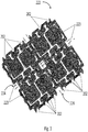
Figure 1 shows a known recess arrangement for side wettable leads of a semiconductor device; -
Figures 2a and2b illustrate a semiconductor device according to embodiments; -
Figure 3 illustrates a lead frame array for assembly of a semiconductor device according to embodiments; -
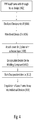
Figure 4 illustrates a flow chart for an example method of assembling a semiconductor device according to embodiments; and -
Figures 5a to 5e illustrate example steps for manufacturing a semiconductor device according to embodiments. - Referring now to
Figures 2a and2b asemiconductor device 200 in accordance with a preferred embodiment of the present invention is illustrated.Figure 2a is a transparent front isometric view, andFigure 2b is a bottom isometric view of thesemiconductor device 200. InFigure 2a thebody 212 of the device formed by an encapsulation material as discussed in more detail below, is shown in outline. Thedevice 200 is generally rectangular in shape and in one embodiment thedevice 200 is of the order of approximately 1.4mm X 1.2mm X 0.5mm (Length X Width X Height). - The
body 212 of thedevice 200 comprises a plurality ofleads 202 arranged on opposing side walls of thebody 212. In this embodiment the threeleads 202 are arranged on a first side wall and threeleads 202 are arranged on an opposing second side wall. In this way the skilled person will see that thedevice 200 is arranged as a DFN package. Thelead ends 202 may be arranged such that they are flush with bottom and side surfaces of thedevice body 212. Each of thelead ends 202 include arecess 204, which facilitates wicking of solder when thedevice 200 is attached to a substrate or PCB (not illustrated). The arrangement of therecesses 204 is discussed in more detail below. - As can be seen in
Figure 2a , thedevice 200 also comprises one of more semiconductor dies 216 mounted onrespective die pads 218 on and attached to the lead ends 202. Thedie pads 218 may be electrically connected to a respectivelead end 202, by extension of thelead end 202 to the die pad. Furthermore, the semiconductor dies may be electrically connected to the other lead ends 202 bybond wires 220. Alternatively, the semiconductor dies 216 may be flip-chip dies, having bumps on thedie pads 218 such that the semiconductor dies 216 can be electrically connected to the lead ends 202 by placing the die bonding pads in contact with the lead ends 202. The semiconductor dies 216, diepads 218 andbond wires 220 are encapsulated by the encapsulation material which may be a mould compound. - The lead ends 202 comprise a cut away portion or
recess 204 which has a height corresponding to the thickness of thelead end 202. In cross-section therecess 204 may be any appropriate shape such as semi-circular, semi-oval, or rectangular. Thelead end 202 also comprises abottom surface 210, which is generally exposed through a bottom surface of thesemiconductor device 200body 212. A top surface of the lead ends 202 opposite thebottom surface 210 is covered by aplate 206 which is affixed to the top surface of the lead ends 202 by anadhesive material 208. Theplate 206 may be formed of copper, Kapton tape or other suitable material. Likewise theplate 206 may be formed of a semiconductor material. By providing theplate 206, therecess 204 is covered at the top surface of the lead ends 202 whilst remining open at thebottom surface 210. This allows a solder fillet (not illustrated) connecting thesemiconductor device 200 to for example a PCB, to form up the entire surface of therecess 204, and also extend on to thebottom surface 210 of thelead end 202. - The thickness of the
plate 206 is such that it does not contribute to the overall final (moulded)device 200 height. In this regard the thickness of theplate 206 may be thinner than the semiconductor dies 216. Alternatively, the thickness of theplate 206 may be thinner than the semiconductor dies 216 and any connections thereto such asbond wires 220 or clip connections. The thickness of the plate may be in the region of 25 µm to 50µm and the thickness of the lead frame array 222 (discussed in more detail below) will be in the region of 100µm. Compared to the known standard leadframe thickness this results in a height reduction of up to approximately 60%. - This arrangement of
recess 204 top surface covered by theplate 206 ensures that mould compound does not contact therecess 204 during formation of thebody 212. This further results in alead end 202, and as discussed below, a lead frame, where the maximum thickness required is equal to the height of therecess 204. This results in a thinner leadframe and/or lead end for a given recess height because no lead end overhang portion is required, thus ensuring that the recess corresponds to the full height of the leadframe/lead end wettable portion and providing a full height solder fillet on the lead end when the device is mounted to, for example a PCB. -
Figure 3 illustrates a portion of alead frame array 222 used to assemble thesemiconductor device 200, with four individual lead frames 223 being illustrated. The lead frames 223 are separable from each other, as discussed below, by sawstreets 224, which run in the X-direction, and sawstreets 226, which run in the Y-direction. Each of the lead frames 223 comprises six lead ends 202, three on one side and three on an opposing side which extend from the opposing sides of the lead frames 223. Thelead frame array 222 may be formed from a sheet of conductive metal, such as copper, and may be pre-plated (PPF) as shown inFigure 4 or, not illustrated, post-plated with Sn on either the PPF or Cu surface. Thelead frame array 222 may be etched or stamped at the lead ends 202 to form therespective recesses 204. - Through holes 202 (which form the recesses after singulation) extend through the
lead frame array 222 and are provided in the vicinity of thesaw lanes 224. The through width of the throughholes 202 are bigger than thesaw lanes 224 such that following singulation, as discussed below, the recesses remain that extend to the full height of the lead ends/lead frame array. The depth of therecesses 204 are the full height of the lead frame thickness and can be achieved by a standard lead frame full etch or cutting process. Thedie pads 218 are sized and shaped to receive semiconductor dies 216. - Lead frame arrays formed from a sheet of metal, such as copper, etching of lead frame arrays, and plating of lead frame arrays are outside the scope of the present disclosure and thus not necessary for a complete understanding of the present invention.
-
Figure 4 is a flow chart illustrating an example method of manufacturing asemiconductor device 200 according to an embodiment. - The method begins at
step 402 by providing alead frame array 222 of the type described above and illustrated inFigure 5a . A plating step may be performed to plate the leads with a layer of Nickel, Palladium or Gold to prevent corrosion. The plating step can plate the entire lead frame or only selected portions thereof, as desired. The plating layer imparts solderability or solder wettability during a soldering process as well as protecting the exposed surfaces of the lead frame from corrosion. - At step 404 a
semiconductor die 216 is mounted on and attached to thedie pad 218 of the lead frame as illustrated inFigure 5b . The semiconductor die 216 may be attached by any appropriate adhesive layer, such as solder, eutectic material, double-sided adhesive tape and so on which may allow for electrical connection of the semiconductor die to the die pad. Alternatively, the semiconductor die 216 may be attached to thedie pad 218 such that there is no electrical connection between the die pad and the semiconductor die. Following placement of the semiconductor die 216, wire bonding pads arranged on the semiconductor die 216 may be electrically connected to respective wire bonding pads of the lead ends 202 withbond wires 220, atstep 406, and as illustrated inFigure 5b . - In an alternative method, the die may be a flip-chip die and have solder bumps on the die bond pads and then the die is mounted on the lead frame with the die active side facing the lead frame such that the die bond pads are in direct contact with the lead ends.
- Following placement of the semiconductor dies 216, the process continues at
step 408 as illustrated inFigure 5c , wherebycover plates 206 may be attached on the lead frame array, by means of a suitable adhesive, over the each of the throughholes 202 along the direction of the saw lanes. WhilstFigure 5c , illustrates a discrete cover plate for covering one respective through hole,Figure 5d illustrates that thecover plate 206 may arranged as single cover plate for covering a plurality of through holes. As an alternative, the cover plate orplates 206 may be pre-applied to the leadframe frame array. - The placement of the
cover plate step 408 is followed by an encapsulation ormoulding step 410 in which the lead frame, die, cover plate and bond wires are covered withmould compound 212, as is shown inFigure 5e . Themoulding step 410 preferably comprises a mould array process (MAP) where several assemblies formed on a lead frame array are all moulded at the same time, as shown inFigure 5e . - After the
moulding step 410, laser marking is performed instep 412 and if there is a tape on a bottom surface of the lead frame array, then the tape is removed in a detaping step. - The assemblies are then separated from each other in a
singulation step 414 in which a saw blade is run along the saw streets, thereby cutting and separating the simultaneously assembled devices from each other, as illustrated inFigure 5e . The singulated QFN semiconductor devices of the type described above with respect toFigure 2b may then be inspected, tested and packed for shipment. - The above describes DFN arrangement, however the skilled person will all appreciate that the present disclosure is also applicable to a QFN arrangement and any number of leads may be arranged on respective sides of the semiconductor device.
- Particular and preferred aspects of the invention are set out in the accompanying independent claims. Combinations of features from the dependent and/or independent claims may be combined as appropriate and not merely as set out in the claims.
- The scope of the present disclosure includes any novel feature or combination of features disclosed therein either explicitly or implicitly or any generalisation thereof irrespective of whether or not it relates to the claimed invention or mitigate against any or all of the problems addressed by the present invention. The applicant hereby gives notice that new claims may be formulated to such features during prosecution of this application or of any such further application derived therefrom. In particular, with reference to the appended claims, features from dependent claims may be combined with those of the independent claims and features from respective independent claims may be combined in any appropriate manner and not merely in specific combinations enumerated in the claims.
- Features which are described in the context of separate embodiments may also be provided in combination in a single embodiment. Conversely, various features which are, for brevity, described in the context of a single embodiment, may also be provided separately or in any suitable sub combination.
- Term "comprising" does not exclude other elements or steps, the term "a" or "an" does not exclude a plurality. Reference signs in the claims shall not be construed as limiting the scope of the claims.
Claims (15)
- A flank wettable semiconductor device, comprising:a lead frame including a plurality of leads comprising a lead end portion;a semiconductor die mounted on the lead frame;wherein the lead end portion comprises a recess portion having a height that corresponds to a thickness of the lead end portion, and a plate member mounted on the leadframe at the lead end portion.
- The flank wettable semiconductor device of claim 1, further comprising an encapsulation material that encapsulates the semiconductor die, the lead frame and partially encapsulates the plate member and the lead end portion.
- The flank wettable semiconductor device of claims 1 or 2, wherein the plate member is arranged over a top portion of the recess portion.
- The flank wettable semiconductor device of claims 1 to 3, wherein the recess portion is wettable with a solder material.
- The flank wettable semiconductor device of claims 1 to 4, further comprising a coating of protective metal or metal alloy formed on the recess portion.
- The flank wettable semiconductor device of claim 5, wherein the coating comprises tin or a tin alloy.
- The flank wettable semiconductor device of claims 5 to 6 wherein the coating is applied to the recess portion of the leads by electro-plating or electro-deposition prior to the device being separated from an adjacent device during assembly.
- The flank wettable semiconductor device of any preceding claim, further comprising a plurality of bond wires that electrically connect the semiconductor die with the leads.
- A method of manufacturing a flank wettable semiconductor device, the method comprising:providing an array of lead frames, wherein individual lead frames are separated by saw streets and each lead frame has a plurality of leads comprising a lead end portion;mounting and attaching semiconductor dies to respective ones of the lead frames;mounting and attaching a plate member on the leadframe at the lead end portion;encapsulating the dies with an encapsulation material;cutting the lead frame array along the saw streets to separate individual devices from adjacent devices, wherein the lead end portion comprises a recess portion having a height that corresponds to a thickness of the lead end portion.
- The method of claim 9, wherein the plate member is mounted on over a top portion of the recess portion.
- The method of claim 9 or 10, wherein the recess portion is wettable with a solder material.
- The method of claims 9 to 11, further comprising providing a coating of protective metal or metal alloy on the recess portion.
- The method of claim 12, wherein the coating comprises tin or a tin alloy.
- The method of claim 12 or 13 wherein the coating is applied to the recess portion of the leads by electro-plating or electro-deposition prior to the device being separated from an adjacent device during assembly.
- The method of claims 9 to 14, further comprising a plurality of bond wires that electrically connect the semiconductor die with the leads.
Priority Applications (2)
| Application Number | Priority Date | Filing Date | Title |
|---|---|---|---|
| EP19172982.1A EP3736857A1 (en) | 2019-05-07 | 2019-05-07 | Through hole side wettable flank |
| US16/865,533 US11227820B2 (en) | 2019-05-07 | 2020-05-04 | Through hole side wettable flank |
Applications Claiming Priority (1)
| Application Number | Priority Date | Filing Date | Title |
|---|---|---|---|
| EP19172982.1A EP3736857A1 (en) | 2019-05-07 | 2019-05-07 | Through hole side wettable flank |
Publications (1)
| Publication Number | Publication Date |
|---|---|
| EP3736857A1 true EP3736857A1 (en) | 2020-11-11 |
Family
ID=66448371
Family Applications (1)
| Application Number | Title | Priority Date | Filing Date |
|---|---|---|---|
| EP19172982.1A Withdrawn EP3736857A1 (en) | 2019-05-07 | 2019-05-07 | Through hole side wettable flank |
Country Status (2)
| Country | Link |
|---|---|
| US (1) | US11227820B2 (en) |
| EP (1) | EP3736857A1 (en) |
Cited By (1)
| Publication number | Priority date | Publication date | Assignee | Title |
|---|---|---|---|---|
| US20240006276A1 (en) * | 2022-06-29 | 2024-01-04 | Nexperia B.V. | Method of manufacturing semiconductor package assembly and a semiconductor package assembly manufactured using this method |
Families Citing this family (3)
| Publication number | Priority date | Publication date | Assignee | Title |
|---|---|---|---|---|
| US20220302013A1 (en) * | 2021-03-19 | 2022-09-22 | Advanced Semiconductor Engineering Korea, Inc. | Semiconductor device packages and methods of manufacturing the same |
| US12538812B2 (en) | 2023-02-07 | 2026-01-27 | Semiconductor Components Industries, Llc | Semiconductor packages with wettable flanks and related methods |
| FR3158588A1 (en) * | 2024-01-19 | 2025-07-25 | Stmicroelectronics International N.V. | Electronic component manufacturing process |
Citations (2)
| Publication number | Priority date | Publication date | Assignee | Title |
|---|---|---|---|---|
| US20110108965A1 (en) * | 2009-11-12 | 2011-05-12 | Hess Kevin J | Semiconductor device package |
| US20130277817A1 (en) * | 2012-04-20 | 2013-10-24 | Shinko Electric Industries Co., Ltd. | Lead frame, semiconductor package, and manufacturing method of the same |
Family Cites Families (7)
| Publication number | Priority date | Publication date | Assignee | Title |
|---|---|---|---|---|
| TW498443B (en) * | 2001-06-21 | 2002-08-11 | Advanced Semiconductor Eng | Singulation method for manufacturing multiple lead-free semiconductor packages |
| US6608366B1 (en) * | 2002-04-15 | 2003-08-19 | Harry J. Fogelson | Lead frame with plated end leads |
| US8329509B2 (en) * | 2010-04-01 | 2012-12-11 | Freescale Semiconductor, Inc. | Packaging process to create wettable lead flank during board assembly |
| CN102237280A (en) * | 2010-04-23 | 2011-11-09 | 飞思卡尔半导体公司 | Semiconductor device assembling method comprising step of saw singulation |
| US8841758B2 (en) * | 2012-06-29 | 2014-09-23 | Freescale Semiconductor, Inc. | Semiconductor device package and method of manufacture |
| US9578744B2 (en) * | 2014-12-22 | 2017-02-21 | Stmicroelectronics, Inc. | Leadframe package with pre-applied filler material |
| US20180122731A1 (en) * | 2016-11-02 | 2018-05-03 | Texas Instruments Incorporated | Plated ditch pre-mold lead frame, semiconductor package, and method of making same |
-
2019
- 2019-05-07 EP EP19172982.1A patent/EP3736857A1/en not_active Withdrawn
-
2020
- 2020-05-04 US US16/865,533 patent/US11227820B2/en active Active
Patent Citations (2)
| Publication number | Priority date | Publication date | Assignee | Title |
|---|---|---|---|---|
| US20110108965A1 (en) * | 2009-11-12 | 2011-05-12 | Hess Kevin J | Semiconductor device package |
| US20130277817A1 (en) * | 2012-04-20 | 2013-10-24 | Shinko Electric Industries Co., Ltd. | Lead frame, semiconductor package, and manufacturing method of the same |
Cited By (1)
| Publication number | Priority date | Publication date | Assignee | Title |
|---|---|---|---|---|
| US20240006276A1 (en) * | 2022-06-29 | 2024-01-04 | Nexperia B.V. | Method of manufacturing semiconductor package assembly and a semiconductor package assembly manufactured using this method |
Also Published As
| Publication number | Publication date |
|---|---|
| US11227820B2 (en) | 2022-01-18 |
| US20200357728A1 (en) | 2020-11-12 |
Similar Documents
| Publication | Publication Date | Title |
|---|---|---|
| US8685795B2 (en) | Flank wettable semiconductor device | |
| US6940154B2 (en) | Integrated circuit package and method of manufacturing the integrated circuit package | |
| US7816769B2 (en) | Stackable packages for three-dimensional packaging of semiconductor dice | |
| US7405106B2 (en) | Quad flat no-lead chip carrier with stand-off | |
| US11227820B2 (en) | Through hole side wettable flank | |
| US20030006055A1 (en) | Semiconductor package for fixed surface mounting | |
| US9153529B2 (en) | Pre-soldered leadless package | |
| KR101807878B1 (en) | Semiconductor device | |
| EP3840039B1 (en) | A semiconductor device and corresponding method | |
| EP3319122B1 (en) | Semiconductor device with wettable corner leads | |
| US20100200972A1 (en) | BGA package with leads on chip | |
| KR20020052930A (en) | A semiconductor device and method of manufacturing the same | |
| US11004742B2 (en) | Methods and apparatus for an improved integrated circuit package | |
| US8697496B1 (en) | Method of manufacture integrated circuit package | |
| US20110108967A1 (en) | Semiconductor chip grid array package and method for fabricating same | |
| EP3693992B1 (en) | Surface mount semiconductor device and method of manufacture | |
| US20200321228A1 (en) | Method of manufacturing a lead frame, method of manufacturing an electronic apparatus, and electronic apparatus | |
| EP4657521A1 (en) | A method of fabricating a semiconductor integrated circuits package | |
| JP2003197828A (en) | Resin-sealing semiconductor device | |
| JP4311294B2 (en) | Electronic device and manufacturing method thereof | |
| JP2000150761A (en) | Resin-sealed semiconductor device and method of manufacturing the same |
Legal Events
| Date | Code | Title | Description |
|---|---|---|---|
| PUAI | Public reference made under article 153(3) epc to a published international application that has entered the european phase |
Free format text: ORIGINAL CODE: 0009012 |
|
| STAA | Information on the status of an ep patent application or granted ep patent |
Free format text: STATUS: THE APPLICATION HAS BEEN PUBLISHED |
|
| AK | Designated contracting states |
Kind code of ref document: A1 Designated state(s): AL AT BE BG CH CY CZ DE DK EE ES FI FR GB GR HR HU IE IS IT LI LT LU LV MC MK MT NL NO PL PT RO RS SE SI SK SM TR |
|
| AX | Request for extension of the european patent |
Extension state: BA ME |
|
| STAA | Information on the status of an ep patent application or granted ep patent |
Free format text: STATUS: THE APPLICATION IS DEEMED TO BE WITHDRAWN |
|
| 18D | Application deemed to be withdrawn |
Effective date: 20210512 |