EP3734848A1 - Analog signal input/output device and control method for analog signal input/output device - Google Patents
Analog signal input/output device and control method for analog signal input/output device Download PDFInfo
- Publication number
- EP3734848A1 EP3734848A1 EP18894633.9A EP18894633A EP3734848A1 EP 3734848 A1 EP3734848 A1 EP 3734848A1 EP 18894633 A EP18894633 A EP 18894633A EP 3734848 A1 EP3734848 A1 EP 3734848A1
- Authority
- EP
- European Patent Office
- Prior art keywords
- analog signal
- input
- output
- signal input
- level
- Prior art date
- Legal status (The legal status is an assumption and is not a legal conclusion. Google has not performed a legal analysis and makes no representation as to the accuracy of the status listed.)
- Granted
Links
Images


Classifications
-
- H—ELECTRICITY
- H05—ELECTRIC TECHNIQUES NOT OTHERWISE PROVIDED FOR
- H05B—ELECTRIC HEATING; ELECTRIC LIGHT SOURCES NOT OTHERWISE PROVIDED FOR; CIRCUIT ARRANGEMENTS FOR ELECTRIC LIGHT SOURCES, IN GENERAL
- H05B45/00—Circuit arrangements for operating light-emitting diodes [LED]
- H05B45/10—Controlling the intensity of the light
-
- G—PHYSICS
- G01—MEASURING; TESTING
- G01D—MEASURING NOT SPECIALLY ADAPTED FOR A SPECIFIC VARIABLE; ARRANGEMENTS FOR MEASURING TWO OR MORE VARIABLES NOT COVERED IN A SINGLE OTHER SUBCLASS; TARIFF METERING APPARATUS; MEASURING OR TESTING NOT OTHERWISE PROVIDED FOR
- G01D7/00—Indicating measured values
-
- G—PHYSICS
- G01—MEASURING; TESTING
- G01J—MEASUREMENT OF INTENSITY, VELOCITY, SPECTRAL CONTENT, POLARISATION, PHASE OR PULSE CHARACTERISTICS OF INFRARED, VISIBLE OR ULTRAVIOLET LIGHT; COLORIMETRY; RADIATION PYROMETRY
- G01J1/00—Photometry, e.g. photographic exposure meter
- G01J1/42—Photometry, e.g. photographic exposure meter using electric radiation detectors
- G01J1/44—Electric circuits
-
- G—PHYSICS
- G01—MEASURING; TESTING
- G01V—GEOPHYSICS; GRAVITATIONAL MEASUREMENTS; DETECTING MASSES OR OBJECTS; TAGS
- G01V8/00—Prospecting or detecting by optical means
- G01V8/10—Detecting, e.g. by using light barriers
-
- G—PHYSICS
- G09—EDUCATION; CRYPTOGRAPHY; DISPLAY; ADVERTISING; SEALS
- G09F—DISPLAYING; ADVERTISING; SIGNS; LABELS OR NAME-PLATES; SEALS
- G09F13/00—Illuminated signs; Luminous advertising
- G09F13/20—Illuminated signs; Luminous advertising with luminescent surfaces or parts
-
- H—ELECTRICITY
- H04—ELECTRIC COMMUNICATION TECHNIQUE
- H04B—TRANSMISSION
- H04B3/00—Line transmission systems
- H04B3/02—Details
- H04B3/46—Monitoring; Testing
-
- H—ELECTRICITY
- H05—ELECTRIC TECHNIQUES NOT OTHERWISE PROVIDED FOR
- H05B—ELECTRIC HEATING; ELECTRIC LIGHT SOURCES NOT OTHERWISE PROVIDED FOR; CIRCUIT ARRANGEMENTS FOR ELECTRIC LIGHT SOURCES, IN GENERAL
- H05B47/00—Circuit arrangements for operating light sources in general, i.e. where the type of light source is not relevant
- H05B47/10—Controlling the light source
Definitions
- the present invention relates to an analog signal input/output device which performs at least one of input and output of an analog signal.
- Patent Literature 1 discloses, as a device that inputs or outputs an analog signal, a process input/output device which is equipped to perform a calibration procedure and display the calibration procedure. Specifically, the process input/output device controls lighting of an LED, depending on a step of a calibration test of an input/output circuit.
- Patent Literature 1 Japanese Patent Application Publication Tokukai No. 2014-178785 (Published on September 25, 2014 )
- the need may arise to check whether they have been properly connected. Further, in a case where a failure occurs during the operation of the analog signal input/output device, the need may arise to determine the cause of the failure. For example, the need may arise to determine whether the failure is caused by the analog signal input/output device or whether the failure is caused by a factor outside the analog signal input/output device (defective wiring or a failure of an apparatus to which the analog signal input/output device is connected). In such a case, it is important to check the input or output level of the analog signal in the analog signal input/output device.
- the conventional technique as described above is not a technique based on the viewpoint of indicating to the user the input or output level of the analog signal.
- a configuration for displaying the input or output level of an analog signal such as a seven-segment LED, a liquid crystal display device, or an analog meter. Installing such a configuration in the analog signal input/output device increases a production cost. Further, in order to install the configuration as described above in the analog signal input/output device, it is necessary to provide a space for installing the configuration.
- an analog signal input/output device in accordance with an aspect of the present invention is an analog signal input/output device which includes a light emitting element and performs at least one of input and output of an analog signal, the analog signal input/output device including: an input/output level detecting section configured to detect at least one of an input level and an output level of the analog signal; and a light emission control section configured to control an on and off pattern of light emission of the light emitting element in accordance with the input level or the output level of the analog signal.
- a method of controlling an analog signal input/output device in accordance with an aspect of the present invention is a method of controlling an analog signal input/output device which includes a light emitting element and performs at least one of input and output of an analog signal, the method including: an input/output level detecting step of detecting at least one of an input level and an output level of the analog signal; and a light emission controlling step of controlling an on and off pattern of light emission of the light emitting element in accordance with the input level or the output level of the analog signal.
- Fig. 2 is a diagram illustrating one example of an application for an analog signal input/output device in accordance with the present embodiment. First, an overview of an application of the analog signal input/output device will be discussed with reference to Fig. 2 .
- an analog signal input device 1 is a device to which an analog signal is inputted via an input/output terminal 11 from an analog signal output apparatus such as a sensor.
- the analog signal input device 1 may be an A/D converter for converting an analog signal into a digital signal.
- the analog signal input device 1 outputs a digital signal to a controller 3 via a controller communication terminal 17.
- the analog signal input device 1 detects an input level of an inputted analog signal.
- the analog signal input device 1 controls an on and off pattern of light emission of an LED (light emitting element) 15, which is provided in the analog signal input device 1, in accordance with the detected input level of the analog signal. As such, the analog signal input device 1 allows the LED 15 to light up in a pattern which varies depending on the input level of the analog signal.
- the analog signal input device 1 which indicates an input level of an inputted analog signal is provided.
- the present embodiment may be applied to an analog signal output device, instead of the analog signal input device 1.
- the analog signal output device converts, for example, a digital signal outputted from the controller 3 into an analog signal.
- the analog signal output device outputs the analog signal to an apparatus which is driven by an analog signal (e.g., a heater that requires temperature control).
- an analog signal e.g., a heater that requires temperature control
- the present embodiment may be applied to a device for inputting an analog signal and a digital signal, a device for outputting an analog signal and a digital signal, a device for inputting and outputting an analog signal and a digital signal, and the like. These devices indicate at least one of an input level and an output level of an analog signal.
- the above-described configuration it is possible to indicate the input or output level of an analog signal by a light emission pattern of a single LED.
- the above-described configuration achieves reduction in production cost of the analog signal input/output device, in comparison to the configuration in which the input or output level of an analog signal is numerically displayed by a seven-segment LED, the configuration in which the input or output level of an analog signal is indicated by liquid crystal display, the configuration in which the input or output level of an analog signal is indicated by an analog meter or the like, and other configuration.
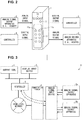
- Fig. 3 is a diagram illustrating an overview of one example of a system 9 in accordance with the present embodiment.
- the system 9 includes an analog signal input device, an analog signal output apparatus 2, a controller 3, a support tool 4, a display input device 5, and a communication coupler 6.
- the analog signal input device 1 is a relay device which relays data between a high-level network, which includes the controller 3 and others, and the analog signal output apparatus 2.
- the analog signal input device 1 is an A/D converter.
- the communication coupler 6 is a relay device which relays communication between the high-level network and the analog signal input device 1.
- the communication coupler 6 relays communication between an apparatus included in the high-level network and the analog signal input device 1.
- the analog signal output apparatus 2 is an apparatus which is connected to the analog signal input device 1 and is subject to control by the controller 3.
- Examples of the analog signal output apparatus 2 include various kinds of sensors such as a photoelectronic sensor and a proximity sensor.
- the controller 3 is a control device which performs centralized control of the whole of the system 9, and is also referred to as programmable logic controller (PLC).
- PLC programmable logic controller
- the controller 3 operates as a master device of the analog signal input device 1 in the system 9.
- the support tool 4 is a device which is used, in a state of being connected to the system 9, for various settings of the system 9 such as operation settings of the analog signal input device 1.
- the support tool 4 can be connected to the system 9 via the controller 3.
- the support tool 4 can be an information processing device such as a personal computer and can also be a portable information processing device such as a notebook computer. Note that the support tool 4 may be adapted to be connected to the analog signal input device 1 via the communication coupler 6 to perform various settings.
- the display input device 5 is, for example, a display input device of a touch panel type.
- a user of the system 9 can operate the controller 3 via the display input device 5 and can check the operation status of the system 9 on the display input device 5.
- the controller 3 may include the configuration, which is provided in the analog signal input device 1, for indicating the input level (or the output level) of an analog signal.
- Fig. 1 is a block diagram illustrating one example of main components of the analog signal input device 1 in accordance with the present embodiment. As described above, in the present embodiment, an example case where the analog signal input device 1 is an A/D converter for converting an inputted analog signal into a digital signal is provided.
- the analog signal input device 1 is an A/D converter for converting an inputted analog signal into a digital signal.
- the analog signal input device 1 includes an input terminal 11a, an output terminal 11b, a controller communication terminal 17, a control section 13, a storage section 14, the LED 15, and an A/D converting section 16.
- the input terminal 11a accepts input of a signal from an external apparatus.
- the input terminal 11a particularly accepts input of an analog signal from the analog signal output apparatus 2.
- the output terminal 11b outputs output data to an external apparatus.
- the controller communication terminal 17 outputs a digital signal to the controller 3 through the communication coupler 6.
- the input terminal 11a, the output terminal 11b, and the controller communication terminal 17 may be two or more input terminals 11a, two or more output terminals 11b, and two or more controller communication terminals 17, respectively, or may be a single input terminal 11a, a single output terminal 11b, and a single controller communication terminal 17, respectively.
- An analog signal (A)/digital signal (D) converting section 16 receives an analog signal from the analog signal output apparatus 2 through the input terminal 11a.
- the A/D converting section 16 converts the received analog signal into a digital signal.
- the A/D converting section 16 transmits the digital signal to the control section 13.
- the A/D converting section 16 transmits the digital signal to a voltage detecting section 130, in particular.
- control section 13 may perform a filtering process or the like for removing noise of the digital signal.
- control section 13 transmits the digital signal subjected to the filtering process to the controller 3 through the controller communication terminal 17 and the communication coupler 6.
- the control section 13 includes a central processing unit (CPU), a random access memory (RAM), a read only memory (ROM) and others, and controls each of the constituent components in accordance with information processing.
- the control section 13 includes the voltage detecting section 130, a relative value converting section 131, and an LED lighting control section (light emission control section) 132.
- the voltage detecting section 130 detects an input level of an analog signal having been inputted through the input terminal 11a. Specifically, the voltage detecting section 130 detects a voltage level of the analog signal based on a digital signal having been received from the A/D converting section 16. The voltage detecting section 130 transmits the detected voltage level to the relative value converting section 131.
- the relative value converting section 131 converts an analog signal input or output level having been received from the voltage detecting section 130 into a relative value relative to one analog signal input/output level range which has been set through selection from among different analog signal input/output level ranges. This will be specifically discussed below.
- Fig. 4 is a diagram showing correspondence between a voltage level of an analog input (input/output) signal and a relative value for the voltage level relative to a range.
- the analog signal input (input/output) level range is set through selection from among the following ranges: range A (range of 0V to +10V); range B (range of 0V to +5V); and range C (range of -10V to +10V).
- the analog signal input device 1 may be configured to set any of the input level ranges in response to a selection operation which has been performed by a user on the support tool 4 and then has been accepted by the analog signal input device 1.
- the analog signal input device 1 may be configured to accept input operations for a maximum value and a minimum value of the range on the support tool 4 and then set any input level range.
- the set range may be stored as range information 141 in the storage section 14.
- the relative value converting section 131 refers to the range information 141 and then determines a relative value, for a voltage level of an analog signal, relative to the set range. For example, as shown in Fig. 4 , in a case where the range A (range of 0V to +10V) is set, the relative value converting section 131 determines a relative value in a manner as described below.
- the relative value converting section 131 determines, on a percentage basis, a relative value for an inputted analog signal, on the assumption that 0 V, which is a minimum value of the range, is regarded as 0%, and +10 V, which is a maximum value of the range, is regarded as 100%.
- the relative value converting section 131 determines a relative value in a manner as described below.
- the relative value converting section 131 determines, on a percentage basis, a relative value for an inputted analog signal, on the assumption that 0 V, which is a minimum value of the range, is regarded as 0%, and +5 V, which is a maximum value of the range, is regarded as 100%.
- the relative value converting section 131 determines a relative value in a manner as described below.
- the relative value converting section 131 determines, on a percentage basis, a relative value for an inputted analog signal, on the assumption that -10 V, which is a minimum value of the range, is regarded as 0%, and +10 V, which is a maximum value of the range, is regarded as 100%.
- the relative value converting section 131 transmits, to the LED lighting control section 132, the determined relative value for the analog signal.
- the LED lighting control section 132 controls an on and off pattern of light emission of the light emitting element in accordance with an input level of an analog signal.
- the LED lighting control section 132 controls an on and off pattern of light emission of the LED 15 in accordance with a relative value having been received from the relative value converting section 131.
- the LED lighting control section 132 may be configured to refer to lighting pattern information, stored in the storage section 14, indicative of lighting patterns of the LED 15 and then control light emission of the LED 15 in accordance with the lighting pattern information.
- the lighting pattern information 142 is information indicative of correspondences between the lighting patterns of the LED 15 and the relative values. The following description will discuss an example of a manner in which the LED lighting control section 132 performs on-off control of light emission of the LED 15.
- Example 1 of lighting control of LED 15 Control of turning-on time and turning-off time in a predetermined period of time
- the LED lighting control section 132 may be configured to determine a turning-on (on) time of the LED 15 and a turning-off (off) time thereof in a predetermined period of time in accordance with the relative value (percentage) so as to control the turning on or blinking of the LED 15. For example, the LED lighting control section 132 controls the turning on and turning off of the LED 15 in a period of one second in a manner as described below. In a case where the relative value is 0%, the LED lighting control section 132 determines that the turning-off time is one second, and does not turn on the LED 15.
- the LED lighting control section 132 determines that the turning-on time is 0.1 second and the turning-off time is 0.9 second, and causes the LED 15 to blink in accordance with the turning-on time and the turning-off time. In a case where the relative value is 90%, the LED lighting control section 132 determines that the turning-on time is 0.9 second and the turning-off time is 0.1 second, and causes the LED 15 to blink in accordance with the turning-on time and the turning-off time. In a case where the relative value is 100%, the LED lighting control section 132 determines that the turning-on time is one second, and turns on the LED 15 throughout the period of one second. That is, the LED lighting control section 132 performs control such that the length of the turning-on time of the LED 15 in a predetermined period of time increases with increase in the relative value.
- the LED lighting control section 132 may be configured to determine a blinking period of the LED 15 in accordance with the relative value so as to control the turning on or blinking of the LED 15.
- the LED lighting control section 132 does not turn on the LED 15.
- the LED lighting control section 132 causes the LED 15 to blink by turning on the LED 15 for one second and turning off the LED 15 for one second.
- the LED lighting control section 132 causes the LED 15 to blink by turning on the LED 15 for 0.8 second and turning off the LED 15 for 0.8 second.
- the LED lighting control section 132 causes the LED 15 to blink by turning on the LED 15 for 0.6 second and turning off the LED 15 for 0.6 second.
- the LED lighting control section 132 causes the LED 15 to blink by turning on the LED 15 for 0.4 second and turning off the LED 15 for 0.4 second. In a case where the relative value is 100%, the LED lighting control section 132 causes the LED 15 to blink by turning on the LED 15 for 0.2 second and turning off the LED 15 for 0.2 second. That is, the LED lighting control section 132 performs control such that the length of the blinking period of the LED 15 decreases with increase in the relative value.
- the relative value converting section 131 may be configured such that, in a case where the level of an inputted analog signal falls outside a set range, the relative value converting section 131 does not determine a relative value. According to the above-described configuration, in a case where the inputted analog signal does not correspond to the set range, light emission of the LED 15 is not controlled. This allows a user to recognize that the inputted analog signal does not correspond to the set range.
- the analog signal input device 1 may be configured to input a plurality of analog input signals simultaneously.
- the analog signal input device 1 may include a plurality of input terminals 11a and a plurality of LEDs 15.
- the input terminals 11a and the LEDs 15 may be in a one-to-one correspondence.
- the LED lighting control section 132 may control the lighting of the LEDs 15 corresponding to the input terminals 11a to indicate the levels of the analog input signals inputted through the input terminals 11a.
- information indicative of which of the LEDs 15 each of the input terminals 11a corresponds to may be stored in the storage section 14.
- the LED lighting control section 132 may be configured to refer to such information and then control lighting of the LEDs 15 in accordance with the information.
- the storage section 14 is, for example, an auxiliary storage device such as a flash memory or a solid-state drive, and stores the above-described range information 141, the above-described lighting pattern information 142, and others.
- the LED 15 emits light under control of the LED lighting control section 132.
- the LED 15 may be controlled to emit light even when any signal other than an analog signal is inputted or outputted. That is, the LED 15 may be shared not only for the purpose of indicating an input or output level of an analog signal but also for another purpose. For example, one LED 15 may emit light not only to indicate the input or output level of an analog signal but also to indicate the input of other signal (e.g., an external trigger signal). A signal targeted for input indication given by the LED 15 may be changed to another signal when a selection operation performed on the support tool 4 by the user is accepted.
- the above-described configuration eliminates the need for installing a plurality of light emitting elements on a purpose by purpose basis. Therefore, it is possible to reduce the production cost, and it is also possible to contribute to space saving.
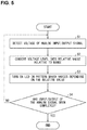
- Fig. 5 is a flowchart illustrating one example of the flow of processes carried out by the analog signal input device 1 in accordance with the present embodiment. The following description will discuss, with reference to Fig. 5 , one example of the flow of processes carried out by the analog signal input device 1.
- the voltage detecting section 130 detects a voltage level of an analog input signal (S1: input/output level detecting step).
- the relative value converting section 131 converts the voltage level of the analog input signal into a relative value (S2).
- the LED lighting control section 132 turns on the LED 15 in a pattern which varies depending on the relative value (S3: light emission controlling step).
- the process ends.
- the input of the analog signal has not been completed (NO in S4), the process returns to S1.
- Control blocks of the analog signal input device 1 can be realized by a logic circuit (hardware) provided in an integrated circuit (IC chip) or the like or can be alternatively realized by software.
- the analog signal input device 1 includes a computer that executes instructions of a program that is software realizing the foregoing functions.
- the computer for example, includes one or more processors and a computer-readable storage medium storing the program.
- An object of the present invention can be achieved by the processor of the computer reading and executing the program stored in the storage medium.
- the processor encompass a central processing unit (CPU).
- the storage medium encompass a "non-transitory tangible medium" such as a read only memory (ROM), a tape, a disk, a card, a semiconductor memory, and a programmable logic circuit.
- the computer may further include a random access memory (RAM) or the like in which the program is loaded.
- the program may be made available to the computer via any transmission medium (such as a communication network and a broadcast wave) which allows the program to be transmitted.
- a transmission medium such as a communication network and a broadcast wave
- an aspect of the present invention can also be achieved in the form of a computer data signal in which the program is embodied via electronic transmission and which is embedded in a carrier wave.
- the present invention is not limited to the embodiments, but can be altered by a skilled person in the art within the scope of the claims.
- the present invention also encompasses, in its technical scope, any embodiment derived by combining technical means disclosed in differing embodiments.
- the present invention can be expressed as follows.
- An analog signal input/output device in accordance with an aspect of the present invention is an analog signal input/output device which includes a light emitting element and performs at least one of input and output of an analog signal, the analog signal input/output device including: an input/output level detecting section configured to detect at least one of an input level and an output level of the analog signal; and a light emission control section configured to control an on and off pattern of light emission of the light emitting element in accordance with the input level or the output level of the analog signal.
- a method of controlling an analog signal input/output device in accordance with an aspect of the present invention is a method of controlling an analog signal input/output device which includes a light emitting element and performs at least one of input and output of an analog signal, the method including: an input/output level detecting step of detecting at least one of an input level and an output level of the analog signal; and a light emission controlling step of controlling an on and off pattern of light emission of the light emitting element in accordance with the input level or the output level of the analog signal.
- the above-described configuration it is possible to indicate the input level and/or the output level of the analog signal by a light emission pattern of one light emitting element.
- the above-described configuration achieves reduction in production cost, in comparison to, for example, the configuration in which the input level and/or the output level of an analog signal is numerically displayed by a seven-segment LED, the configuration in which the input level and/or the output level of an analog signal is indicated by liquid crystal display, the configuration in which the input level and/or the output level of an analog signal is indicated by an analog meter or the like, and other configuration.
- An analog signal input/output device in accordance with an aspect of the present invention includes a relative value converting section configured to convert a detected input or output level of the analog signal into a relative value relative to one analog signal input/output level range which has been set through selection from among different analog signal input/output level ranges, the light emission control section being configured to control the on and off pattern of the light emission of the light emitting element in accordance with the relative value.
- An analog signal input/output device in accordance with an aspect of the present invention is configured such that the one analog signal input/output level range is set in response to a selection operation which has been performed by a user and then has been accepted by the analog signal input/output device.
- An analog signal input/output device in accordance with an aspect of the present invention is configured such that the light emitting element is controlled to emit light even when any signal other than the analog signal is inputted or outputted.
- the above-described configuration eliminates the need for installing a plurality of light emitting elements on a purpose by purpose basis. Therefore, it is possible to reduce the production cost of the analog signal input/output device, and it is also possible to contribute to space saving.
Landscapes
- Physics & Mathematics (AREA)
- General Physics & Mathematics (AREA)
- Engineering & Computer Science (AREA)
- Life Sciences & Earth Sciences (AREA)
- General Life Sciences & Earth Sciences (AREA)
- Geophysics (AREA)
- Spectroscopy & Molecular Physics (AREA)
- Computer Networks & Wireless Communication (AREA)
- Signal Processing (AREA)
- Theoretical Computer Science (AREA)
- Circuit Arrangement For Electric Light Sources In General (AREA)
- Illuminated Signs And Luminous Advertising (AREA)
Abstract
Description
- The present invention relates to an analog signal input/output device which performs at least one of input and output of an analog signal.
- For example,
Patent Literature 1 discloses, as a device that inputs or outputs an analog signal, a process input/output device which is equipped to perform a calibration procedure and display the calibration procedure. Specifically, the process input/output device controls lighting of an LED, depending on a step of a calibration test of an input/output circuit. - Patent Literature 1: Japanese Patent Application Publication Tokukai No.
2014-178785 (Published on September 25, 2014 - In a case where connection between an analog signal input/output device and an external apparatus is made, the need may arise to check whether they have been properly connected. Further, in a case where a failure occurs during the operation of the analog signal input/output device, the need may arise to determine the cause of the failure. For example, the need may arise to determine whether the failure is caused by the analog signal input/output device or whether the failure is caused by a factor outside the analog signal input/output device (defective wiring or a failure of an apparatus to which the analog signal input/output device is connected). In such a case, it is important to check the input or output level of the analog signal in the analog signal input/output device.
- However, the conventional technique as described above is not a technique based on the viewpoint of indicating to the user the input or output level of the analog signal. For example, in order to display the input or output level of an analog signal, it is necessary to install, in the analog signal input/output device, a configuration for displaying the input or output level of an analog signal, such as a seven-segment LED, a liquid crystal display device, or an analog meter. Installing such a configuration in the analog signal input/output device increases a production cost. Further, in order to install the configuration as described above in the analog signal input/output device, it is necessary to provide a space for installing the configuration.
- It is an object of an aspect of the present invention to provide an analog signal input/output device capable of indicating an input or output level of an analog signal, at low production cost and without the need for a wide space to install a configuration for indicating the input or output level.
- In order to solve the above problems, an analog signal input/output device in accordance with an aspect of the present invention is an analog signal input/output device which includes a light emitting element and performs at least one of input and output of an analog signal, the analog signal input/output device including: an input/output level detecting section configured to detect at least one of an input level and an output level of the analog signal; and a light emission control section configured to control an on and off pattern of light emission of the light emitting element in accordance with the input level or the output level of the analog signal.
- Further, a method of controlling an analog signal input/output device in accordance with an aspect of the present invention is a method of controlling an analog signal input/output device which includes a light emitting element and performs at least one of input and output of an analog signal, the method including: an input/output level detecting step of detecting at least one of an input level and an output level of the analog signal; and a light emission controlling step of controlling an on and off pattern of light emission of the light emitting element in accordance with the input level or the output level of the analog signal.
- According to the aspects of the present invention, it is possible to indicate an input or output level of an analog signal by a light emission pattern of one light emitting element.
-
-
Fig. 1 is a block diagram illustrating one example of main components of an analog signal input device in accordance with an embodiment of the present invention. -
Fig. 2 is a diagram illustrating an overview of an application for an analog signal input/output device in accordance with an embodiment of the present invention. -
Fig. 3 is a diagram illustrating an overview of one example of a system in accordance with an embodiment of the present invention. -
Fig. 4 is a diagram showing correspondence between a voltage level of an analog input/output signal and a relative value for the voltage level relative to a range in accordance with an embodiment of the present invention. -
Fig. 5 is a flowchart illustrating one example of the flow of processes carried out by an analog signal input device in accordance with an embodiment of the present invention. - The following description will discuss an embodiment in accordance with an aspect of the present invention (hereinafter also referred to as "the present embodiment") with reference to the drawings.
-
Fig. 2 is a diagram illustrating one example of an application for an analog signal input/output device in accordance with the present embodiment. First, an overview of an application of the analog signal input/output device will be discussed with reference toFig. 2 . - As illustrated in
Fig. 2 , an analogsignal input device 1 is a device to which an analog signal is inputted via an input/output terminal 11 from an analog signal output apparatus such as a sensor. For example, the analogsignal input device 1 may be an A/D converter for converting an analog signal into a digital signal. In this case, the analogsignal input device 1 outputs a digital signal to acontroller 3 via acontroller communication terminal 17. The analogsignal input device 1 detects an input level of an inputted analog signal. The analogsignal input device 1 controls an on and off pattern of light emission of an LED (light emitting element) 15, which is provided in the analogsignal input device 1, in accordance with the detected input level of the analog signal. As such, the analogsignal input device 1 allows theLED 15 to light up in a pattern which varies depending on the input level of the analog signal. - Note that, in the present embodiment, a specific example for the analog
signal input device 1 which indicates an input level of an inputted analog signal is provided. Alternatively, as illustrated inFig. 2 , the present embodiment may be applied to an analog signal output device, instead of the analogsignal input device 1. In this case, the analog signal output device converts, for example, a digital signal outputted from thecontroller 3 into an analog signal. The analog signal output device outputs the analog signal to an apparatus which is driven by an analog signal (e.g., a heater that requires temperature control). By appropriately changing the configuration of the analogsignal input device 1, the analog signal output device indicates an output level of an analog signal by a light emission pattern of the LED. - Further, the present embodiment may be applied to a device for inputting an analog signal and a digital signal, a device for outputting an analog signal and a digital signal, a device for inputting and outputting an analog signal and a digital signal, and the like. These devices indicate at least one of an input level and an output level of an analog signal.
- With the above-described configuration, it is possible to indicate the input or output level of an analog signal by a light emission pattern of a single LED. As such, the above-described configuration achieves reduction in production cost of the analog signal input/output device, in comparison to the configuration in which the input or output level of an analog signal is numerically displayed by a seven-segment LED, the configuration in which the input or output level of an analog signal is indicated by liquid crystal display, the configuration in which the input or output level of an analog signal is indicated by an analog meter or the like, and other configuration. Further, with the above-described configuration, it is possible to save space necessary for providing a configuration for indicating the input or output level of an analog signal. Therefore, it is possible to improve the degree of freedom in the design of the analog signal input/output device.
-
Fig. 3 is a diagram illustrating an overview of one example of asystem 9 in accordance with the present embodiment. As illustrated inFig. 3 , thesystem 9 includes an analog signal input device, an analogsignal output apparatus 2, acontroller 3, asupport tool 4, adisplay input device 5, and acommunication coupler 6. - As illustrated in
Fig. 3 , the analogsignal input device 1 is a relay device which relays data between a high-level network, which includes thecontroller 3 and others, and the analogsignal output apparatus 2. In the present embodiment, an example case where the analogsignal input device 1 is an A/D converter is provided. - The
communication coupler 6 is a relay device which relays communication between the high-level network and the analogsignal input device 1. Thecommunication coupler 6 relays communication between an apparatus included in the high-level network and the analogsignal input device 1. - As illustrated in
Fig. 3 , the analogsignal output apparatus 2 is an apparatus which is connected to the analogsignal input device 1 and is subject to control by thecontroller 3. Examples of the analogsignal output apparatus 2 include various kinds of sensors such as a photoelectronic sensor and a proximity sensor. - The
controller 3 is a control device which performs centralized control of the whole of thesystem 9, and is also referred to as programmable logic controller (PLC). Thecontroller 3 operates as a master device of the analogsignal input device 1 in thesystem 9. - The
support tool 4 is a device which is used, in a state of being connected to thesystem 9, for various settings of thesystem 9 such as operation settings of the analogsignal input device 1. Thesupport tool 4 can be connected to thesystem 9 via thecontroller 3. Thesupport tool 4 can be an information processing device such as a personal computer and can also be a portable information processing device such as a notebook computer. Note that thesupport tool 4 may be adapted to be connected to the analogsignal input device 1 via thecommunication coupler 6 to perform various settings. - The
display input device 5 is, for example, a display input device of a touch panel type. A user of thesystem 9 can operate thecontroller 3 via thedisplay input device 5 and can check the operation status of thesystem 9 on thedisplay input device 5. - Further, in the
system 9 illustrated inFig. 3 , in a case where thecontroller 3 is configured to input/output an analog signal, thecontroller 3 may include the configuration, which is provided in the analogsignal input device 1, for indicating the input level (or the output level) of an analog signal. -
Fig. 1 is a block diagram illustrating one example of main components of the analogsignal input device 1 in accordance with the present embodiment. As described above, in the present embodiment, an example case where the analogsignal input device 1 is an A/D converter for converting an inputted analog signal into a digital signal is provided. - As illustrated in
Figs. 1 and2 , the analogsignal input device 1 includes aninput terminal 11a, anoutput terminal 11b, acontroller communication terminal 17, acontrol section 13, astorage section 14, theLED 15, and an A/D converting section 16. - The
input terminal 11a accepts input of a signal from an external apparatus. In the present embodiment, theinput terminal 11a particularly accepts input of an analog signal from the analogsignal output apparatus 2. Theoutput terminal 11b outputs output data to an external apparatus. Further, thecontroller communication terminal 17 outputs a digital signal to thecontroller 3 through thecommunication coupler 6. Theinput terminal 11a, theoutput terminal 11b, and thecontroller communication terminal 17 may be two ormore input terminals 11a, two ormore output terminals 11b, and two or morecontroller communication terminals 17, respectively, or may be asingle input terminal 11a, asingle output terminal 11b, and a singlecontroller communication terminal 17, respectively. - An analog signal (A)/digital signal (D) converting
section 16 receives an analog signal from the analogsignal output apparatus 2 through theinput terminal 11a. The A/D converting section 16 converts the received analog signal into a digital signal. The A/D converting section 16 transmits the digital signal to thecontrol section 13. In the present embodiment, the A/D converting section 16 transmits the digital signal to avoltage detecting section 130, in particular. - Further, the
control section 13 may perform a filtering process or the like for removing noise of the digital signal. For example, thecontrol section 13 transmits the digital signal subjected to the filtering process to thecontroller 3 through thecontroller communication terminal 17 and thecommunication coupler 6. - The
control section 13 includes a central processing unit (CPU), a random access memory (RAM), a read only memory (ROM) and others, and controls each of the constituent components in accordance with information processing. Thecontrol section 13 includes thevoltage detecting section 130, a relativevalue converting section 131, and an LED lighting control section (light emission control section) 132. - The
voltage detecting section 130 detects an input level of an analog signal having been inputted through theinput terminal 11a. Specifically, thevoltage detecting section 130 detects a voltage level of the analog signal based on a digital signal having been received from the A/D converting section 16. Thevoltage detecting section 130 transmits the detected voltage level to the relativevalue converting section 131. - The relative
value converting section 131 converts an analog signal input or output level having been received from thevoltage detecting section 130 into a relative value relative to one analog signal input/output level range which has been set through selection from among different analog signal input/output level ranges. This will be specifically discussed below. -
Fig. 4 is a diagram showing correspondence between a voltage level of an analog input (input/output) signal and a relative value for the voltage level relative to a range. As shown inFig. 4 , in the present embodiment, the analog signal input (input/output) level range is set through selection from among the following ranges: range A (range of 0V to +10V); range B (range of 0V to +5V); and range C (range of -10V to +10V). - The analog
signal input device 1 may be configured to set any of the input level ranges in response to a selection operation which has been performed by a user on thesupport tool 4 and then has been accepted by the analogsignal input device 1. Alternatively, the analogsignal input device 1 may be configured to accept input operations for a maximum value and a minimum value of the range on thesupport tool 4 and then set any input level range. For example, the set range may be stored asrange information 141 in thestorage section 14. - With the above-described configuration, it is possible to indicate an input or output level of an inputted or outputted analog signal in the range that the user desires.
- The relative
value converting section 131 refers to therange information 141 and then determines a relative value, for a voltage level of an analog signal, relative to the set range. For example, as shown inFig. 4 , in a case where the range A (range of 0V to +10V) is set, the relativevalue converting section 131 determines a relative value in a manner as described below. The relativevalue converting section 131 determines, on a percentage basis, a relative value for an inputted analog signal, on the assumption that 0 V, which is a minimum value of the range, is regarded as 0%, and +10 V, which is a maximum value of the range, is regarded as 100%. Further, in a case where the range B (range of 0V to +5V) is set, the relativevalue converting section 131 determines a relative value in a manner as described below. The relativevalue converting section 131 determines, on a percentage basis, a relative value for an inputted analog signal, on the assumption that 0 V, which is a minimum value of the range, is regarded as 0%, and +5 V, which is a maximum value of the range, is regarded as 100%. Further, in a case where the range C (range of -10V to +10V) is set, the relativevalue converting section 131 determines a relative value in a manner as described below. The relativevalue converting section 131 determines, on a percentage basis, a relative value for an inputted analog signal, on the assumption that -10 V, which is a minimum value of the range, is regarded as 0%, and +10 V, which is a maximum value of the range, is regarded as 100%. The relativevalue converting section 131 transmits, to the LEDlighting control section 132, the determined relative value for the analog signal. - The LED
lighting control section 132 controls an on and off pattern of light emission of the light emitting element in accordance with an input level of an analog signal. - Specifically, the LED
lighting control section 132 controls an on and off pattern of light emission of theLED 15 in accordance with a relative value having been received from the relativevalue converting section 131. For example, the LEDlighting control section 132 may be configured to refer to lighting pattern information, stored in thestorage section 14, indicative of lighting patterns of theLED 15 and then control light emission of theLED 15 in accordance with the lighting pattern information. Thelighting pattern information 142 is information indicative of correspondences between the lighting patterns of theLED 15 and the relative values. The following description will discuss an example of a manner in which the LEDlighting control section 132 performs on-off control of light emission of theLED 15. - The LED
lighting control section 132 may be configured to determine a turning-on (on) time of theLED 15 and a turning-off (off) time thereof in a predetermined period of time in accordance with the relative value (percentage) so as to control the turning on or blinking of theLED 15. For example, the LEDlighting control section 132 controls the turning on and turning off of theLED 15 in a period of one second in a manner as described below. In a case where the relative value is 0%, the LEDlighting control section 132 determines that the turning-off time is one second, and does not turn on theLED 15. In a case where the relative value is 10%, the LEDlighting control section 132 determines that the turning-on time is 0.1 second and the turning-off time is 0.9 second, and causes theLED 15 to blink in accordance with the turning-on time and the turning-off time. In a case where the relative value is 90%, the LEDlighting control section 132 determines that the turning-on time is 0.9 second and the turning-off time is 0.1 second, and causes theLED 15 to blink in accordance with the turning-on time and the turning-off time. In a case where the relative value is 100%, the LEDlighting control section 132 determines that the turning-on time is one second, and turns on theLED 15 throughout the period of one second. That is, the LEDlighting control section 132 performs control such that the length of the turning-on time of theLED 15 in a predetermined period of time increases with increase in the relative value. - Next, the following description will discuss another example of lighting control of the
LED 15. The LEDlighting control section 132 may be configured to determine a blinking period of theLED 15 in accordance with the relative value so as to control the turning on or blinking of theLED 15. - For example, in a case where the relative value is 0%, the LED
lighting control section 132 does not turn on theLED 15. In a case where the relative value is 20%, the LEDlighting control section 132 causes theLED 15 to blink by turning on theLED 15 for one second and turning off theLED 15 for one second. In a case where the relative value is 40%, the LEDlighting control section 132 causes theLED 15 to blink by turning on theLED 15 for 0.8 second and turning off theLED 15 for 0.8 second. In a case where the relative value is 60%, the LEDlighting control section 132 causes theLED 15 to blink by turning on theLED 15 for 0.6 second and turning off theLED 15 for 0.6 second. In a case where the relative value is 80%, the LEDlighting control section 132 causes theLED 15 to blink by turning on theLED 15 for 0.4 second and turning off theLED 15 for 0.4 second. In a case where the relative value is 100%, the LEDlighting control section 132 causes theLED 15 to blink by turning on theLED 15 for 0.2 second and turning off theLED 15 for 0.2 second. That is, the LEDlighting control section 132 performs control such that the length of the blinking period of theLED 15 decreases with increase in the relative value. - With the above-described configurations, it is possible to indicate an input or output level in accordance with a relative value, for an input or output level, relative to one analog signal input/output level range which has been set through selection from among different analog signal input/output level ranges. That is, by changing the range setting, it is possible to indicate different analog signal input/output levels which correspond to the different ranges.
- For example, the relative
value converting section 131 may be configured such that, in a case where the level of an inputted analog signal falls outside a set range, the relativevalue converting section 131 does not determine a relative value. According to the above-described configuration, in a case where the inputted analog signal does not correspond to the set range, light emission of theLED 15 is not controlled. This allows a user to recognize that the inputted analog signal does not correspond to the set range. - Further, the analog
signal input device 1 may be configured to input a plurality of analog input signals simultaneously. For example, the analogsignal input device 1 may include a plurality ofinput terminals 11a and a plurality ofLEDs 15. In this case, theinput terminals 11a and theLEDs 15 may be in a one-to-one correspondence. The LEDlighting control section 132 may control the lighting of theLEDs 15 corresponding to theinput terminals 11a to indicate the levels of the analog input signals inputted through theinput terminals 11a. In this configuration, information indicative of which of theLEDs 15 each of theinput terminals 11a corresponds to may be stored in thestorage section 14. The LEDlighting control section 132 may be configured to refer to such information and then control lighting of theLEDs 15 in accordance with the information. - The
storage section 14 is, for example, an auxiliary storage device such as a flash memory or a solid-state drive, and stores the above-describedrange information 141, the above-describedlighting pattern information 142, and others. - The
LED 15 emits light under control of the LEDlighting control section 132. - The
LED 15 may be controlled to emit light even when any signal other than an analog signal is inputted or outputted. That is, theLED 15 may be shared not only for the purpose of indicating an input or output level of an analog signal but also for another purpose. For example, oneLED 15 may emit light not only to indicate the input or output level of an analog signal but also to indicate the input of other signal (e.g., an external trigger signal). A signal targeted for input indication given by theLED 15 may be changed to another signal when a selection operation performed on thesupport tool 4 by the user is accepted. - The above-described configuration eliminates the need for installing a plurality of light emitting elements on a purpose by purpose basis. Therefore, it is possible to reduce the production cost, and it is also possible to contribute to space saving.
-
Fig. 5 is a flowchart illustrating one example of the flow of processes carried out by the analogsignal input device 1 in accordance with the present embodiment. The following description will discuss, with reference toFig. 5 , one example of the flow of processes carried out by the analogsignal input device 1. Thevoltage detecting section 130 detects a voltage level of an analog input signal (S1: input/output level detecting step). Subsequently, the relativevalue converting section 131 converts the voltage level of the analog input signal into a relative value (S2). Then, the LEDlighting control section 132 turns on theLED 15 in a pattern which varies depending on the relative value (S3: light emission controlling step). In a case where the input of the analog signal has been completed (YES in S4), the process ends. Further, in a case where the input of the analog signal has not been completed (NO in S4), the process returns to S1. - Control blocks of the analog signal input device 1 (particularly, the relative
value converting section 131 and the LED lighting control section 132) can be realized by a logic circuit (hardware) provided in an integrated circuit (IC chip) or the like or can be alternatively realized by software. - In the latter case, the analog
signal input device 1 includes a computer that executes instructions of a program that is software realizing the foregoing functions. The computer, for example, includes one or more processors and a computer-readable storage medium storing the program. An object of the present invention can be achieved by the processor of the computer reading and executing the program stored in the storage medium. Examples of the processor encompass a central processing unit (CPU). Examples of the storage medium encompass a "non-transitory tangible medium" such as a read only memory (ROM), a tape, a disk, a card, a semiconductor memory, and a programmable logic circuit. The computer may further include a random access memory (RAM) or the like in which the program is loaded. Further, the program may be made available to the computer via any transmission medium (such as a communication network and a broadcast wave) which allows the program to be transmitted. Note that an aspect of the present invention can also be achieved in the form of a computer data signal in which the program is embodied via electronic transmission and which is embedded in a carrier wave. - The present invention is not limited to the embodiments, but can be altered by a skilled person in the art within the scope of the claims. The present invention also encompasses, in its technical scope, any embodiment derived by combining technical means disclosed in differing embodiments.
- The present invention can be expressed as follows.
- An analog signal input/output device in accordance with an aspect of the present invention is an analog signal input/output device which includes a light emitting element and performs at least one of input and output of an analog signal, the analog signal input/output device including: an input/output level detecting section configured to detect at least one of an input level and an output level of the analog signal; and a light emission control section configured to control an on and off pattern of light emission of the light emitting element in accordance with the input level or the output level of the analog signal.
- Further, a method of controlling an analog signal input/output device in accordance with an aspect of the present invention is a method of controlling an analog signal input/output device which includes a light emitting element and performs at least one of input and output of an analog signal, the method including: an input/output level detecting step of detecting at least one of an input level and an output level of the analog signal; and a light emission controlling step of controlling an on and off pattern of light emission of the light emitting element in accordance with the input level or the output level of the analog signal.
- With the above-described configuration, it is possible to indicate the input level and/or the output level of the analog signal by a light emission pattern of one light emitting element. As such, the above-described configuration achieves reduction in production cost, in comparison to, for example, the configuration in which the input level and/or the output level of an analog signal is numerically displayed by a seven-segment LED, the configuration in which the input level and/or the output level of an analog signal is indicated by liquid crystal display, the configuration in which the input level and/or the output level of an analog signal is indicated by an analog meter or the like, and other configuration. Further, with the above-described configuration, it is possible to save space necessary for providing a configuration for indicating the input level and/or the output level of an analog signal. Therefore, it is possible to improve the degree of freedom in the design of the analog signal input/output device.
- An analog signal input/output device in accordance with an aspect of the present invention includes a relative value converting section configured to convert a detected input or output level of the analog signal into a relative value relative to one analog signal input/output level range which has been set through selection from among different analog signal input/output level ranges, the light emission control section being configured to control the on and off pattern of the light emission of the light emitting element in accordance with the relative value.
- With the above-described configuration, it is possible to indicate an analog signal input/output level in accordance with a relative value, for an input or output level, relative to one analog signal input/output level range which has been set through selection from among different analog signal input/output level ranges. That is, by changing the range setting, it is possible to indicate different analog signal input/output levels which correspond to the different ranges.
- An analog signal input/output device in accordance with an aspect of the present invention is configured such that the one analog signal input/output level range is set in response to a selection operation which has been performed by a user and then has been accepted by the analog signal input/output device.
- With the above-described configuration, it is possible to indicate an input or output level of an inputted or outputted analog signal in the range that the user desires.
- An analog signal input/output device in accordance with an aspect of the present invention is configured such that the light emitting element is controlled to emit light even when any signal other than the analog signal is inputted or outputted.
- The above-described configuration eliminates the need for installing a plurality of light emitting elements on a purpose by purpose basis. Therefore, it is possible to reduce the production cost of the analog signal input/output device, and it is also possible to contribute to space saving.
-
- 1: Analog signal input device (analog signal input/output device)
- 4: Support tool (setting tool)
- 15: LED (light emitting element)
- 130: Voltage detecting section (input/output level detecting section)
- 131: Relative value converting section
- 132: LED lighting control section (light emission control section)
- S1: Input/output level detecting step
- S3: Light emission controlling step
Claims (5)
- An analog signal input/output device which includes a light emitting element and performs at least one of input and output of an analog signal,
the analog signal input/output device comprising:an input/output level detecting section configured to detect at least one of an input level and an output level of the analog signal; anda light emission control section configured to control an on and off pattern of light emission of the light emitting element in accordance with the input level or the output level of the analog signal. - The analog signal input/output device according to claim 1, comprising:a relative value converting section configured to convert a detected input or output level of the analog signal into a relative value relative to one analog signal input/output level range which has been set through selection from among different analog signal input/output level ranges,the light emission control section being configured to control the on and off pattern of the light emission of the light emitting element in accordance with the relative value.
- The analog signal input/output device according to claim 2, wherein the one analog signal input/output level range is set in response to a selection operation which has been performed by a user and then has been accepted by the analog signal input/output device.
- The analog signal input/output device according to any one of claims 1 to 3, wherein the light emitting element is controlled to emit light even when any signal other than the analog signal is inputted or outputted.
- A method of controlling an analog signal input/output device which includes a light emitting element and performs at least one of input and output of an analog signal,
the method comprising:an input/output level detecting step of detecting at least one of an input level and an output level of the analog signal; anda light emission controlling step of controlling an on and off pattern of light emission of the light emitting element in accordance with the input level or the output level of the analog signal.
Applications Claiming Priority (2)
| Application Number | Priority Date | Filing Date | Title |
|---|---|---|---|
| JP2017249411A JP2019115017A (en) | 2017-12-26 | 2017-12-26 | Analog signal input/output device and method for controlling analog signal input/output device |
| PCT/JP2018/043431 WO2019130939A1 (en) | 2017-12-26 | 2018-11-26 | Analog signal input/output device and control method for analog signal input/output device |
Publications (3)
| Publication Number | Publication Date |
|---|---|
| EP3734848A1 true EP3734848A1 (en) | 2020-11-04 |
| EP3734848A4 EP3734848A4 (en) | 2021-09-15 |
| EP3734848B1 EP3734848B1 (en) | 2025-03-12 |
Family
ID=67063494
Family Applications (1)
| Application Number | Title | Priority Date | Filing Date |
|---|---|---|---|
| EP18894633.9A Active EP3734848B1 (en) | 2017-12-26 | 2018-11-26 | Analog signal input/output device and control method for analog signal input/output device |
Country Status (5)
| Country | Link |
|---|---|
| US (1) | US10791596B2 (en) |
| EP (1) | EP3734848B1 (en) |
| JP (1) | JP2019115017A (en) |
| CN (1) | CN111095805B (en) |
| WO (1) | WO2019130939A1 (en) |
Family Cites Families (21)
| Publication number | Priority date | Publication date | Assignee | Title |
|---|---|---|---|---|
| JPS5677715A (en) | 1979-11-30 | 1981-06-26 | Chino Works Ltd | Structure of terminal plate of meter |
| US8193724B2 (en) * | 2005-01-25 | 2012-06-05 | Rohm Co., Ltd. | Power supply apparatus |
| US8036615B2 (en) | 2005-09-02 | 2011-10-11 | Olympus Corporation | Portable simplified image display apparatus and receiving system |
| JP4823614B2 (en) * | 2005-09-02 | 2011-11-24 | オリンパス株式会社 | Portable simple image display device and receiving system |
| JP4493573B2 (en) | 2005-09-22 | 2010-06-30 | オリンパス株式会社 | Receiver |
| JP4657165B2 (en) * | 2006-07-19 | 2011-03-23 | 日立電子サービス株式会社 | Node system |
| JP5115794B2 (en) * | 2007-10-03 | 2013-01-09 | 横河電機株式会社 | measuring device |
| US20100295997A1 (en) * | 2009-05-20 | 2010-11-25 | Himax Display, Inc. | Automatic white balance system and method thereof |
| JP5393381B2 (en) | 2009-09-29 | 2014-01-22 | 日置電機株式会社 | Optical measuring instrument |
| US8482218B2 (en) * | 2010-01-31 | 2013-07-09 | Microsemi Corporation | Dimming input suitable for multiple dimming signal types |
| US9000675B2 (en) * | 2010-09-21 | 2015-04-07 | Avago Technologies General Ip (Singapore) Pte. Ltd. | Transmitting and receiving digital and analog signals across an isolator |
| US8847503B2 (en) * | 2010-09-21 | 2014-09-30 | Avago Technologies General Ip (Singapore) Pte. Ltd. | Transmitting and receiving digital and analog signals across an isolator |
| CA2740627C (en) * | 2011-05-19 | 2018-02-13 | Gary Schissler | Software based system for control ofdevices |
| JP5936024B2 (en) * | 2011-06-07 | 2016-06-15 | 国立大学法人 筑波大学 | Biological contact data measuring device, biological contact data measuring system, and biological contact data measuring method |
| WO2013173284A1 (en) * | 2012-05-14 | 2013-11-21 | Usai, Llc | Lighting system having a dimming color simulating an incandescent light |
| US10281495B2 (en) * | 2012-06-14 | 2019-05-07 | Mitsubishi Electric Corporation | Analysis device, analysis method, and program |
| JP6042224B2 (en) * | 2013-02-18 | 2016-12-14 | 日置電機株式会社 | measuring device |
| JP5907915B2 (en) | 2013-03-14 | 2016-04-26 | 三菱電機株式会社 | Process input / output device with calibration procedure execution function and calibration procedure display function, and calibration test method using the device |
| CN104062487B (en) * | 2013-03-20 | 2016-08-24 | 国家电网公司 | Voltage detecting system |
| JP5974187B2 (en) * | 2014-05-14 | 2016-08-23 | オリンパス株式会社 | Imaging system |
| CN104979760A (en) * | 2015-06-25 | 2015-10-14 | 芜湖扬宇机电技术开发有限公司 | Voltage stabilization distribution box |
-
2017
- 2017-12-26 JP JP2017249411A patent/JP2019115017A/en active Pending
-
2018
- 2018-11-26 US US16/642,476 patent/US10791596B2/en active Active
- 2018-11-26 WO PCT/JP2018/043431 patent/WO2019130939A1/en not_active Ceased
- 2018-11-26 EP EP18894633.9A patent/EP3734848B1/en active Active
- 2018-11-26 CN CN201880056315.4A patent/CN111095805B/en active Active
Also Published As
| Publication number | Publication date |
|---|---|
| JP2019115017A (en) | 2019-07-11 |
| US10791596B2 (en) | 2020-09-29 |
| WO2019130939A1 (en) | 2019-07-04 |
| CN111095805A (en) | 2020-05-01 |
| CN111095805B (en) | 2022-04-12 |
| US20200205257A1 (en) | 2020-06-25 |
| EP3734848A4 (en) | 2021-09-15 |
| EP3734848B1 (en) | 2025-03-12 |
Similar Documents
| Publication | Publication Date | Title |
|---|---|---|
| CN102385322B (en) | Electronic control apparatus | |
| US8035512B2 (en) | Integrated solution for sensor interface for monitoring the environmental parameters by means of RFID technologies | |
| CN101335513A (en) | Power-on system construction applicable to multiple power system smart cards | |
| US8717037B2 (en) | Electronic control device | |
| US9952286B2 (en) | Power-supply control device and programmable logic controller | |
| CN110018650B (en) | Signal processing apparatus and control method of signal processing apparatus | |
| JP7078347B2 (en) | Sensor device | |
| CN109217271B (en) | Electrical machine | |
| JP6439611B2 (en) | Battery pack monitoring device and battery pack monitoring system | |
| US10791596B2 (en) | Analog signal input/output device and control method for analog signal input/output device | |
| CN103760486A (en) | Function testing device of special chip on circuit board | |
| US20140362487A1 (en) | Measuring System having at least One field Device with at Least One Display Apparatus as well as Method for Operating Same | |
| US11169301B2 (en) | Determination device, multiple optical-axis photoelectric sensor, determination device control method, information processing program, and recording medium | |
| CN108292573A (en) | Electromagnetic driver method and apparatus for controlling switchgear | |
| JP2013222370A (en) | Field device | |
| KR101536119B1 (en) | Vfd integrated control board having an realtime process of various analog/digital input/output signal and hmi function | |
| US20170169630A1 (en) | Diagnosis circuit, semiconductor device, on-vehicle electronic control unit, and diagnosis method by diagnosis circuit | |
| US11749103B2 (en) | Signal processing device | |
| EP3876486B1 (en) | Information processing device and information rewrite device | |
| JP2016118885A (en) | Control device for outputting maintenance diagnosis information and diagnosis information recording display device | |
| US9136860B2 (en) | System and method for setting offset and gain of analog input module | |
| JP2011176904A (en) | Distributed power supply system, control method, program, and recording medium | |
| KR101778335B1 (en) | Analog output module of PLC | |
| JP2021105597A (en) | Inspection device and inspection method | |
| EP3254904B1 (en) | Vehicle control device |
Legal Events
| Date | Code | Title | Description |
|---|---|---|---|
| STAA | Information on the status of an ep patent application or granted ep patent |
Free format text: STATUS: THE INTERNATIONAL PUBLICATION HAS BEEN MADE |
|
| PUAI | Public reference made under article 153(3) epc to a published international application that has entered the european phase |
Free format text: ORIGINAL CODE: 0009012 |
|
| STAA | Information on the status of an ep patent application or granted ep patent |
Free format text: STATUS: REQUEST FOR EXAMINATION WAS MADE |
|
| 17P | Request for examination filed |
Effective date: 20200226 |
|
| AK | Designated contracting states |
Kind code of ref document: A1 Designated state(s): AL AT BE BG CH CY CZ DE DK EE ES FI FR GB GR HR HU IE IS IT LI LT LU LV MC MK MT NL NO PL PT RO RS SE SI SK SM TR |
|
| AX | Request for extension of the european patent |
Extension state: BA ME |
|
| DAV | Request for validation of the european patent (deleted) | ||
| DAX | Request for extension of the european patent (deleted) | ||
| A4 | Supplementary search report drawn up and despatched |
Effective date: 20210816 |
|
| RIC1 | Information provided on ipc code assigned before grant |
Ipc: H05B 47/10 20200101ALI20210810BHEP Ipc: H05B 45/10 20200101ALI20210810BHEP Ipc: G09F 13/20 20060101ALI20210810BHEP Ipc: H04B 3/46 20150101AFI20210810BHEP |
|
| RAP3 | Party data changed (applicant data changed or rights of an application transferred) |
Owner name: OMRON CORPORATION |
|
| RIN1 | Information on inventor provided before grant (corrected) |
Inventor name: KUDO, MASAYA |
|
| RIC1 | Information provided on ipc code assigned before grant |
Ipc: H05B 47/10 20200101ALI20220120BHEP Ipc: H05B 45/10 20200101ALI20220120BHEP Ipc: G09F 13/20 20060101ALI20220120BHEP Ipc: H04B 3/46 20150101AFI20220120BHEP |
|
| STAA | Information on the status of an ep patent application or granted ep patent |
Free format text: STATUS: EXAMINATION IS IN PROGRESS |
|
| 17Q | First examination report despatched |
Effective date: 20230209 |
|
| GRAP | Despatch of communication of intention to grant a patent |
Free format text: ORIGINAL CODE: EPIDOSNIGR1 |
|
| STAA | Information on the status of an ep patent application or granted ep patent |
Free format text: STATUS: GRANT OF PATENT IS INTENDED |
|
| INTG | Intention to grant announced |
Effective date: 20241127 |
|
| GRAS | Grant fee paid |
Free format text: ORIGINAL CODE: EPIDOSNIGR3 |
|
| GRAA | (expected) grant |
Free format text: ORIGINAL CODE: 0009210 |
|
| STAA | Information on the status of an ep patent application or granted ep patent |
Free format text: STATUS: THE PATENT HAS BEEN GRANTED |
|
| AK | Designated contracting states |
Kind code of ref document: B1 Designated state(s): AL AT BE BG CH CY CZ DE DK EE ES FI FR GB GR HR HU IE IS IT LI LT LU LV MC MK MT NL NO PL PT RO RS SE SI SK SM TR |
|
| REG | Reference to a national code |
Ref country code: GB Ref legal event code: FG4D |
|
| REG | Reference to a national code |
Ref country code: CH Ref legal event code: EP |
|
| REG | Reference to a national code |
Ref country code: DE Ref legal event code: R096 Ref document number: 602018080151 Country of ref document: DE |
|
| REG | Reference to a national code |
Ref country code: IE Ref legal event code: FG4D |
|
| PG25 | Lapsed in a contracting state [announced via postgrant information from national office to epo] |
Ref country code: RS Free format text: LAPSE BECAUSE OF FAILURE TO SUBMIT A TRANSLATION OF THE DESCRIPTION OR TO PAY THE FEE WITHIN THE PRESCRIBED TIME-LIMIT Effective date: 20250612 |
|
| PG25 | Lapsed in a contracting state [announced via postgrant information from national office to epo] |
Ref country code: FI Free format text: LAPSE BECAUSE OF FAILURE TO SUBMIT A TRANSLATION OF THE DESCRIPTION OR TO PAY THE FEE WITHIN THE PRESCRIBED TIME-LIMIT Effective date: 20250312 |
|
| PG25 | Lapsed in a contracting state [announced via postgrant information from national office to epo] |
Ref country code: ES Free format text: LAPSE BECAUSE OF FAILURE TO SUBMIT A TRANSLATION OF THE DESCRIPTION OR TO PAY THE FEE WITHIN THE PRESCRIBED TIME-LIMIT Effective date: 20250312 |
|
| REG | Reference to a national code |
Ref country code: LT Ref legal event code: MG9D |
|
| PG25 | Lapsed in a contracting state [announced via postgrant information from national office to epo] |
Ref country code: NO Free format text: LAPSE BECAUSE OF FAILURE TO SUBMIT A TRANSLATION OF THE DESCRIPTION OR TO PAY THE FEE WITHIN THE PRESCRIBED TIME-LIMIT Effective date: 20250612 |
|
| PG25 | Lapsed in a contracting state [announced via postgrant information from national office to epo] |
Ref country code: HR Free format text: LAPSE BECAUSE OF FAILURE TO SUBMIT A TRANSLATION OF THE DESCRIPTION OR TO PAY THE FEE WITHIN THE PRESCRIBED TIME-LIMIT Effective date: 20250312 |
|
| REG | Reference to a national code |
Ref country code: NL Ref legal event code: MP Effective date: 20250312 |
|
| PG25 | Lapsed in a contracting state [announced via postgrant information from national office to epo] |
Ref country code: LV Free format text: LAPSE BECAUSE OF FAILURE TO SUBMIT A TRANSLATION OF THE DESCRIPTION OR TO PAY THE FEE WITHIN THE PRESCRIBED TIME-LIMIT Effective date: 20250312 |
|
| PG25 | Lapsed in a contracting state [announced via postgrant information from national office to epo] |
Ref country code: GR Free format text: LAPSE BECAUSE OF FAILURE TO SUBMIT A TRANSLATION OF THE DESCRIPTION OR TO PAY THE FEE WITHIN THE PRESCRIBED TIME-LIMIT Effective date: 20250613 Ref country code: BG Free format text: LAPSE BECAUSE OF FAILURE TO SUBMIT A TRANSLATION OF THE DESCRIPTION OR TO PAY THE FEE WITHIN THE PRESCRIBED TIME-LIMIT Effective date: 20250312 |
|
| REG | Reference to a national code |
Ref country code: AT Ref legal event code: MK05 Ref document number: 1775897 Country of ref document: AT Kind code of ref document: T Effective date: 20250312 |
|
| PG25 | Lapsed in a contracting state [announced via postgrant information from national office to epo] |
Ref country code: NL Free format text: LAPSE BECAUSE OF FAILURE TO SUBMIT A TRANSLATION OF THE DESCRIPTION OR TO PAY THE FEE WITHIN THE PRESCRIBED TIME-LIMIT Effective date: 20250312 |
|
| PG25 | Lapsed in a contracting state [announced via postgrant information from national office to epo] |
Ref country code: SE Free format text: LAPSE BECAUSE OF FAILURE TO SUBMIT A TRANSLATION OF THE DESCRIPTION OR TO PAY THE FEE WITHIN THE PRESCRIBED TIME-LIMIT Effective date: 20250312 |
|
| PG25 | Lapsed in a contracting state [announced via postgrant information from national office to epo] |
Ref country code: SM Free format text: LAPSE BECAUSE OF FAILURE TO SUBMIT A TRANSLATION OF THE DESCRIPTION OR TO PAY THE FEE WITHIN THE PRESCRIBED TIME-LIMIT Effective date: 20250312 |
|
| PG25 | Lapsed in a contracting state [announced via postgrant information from national office to epo] |
Ref country code: PT Free format text: LAPSE BECAUSE OF FAILURE TO SUBMIT A TRANSLATION OF THE DESCRIPTION OR TO PAY THE FEE WITHIN THE PRESCRIBED TIME-LIMIT Effective date: 20250714 |
|
| PG25 | Lapsed in a contracting state [announced via postgrant information from national office to epo] |
Ref country code: PL Free format text: LAPSE BECAUSE OF FAILURE TO SUBMIT A TRANSLATION OF THE DESCRIPTION OR TO PAY THE FEE WITHIN THE PRESCRIBED TIME-LIMIT Effective date: 20250312 Ref country code: IT Free format text: LAPSE BECAUSE OF FAILURE TO SUBMIT A TRANSLATION OF THE DESCRIPTION OR TO PAY THE FEE WITHIN THE PRESCRIBED TIME-LIMIT Effective date: 20250312 |
|
| PG25 | Lapsed in a contracting state [announced via postgrant information from national office to epo] |
Ref country code: AT Free format text: LAPSE BECAUSE OF FAILURE TO SUBMIT A TRANSLATION OF THE DESCRIPTION OR TO PAY THE FEE WITHIN THE PRESCRIBED TIME-LIMIT Effective date: 20250312 |
|
| PG25 | Lapsed in a contracting state [announced via postgrant information from national office to epo] |
Ref country code: CZ Free format text: LAPSE BECAUSE OF FAILURE TO SUBMIT A TRANSLATION OF THE DESCRIPTION OR TO PAY THE FEE WITHIN THE PRESCRIBED TIME-LIMIT Effective date: 20250312 Ref country code: EE Free format text: LAPSE BECAUSE OF FAILURE TO SUBMIT A TRANSLATION OF THE DESCRIPTION OR TO PAY THE FEE WITHIN THE PRESCRIBED TIME-LIMIT Effective date: 20250312 |
|
| PG25 | Lapsed in a contracting state [announced via postgrant information from national office to epo] |
Ref country code: RO Free format text: LAPSE BECAUSE OF FAILURE TO SUBMIT A TRANSLATION OF THE DESCRIPTION OR TO PAY THE FEE WITHIN THE PRESCRIBED TIME-LIMIT Effective date: 20250312 |
|
| PG25 | Lapsed in a contracting state [announced via postgrant information from national office to epo] |
Ref country code: SK Free format text: LAPSE BECAUSE OF FAILURE TO SUBMIT A TRANSLATION OF THE DESCRIPTION OR TO PAY THE FEE WITHIN THE PRESCRIBED TIME-LIMIT Effective date: 20250312 |
|
| PG25 | Lapsed in a contracting state [announced via postgrant information from national office to epo] |
Ref country code: IS Free format text: LAPSE BECAUSE OF FAILURE TO SUBMIT A TRANSLATION OF THE DESCRIPTION OR TO PAY THE FEE WITHIN THE PRESCRIBED TIME-LIMIT Effective date: 20250712 |
|
| REG | Reference to a national code |
Ref country code: DE Ref legal event code: R097 Ref document number: 602018080151 Country of ref document: DE |
|
| PG25 | Lapsed in a contracting state [announced via postgrant information from national office to epo] |
Ref country code: DK Free format text: LAPSE BECAUSE OF FAILURE TO SUBMIT A TRANSLATION OF THE DESCRIPTION OR TO PAY THE FEE WITHIN THE PRESCRIBED TIME-LIMIT Effective date: 20250312 |
|
| PLBE | No opposition filed within time limit |
Free format text: ORIGINAL CODE: 0009261 |
|
| STAA | Information on the status of an ep patent application or granted ep patent |
Free format text: STATUS: NO OPPOSITION FILED WITHIN TIME LIMIT |
|
| REG | Reference to a national code |
Ref country code: CH Ref legal event code: L10 Free format text: ST27 STATUS EVENT CODE: U-0-0-L10-L00 (AS PROVIDED BY THE NATIONAL OFFICE) Effective date: 20260121 |
|
| 26N | No opposition filed |
Effective date: 20251215 |
|
| REG | Reference to a national code |
Ref country code: DE Ref legal event code: R119 Ref document number: 602018080151 Country of ref document: DE |
|
| REG | Reference to a national code |
Ref country code: CH Ref legal event code: H13 Free format text: ST27 STATUS EVENT CODE: U-0-0-H10-H13 (AS PROVIDED BY THE NATIONAL OFFICE) Effective date: 20260623 |
|
| PG25 | Lapsed in a contracting state [announced via postgrant information from national office to epo] |
Ref country code: LT Free format text: LAPSE BECAUSE OF FAILURE TO SUBMIT A TRANSLATION OF THE DESCRIPTION OR TO PAY THE FEE WITHIN THE PRESCRIBED TIME-LIMIT Effective date: 20250312 |
|
| PG25 | Lapsed in a contracting state [announced via postgrant information from national office to epo] |
Ref country code: MC Free format text: LAPSE BECAUSE OF FAILURE TO SUBMIT A TRANSLATION OF THE DESCRIPTION OR TO PAY THE FEE WITHIN THE PRESCRIBED TIME-LIMIT Effective date: 20250312 |
|
| PG25 | Lapsed in a contracting state [announced via postgrant information from national office to epo] |
Ref country code: LU Free format text: LAPSE BECAUSE OF NON-PAYMENT OF DUE FEES Effective date: 20251126 Ref country code: CH Free format text: LAPSE BECAUSE OF NON-PAYMENT OF DUE FEES Effective date: 20251130 |