EP3734750B1 - Combiner/divider having tapered waveguides stacked in their e-planes - Google Patents
Combiner/divider having tapered waveguides stacked in their e-planes Download PDFInfo
- Publication number
- EP3734750B1 EP3734750B1 EP20171617.2A EP20171617A EP3734750B1 EP 3734750 B1 EP3734750 B1 EP 3734750B1 EP 20171617 A EP20171617 A EP 20171617A EP 3734750 B1 EP3734750 B1 EP 3734750B1
- Authority
- EP
- European Patent Office
- Prior art keywords
- input
- output waveguides
- output
- waveguide
- combiner
- Prior art date
- Legal status (The legal status is an assumption and is not a legal conclusion. Google has not performed a legal analysis and makes no representation as to the accuracy of the status listed.)
- Active
Links
Images






Classifications
-
- H—ELECTRICITY
- H01—ELECTRIC ELEMENTS
- H01P—WAVEGUIDES; RESONATORS, LINES, OR OTHER DEVICES OF THE WAVEGUIDE TYPE
- H01P5/00—Coupling devices of the waveguide type
- H01P5/12—Coupling devices having more than two ports
- H01P5/16—Conjugate devices, i.e. devices having at least one port decoupled from one other port
- H01P5/18—Conjugate devices, i.e. devices having at least one port decoupled from one other port consisting of two coupled guides, e.g. directional couplers
- H01P5/183—Conjugate devices, i.e. devices having at least one port decoupled from one other port consisting of two coupled guides, e.g. directional couplers at least one of the guides being a coaxial line
-
- H—ELECTRICITY
- H01—ELECTRIC ELEMENTS
- H01P—WAVEGUIDES; RESONATORS, LINES, OR OTHER DEVICES OF THE WAVEGUIDE TYPE
- H01P5/00—Coupling devices of the waveguide type
- H01P5/12—Coupling devices having more than two ports
-
- H—ELECTRICITY
- H03—ELECTRONIC CIRCUITRY
- H03H—IMPEDANCE NETWORKS, e.g. RESONANT CIRCUITS; RESONATORS
- H03H7/00—Multiple-port networks comprising only passive electrical elements as network components
- H03H7/42—Networks for transforming balanced signals into unbalanced signals and vice versa, e.g. baluns
Definitions
- the present disclosure relates generally to power combiners/dividers in radio frequency (RF) devices, and specifically to N-Way waveguide or coaxial power combiners/dividers.
- RF radio frequency
- 360-degree radial waveguide power combiners are typically employed. Such radial waveguide power combiners may typically incorporate waveguide or coaxial input port geometries.
- the input signals are then combined in the center of the radial waveguide by a transition from radial waveguide to a transverse electro-magnetic (TEM) mode coaxial transmission line.
- TEM transverse electro-magnetic
- the coaxial transmission line is utilized because of its circular symmetry to achieve a high degree of amplitude and phase balance of the input signals for efficient combining.
- the coaxial transmission line must operate in its lowest order (TEM) mode in order to maintain amplitude and phase balance.
- U.S. Patent Number 3,218,580 A issued to Zanichkowsky discloses a waveguide power divider for channeling an electromagnetic wave to a plurality of energy receivers such as radiating antennas and the like.
- a waveguide element has sidewalls and a top and a bottom wall. The latter two walls flare away from each other in the fashion of a horn while the sidewalls remain parallel to each other.
- a plurality of power dividing walls are located between the top and the bottom walls of the waveguide element. The number of walls depends on the number of outputs into which the incoming electromagnetic wave is to be divided.
- the arrangement is further characterized in that each waveguide channel at the output end of the element is provided with a dielectric vane which can be adjustably positioned to select a desired phase shift in the electromagnetic wave carried by that channel.
- U.S. Patent Number 4,599,584 A issued to Sasser et al. discloses a power divider/combiner apparatus comprising a fan shaped waveguide.
- a generally fan shaped electrically conducting base member defines a waveguide cavity with a waveguide input/output in communication with the cavity at the apex thereof and a plurality of output/input waveguides in communication with the cavity equal angularly spaced along the arc of the base member.
- the inputs and outputs are formed in the plane of the cavity so that losses are substantially reduced and all of the output/input waveguides are equally spaced along radii of the base member and are of equal length so that signals at the outlets thereof are of equal amplitude and phase without requiring phase shifters and the like.
- U.S. patent Number US 4 947 143 A discloses a multi-port power divider-combiner comprising an arrangement having an arcuate boundary region of substantially constant radius.
- a first port is disposed substantially at the center of the curvature of the arcurate boundary region and lies at the boundary of the arrangement and in electrical communication with it.
- a plurality of second ports are disposed around the arcuate boundary region and in electrical communication with it. It also discloses that these power divider-combiner circuits may be cascaded in a fan-out or a fan-in manner.
- a combiner/divider is set out in the appended set of claims.
- a combiner/divider and/or its various components may, but is not required to, contain at least one of the structure, components, functionality, and/or variations described, illustrated, and/or incorporated herein.
- the structures, components, functionalities, and/or variations described, illustrated, and/or incorporated herein may, but are not required to, be included in other combiners and/or dividers.
- the following description of various embodiments is merely exemplary in nature and is in no way intended to limit its scope, applications, or uses. Additionally, the advantages provided by the embodiments, as described below, are illustrative in nature and not all embodiments provide the same advantages or the same degree of advantages.
- a combiner/divider as disclosed herein includes a transition waveguide interposed between a plurality of input/output waveguides and an output/input waveguide.
- the input/output waveguides are the same and are distributed in a radial sector extending in the E-plane of the input/output waveguides, equal amplitude and phase signals are propagated in the input/output waveguides. It will be appreciated that other configurations may be realized for other applications for providing the same or different signal amplitudes and phases.
- the input/output waveguides extend from inner nodes disposed proximate to and spaced from a sector center to outer nodes disposed along an arc of the sector.
- the input/output waveguides taper in size between the inner nodes and the outer nodes. Walls between adjacent input/output waveguides also may taper in width between the inner nodes and the outer nodes. It will be appreciated that the rate of taper of the waveguides and/or walls as well as sizes of the waveguides at the inner and outer nodes affect the overall size of the combiner/divider.
- the output/input waveguide has an inner port facing and spaced from the inner nodes of the input/output waveguides.
- a transition waveguide extends between the input/output waveguides and the output/input waveguide and has side walls extending along the radii of the sector for communicatively coupling the output/input waveguide with the input/output waveguides.
- the structures disclosed herein may be used as either combiners or dividers.
- the general term "combiner/divider" identifies both functions, with the applicable function depending on the use of the structure.
- input/output waveguides function as input waveguides
- an output/input waveguide functions as an output waveguide.
- the output/input waveguide functions as an input waveguide and the input/output waveguides function as output waveguides.
- Vector refers to a geometrical figure bounded by two equal-length outer radii extending from a common center and an included arc of a circle connecting outer ends of the outer radii.
- Node refers to a point on an electrical circuit where a characteristic of the circuit may be identified.
- a port or a terminal is considered a node of a circuit structure that provides external access or represents an end of a circuit component or structure, such as a waveguide.
- a combiner/divider that can be used to guide high power signals at low loss.
- a combiner it is configured to efficiently combine a plurality of input signals directly to an input port of an output waveguide.
- the resultant power combiner's output power level capability can approach that of the output waveguide. This is typically orders of magnitude greater than the maximum power that could be achieved in designs that incorporate coaxial transmission line sections such as radial waveguide power combiners.
- the peak power handling is 2.79 Mw and the average power handling is 15 Kw using copper waveguide material.
- a plurality of input/output waveguides are stacked in their E-Planes within a radial sector and taper down in height from the input/output ports of the input/output waveguides toward the output/input waveguide where the signals from all the input/output waveguides are added to produce extremely high output power when operating in a combiner mode.
- This combiner design structure is more compact and lower-loss than other high-power waveguide combiner/divider designs which, for example, are comprised of a multiplicity of cascaded "Magic-T" 2-way waveguide combiner/dividers in a corporate arrangement.
- an equal amplitude and phase 16-Way combiner/divider has sixteen waveguide input/output ports positioned on a circular arc within a radial sector of subtended angle A.
- N any practical number, of input/output waveguides can be employed and N can be any appropriate positive integer greater than or equal to 2, i.e. N does not have to be a power of 2.
- the input/output waveguides are spaced on a circular arc such that there is sufficient area around each input/output waveguide port for connection to the waveguide flange of an external input/output device, such as an amplifier.
- coaxial inputs/outputs are preferred for a particular embodiment as shown in Figs.
- end-launch coaxial-to-waveguide transitions may be employed and these can be connected to the areas around each input/output waveguide port.
- the central axes of the input waveguides are oriented such that they are normal to the circular arc of the radial sector. These input/output waveguide axes intersect at the center or origin of the radial sector near the location of the output/input waveguide.
- the input waveguides When operating in the combiner mode, the input waveguides are tapered in their heights and continue to be reduced in their heights until they arrive close to the origin of the radial sector near the location of the output waveguide, i.e. in a cavity region at the inner ends of the input waveguides.
- the tapered input waveguides are at their minimum heights at their ends close to the origin of the radial sector where the top and bottom walls of the input waveguides are truncated.
- the input waveguides radiate into the cavity region between their truncated ends and the output waveguide.
- top and bottom waveguide walls of the input/output waveguides are preferably tapered in their thicknesses to achieve a compact design and also to reduce the sizes of their truncated inner ends. This allows the E-fields of the truncated input waveguides to provide a more continuously uniform E-field distribution to closely match the preferred uniform e-field distribution of the output/input waveguide.
- the input/output waveguide walls may be constant in thickness preferably as long as the thickness is a very small portion of a wavelength.
- Figs. 1-3 illustrate a combiner/divider 10 made of electrically conductive material, such as copper, and having a plurality of input/output waveguides 12.
- input/output waveguides 12 there are sixteen input/output waveguides 12, although any suitable number of waveguides may be used subject to manufacturing tolerances.
- Input/output waveguides 12 are communicatively coupled to an output/input waveguide 14 via a transitional waveguide 16.
- Input/output waveguides 12 and transitional waveguide 16 are positioned in the configuration of a radial sector 18 defined by outer radii 20, 22, that extend from a center 24 along respective radial lines 26, 28, and an arc 30 extending between the outer radii at outer input/output waveguide nodes 32.
- outer nodes 32 are also distal input/output ports of input/output waveguides 12.
- the input/output waveguides are stacked in sector 18 in a plane corresponding to the plane of sector 18 and the plane of view of Fig. 2 , which is in the E-planes of the input/output waveguides.
- Arc 30 subtends an angle A of 60 degrees, although other angles may be used as appropriate for a given application and number of input/output waveguides. It is preferable that the input/output waveguides extending from a center 24 extend at least partially in a common direction. With combiner/divider 10, each of input/output waveguides 12 extend at least partially to the right as viewed in Fig. 2 .
- a subtended angle of 60 degrees is found to provide a good compromise between a very small subtended angle which would require a very long structure to accommodate the width of the input/output nodes 32 (either waveguides or coaxial connectors) and a larger subtended angle for which the input waves from the uppermost and lowermost input/output waveguides 12 would arrive at the aperture (inner port) of output/input waveguide 14 approaching a "sideways" incident condition (which would occur at the extreme value of 180 degree subtended angle). This could cause the coupling of end input/output waveguides 12 to output/input waveguide 14 to be weaker than the central ones and that would degrade amplitude balance.
- the advantage of large subtended angles is the reduction of the length of the combiner for a given number of input/output waveguides.
- a sector angle of 60 degrees thus provides a balance of combiner length and electrical performance, depending on the number of input/output waveguides that are being combined. That being said, the subtended angle could be anywhere from a very small angle approaching 0 degrees to an angle approaching 180 degrees.
- Side walls 34, 36 extend from output/input waveguide 14 along respective radial lines 26, 28 to arc 30.
- Opposite face plates 38, 40 extend parallel to the plane of sector 18 between side walls 34, 36, with side walls 34, 36 and face plates 38, 40 enclosing the input/output waveguides 12, output/input waveguide 14, and transition waveguide 16.
- input/output waveguides 12 extend along respective radial lines, such as radial line 42, extending from center 24. All of the input/output waveguides are of equal dimensions providing equal phase and amplitude of signals guided by the input/output waveguides. As shown particularly in Fig. 2 , each input/output waveguide 12 has a height H in the E-plane that is transverse to the length of the input/output waveguide. Height H varies along the lengths of the input/output waveguides between inner nodes 44 and outer nodes 32. Inner nodes 44 are aligned in an arc having a radius R1 and outer nodes 32 along arc 30 are located at a radius R2 from center 24.
- the length of the tapered waveguides is thus the difference between radii R1 and R2.
- waveguide height H increases linearly from inner node 44 to outer node 32.
- input/output waveguides 12 could extend further and have other configurations.
- input/output waveguides 12 typically vary continuously linearly between inner nodes 44 and outer nodes 32, but may also vary in a nonlinear fashion, such as exponentially.
- the input/output waveguides may have wall faces defining the waveguides, such as faces 48 of transverse walls 50 that are transverse to the plane of sector 18 and extend along radial lines, such as radial line 52, along the lengths of the input/output waveguides between inner nodes 44 and outer nodes 32.
- the heights of the input/output waveguides can vary linearly or nonlinearly along their lengths.
- the thicknesses T of the walls separating the input/output waveguides also increases linearly from inner nodes 44 to outer nodes 32.
- the wall thicknesses will be the result of a desired design in the configurations of the input/output waveguides.
- waveguide walls of constant thickness increase the amount of taper available for the waveguides for a given sector angle, which results in a more compact structure size.
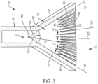
- FIG. 3 details of the inner nodes or ports 44 of input/output waveguides 12, output/input waveguide 14, and transition waveguide 16 are shown.
- An inner port 56 of output/input waveguide 14 contacts side walls 34, 36 of transition waveguide 16.
- Transition waveguide 16 has a cavity 58 extending between inner port 56 of output/input waveguide 14 and inner nodes 44 of input/output waveguides 12.
- the transition waveguide flares outwardly in the E-plane from the inner port of the output/input waveguide toward the inner nodes of the input/output waveguides and communicatively couples the output/input waveguide with the plurality of input/output waveguides.
- the heights H of input/output waveguides 12 at the inner nodes are very small compared to the heights H at the outer nodes 32.
- the tapered walls vary from a small value of thickness T at the inner nodes compared to the thickness T at the outer nodes.
- Fig. 4A is a diagram illustrating idealized E-field magnitude distribution in a cross-section of the output/input waveguide 14 of combiner/divider 10 of Figs. 1-3 .
- Fig. 4B is a diagram illustrating idealized E-field magnitude distribution in a representative cross-section of the inner end 44 of an individual input/output waveguide 12 of combiner/divider 10.
- Fig. 4C is a diagram illustrating a combination of E-field magnitude distributions distributed across representative cross-sections of inner ends 44 of a reduced number (to facilitate illustration) of stacked input/output waveguides 12 of combiner/divider 10 of Figs. 1-3 .
- Fig. 4C thus illustrates that the summation of the E-field distributions of the stacked input/output waveguides corresponds to the E-field distribution in the output/input waveguide as shown in Fig. 4A .
- Radius R1 of cavity 58 may be selected based on size and performance considerations appropriate for a particular application.
- an objective of the combiner/divider is for the multiplicity of the electrical fields that arrive at cavity 58 from input/output waveguides 12 near output/input waveguide 14 (when operating as a combiner) to add up in space as they travel toward the output/input waveguide such that the composite addition of these input electric fields matches the fundamental TE10 mode of the output/input waveguide.
- a conceptually minimum value of radius R1 is a value chosen such that the arc defined by radius R1 intersects the end of output/input waveguide 14 at inner port 56, which is where the angled side walls 34, 36 of the ends of uppermost and bottommost truncated tapered input/output waveguides 12 reach this point. This results in radius R1 being less than a half of a wavelength of a center design frequency.
- the heights H of truncated input/output waveguides 12 at inner nodes 44 would be extremely small and typically would be impractical to manufacture as would the tapered waveguide walls 32, which would become extremely thin at the inner ends proximate cavity 58.
- the input waveguide wall thickness would have to be tapered to near zero thickness, i.e. a razor sharp end at that point.
- the open ends of the input/output waveguides i.e. their apertures
- radius R1 In general, the smaller the value of radius R1, the better the failure mode performance is, but this is extremely difficult to quantify because it depends upon N and radius R1 as well as whether a constant input waveguide wall thickness T is employed (as in combiner/divider 70 of Figs. 5-9 ) or a tapered input waveguide wall thickness T is employed (as in combiner/divider 10 of Figs. 1-3 ).
- Figs. 5-9 illustrate a second embodiment of a combiner/divider that may be designed to operate in the WR975 waveguide frequency band of 0.75 - 1.15 GHz.
- Fig. 5 is an isometric view of an example of a combiner/divider 70 having a plurality of 32 input/output waveguides 72 including integrated input/output coaxial-to-waveguide transitions communicatively coupled to an output/input waveguide 74 by a transition waveguide 76.
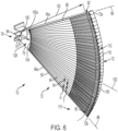
- Fig. 6 is an isometric view of a cross section of combiner/divider 70 taken along a plane of stacked input/output waveguides 72 including integrated input/output coaxial-to-waveguide transitions.
- Fig. 5 is an isometric view of an example of a combiner/divider 70 having a plurality of 32 input/output waveguides 72 including integrated input/output coaxial-to-waveguide transitions communicatively coupled to an output/input waveguide 74 by a transition waveguide 76.
- FIG. 7 is an enlarged isometric view of a portion of combiner/divider 70 in cross section as shown in Fig. 6 showing details of output/input waveguide 74, transition waveguide 76, and truncated inner ends of input/output waveguides 72.
- Fig. 8 is an enlarged isometric view in lengthwise cross section, as in Fig. 6 , of a representative individual input/output waveguide 72 including an integrated input/output coaxial-to-waveguide transition of combiner/divider 70.
- Fig. 9 is a further enlarged image of a distal portion of the input/output waveguide of Fig. 8 having an integrated coaxial-to-waveguide transition.
- Combiner/divider 70 is made of electrically conductive material, such as copper, and has other features generally similar to features of combiner/divider 10 discussed above, so comments about the similar features made with reference to combiner/divider 10 also apply to combiner/divider 70.
- Input/output waveguides 72 are stacked in their E-Planes as was discussed above for input/output waveguides 12. Input/output waveguides 72 and transitional waveguide 76 are positioned in the configuration of a radial sector 78 defined by outer radii 80, 82, that extend from a center 84 along respective radial lines 86, 88, and an arc 90 extending between the outer radii at outer input/output waveguide nodes 92. In this example, outer nodes 92 are also distal input/output ports of input/output waveguides 72. Input/output waveguides 72 are stacked in sector 78 in a plane corresponding to the plane of sector 78 and the plane of cross section in the view of Fig. 6 , which is in the E-planes of the input/output waveguides.
- Arc 90 subtends an angle A of 60 degrees, although other angles may be used as appropriate for a given application and number of input/output waveguides. It is preferable that the input/output waveguides extend at least partially in a common direction away from center 84. With combiner/divider 70 each of input/output waveguides 72 extend at least partially to the right as viewed in Figs. 5 and 6 .
- Outer side walls 94a, 96a extend from output/input waveguide 74 along respective radial lines 86, 88, and thereby also along respective sector radii 80, 82, to arc 90.
- Outer side walls 94a, 96a are the outer sides of combiner/divider 70 and also the upper side wall of a top input/output waveguide 72a and a lower side wall of a bottom input/output waveguide 72b, respectively.
- each input/output waveguide 72 has an upper side wall 94 and an opposite lower side wall 96, and also has opposite face plates 98, 100 that extend parallel to the plane of sector 78 between respective individual side walls 94, 96.
- Side walls 94, 96 are seen to be transverse, such as perpendicular, to the plane of sector 78.
- Side walls 94, 96 and face plates 98, 100 thereby have inner-facing surfaces that form input/output waveguides 72.
- Outer side walls 94a, 96a also are side walls of output/input waveguide 74 and transition waveguide 76.
- Face plates 98a, 100a extend parallel to the plane of sector 78 between side walls 94a, 96a of output/input waveguide 74 and transition waveguide 76.
- input/output waveguides 72 extend along respective radial lines, such as radial line 102, extending from center 84 within sector 78. All of the input/output waveguides are of equal dimensions providing equal phase and amplitude of signals guided by the input/output waveguides.
- Each input/output waveguide 72 has a height H in the E-plane that is transverse to the length of the input/output waveguide. Height H varies along the lengths of the input/output waveguides between inner nodes 104 and outer nodes 92.
- Inner nodes 104 are aligned in an arc having a radius R1 and outer nodes 92 along arc 90 are located at a radius R2 from center 84.
- each of the tapered waveguides is thus the difference between radii R1 and R2.
- waveguide height H increases linearly from inner node 104 to outer node 92, but could also increase in a nonlinear fashion as appropriate for a particular application.
- input/output waveguides 72 could extend further and have other configurations, as mentioned above for combiner/divider 10. For example, there could be a section that extends beyond nodes 92 in which the heights of the input/output waveguides are constant.
- the input/output waveguides have wall faces defining the waveguides, such as face 106 of transverse wall 94 and face 108 of transverse wall 96. Faces 106 and 108 are transverse to the plane of sector 78.
- the heights H of the input/output waveguides increases more than those of combiner/divider 10 for a given length of waveguide for a sector of a given sector angle A.
- the input/output waveguide walls of constant thickness thus result in increased amounts of waveguide taper per length of for a given sector angle, which correspondingly results in a more compact structure size for combiner/divider 70.
- integrated end-launch coaxial-to-waveguide transitions 110 are mounted proximate to outer nodes 92 of input/output waveguides 72.
- Coaxial-to-waveguide transitions 110 transition input/output waveguides 72 to coaxial transmission line connectors 112.
- the coaxial-to-waveguide transitions include coaxial center conductors 114 that extend from the center of coaxial connector 112 into the centers of input/output waveguides 72.
- the center conductors extend in tapered input/output waveguides 72 from outer nodes 92 toward inner nodes 104.
- Coaxial connectors 112 are mounted in end plates 116 that cover the waveguide ports at nodes 92.
- the coaxial connectors have outer shield conductors 118 that are connected to end plates 116 and electrically and physically spaced from the center conductors by dielectric insulators 120.
- the center conductors extend from the coaxial connectors to distal ends that are typically a quarter guide-wavelength of a center design frequency from the coaxial connectors.
- the distal ends are supported by conductive waveguide probes 122 connecting the distal ends of the center conductors to the bottom walls 96 of the input/output waveguides.
- electrically conductive tuning discs 124 are attached to walls 94 opposite probes 122. It will be appreciated that other configurations of coaxial-to-waveguide transitions may also be used for applications where input/output waveguides 72 transition to coaxial transmission lines.
- FIG. 7 details of the inner nodes or ports 104 of input/output waveguides 72, output/input waveguide 74, and transition waveguide 76 are shown.
- An inner port 126 of output/input waveguide 74 contacts side walls 94a, 96a of transition waveguide 76.
- Transition waveguide 76 has a cavity 128 extending between inner port 126 of output/input waveguide 74 and inner nodes 104 of input/output waveguides 72.
- the transition waveguide flares outwardly in the E-plane from the inner port of the output/input waveguide toward the inner nodes of the input/output waveguides and communicatively couples the output/input waveguide with the plurality of input/output waveguides.
- the heights H of input/output waveguides 72 at the inner nodes are very small compared to the heights H at the outer nodes 92.
- the combination of adjacent walls 94 and 96 between input/output waveguides are a constant thickness T along the full length of the input/output waveguides between the inner nodes and the outer nodes.
- the combiner/divider design structure shown in the figures herein employs tapered input waveguides such that their heights are all equal where they are truncated near the radial sector origin. This yields equal amplitude coupling between each input/output waveguide port and the output/input waveguide when used as a combiner.
- the structure is used as a power divider to provide signals to radiating elements in an array antenna in order to achieve low sidelobes in the radiation pattern of an array antenna it is desirable to provide larger signals to the central array elements and the signals should decrease toward the ends of the array.
- the signal distribution can be a truncated Gaussian or a Taylor distribution, for example.
- the tapered waveguides may be designed to have larger heights for the central ports and decreasing heights for the end or outer ports where they are truncated at the transition waveguide. In such embodiments and depending on the application, some of the input/output waveguides may not be tapered.
- a wider frequency band of operation may be realized using single or double-ridged waveguides.
- the cross sections of the waveguides shown in the figures herein are rectangular.
- the frequency bandwidth for such waveguides is in a range from just above the cutoff frequency of the lowest order mode (TE 10 ) and just below the cutoff frequency of the next higher order mode (TE 20 ) mode. This typically provides a bandwidth of approximately 36%.
- TE 10 lowest order mode
- TE 20 next higher order mode
- the sector angle and rate of waveguide taper per length of input/output waveguide may be varied from those shown.
- the waveguide impedances decrease linearly as a function of distance from the outer nodes in the examples shown. Rates of taper other than linear have differing performance characteristics. As such, the longer they are the more gradual the impedance taper is and the better the VSWR is.
- input/output waveguides 72 shown in Figs. 1-3 may be made half height WR159 to keep the size of the combiner smaller. If full height input/output waveguides are employed, then the combiner/divider would be approximately twice the length and width. The length of the waveguide may thus be selected so that the taper is sufficiently gradual that very good VSWR performance is achieved.
- the embodiments shown have single sectors for both the transition waveguide and the input/output waveguides. In some examples, different sector angles may be used. Additionally, the input/output waveguides may extend along different sectors along their lengths. In general, then, other sector configurations may also be realized. However, if the requirement is to add all inputs with equal amplitude and phase weights as is specified for most combiner designs, then sector segments with different subtended angles would cause the input signals to be combined with unequal weights, which is usually undesirable.
- the different embodiments of the combiner/divider described herein provide several advantages over known solutions for dividing or combining high power RF frequency signals.
- the illustrative embodiments of combiner/dividers described herein allow high power signals to be combined or divided at low loss.
- As a combiner it is configured to efficiently combine a plurality of input signals directly to an input port of an output waveguide.
- the resultant power combiner's output power level capability can approach that of the output waveguide.
- not all embodiments described herein provide the same advantages or the same degree of advantage. Variations of these embodiments may also have different advantages or different degrees of advantage.
- the disclosed embodiments do not require a coaxial transmission line divider or combiner section at the input/output port which exhibit substantially lower peak and average power handling and thus provides high output power capability.
- Such a design employs waveguide input ports and a structure that efficiently combines all the input signals directly to a waveguide output/input port with no intermediate coaxial transmission line necessary. This is in contrast to radial waveguide power combiner/dividers which include coaxial output/input sections which limit their power handling capability.
- a plurality of input/output waveguides are stacked in their E-Planes within a radial sector and taper in height moving from their input/output ports at the outer nodes toward the output/input waveguide where the signals from all the input/output waveguides are added to produce extremely high output power when used as a combiner. Furthermore, since the structure is reciprocal, it may be operated in reverse as a power divider wherein the input/output waveguides function as output waveguides and the output/input waveguide functions as an input waveguide.
- N when used as a combiner or output ports, N, when used as a divider, does not have to be a power of 2, i.e. N does not need to be a binary number, it may be any positive integer greater than or equal to 2.
- N does not need to be a binary number, it may be any positive integer greater than or equal to 2.
- This is an advantage when the subject invention is compared to any so-called corporate network arrangements consisting of a multiplicity of 2-way combiners/dividers (typically Magic-Ts) with N inputs/outputs for which N would necessarily be constrained to be a binary number. This binary-number constraint clearly limits system design flexibility.
- ordinal indicators such as first, second, or third, for identified elements are used to distinguish between the elements in the order in which they are introduced, and do not indicate a required or limited number of such elements, and do not indicate a particular position or order of such elements unless otherwise specifically indicated. Accordingly, the ordinal indicator used for a particular element may vary in different contexts.
Landscapes
- Waveguides (AREA)
Description
- The present disclosure relates generally to power combiners/dividers in radio frequency (RF) devices, and specifically to N-Way waveguide or coaxial power combiners/dividers.
- When it is desirable to combine many high-power input signals to achieve an extremely high-power output signal with very low-loss, 360-degree radial waveguide power combiners are typically employed. Such radial waveguide power combiners may typically incorporate waveguide or coaxial input port geometries. The input signals are then combined in the center of the radial waveguide by a transition from radial waveguide to a transverse electro-magnetic (TEM) mode coaxial transmission line. The coaxial transmission line is utilized because of its circular symmetry to achieve a high degree of amplitude and phase balance of the input signals for efficient combining. The coaxial transmission line must operate in its lowest order (TEM) mode in order to maintain amplitude and phase balance. This necessitates the cross-sectional dimensions of the coaxial transmission line to be below a threshold which depends upon the operating frequency range in order to render any undesirable higher order modes evanescent by decaying sufficiently to avoid perturbing the amplitude and phase balance. Invoking this cross-sectional dimension constraint on the coaxial transmission line limits both the peak and average power levels that can be achieved without component failure.
-
U.S. Patent Number 3,218,580 A issued to Zanichkowsky discloses a waveguide power divider for channeling an electromagnetic wave to a plurality of energy receivers such as radiating antennas and the like. A waveguide element has sidewalls and a top and a bottom wall. The latter two walls flare away from each other in the fashion of a horn while the sidewalls remain parallel to each other. A plurality of power dividing walls are located between the top and the bottom walls of the waveguide element. The number of walls depends on the number of outputs into which the incoming electromagnetic wave is to be divided. The arrangement is further characterized in that each waveguide channel at the output end of the element is provided with a dielectric vane which can be adjustably positioned to select a desired phase shift in the electromagnetic wave carried by that channel. -
U.S. Patent Number 4,599,584 A issued to Sasser et al. discloses a power divider/combiner apparatus comprising a fan shaped waveguide. A generally fan shaped electrically conducting base member defines a waveguide cavity with a waveguide input/output in communication with the cavity at the apex thereof and a plurality of output/input waveguides in communication with the cavity equal angularly spaced along the arc of the base member. The inputs and outputs are formed in the plane of the cavity so that losses are substantially reduced and all of the output/input waveguides are equally spaced along radii of the base member and are of equal length so that signals at the outlets thereof are of equal amplitude and phase without requiring phase shifters and the like. U.S. patent NumberUS 4 947 143 A discloses a multi-port power divider-combiner comprising an arrangement having an arcuate boundary region of substantially constant radius. A first port is disposed substantially at the center of the curvature of the arcurate boundary region and lies at the boundary of the arrangement and in electrical communication with it. A plurality of second ports are disposed around the arcuate boundary region and in electrical communication with it. It also discloses that these power divider-combiner circuits may be cascaded in a fan-out or a fan-in manner. - A combiner/divider is set out in the appended set of claims.
- Features, functions, and advantages may be achieved independently in various embodiments of the present disclosure, or may be combined in yet other embodiments, further details of which can be seen with reference to the following description and drawings.
- Additional aspects of combiners/dividers will become evident upon reviewing the non-limiting embodiments described in the description and the claims taken in conjunction with the accompanying figures, in which:
-
Fig. 1 is an isometric view of an example of a 16-Way combiner/divider having 16 tapered input/output waveguides stacked in their E-Planes within a radial sector structure; -
Fig. 2 is a cross-section of the combiner/divider ofFig. 1 taken along a plane containing the 16 input/output waveguides; -
Fig. 3 is an enlarged isometric view of a portion of the combiner/divider in cross section as shown inFig. 2 showing details of an output/input waveguide, transition waveguide, and truncated inner ends of the input/output waveguides; -
Fig. 4A is a diagram illustrating electric (E)-field magnitude distribution in a cross-section of the output/input waveguide of the combiner/divider ofFigs. 1-3 ; -
Fig. 4B is a diagram illustrating E-field magnitude distribution in a representative cross-section of the inner end of an input/output waveguide of the combiner/divider ofFigs. 1-3 ; -
Fig. 4C is a diagram illustrating E-field magnitude distribution in representative cross-sections of the inner ends of stacked input/output waveguides of the combiner/divider ofFigs. 1-3 illustrating that the summation of the E-field distributions of the individual stacked input/output waveguides corresponds to the E-field distribution in the output/input waveguide as shown inFig. 4A ; -
Fig. 5 is an isometric view of an example of a combiner/divider having 32 input/output waveguides stacked in their E-Planes with waveguide walls of constant thickness and integrated coaxial-to-waveguide transitions on the distal ends of the input/output waveguides; -
Fig. 6 is an isometric view of a cross section of the combiner/divider ofFig. 5 taken along a plane of the stacked input/output waveguides; -
Fig. 7 is an enlarged isometric view of a portion of the combiner/divider in cross section as shown inFig. 6 showing details of an output/input waveguide, transition waveguide, and inner ends of the input/output waveguides; -
Fig. 8 is an enlarged isometric view in lengthwise cross section of a representative individual input/output waveguide of the combiner/divider ofFig. 5 ; and -
Fig. 9 is a further enlarged image of a portion of the input/output waveguide ofFig. 8 showing the coaxial-to-waveguide transition in more detail. - Various embodiments of a combiner/divider coupling a plurality of input/output waveguides to an output/input waveguide are described below and illustrated in the associated drawings. Unless otherwise specified, a combiner/divider and/or its various components may, but is not required to, contain at least one of the structure, components, functionality, and/or variations described, illustrated, and/or incorporated herein. Furthermore, the structures, components, functionalities, and/or variations described, illustrated, and/or incorporated herein may, but are not required to, be included in other combiners and/or dividers. The following description of various embodiments is merely exemplary in nature and is in no way intended to limit its scope, applications, or uses. Additionally, the advantages provided by the embodiments, as described below, are illustrative in nature and not all embodiments provide the same advantages or the same degree of advantages.
- Generally, a combiner/divider as disclosed herein includes a transition waveguide interposed between a plurality of input/output waveguides and an output/input waveguide. In applications where the input/output waveguides are the same and are distributed in a radial sector extending in the E-plane of the input/output waveguides, equal amplitude and phase signals are propagated in the input/output waveguides. It will be appreciated that other configurations may be realized for other applications for providing the same or different signal amplitudes and phases. The input/output waveguides extend from inner nodes disposed proximate to and spaced from a sector center to outer nodes disposed along an arc of the sector. Again, depending on the application, at least some of the input/output waveguides taper in size between the inner nodes and the outer nodes. Walls between adjacent input/output waveguides also may taper in width between the inner nodes and the outer nodes. It will be appreciated that the rate of taper of the waveguides and/or walls as well as sizes of the waveguides at the inner and outer nodes affect the overall size of the combiner/divider. In general, the output/input waveguide has an inner port facing and spaced from the inner nodes of the input/output waveguides. A transition waveguide extends between the input/output waveguides and the output/input waveguide and has side walls extending along the radii of the sector for communicatively coupling the output/input waveguide with the input/output waveguides.
- The structures disclosed herein may be used as either combiners or dividers. The general term "combiner/divider" identifies both functions, with the applicable function depending on the use of the structure. When used as a combiner, then input/output waveguides function as input waveguides, and an output/input waveguide functions as an output waveguide. Correspondingly, when used as a divider, the output/input waveguide functions as an input waveguide and the input/output waveguides function as output waveguides.
- "Sector" refers to a geometrical figure bounded by two equal-length outer radii extending from a common center and an included arc of a circle connecting outer ends of the outer radii.
- "Node" refers to a point on an electrical circuit where a characteristic of the circuit may be identified. A port or a terminal is considered a node of a circuit structure that provides external access or represents an end of a circuit component or structure, such as a waveguide.
- The following sections describe selected aspects of exemplary combiner/dividers. The examples in these sections are intended for illustration and should not be interpreted as limiting the entire scope of the underlying concepts. Each section may include one or more distinct inventions, and/or contextual or related information, function, and/or structure.
- Referring initially to
Figs. 1-3 , a combiner/divider is disclosed that can be used to guide high power signals at low loss. As a combiner it is configured to efficiently combine a plurality of input signals directly to an input port of an output waveguide. The resultant power combiner's output power level capability can approach that of the output waveguide. This is typically orders of magnitude greater than the maximum power that could be achieved in designs that incorporate coaxial transmission line sections such as radial waveguide power combiners. For example, for the rectangular waveguide WR159 recommended waveguide frequency band of 4.9-7.05 GHz, the peak power handling is 2.79 Mw and the average power handling is 15 Kw using copper waveguide material. A plurality of input/output waveguides are stacked in their E-Planes within a radial sector and taper down in height from the input/output ports of the input/output waveguides toward the output/input waveguide where the signals from all the input/output waveguides are added to produce extremely high output power when operating in a combiner mode. This combiner design structure is more compact and lower-loss than other high-power waveguide combiner/divider designs which, for example, are comprised of a multiplicity of cascaded "Magic-T" 2-way waveguide combiner/dividers in a corporate arrangement. - In the example embodiment shown in
Figs. 1-3 , an equal amplitude and phase 16-Way combiner/divider has sixteen waveguide input/output ports positioned on a circular arc within a radial sector of subtended angle A. Any practical number, N, of input/output waveguides can be employed and N can be any appropriate positive integer greater than or equal to 2, i.e. N does not have to be a power of 2. The input/output waveguides are spaced on a circular arc such that there is sufficient area around each input/output waveguide port for connection to the waveguide flange of an external input/output device, such as an amplifier. Alternatively, if coaxial inputs/outputs are preferred for a particular embodiment as shown inFigs. 5-9 , then end-launch coaxial-to-waveguide transitions may be employed and these can be connected to the areas around each input/output waveguide port. The central axes of the input waveguides are oriented such that they are normal to the circular arc of the radial sector. These input/output waveguide axes intersect at the center or origin of the radial sector near the location of the output/input waveguide. - When operating in the combiner mode, the input waveguides are tapered in their heights and continue to be reduced in their heights until they arrive close to the origin of the radial sector near the location of the output waveguide, i.e. in a cavity region at the inner ends of the input waveguides. The tapered input waveguides are at their minimum heights at their ends close to the origin of the radial sector where the top and bottom walls of the input waveguides are truncated. The input waveguides radiate into the cavity region between their truncated ends and the output waveguide. If all the input waveguides have input signals that are equal in amplitude and in-phase, then when these signals arrive at the truncated inner ends of the input waveguides the radiated electric fields from each of them constructively add and form a composite electric field distribution which closely matches the electric field distribution required in the output waveguide so that any reflections are low. Any small reflections can easily be compensated by the inclusion of small scattering objects (not shown in the figures), such as posts, known to those skilled in the art.
- It should be noted that the top and bottom waveguide walls of the input/output waveguides are preferably tapered in their thicknesses to achieve a compact design and also to reduce the sizes of their truncated inner ends. This allows the E-fields of the truncated input waveguides to provide a more continuously uniform E-field distribution to closely match the preferred uniform e-field distribution of the output/input waveguide. However, for lower frequencies, the input/output waveguide walls may be constant in thickness preferably as long as the thickness is a very small portion of a wavelength.
- Specifically,
Figs. 1-3 illustrate a combiner/divider 10 made of electrically conductive material, such as copper, and having a plurality of input/output waveguides 12. In this example, there are sixteen input/output waveguides 12, although any suitable number of waveguides may be used subject to manufacturing tolerances. Input/output waveguides 12 are communicatively coupled to an output/input waveguide 14 via atransitional waveguide 16. - Input/
output waveguides 12 andtransitional waveguide 16 are positioned in the configuration of aradial sector 18 defined byouter radii center 24 alongrespective radial lines 26, 28, and anarc 30 extending between the outer radii at outer input/output waveguide nodes 32. In this example,outer nodes 32 are also distal input/output ports of input/output waveguides 12. The input/output waveguides are stacked insector 18 in a plane corresponding to the plane ofsector 18 and the plane of view ofFig. 2 , which is in the E-planes of the input/output waveguides. -
Arc 30 subtends an angle A of 60 degrees, although other angles may be used as appropriate for a given application and number of input/output waveguides. It is preferable that the input/output waveguides extending from acenter 24 extend at least partially in a common direction. With combiner/divider 10, each of input/output waveguides 12 extend at least partially to the right as viewed inFig. 2 . - A subtended angle of 60 degrees is found to provide a good compromise between a very small subtended angle which would require a very long structure to accommodate the width of the input/output nodes 32 (either waveguides or coaxial connectors) and a larger subtended angle for which the input waves from the uppermost and lowermost input/
output waveguides 12 would arrive at the aperture (inner port) of output/input waveguide 14 approaching a "sideways" incident condition (which would occur at the extreme value of 180 degree subtended angle). This could cause the coupling of end input/output waveguides 12 to output/input waveguide 14 to be weaker than the central ones and that would degrade amplitude balance. The advantage of large subtended angles is the reduction of the length of the combiner for a given number of input/output waveguides. A sector angle of 60 degrees thus provides a balance of combiner length and electrical performance, depending on the number of input/output waveguides that are being combined. That being said, the subtended angle could be anywhere from a very small angle approaching 0 degrees to an angle approaching 180 degrees. -
Side walls input waveguide 14 alongrespective radial lines 26, 28 toarc 30. Oppositeface plates sector 18 betweenside walls side walls face plates output waveguides 12, output/input waveguide 14, andtransition waveguide 16. - In this example, input/
output waveguides 12 extend along respective radial lines, such asradial line 42, extending fromcenter 24. All of the input/output waveguides are of equal dimensions providing equal phase and amplitude of signals guided by the input/output waveguides. As shown particularly inFig. 2 , each input/output waveguide 12 has a height H in the E-plane that is transverse to the length of the input/output waveguide. Height H varies along the lengths of the input/output waveguides betweeninner nodes 44 andouter nodes 32.Inner nodes 44 are aligned in an arc having a radius R1 andouter nodes 32 alongarc 30 are located at a radius R2 fromcenter 24. The length of the tapered waveguides is thus the difference between radii R1 and R2. Specifically, waveguide height H increases linearly frominner node 44 toouter node 32. It will be appreciated that beyondinner nodes 44 andouter nodes 32, input/output waveguides 12 could extend further and have other configurations. For example, there could be asection 46 of combiner/divider 10 that extends beyondarc 30 in which the heights of the input/output waveguides are constant, as illustrated by a fragmentary portion shown in dashed lines. - In combiner/
divider 10, input/output waveguides 12 typically vary continuously linearly betweeninner nodes 44 andouter nodes 32, but may also vary in a nonlinear fashion, such as exponentially. The input/output waveguides may have wall faces defining the waveguides, such as faces 48 oftransverse walls 50 that are transverse to the plane ofsector 18 and extend along radial lines, such asradial line 52, along the lengths of the input/output waveguides betweeninner nodes 44 andouter nodes 32. As mentioned, the heights of the input/output waveguides can vary linearly or nonlinearly along their lengths. As a result, the thicknesses T of the walls separating the input/output waveguides also increases linearly frominner nodes 44 toouter nodes 32. Generally, the wall thicknesses will be the result of a desired design in the configurations of the input/output waveguides. As will be seen with the combiner/divider illustrated inFigs. 5-9 , waveguide walls of constant thickness increase the amount of taper available for the waveguides for a given sector angle, which results in a more compact structure size. - Referring to
Fig. 3 , details of the inner nodes orports 44 of input/output waveguides 12, output/input waveguide 14, andtransition waveguide 16 are shown. Aninner port 56 of output/input waveguide 14contacts side walls transition waveguide 16.Transition waveguide 16 has acavity 58 extending betweeninner port 56 of output/input waveguide 14 andinner nodes 44 of input/output waveguides 12. The transition waveguide flares outwardly in the E-plane from the inner port of the output/input waveguide toward the inner nodes of the input/output waveguides and communicatively couples the output/input waveguide with the plurality of input/output waveguides. It is seen that the heights H of input/output waveguides 12 at the inner nodes are very small compared to the heights H at theouter nodes 32. Similarly, the tapered walls vary from a small value of thickness T at the inner nodes compared to the thickness T at the outer nodes. -
Fig. 4A is a diagram illustrating idealized E-field magnitude distribution in a cross-section of the output/input waveguide 14 of combiner/divider 10 ofFigs. 1-3 .Fig. 4B is a diagram illustrating idealized E-field magnitude distribution in a representative cross-section of theinner end 44 of an individual input/output waveguide 12 of combiner/divider 10.Fig. 4C , then, is a diagram illustrating a combination of E-field magnitude distributions distributed across representative cross-sections of inner ends 44 of a reduced number (to facilitate illustration) of stacked input/output waveguides 12 of combiner/divider 10 ofFigs. 1-3 .Fig. 4C thus illustrates that the summation of the E-field distributions of the stacked input/output waveguides corresponds to the E-field distribution in the output/input waveguide as shown inFig. 4A . - Radius R1 of
cavity 58 may be selected based on size and performance considerations appropriate for a particular application. AsFigs 4A-4C illustrate, an objective of the combiner/divider is for the multiplicity of the electrical fields that arrive atcavity 58 from input/output waveguides 12 near output/input waveguide 14 (when operating as a combiner) to add up in space as they travel toward the output/input waveguide such that the composite addition of these input electric fields matches the fundamental TE10 mode of the output/input waveguide. - A conceptually minimum value of radius R1, such as radius R1' shown in dashed lines in
Fig. 3 , is a value chosen such that the arc defined by radius R1 intersects the end of output/input waveguide 14 atinner port 56, which is where theangled side walls output waveguides 12 reach this point. This results in radius R1 being less than a half of a wavelength of a center design frequency. However, if this was done, the heights H of truncated input/output waveguides 12 atinner nodes 44 would be extremely small and typically would be impractical to manufacture as would the taperedwaveguide walls 32, which would become extremely thin at the inner endsproximate cavity 58. - Even if the frequency was low enough such that the truncated ends of the input/output waveguides at
inner nodes 44 could be manufactured to reach the location of radius R1', where the uppermost and bottommost truncated tapered input waveguides reach the end of the output/input waveguide atinner port 56, the input waveguide wall thickness would have to be tapered to near zero thickness, i.e. a razor sharp end at that point. Furthermore, the open ends of the input/output waveguides (i.e. their apertures) would act like an array of slot antennas as would the internal sides of the output/input waveguide. When antennas are moved close enough to be in each other's near fields, there would be interactions in the form of reflections back and forth between the array of input/output waveguide slots and the internal aperture of the output/input waveguide. Although these interactions can be compensated for by cancelling reflections from an impedance matching structure (like ribs in the output/input waveguide), it is generally more practical to keep a slightly greater value for R1 to reduce such interactions. - Since very good performance can be achieved with radius R1 significantly larger than this minimal value, such as two to three times greater than the minimum value, it is not necessary to make the manufacturing so onerous for conventional manufacturing processes.
- The previous statement applies when considering the voltage standing-wave ratio (VSWR), amplitude, and phase balance of combiner/
divider 10. A much more complex performance aspect is the effect on performance if one of the input amplifiers fails and also if a "hot-swap" feature is required, i.e. the failure-mode performance. "Hot-Swap" means that when an input amplifier fails, it can be removed and replaced while all the other amplifiers remain operational. To determine the VSWR under the conditions of an amplifier failing and also when it is removed for "Hot-Swap", requires the calculation of the (N+ 1)×(N+ 1) S-matrix (scattering matrix) for a combiner with N input ports. In general, the smaller the value of radius R1, the better the failure mode performance is, but this is extremely difficult to quantify because it depends upon N and radius R1 as well as whether a constant input waveguide wall thickness T is employed (as in combiner/divider 70 ofFigs. 5-9 ) or a tapered input waveguide wall thickness T is employed (as in combiner/divider 10 ofFigs. 1-3 ). - Notwithstanding the above, for example, very good performance is achieved for combiner/
divider 10 ofFigs. 1-3 with radius R1 approximately equal to 1.2 wavelengths at a center frequency of a design frequency band. If there is not a requirement for failure mode performance, i.e. if it is acceptable for the combiner/divider to operate with good performance when all amplifiers are working. Radius R1 may be much greater than the minimum in such a case, but since a very large radius R1 defines a verylarge cavity 58, in the event of imbalances in the input amplifiers' signals (either in their amplitude or phase), high order modes are excited in the cavity, resulting in degraded performance. A combiner/divider -
Figs. 5-9 illustrate a second embodiment of a combiner/divider that may be designed to operate in the WR975 waveguide frequency band of 0.75 - 1.15 GHz.Fig. 5 is an isometric view of an example of a combiner/divider 70 having a plurality of 32 input/output waveguides 72 including integrated input/output coaxial-to-waveguide transitions communicatively coupled to an output/input waveguide 74 by atransition waveguide 76.Fig. 6 is an isometric view of a cross section of combiner/divider 70 taken along a plane of stacked input/output waveguides 72 including integrated input/output coaxial-to-waveguide transitions.Fig. 7 is an enlarged isometric view of a portion of combiner/divider 70 in cross section as shown inFig. 6 showing details of output/input waveguide 74,transition waveguide 76, and truncated inner ends of input/output waveguides 72.Fig. 8 is an enlarged isometric view in lengthwise cross section, as inFig. 6 , of a representative individual input/output waveguide 72 including an integrated input/output coaxial-to-waveguide transition of combiner/divider 70.Fig. 9 is a further enlarged image of a distal portion of the input/output waveguide ofFig. 8 having an integrated coaxial-to-waveguide transition. Combiner/divider 70 is made of electrically conductive material, such as copper, and has other features generally similar to features of combiner/divider 10 discussed above, so comments about the similar features made with reference to combiner/divider 10 also apply to combiner/divider 70. - Input/
output waveguides 72 are stacked in their E-Planes as was discussed above for input/output waveguides 12. Input/output waveguides 72 andtransitional waveguide 76 are positioned in the configuration of aradial sector 78 defined byouter radii center 84 alongrespective radial lines arc 90 extending between the outer radii at outer input/output waveguide nodes 92. In this example,outer nodes 92 are also distal input/output ports of input/output waveguides 72. Input/output waveguides 72 are stacked insector 78 in a plane corresponding to the plane ofsector 78 and the plane of cross section in the view ofFig. 6 , which is in the E-planes of the input/output waveguides. -
Arc 90 subtends an angle A of 60 degrees, although other angles may be used as appropriate for a given application and number of input/output waveguides. It is preferable that the input/output waveguides extend at least partially in a common direction away fromcenter 84. With combiner/divider 70 each of input/output waveguides 72 extend at least partially to the right as viewed inFigs. 5 and6 . -
Outer side walls input waveguide 74 alongrespective radial lines arc 90.Outer side walls divider 70 and also the upper side wall of a top input/output waveguide 72a and a lower side wall of a bottom input/output waveguide 72b, respectively. As shown particularly inFigs. 8 and9 , each input/output waveguide 72 has anupper side wall 94 and an oppositelower side wall 96, and also hasopposite face plates sector 78 between respectiveindividual side walls Side walls sector 78.Side walls face plates output waveguides 72. -
Outer side walls input waveguide 74 andtransition waveguide 76.Face plates sector 78 betweenside walls input waveguide 74 andtransition waveguide 76. - In this example, input/
output waveguides 72 extend along respective radial lines, such asradial line 102, extending fromcenter 84 withinsector 78. All of the input/output waveguides are of equal dimensions providing equal phase and amplitude of signals guided by the input/output waveguides. Each input/output waveguide 72 has a height H in the E-plane that is transverse to the length of the input/output waveguide. Height H varies along the lengths of the input/output waveguides betweeninner nodes 104 andouter nodes 92.Inner nodes 104 are aligned in an arc having a radius R1 andouter nodes 92 alongarc 90 are located at a radius R2 fromcenter 84. The length of each of the tapered waveguides is thus the difference between radii R1 and R2. Specifically, waveguide height H increases linearly frominner node 104 toouter node 92, but could also increase in a nonlinear fashion as appropriate for a particular application. It will be appreciated that beyondinner nodes 104 andouter nodes 92, input/output waveguides 72 could extend further and have other configurations, as mentioned above for combiner/divider 10. For example, there could be a section that extends beyondnodes 92 in which the heights of the input/output waveguides are constant. - The input/output waveguides have wall faces defining the waveguides, such as
face 106 oftransverse wall 94 and face 108 oftransverse wall 96.Faces sector 78. In combiner/divider 70 the wall thicknesses T/2 are constant over the lengths of the input/output waveguides. Since there are two walls between waveguide-defining wall faces, the total wall thickness between waveguides is T/2 + T/2 = T. As a result, the heights H of the input/output waveguides increases more than those of combiner/divider 10 for a given length of waveguide for a sector of a given sector angle A. The input/output waveguide walls of constant thickness thus result in increased amounts of waveguide taper per length of for a given sector angle, which correspondingly results in a more compact structure size for combiner/divider 70. - As is particularly shown in
Figs. 8 and9 , integrated end-launch coaxial-to-waveguide transitions 110 are mounted proximate toouter nodes 92 of input/output waveguides 72. Coaxial-to-waveguide transitions 110 transition input/output waveguides 72 to coaxialtransmission line connectors 112. The coaxial-to-waveguide transitions includecoaxial center conductors 114 that extend from the center ofcoaxial connector 112 into the centers of input/output waveguides 72. The center conductors extend in tapered input/output waveguides 72 fromouter nodes 92 towardinner nodes 104. -
Coaxial connectors 112 are mounted inend plates 116 that cover the waveguide ports atnodes 92. The coaxial connectors haveouter shield conductors 118 that are connected to endplates 116 and electrically and physically spaced from the center conductors bydielectric insulators 120. The center conductors extend from the coaxial connectors to distal ends that are typically a quarter guide-wavelength of a center design frequency from the coaxial connectors. The distal ends are supported by conductive waveguide probes 122 connecting the distal ends of the center conductors to thebottom walls 96 of the input/output waveguides. In this example, electricallyconductive tuning discs 124 are attached towalls 94opposite probes 122. It will be appreciated that other configurations of coaxial-to-waveguide transitions may also be used for applications where input/output waveguides 72 transition to coaxial transmission lines. - Referring again to
Fig. 7 , details of the inner nodes orports 104 of input/output waveguides 72, output/input waveguide 74, andtransition waveguide 76 are shown. Aninner port 126 of output/input waveguide 74contacts side walls transition waveguide 76.Transition waveguide 76 has acavity 128 extending betweeninner port 126 of output/input waveguide 74 andinner nodes 104 of input/output waveguides 72. The transition waveguide flares outwardly in the E-plane from the inner port of the output/input waveguide toward the inner nodes of the input/output waveguides and communicatively couples the output/input waveguide with the plurality of input/output waveguides. It is seen that the heights H of input/output waveguides 72 at the inner nodes are very small compared to the heights H at theouter nodes 92. However, the combination ofadjacent walls - Variations in the combiner/dividers described above may also be realized. The combiner/divider design structure shown in the figures herein employs tapered input waveguides such that their heights are all equal where they are truncated near the radial sector origin. This yields equal amplitude coupling between each input/output waveguide port and the output/input waveguide when used as a combiner.
- There are some power combiner/divider applications where it is desirable to have an unequal amplitude coupling between the output/input waveguide and the plurality of input/output waveguides. For example, if the structure is used as a power divider to provide signals to radiating elements in an array antenna in order to achieve low sidelobes in the radiation pattern of an array antenna it is desirable to provide larger signals to the central array elements and the signals should decrease toward the ends of the array. The signal distribution can be a truncated Gaussian or a Taylor distribution, for example. Hence, if the subject design structure is used as a divider for this application, then the tapered waveguides may be designed to have larger heights for the central ports and decreasing heights for the end or outer ports where they are truncated at the transition waveguide. In such embodiments and depending on the application, some of the input/output waveguides may not be tapered.
- A wider frequency band of operation may be realized using single or double-ridged waveguides. The cross sections of the waveguides shown in the figures herein are rectangular. The frequency bandwidth for such waveguides is in a range from just above the cutoff frequency of the lowest order mode (TE10) and just below the cutoff frequency of the next higher order mode (TE20) mode. This typically provides a bandwidth of approximately 36%. Using single or double ridged waveguide cross sections, as are known in the art, can substantially increase the operating bandwidth.
- It will be appreciated that the sector angle and rate of waveguide taper per length of input/output waveguide may be varied from those shown. As the heights of the waveguides taper from the outer nodes toward the inner nodes, the waveguide impedances decrease linearly as a function of distance from the outer nodes in the examples shown. Rates of taper other than linear have differing performance characteristics. As such, the longer they are the more gradual the impedance taper is and the better the VSWR is. For example, input/
output waveguides 72 shown inFigs. 1-3 may be made half height WR159 to keep the size of the combiner smaller. If full height input/output waveguides are employed, then the combiner/divider would be approximately twice the length and width. The length of the waveguide may thus be selected so that the taper is sufficiently gradual that very good VSWR performance is achieved. - The embodiments shown have single sectors for both the transition waveguide and the input/output waveguides. In some examples, different sector angles may be used. Additionally, the input/output waveguides may extend along different sectors along their lengths. In general, then, other sector configurations may also be realized. However, if the requirement is to add all inputs with equal amplitude and phase weights as is specified for most combiner designs, then sector segments with different subtended angles would cause the input signals to be combined with unequal weights, which is usually undesirable.
- There are some requirements for unequal amplitude weights combining or dividing as discussed above. Separate sectors with different subtended angles may be useful if it is required that groups of inputs should have different amplitude weights, but this typically is a rare requirement and the design can compensate for phase weight variations.
- The different embodiments of the combiner/divider described herein provide several advantages over known solutions for dividing or combining high power RF frequency signals. For example, the illustrative embodiments of combiner/dividers described herein allow high power signals to be combined or divided at low loss. As a combiner it is configured to efficiently combine a plurality of input signals directly to an input port of an output waveguide. The resultant power combiner's output power level capability can approach that of the output waveguide. However, not all embodiments described herein provide the same advantages or the same degree of advantage. Variations of these embodiments may also have different advantages or different degrees of advantage.
- The disclosed embodiments do not require a coaxial transmission line divider or combiner section at the input/output port which exhibit substantially lower peak and average power handling and thus provides high output power capability. Such a design employs waveguide input ports and a structure that efficiently combines all the input signals directly to a waveguide output/input port with no intermediate coaxial transmission line necessary. This is in contrast to radial waveguide power combiner/dividers which include coaxial output/input sections which limit their power handling capability. A plurality of input/output waveguides are stacked in their E-Planes within a radial sector and taper in height moving from their input/output ports at the outer nodes toward the output/input waveguide where the signals from all the input/output waveguides are added to produce extremely high output power when used as a combiner. Furthermore, since the structure is reciprocal, it may be operated in reverse as a power divider wherein the input/output waveguides function as output waveguides and the output/input waveguide functions as an input waveguide.
- Another advantage of the disclosed embodiments is that the number of input ports, N, when used as a combiner or output ports, N, when used as a divider, does not have to be a power of 2, i.e. N does not need to be a binary number, it may be any positive integer greater than or equal to 2. This is an advantage when the subject invention is compared to any so-called corporate network arrangements consisting of a multiplicity of 2-way combiners/dividers (typically Magic-Ts) with N inputs/outputs for which N would necessarily be constrained to be a binary number. This binary-number constraint clearly limits system design flexibility.
- The disclosure set forth above may encompass multiple distinct inventions with independent utility. Although each of these inventions has been disclosed in its preferred form(s), the specific embodiments thereof as disclosed and illustrated herein are not to be considered in a limiting sense, because numerous variations are possible. To the extent that section headings are used within this disclosure, such headings are for organizational purposes only, and do not constitute a characterization of any claimed invention. The subject matter of the invention(s) includes all novel and nonobvious combinations and sub-combinations of the various elements, features, functions, and/or properties disclosed according to the appended claims. The following claims particularly point out certain combinations and sub-combinations regarded as novel and nonobvious. Invention(s) embodied in other combinations and sub-combinations of features, functions, elements, and/or properties may be claimed in applications claiming priority from this or a related application.
- Where "a" or "a first" element or the equivalent thereof is recited, such usage includes one or more such elements, neither requiring nor excluding two or more such elements. Further, ordinal indicators, such as first, second, or third, for identified elements are used to distinguish between the elements in the order in which they are introduced, and do not indicate a required or limited number of such elements, and do not indicate a particular position or order of such elements unless otherwise specifically indicated. Accordingly, the ordinal indicator used for a particular element may vary in different contexts.
Claims (16)
- A combiner/divider (10) comprising:a first plurality of input/output waveguides (12) distributed in a plane and diverging in at least a partially common direction away from a central point (24), wherein each input/output waveguide extends from a respective single outer node (32) disposed distal of the central point (24) to a respective single inner node (44) proximate to and spaced from the central point (24);an output/input waveguide (14) having an inner port (56) proximate to the central point and facing the inner nodes (44) of the first plurality of input/output waveguides (12); anda transition waveguide (16) defining an open cavity (58) extending from the inner port (56) of the output/input waveguide (14) to the inner nodes (44) of the first plurality of input/output waveguides (12), wherein the transition waveguide (16) flares outwardly in the plane from the inner port (56) toward the inner nodes (44) and communicatively couples the output/input waveguide (14) with the first plurality of input/output waveguides (12);wherein the first plurality of input/output waveguides (12) includes all of the input/output waveguides of the combiner/divider (10), each input/output waveguide of at least a second plurality of the input/output waveguides included in the first plurality of the input/output waveguides (12) has a respective inner dimension, H, in the plane and transverse to the length of the respective input/output waveguide that increases over the entire length from the respective inner node (44) to the respective outer node (32);wherein the first plurality of input/output waveguides (12) comprise transverse walls (50) defining the input/output waveguides including transverse wall faces (48) that are transverse to the plane, a transverse wall face (48) of the transverse walls (50) is disposed between each pair of adjacent input/output waveguides of the first plurality of input/output waveguides, and each transverse wall has a respective end at the inner nodes (44) of the respective adjacent input/output waveguides; wherein the first plurality of input/output waveguides (12) are communicatively coupled at the respective inner nodes (44) to the transition waveguide (16); and the inner nodes (44) of the first plurality of input/output waveguides (12) are all disposed at the same radial distance from the central point (24).
- The combiner/divider (10) of claim 1, wherein the number of input/output waveguides in the second plurality of the input/output waveguides equals the number of input/output waveguides in the first plurality of the input/output waveguides, and the dimensions of the first plurality of input/output waveguides in the plane and transverse to the lengths of the respective input/output waveguide vary between the inner nodes (44) and the outer nodes (32).
- The combiner/divider (10) of claim 1, wherein the first plurality of input/output waveguides extend radially along radii (42) from the central point (24) of a sector (18) extending in the plane and having a center at the central point, and the outer nodes (32) are disposed along an arc (30) of the sector.
- The combiner/divider (10) of claim 3, wherein the first plurality of input/output waveguides have side walls (34, 36) that extend along radii (26, 28) from the center of the sector.
- The combiner/divider (10) of claim 3, wherein the transition waveguide has side walls (34, 36) that extend along outer radii (26, 28) of the sector with the outer radii extending from the center along spaced-apart radial sides of the sector.
- The combiner/divider (10) of claim 5, wherein the first plurality of input/output waveguides are disposed between the outer radii (26, 28).
- The combiner/divider (10) of claim 1, wherein the first plurality of input/output waveguides have distal portions (46) extending from the outer nodes (32) away from the inner nodes (44), the waveguide dimensions being constant along a length of the distal portions.
- The combiner/divider (10) of claim 1, wherein each transverse wall between adjacent input-output waveguides of the second plurality of input/output waveguides has respective wall faces (48) that are transverse to the plane and separated by a distance, T, that increases from the respective inner nodes (44) to the respective outer nodes (32).
- The combiner/divider (10) of claim 1, further comprising coaxial-to-waveguide transitions (110) mounted proximate to the outer nodes (32) transitioning the input/output waveguides to coaxial transmission lines, the coaxial-to-waveguide transitions including a coaxial center conductor (114) extending into the input/output waveguides from the outer nodes (32) toward the inner nodes (44).
- The combiner/divider (10) of claim 1, wherein:the second plurality of input/output waveguides (12) are distributed in a sector (18) having outer radii (26, 28) extending at an angle, A, from a center at the central point (24), the sector extends in the plane, the plane is parallel to electric field vectors of the second plurality of input/output waveguides, wherein the second plurality of input/output waveguides extend radially along radii (42) extending in the sector from the center, the outer nodes (32) are disposed along an arc (30) of the sector, the transverse walls extend from the inner nodes (44) to the outer nodes (32) along radii (52) from the center of the sector, and each transverse wall between adjacent input/output waveguides of the second plurality of input/output waveguide has respective adjacent waveguide wall faces (48) that are transverse to the plane and separated by a distance, T, that increases from the respective inner nodes (44) to the respective outer nodes (32);and the transition waveguide has side walls (34, 36) spaced apart in the plane that extend along the outer radii of the sector and flare outwardly in the plane from the inner port of the output/input waveguide (14) to the inner nodes (44) of the first plurality of input/output waveguides.
- The combiner/divider (10) of claim 10, wherein the inner nodes (44) of the first input/output waveguides are disposed at a distance less than three wavelengths of a design frequency in a band of operation of the combiner/divider from the sector center.
- The combiner/divider (10) of claim 11, wherein the inner nodes (44) of the input/output waveguides are disposed at a distance more than one half wavelength of the design frequency from the sector center.
- The combiner/divider (10) of claim 1, wherein the respective dimension, H, of each of the second plurality of input/output waveguides in the plane increases linearly over the entire length from the respective inner node (44) to the respective outer node (32).
- The combiner/divider (10) of claim 13, wherein the transverse walls (50) separating the respective input/output waveguides of the second plurality of input/output waveguides have respective thicknesses, T, in the plane that increase linearly from the respective inner nodes (44) to the respective outer nodes (32) of the second plurality of input/output waveguides.
- The combiner/divider (10) of claim 13, wherein the transverse walls (50) separating the respective input/output waveguides of the second plurality of input/output waveguides have respective thicknesses, T, in the plane that are constant between the respective inner nodes (44) and the respective outer nodes (32) of the second plurality of input/output waveguides.
- The combiner/divider (10) of claim 1, wherein each input/output waveguide is unbranched and extends from only the respective single outer node (32) to only the respective single inner node (44).
Applications Claiming Priority (1)
| Application Number | Priority Date | Filing Date | Title |
|---|---|---|---|
| US16/398,129 US10658727B1 (en) | 2019-04-29 | 2019-04-29 | Combiner/divider having tapered waveguides stacked in their E-planes |
Publications (2)
| Publication Number | Publication Date |
|---|---|
| EP3734750A1 EP3734750A1 (en) | 2020-11-04 |
| EP3734750B1 true EP3734750B1 (en) | 2023-07-19 |
Family
ID=70470913
Family Applications (1)
| Application Number | Title | Priority Date | Filing Date |
|---|---|---|---|
| EP20171617.2A Active EP3734750B1 (en) | 2019-04-29 | 2020-04-27 | Combiner/divider having tapered waveguides stacked in their e-planes |
Country Status (2)
| Country | Link |
|---|---|
| US (1) | US10658727B1 (en) |
| EP (1) | EP3734750B1 (en) |
Families Citing this family (5)
| Publication number | Priority date | Publication date | Assignee | Title |
|---|---|---|---|---|
| US11469787B2 (en) * | 2020-07-09 | 2022-10-11 | Lg Electronics Inc. | Divider for dividing wireless signals in a wireless communication system and a wireless device using the same |
| US11522262B1 (en) * | 2022-01-25 | 2022-12-06 | Werlatone, Inc. | Waveguide combiner/divider having plural input/output ports with longitudinal extent |
| CN114824719A (en) * | 2022-04-02 | 2022-07-29 | 电子科技大学 | High-power equipower equiphase multipath power synthesis/distribution method and device |
| US12266843B2 (en) * | 2022-04-22 | 2025-04-01 | Raytheon Company | Waveguide-to-waveguide power combiner/divider |
| US11764454B1 (en) | 2022-10-19 | 2023-09-19 | Werlatone, Inc. | Compact impedance transforming combiner/divider and method of making |
Family Cites Families (9)
| Publication number | Priority date | Publication date | Assignee | Title |
|---|---|---|---|---|
| DE882430C (en) * | 1951-10-02 | 1953-07-09 | Siemens Ag | Antenna for very short electric waves |
| US3218580A (en) * | 1963-09-12 | 1965-11-16 | Zanichkowsky Martin | Waveguide power dividing elements |
| US4583061A (en) | 1984-06-01 | 1986-04-15 | Raytheon Company | Radio frequency power divider/combiner networks |
| US4590446A (en) | 1984-06-28 | 1986-05-20 | Trw Inc. | Radial waveguide power divider/combiner |
| US4599584A (en) | 1984-10-26 | 1986-07-08 | Motorola, Inc. | Power divider/combiner apparatus comprising a fan shaped waveguide |
| US4673899A (en) | 1985-09-23 | 1987-06-16 | General Electric Company | H-plane stacked waveguide power divider/combiner |
| US4947143A (en) * | 1989-05-23 | 1990-08-07 | Massachusetts Institute Of Technology | Multiport power divider-combiner |
| US6982613B2 (en) | 2004-02-06 | 2006-01-03 | L-3 Communications Corporation | Radial power divider/combiner |
| EP3404766B1 (en) * | 2016-03-22 | 2020-02-26 | Mitsubishi Electric Corporation | Waveguide circuit |
-
2019
- 2019-04-29 US US16/398,129 patent/US10658727B1/en active Active
-
2020
- 2020-04-27 EP EP20171617.2A patent/EP3734750B1/en active Active
Also Published As
| Publication number | Publication date |
|---|---|
| US10658727B1 (en) | 2020-05-19 |
| EP3734750A1 (en) | 2020-11-04 |
Similar Documents
| Publication | Publication Date | Title |
|---|---|---|
| EP3734750A1 (en) | Combiner/divider having tapered waveguides stacked in their e-planes | |
| Liu et al. | Substrate integrated waveguide (SIW) monopulse slot antenna array | |
| EP2805378B1 (en) | Dual ridge horn antenna | |
| EP0455485B1 (en) | Spatial field power combiner | |
| US9774069B2 (en) | N-way coaxial-to-coaxial combiner/divider | |
| CN109980366B (en) | Broadband dual-circular-polarization end-fire array antenna based on gap waveguide | |
| CN114256626B (en) | Dual-frequency dual-circular polarization efficient common-caliber flat antenna | |
| US20070063791A1 (en) | Radial power divider/combiner using waveguide impedance transformers | |
| US11600930B2 (en) | Broadband panel array antenna | |
| Zhu et al. | Wideband beam-forming networks utilizing planar hybrid couplers and phase shifters | |
| US4933651A (en) | Multichannel combiner/divider | |
| Qiu et al. | Wideband Butler matrix based on dual-layer HMSIW for enhanced miniaturization | |
| EP3261179B1 (en) | Leaky wave antenna | |
| US2789271A (en) | Hybrid ring coupling arrangement | |
| Liu et al. | A 4 by 10 series 60 GHz microstrip array antenna fed by butler matrix for 5G applications | |
| RU2250540C2 (en) | Multichannel power splitter | |
| Khandani et al. | Millimeter wave wideband and Low-Loss compact power divider based on gap waveguide: for use in wideband antenna array system | |
| US11522262B1 (en) | Waveguide combiner/divider having plural input/output ports with longitudinal extent | |
| KR20240013301A (en) | Substrate integrated waveguide type sum and difference comparator using diagonal iris coupling and dielectric resonator antenna | |
| Mackertich-Sengerdy et al. | Ultra-short horn antennas via digital choke and groove aperture topologies | |
| Ashraf et al. | End-launch horn antenna array for Ka-band 5G applications | |
| EP3000150B1 (en) | Waveguide combiner apparatus and method | |
| Shady et al. | Wideband multilayer crossover for millimeter-wave beamforming networks | |
| Taghikhani et al. | High gain V-band planar array antenna using half-height pin gap waveguide | |
| Abdolahi et al. | Broadband eight-way coaxial waveguide high power combiner/divider |
Legal Events
| Date | Code | Title | Description |
|---|---|---|---|
| PUAI | Public reference made under article 153(3) epc to a published international application that has entered the european phase |
Free format text: ORIGINAL CODE: 0009012 |
|
| STAA | Information on the status of an ep patent application or granted ep patent |
Free format text: STATUS: THE APPLICATION HAS BEEN PUBLISHED |
|
| AK | Designated contracting states |
Kind code of ref document: A1 Designated state(s): AL AT BE BG CH CY CZ DE DK EE ES FI FR GB GR HR HU IE IS IT LI LT LU LV MC MK MT NL NO PL PT RO RS SE SI SK SM TR |
|
| AX | Request for extension of the european patent |
Extension state: BA ME |
|
| STAA | Information on the status of an ep patent application or granted ep patent |
Free format text: STATUS: REQUEST FOR EXAMINATION WAS MADE |
|
| 17P | Request for examination filed |
Effective date: 20210430 |
|
| RBV | Designated contracting states (corrected) |
Designated state(s): AL AT BE BG CH CY CZ DE DK EE ES FI FR GB GR HR HU IE IS IT LI LT LU LV MC MK MT NL NO PL PT RO RS SE SI SK SM TR |
|
| STAA | Information on the status of an ep patent application or granted ep patent |
Free format text: STATUS: EXAMINATION IS IN PROGRESS |
|
| 17Q | First examination report despatched |
Effective date: 20210804 |
|
| GRAP | Despatch of communication of intention to grant a patent |
Free format text: ORIGINAL CODE: EPIDOSNIGR1 |
|
| STAA | Information on the status of an ep patent application or granted ep patent |
Free format text: STATUS: GRANT OF PATENT IS INTENDED |
|
| INTG | Intention to grant announced |
Effective date: 20230201 |
|
| GRAS | Grant fee paid |
Free format text: ORIGINAL CODE: EPIDOSNIGR3 |
|
| GRAA | (expected) grant |
Free format text: ORIGINAL CODE: 0009210 |
|
| STAA | Information on the status of an ep patent application or granted ep patent |
Free format text: STATUS: THE PATENT HAS BEEN GRANTED |
|
| P01 | Opt-out of the competence of the unified patent court (upc) registered |
Effective date: 20230524 |
|
| RIN1 | Information on inventor provided before grant (corrected) |
Inventor name: FOTI, STEPHEN J. |
|
| AK | Designated contracting states |
Kind code of ref document: B1 Designated state(s): AL AT BE BG CH CY CZ DE DK EE ES FI FR GB GR HR HU IE IS IT LI LT LU LV MC MK MT NL NO PL PT RO RS SE SI SK SM TR |
|
| REG | Reference to a national code |
Ref country code: GB Ref legal event code: FG4D |
|
| REG | Reference to a national code |
Ref country code: CH Ref legal event code: EP |
|
| REG | Reference to a national code |
Ref country code: DE Ref legal event code: R096 Ref document number: 602020013939 Country of ref document: DE |
|
| REG | Reference to a national code |
Ref country code: IE Ref legal event code: FG4D |
|
| REG | Reference to a national code |
Ref country code: LT Ref legal event code: MG9D |
|
| REG | Reference to a national code |
Ref country code: NL Ref legal event code: MP Effective date: 20230719 |
|
| REG | Reference to a national code |
Ref country code: AT Ref legal event code: MK05 Ref document number: 1590410 Country of ref document: AT Kind code of ref document: T Effective date: 20230719 |
|
| PG25 | Lapsed in a contracting state [announced via postgrant information from national office to epo] |
Ref country code: NL Free format text: LAPSE BECAUSE OF FAILURE TO SUBMIT A TRANSLATION OF THE DESCRIPTION OR TO PAY THE FEE WITHIN THE PRESCRIBED TIME-LIMIT Effective date: 20230719 |
|
| PG25 | Lapsed in a contracting state [announced via postgrant information from national office to epo] |
Ref country code: GR Free format text: LAPSE BECAUSE OF FAILURE TO SUBMIT A TRANSLATION OF THE DESCRIPTION OR TO PAY THE FEE WITHIN THE PRESCRIBED TIME-LIMIT Effective date: 20231020 |
|
| PG25 | Lapsed in a contracting state [announced via postgrant information from national office to epo] |
Ref country code: IS Free format text: LAPSE BECAUSE OF FAILURE TO SUBMIT A TRANSLATION OF THE DESCRIPTION OR TO PAY THE FEE WITHIN THE PRESCRIBED TIME-LIMIT Effective date: 20231119 |
|
| PG25 | Lapsed in a contracting state [announced via postgrant information from national office to epo] |
Ref country code: SE Free format text: LAPSE BECAUSE OF FAILURE TO SUBMIT A TRANSLATION OF THE DESCRIPTION OR TO PAY THE FEE WITHIN THE PRESCRIBED TIME-LIMIT Effective date: 20230719 Ref country code: RS Free format text: LAPSE BECAUSE OF FAILURE TO SUBMIT A TRANSLATION OF THE DESCRIPTION OR TO PAY THE FEE WITHIN THE PRESCRIBED TIME-LIMIT Effective date: 20230719 Ref country code: PT Free format text: LAPSE BECAUSE OF FAILURE TO SUBMIT A TRANSLATION OF THE DESCRIPTION OR TO PAY THE FEE WITHIN THE PRESCRIBED TIME-LIMIT Effective date: 20231120 Ref country code: NO Free format text: LAPSE BECAUSE OF FAILURE TO SUBMIT A TRANSLATION OF THE DESCRIPTION OR TO PAY THE FEE WITHIN THE PRESCRIBED TIME-LIMIT Effective date: 20231019 Ref country code: LV Free format text: LAPSE BECAUSE OF FAILURE TO SUBMIT A TRANSLATION OF THE DESCRIPTION OR TO PAY THE FEE WITHIN THE PRESCRIBED TIME-LIMIT Effective date: 20230719 Ref country code: LT Free format text: LAPSE BECAUSE OF FAILURE TO SUBMIT A TRANSLATION OF THE DESCRIPTION OR TO PAY THE FEE WITHIN THE PRESCRIBED TIME-LIMIT Effective date: 20230719 Ref country code: IS Free format text: LAPSE BECAUSE OF FAILURE TO SUBMIT A TRANSLATION OF THE DESCRIPTION OR TO PAY THE FEE WITHIN THE PRESCRIBED TIME-LIMIT Effective date: 20231119 Ref country code: HR Free format text: LAPSE BECAUSE OF FAILURE TO SUBMIT A TRANSLATION OF THE DESCRIPTION OR TO PAY THE FEE WITHIN THE PRESCRIBED TIME-LIMIT Effective date: 20230719 Ref country code: GR Free format text: LAPSE BECAUSE OF FAILURE TO SUBMIT A TRANSLATION OF THE DESCRIPTION OR TO PAY THE FEE WITHIN THE PRESCRIBED TIME-LIMIT Effective date: 20231020 Ref country code: FI Free format text: LAPSE BECAUSE OF FAILURE TO SUBMIT A TRANSLATION OF THE DESCRIPTION OR TO PAY THE FEE WITHIN THE PRESCRIBED TIME-LIMIT Effective date: 20230719 Ref country code: AT Free format text: LAPSE BECAUSE OF FAILURE TO SUBMIT A TRANSLATION OF THE DESCRIPTION OR TO PAY THE FEE WITHIN THE PRESCRIBED TIME-LIMIT Effective date: 20230719 |
|
| PG25 | Lapsed in a contracting state [announced via postgrant information from national office to epo] |
Ref country code: PL Free format text: LAPSE BECAUSE OF FAILURE TO SUBMIT A TRANSLATION OF THE DESCRIPTION OR TO PAY THE FEE WITHIN THE PRESCRIBED TIME-LIMIT Effective date: 20230719 |
|
| REG | Reference to a national code |
Ref country code: DE Ref legal event code: R097 Ref document number: 602020013939 Country of ref document: DE |
|
| PG25 | Lapsed in a contracting state [announced via postgrant information from national office to epo] |
Ref country code: ES Free format text: LAPSE BECAUSE OF FAILURE TO SUBMIT A TRANSLATION OF THE DESCRIPTION OR TO PAY THE FEE WITHIN THE PRESCRIBED TIME-LIMIT Effective date: 20230719 |
|
| PG25 | Lapsed in a contracting state [announced via postgrant information from national office to epo] |
Ref country code: SM Free format text: LAPSE BECAUSE OF FAILURE TO SUBMIT A TRANSLATION OF THE DESCRIPTION OR TO PAY THE FEE WITHIN THE PRESCRIBED TIME-LIMIT Effective date: 20230719 Ref country code: RO Free format text: LAPSE BECAUSE OF FAILURE TO SUBMIT A TRANSLATION OF THE DESCRIPTION OR TO PAY THE FEE WITHIN THE PRESCRIBED TIME-LIMIT Effective date: 20230719 Ref country code: ES Free format text: LAPSE BECAUSE OF FAILURE TO SUBMIT A TRANSLATION OF THE DESCRIPTION OR TO PAY THE FEE WITHIN THE PRESCRIBED TIME-LIMIT Effective date: 20230719 Ref country code: EE Free format text: LAPSE BECAUSE OF FAILURE TO SUBMIT A TRANSLATION OF THE DESCRIPTION OR TO PAY THE FEE WITHIN THE PRESCRIBED TIME-LIMIT Effective date: 20230719 Ref country code: DK Free format text: LAPSE BECAUSE OF FAILURE TO SUBMIT A TRANSLATION OF THE DESCRIPTION OR TO PAY THE FEE WITHIN THE PRESCRIBED TIME-LIMIT Effective date: 20230719 Ref country code: CZ Free format text: LAPSE BECAUSE OF FAILURE TO SUBMIT A TRANSLATION OF THE DESCRIPTION OR TO PAY THE FEE WITHIN THE PRESCRIBED TIME-LIMIT Effective date: 20230719 Ref country code: SK Free format text: LAPSE BECAUSE OF FAILURE TO SUBMIT A TRANSLATION OF THE DESCRIPTION OR TO PAY THE FEE WITHIN THE PRESCRIBED TIME-LIMIT Effective date: 20230719 |
|
| PLBE | No opposition filed within time limit |
Free format text: ORIGINAL CODE: 0009261 |
|
| STAA | Information on the status of an ep patent application or granted ep patent |
Free format text: STATUS: NO OPPOSITION FILED WITHIN TIME LIMIT |
|
| PG25 | Lapsed in a contracting state [announced via postgrant information from national office to epo] |
Ref country code: IT Free format text: LAPSE BECAUSE OF FAILURE TO SUBMIT A TRANSLATION OF THE DESCRIPTION OR TO PAY THE FEE WITHIN THE PRESCRIBED TIME-LIMIT Effective date: 20230719 |
|
| 26N | No opposition filed |
Effective date: 20240422 |
|
| PG25 | Lapsed in a contracting state [announced via postgrant information from national office to epo] |
Ref country code: SI Free format text: LAPSE BECAUSE OF FAILURE TO SUBMIT A TRANSLATION OF THE DESCRIPTION OR TO PAY THE FEE WITHIN THE PRESCRIBED TIME-LIMIT Effective date: 20230719 |
|
| PG25 | Lapsed in a contracting state [announced via postgrant information from national office to epo] |
Ref country code: BG Free format text: LAPSE BECAUSE OF FAILURE TO SUBMIT A TRANSLATION OF THE DESCRIPTION OR TO PAY THE FEE WITHIN THE PRESCRIBED TIME-LIMIT Effective date: 20230719 |
|
| PG25 | Lapsed in a contracting state [announced via postgrant information from national office to epo] |
Ref country code: MC Free format text: LAPSE BECAUSE OF FAILURE TO SUBMIT A TRANSLATION OF THE DESCRIPTION OR TO PAY THE FEE WITHIN THE PRESCRIBED TIME-LIMIT Effective date: 20230719 |
|
| PG25 | Lapsed in a contracting state [announced via postgrant information from national office to epo] |
Ref country code: MC Free format text: LAPSE BECAUSE OF FAILURE TO SUBMIT A TRANSLATION OF THE DESCRIPTION OR TO PAY THE FEE WITHIN THE PRESCRIBED TIME-LIMIT Effective date: 20230719 Ref country code: BG Free format text: LAPSE BECAUSE OF FAILURE TO SUBMIT A TRANSLATION OF THE DESCRIPTION OR TO PAY THE FEE WITHIN THE PRESCRIBED TIME-LIMIT Effective date: 20230719 |
|
| REG | Reference to a national code |
Ref country code: CH Ref legal event code: PL |
|
| PG25 | Lapsed in a contracting state [announced via postgrant information from national office to epo] |
Ref country code: LU Free format text: LAPSE BECAUSE OF NON-PAYMENT OF DUE FEES Effective date: 20240427 |
|
| REG | Reference to a national code |
Ref country code: BE Ref legal event code: MM Effective date: 20240430 |
|
| PG25 | Lapsed in a contracting state [announced via postgrant information from national office to epo] |
Ref country code: LU Free format text: LAPSE BECAUSE OF NON-PAYMENT OF DUE FEES Effective date: 20240427 |
|
| PG25 | Lapsed in a contracting state [announced via postgrant information from national office to epo] |
Ref country code: BE Free format text: LAPSE BECAUSE OF NON-PAYMENT OF DUE FEES Effective date: 20240430 |
|
| PG25 | Lapsed in a contracting state [announced via postgrant information from national office to epo] |
Ref country code: BE Free format text: LAPSE BECAUSE OF NON-PAYMENT OF DUE FEES Effective date: 20240430 Ref country code: CH Free format text: LAPSE BECAUSE OF NON-PAYMENT OF DUE FEES Effective date: 20240430 |
|
| PG25 | Lapsed in a contracting state [announced via postgrant information from national office to epo] |
Ref country code: IE Free format text: LAPSE BECAUSE OF NON-PAYMENT OF DUE FEES Effective date: 20240427 |
|
| PGFP | Annual fee paid to national office [announced via postgrant information from national office to epo] |
Ref country code: DE Payment date: 20250423 Year of fee payment: 6 |
|
| PGFP | Annual fee paid to national office [announced via postgrant information from national office to epo] |
Ref country code: GB Payment date: 20250423 Year of fee payment: 6 |
|
| PGFP | Annual fee paid to national office [announced via postgrant information from national office to epo] |
Ref country code: FR Payment date: 20250423 Year of fee payment: 6 |
|
| PG25 | Lapsed in a contracting state [announced via postgrant information from national office to epo] |
Ref country code: CY Free format text: LAPSE BECAUSE OF FAILURE TO SUBMIT A TRANSLATION OF THE DESCRIPTION OR TO PAY THE FEE WITHIN THE PRESCRIBED TIME-LIMIT; INVALID AB INITIO Effective date: 20200427 |
|
| PG25 | Lapsed in a contracting state [announced via postgrant information from national office to epo] |
Ref country code: HU Free format text: LAPSE BECAUSE OF FAILURE TO SUBMIT A TRANSLATION OF THE DESCRIPTION OR TO PAY THE FEE WITHIN THE PRESCRIBED TIME-LIMIT; INVALID AB INITIO Effective date: 20200427 |